EP2575169A2 - Dispositif d'aide à l'assemblage pour un module de puissance - Google Patents
Dispositif d'aide à l'assemblage pour un module de puissance Download PDFInfo
- Publication number
- EP2575169A2 EP2575169A2 EP12185297A EP12185297A EP2575169A2 EP 2575169 A2 EP2575169 A2 EP 2575169A2 EP 12185297 A EP12185297 A EP 12185297A EP 12185297 A EP12185297 A EP 12185297A EP 2575169 A2 EP2575169 A2 EP 2575169A2
- Authority
- EP
- European Patent Office
- Prior art keywords
- metal
- layer
- ceramic composite
- composite material
- material layer
- Prior art date
- Legal status (The legal status is an assumption and is not a legal conclusion. Google has not performed a legal analysis and makes no representation as to the accuracy of the status listed.)
- Withdrawn
Links
Images
Classifications
-
- H—ELECTRICITY
- H10—SEMICONDUCTOR DEVICES; ELECTRIC SOLID-STATE DEVICES NOT OTHERWISE PROVIDED FOR
- H10W—GENERIC PACKAGES, INTERCONNECTIONS, CONNECTORS OR OTHER CONSTRUCTIONAL DETAILS OF DEVICES COVERED BY CLASS H10
- H10W70/00—Package substrates; Interposers; Redistribution layers [RDL]
- H10W70/20—Conductive package substrates serving as an interconnection, e.g. metal plates
-
- H—ELECTRICITY
- H10—SEMICONDUCTOR DEVICES; ELECTRIC SOLID-STATE DEVICES NOT OTHERWISE PROVIDED FOR
- H10W—GENERIC PACKAGES, INTERCONNECTIONS, CONNECTORS OR OTHER CONSTRUCTIONAL DETAILS OF DEVICES COVERED BY CLASS H10
- H10W70/00—Package substrates; Interposers; Redistribution layers [RDL]
- H10W70/40—Leadframes
- H10W70/411—Chip-supporting parts, e.g. die pads
- H10W70/417—Bonding materials between chips and die pads
-
- H—ELECTRICITY
- H10—SEMICONDUCTOR DEVICES; ELECTRIC SOLID-STATE DEVICES NOT OTHERWISE PROVIDED FOR
- H10W—GENERIC PACKAGES, INTERCONNECTIONS, CONNECTORS OR OTHER CONSTRUCTIONAL DETAILS OF DEVICES COVERED BY CLASS H10
- H10W72/00—Interconnections or connectors in packages
- H10W72/30—Die-attach connectors
-
- H—ELECTRICITY
- H10—SEMICONDUCTOR DEVICES; ELECTRIC SOLID-STATE DEVICES NOT OTHERWISE PROVIDED FOR
- H10W—GENERIC PACKAGES, INTERCONNECTIONS, CONNECTORS OR OTHER CONSTRUCTIONAL DETAILS OF DEVICES COVERED BY CLASS H10
- H10W72/00—Interconnections or connectors in packages
- H10W72/071—Connecting or disconnecting
- H10W72/073—Connecting or disconnecting of die-attach connectors
- H10W72/07331—Connecting techniques
- H10W72/07336—Soldering or alloying
-
- H—ELECTRICITY
- H10—SEMICONDUCTOR DEVICES; ELECTRIC SOLID-STATE DEVICES NOT OTHERWISE PROVIDED FOR
- H10W—GENERIC PACKAGES, INTERCONNECTIONS, CONNECTORS OR OTHER CONSTRUCTIONAL DETAILS OF DEVICES COVERED BY CLASS H10
- H10W90/00—Package configurations
- H10W90/701—Package configurations characterised by the relative positions of pads or connectors relative to package parts
- H10W90/731—Package configurations characterised by the relative positions of pads or connectors relative to package parts of die-attach connectors
- H10W90/734—Package configurations characterised by the relative positions of pads or connectors relative to package parts of die-attach connectors between a chip and a stacked insulating package substrate, interposer or RDL
Definitions
- a circuit arrangement comprising a circuit arrangement which comprises at least one power semiconductor and at least the metallic line layer of a circuit carrier, wherein arranged between the power semiconductor and the circuit carrier in material-locking contact with both a metal-ceramic composite material layer with a continuous metal content of ⁇ 20% is.
- the term "power semiconductor” is understood in particular a semiconducting chip, which has the task of rectifying currents (diode) or switch (transistor).
- the power semiconductor preferably consists essentially of silicon, silicon carbide or gallium nitride.
- circuit carrier is understood in particular to mean a layer structure which consists of at least one metallic conductor layer and one insulation layer.
- the conductor layer consists essentially of a metal such as copper, aluminum or their mixtures or alloys, the insulating layer of ceramics or polymers.
- metal-ceramic composite material layer is understood in particular to mean a layer in which a porous ceramic layer is first produced from a suitable precursor material such as a powder or a green compact and then the pores are infiltrated by metal.
- a suitable precursor material such as a powder or a green compact
- the metal / ceramic ratio along the composite layer can be substantially constant.
- an expansion coefficient of the composite material layer can be adjusted in an advantageous manner. For example, the setting of an expansion coefficient, which lies between that of the respective joining partner, is preferred.
- the term "in cohesive contact with both” is understood in particular to mean that the metal-ceramic composite material layer is in direct contact, at least in partial areas, preferably flatly with both the power semiconductor and the circuit carrier, so that not only the mechanical integrity but also a heat How electrical charge transport is possible.
- An embodiment of the metal-ceramic composite material layer is preferably provided in which it has a planar metallization at least in the area of contact with a joining partner. This favors a cohesive connection to the joining partners. More preferably, the metallization layer is selected from the metal contained proportionately in the metal-ceramic composite material layer.
- the connecting layer is preferably made of a solderable, sinterable and / or sintered material.
- continuous metal content is understood to mean, in particular, that in the metal-ceramic composite material layer along the direction from the power semiconductor to the circuit carrier, the metal content is never lower than the stated percentage (in% by volume to% by volume of the layer; following for the entire text) amounts to. It has been found that a continuous minimum metal content of ⁇ 20% is necessary in order not to impair the functioning of the circuit arrangement. Preferably, the continuous metal content is ⁇ 30%.
- the thermal expansion difference of the metal-ceramic composite layer and the thermal expansion of at least the portions of each of the circuit carrier and the power semiconductor adjacent to the metal-ceramic composite layer is ⁇ 14 * 10 -6 / K, preferably ⁇ 12 * 10 -6 / K, more preferably ⁇ 10 * 10 -6 / K, and most preferably ⁇ 8 * 10 -6 / K.
- the metal content in the metal-ceramic composite layer (based on the entire layer) is from ⁇ 30% to ⁇ 70%. This has proven to be advantageous in practice, in particular with regard to the setting of a suitable expansion coefficient, as well as with respect to a very good electrical and thermal conductivity.
- the metal content in the metal-ceramic composite layer (based on the entire layer) is from ⁇ 40% to ⁇ 60%, more preferably about 50%.
- the metal content of the metal-ceramic composite layer increases continuously or in a stepped manner in the direction of the circuit carrier. This has proved to be advantageous in many applications, since in this way, for example, two joining partners with different coefficients of expansion can be suitably matched to one another in terms of their thermal expansion behavior. According to the invention, thermally induced stresses in the joining partners are avoided, at least significantly reduced.
- the gradient may be in the metal-ceramic composite layer i.a. can be produced by varying the number and / or the size of the pores along the layer during the production of the ceramic layer so that the metal content during the infiltration with metal is not uniform along the composite layer.
- the ceramic component of the metal-ceramic composite material layer aluminum oxide, aluminum nitride, copper carbide, silicon nitride and / or silicon carbide are provided.
- Such materials can be produced in a simple form as a sintered molded body, which can then be infiltrated with a metal, for example. It is also conceivable deviating oxide ceramics or non-oxide ceramics based on carbides, nitrides or borides.
- the metal portion of the metal-ceramic composite material layer silver, copper, aluminum or their mixtures and alloys.
- Such materials are easy to process and are particularly suitable for infiltrating into prepared sintered shaped bodies for forming a metal-ceramic composite material layer.
- the present invention also relates to a composite layer for joining electronic and / or electrical components as joining partners, comprising at least one carrier film and a layer arrangement arranged thereon comprising a metal-ceramic composite material layer, and a metallization layer arranged on the metal-ceramic composite material layer and / or tie layer.
- a composite layer for joining electronic and / or electrical components as joining partners comprising at least one carrier film and a layer arrangement arranged thereon comprising a metal-ceramic composite material layer, and a metallization layer arranged on the metal-ceramic composite material layer and / or tie layer.
- the carrier film is preferably designed to be adhesively adhesive to the layer arrangement and serves primarily as a transport and handling aid and as protection for the layer arrangement against contamination.
- the carrier film may be provided on one side or on both sides adhering to the layer arrangement.
- the layer arrangement When producing, for example, a circuit arrangement according to the invention, the layer arrangement can be detached from the carrier foil in a simple manner. Thereupon, the layer arrangement for connecting electronic and / or electrical components can be arranged as a joining partner between them.
- the layer composite according to the invention can be used as a connecting element such as an electronic or electrical component in the manufacturing process.
- a layer composite according to the invention may contain further ceramic, metal or metal-ceramic composite material layers. Particularly preferred is an embodiment in which a metallization layer and / or a connection layer are provided on both sides of the metal-ceramic composite material layer.
- the present invention also relates to a power module comprising a circuit arrangement according to the invention and / or a layer composite according to the invention.
- the term "power module” is understood in particular to mean a circuit carrier with power semiconductors connected thereto and a housing.
- the housing is formed from a metal or from a circuit carrier and / or the power semiconductor at least partially enclosing molding compound.
- the metal-ceramic composite material layer can be connected or applied to the power semiconductor and / or the circuit carrier in the following manner: soft and hard soldering, diffusion soldering, sintering, bonding, welding, infiltration.
- the metal-ceramic composite material layer can be provided with a metallization in the area of contact to a joining partner, for example to the power semiconductor or to the circuit carrier.
- a bonding layer can be applied between the metal-ceramic composite material layer and one of the joining partners to form a cohesive contact, in particular a solderable, sinterable and / or sintered bonding layer.
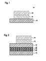
- Fig.1 shows a schematic fragmentary sectional view of a power module 1.
- the power module comprises a circuit arrangement according to a first embodiment of the invention consisting of a power semiconductor 20 and a punched grid 30, which constitutes the circuit carrier. Between the power semiconductor 20 and the punched grid / circuit carrier 30, the metal-ceramic composite material layer 10 is arranged so that it has in material-locking contact both to the power semiconductor 20 and the circuit substrate 30.
- both the thermo-mechanical differences resulting from the different materials of the power semiconductor 20 (semiconductor material such as silicon, etc.) and the circuit carrier 30 (which essentially consists of metal) largely compensate each other or none lead only insignificantly life-like efficiency losses of the power module 1.
- Fig. 2 a schematic partial sectional view of a power module according to a second embodiment of the invention.
- Components associated with the Power module off Fig. 1 are identical, are provided with the same reference numerals and will not be discussed again.
- the power module off Fig. 2 is different from that Fig. 1 in that a circuit carrier is formed, in which further MMC metal and ceramic layers are provided. Specifically, these are an intermediate layer 40 made of a metal-ceramic composite material layer, a ceramic layer 50, a further intermediate layer 60 made of a metal-ceramic composite material layer and a metal layer 70.
Landscapes
- Cooling Or The Like Of Semiconductors Or Solid State Devices (AREA)
- Die Bonding (AREA)
Applications Claiming Priority (1)
| Application Number | Priority Date | Filing Date | Title |
|---|---|---|---|
| DE102011083906A DE102011083906A1 (de) | 2011-09-30 | 2011-09-30 | Fügehilfe für ein Leistungsmodul |
Publications (2)
| Publication Number | Publication Date |
|---|---|
| EP2575169A2 true EP2575169A2 (fr) | 2013-04-03 |
| EP2575169A3 EP2575169A3 (fr) | 2016-11-09 |
Family
ID=47073283
Family Applications (1)
| Application Number | Title | Priority Date | Filing Date |
|---|---|---|---|
| EP12185297.4A Withdrawn EP2575169A3 (fr) | 2011-09-30 | 2012-09-20 | Dispositif d'aide à l'assemblage pour un module de puissance |
Country Status (2)
| Country | Link |
|---|---|
| EP (1) | EP2575169A3 (fr) |
| DE (1) | DE102011083906A1 (fr) |
Families Citing this family (1)
| Publication number | Priority date | Publication date | Assignee | Title |
|---|---|---|---|---|
| DE102015215571A1 (de) * | 2015-08-14 | 2017-02-16 | Siemens Aktiengesellschaft | Kühlkörper für eine elektronische Komponente und Verfahren zu dessen Herstellung |
Family Cites Families (7)
| Publication number | Priority date | Publication date | Assignee | Title |
|---|---|---|---|---|
| US3497774A (en) * | 1967-06-07 | 1970-02-24 | Beckman Instruments Inc | Electrical circuit module and method of manufacture |
| US4436785A (en) * | 1982-03-08 | 1984-03-13 | Johnson Matthey Inc. | Silver-filled glass |
| EP0477600A1 (fr) * | 1990-09-26 | 1992-04-01 | Siemens Aktiengesellschaft | Procédé pour attacher à un substrat un corps semi-conducteur comportant au moins un composant semi-conducteur |
| US5775403A (en) * | 1991-04-08 | 1998-07-07 | Aluminum Company Of America | Incorporating partially sintered preforms in metal matrix composites |
| US5525374A (en) * | 1992-09-17 | 1996-06-11 | Golden Technologies Company | Method for making ceramic-metal gradient composites |
| DE10260851B4 (de) * | 2002-12-23 | 2013-07-18 | Robert Bosch Gmbh | Verfahren zur Herstellung einer Kühlvorrichtung für Leistungsbauelemente, Kühlvorrichtung und elektronisches Steuergerät |
| DE102010001565A1 (de) * | 2010-02-04 | 2011-08-04 | Robert Bosch GmbH, 70469 | Leistungsmodul mit einer Schaltungsanordnung, elektrische/elektronische Schaltungsanordnung, Verfahren zur Herstellung eines Leistungsmoduls |
-
2011
- 2011-09-30 DE DE102011083906A patent/DE102011083906A1/de not_active Withdrawn
-
2012
- 2012-09-20 EP EP12185297.4A patent/EP2575169A3/fr not_active Withdrawn
Non-Patent Citations (1)
| Title |
|---|
| None |
Also Published As
| Publication number | Publication date |
|---|---|
| DE102011083906A1 (de) | 2013-04-04 |
| EP2575169A3 (fr) | 2016-11-09 |
Similar Documents
| Publication | Publication Date | Title |
|---|---|---|
| DE102010003533B4 (de) | Substratanordnung, Verfahren zur Herstellung einer Substratanordnung, Verfahren zur Herstellung eines Leistungshalbleitermoduls und Verfahren zur Herstellung einer Leistungshalbleitermodulanordnung | |
| EP3386934B1 (fr) | Substrat en cuivre-céramique, produit semi-fini en cuivre pour la fabrication d'un substrat en cuivre-céramique et procédé pour la fabrication d'un substrat en cuivre-céramique | |
| WO2010136017A1 (fr) | Unité modulaire électrique refroidie | |
| EP3858116B1 (fr) | Substrat de support pour composants électriques, en particulier électroniques, et procédé de fabrication d'un substrat de support | |
| DE102014221636A1 (de) | Halbleitermodul und Verfahren zum Herstellen desselben | |
| DE112018001239B4 (de) | Halbleiterbauelement, verfahren zur herstellung desselben und halbleitermodul | |
| DE102016104844A1 (de) | Verfahren zur Herstellung eines Chipverbunds | |
| DE102014119386B4 (de) | Verfahren zum Herstellen eines Metall-Keramik-Substrates und zugehöriges Metall-Keramik-Substrat | |
| WO2017140571A1 (fr) | Procédé de fabrication d'une plaque de dissipation thermique, plaque de dissipation thermique, procédé de fabrication d'un module à semi-conducteur et module à semi-conducteur | |
| EP3632190A1 (fr) | Sous-ensemble électrique et son procédé de fabrication | |
| DE102012211952A1 (de) | Leistungshalbleitermodul mit mindestens einem stressreduzierenden Anpasselement | |
| WO2012152364A1 (fr) | Substrat doté d'une zone électriquement neutre | |
| DE102014213490C5 (de) | Kühlvorrichtung, Verfahren zur Herstellung einer Kühlvorrichtung und Leistungsschaltung | |
| DE102011005206A1 (de) | Thermoelektrischer Generator | |
| DE112016007096T5 (de) | Halbleitervorrichtung | |
| DE102008055137A1 (de) | Elektrisches oder elektronisches Verbundbauteil sowie Verfahren zum Herstellen eines elektrischen oder elektronischen Verbundbauteils | |
| DE102009022877B4 (de) | Gekühlte elektrische Baueinheit | |
| DE102019135146A1 (de) | Metall-Keramik-Substrat und Verfahren zur Herstellung eines solchen Metall-Keramik-Substrats | |
| EP2575169A2 (fr) | Dispositif d'aide à l'assemblage pour un module de puissance | |
| DE202015006897U1 (de) | Halbleitermodul und Leistungsanordnung | |
| EP3384527B1 (fr) | Module électronique de puissance | |
| WO2022171857A1 (fr) | Élément chauffant à coefficient de température positif (ctp), dispositif de chauffage électrique et utilisation d'un élément chauffant ctp | |
| EP2327095B1 (fr) | Ensemble semi-conducteur et procédé de fabrication d'un ensemble semi-conducteur | |
| DE10249855B4 (de) | Werkstoff zum Zuführen von Strom auf Halbleiter-Bauelemente und Verfahren zum Herstellen eines solchen | |
| AT510473B1 (de) | Thermogenerator |
Legal Events
| Date | Code | Title | Description |
|---|---|---|---|
| PUAI | Public reference made under article 153(3) epc to a published international application that has entered the european phase |
Free format text: ORIGINAL CODE: 0009012 |
|
| AK | Designated contracting states |
Kind code of ref document: A2 Designated state(s): AL AT BE BG CH CY CZ DE DK EE ES FI FR GB GR HR HU IE IS IT LI LT LU LV MC MK MT NL NO PL PT RO RS SE SI SK SM TR |
|
| AX | Request for extension of the european patent |
Extension state: BA ME |
|
| RIC1 | Information provided on ipc code assigned before grant |
Ipc: H01L 23/48 20060101ALI20160718BHEP Ipc: H01L 23/492 20060101ALI20160718BHEP Ipc: H01L 23/495 20060101AFI20160718BHEP Ipc: H01L 23/00 20060101ALI20160718BHEP |
|
| PUAL | Search report despatched |
Free format text: ORIGINAL CODE: 0009013 |
|
| AK | Designated contracting states |
Kind code of ref document: A3 Designated state(s): AL AT BE BG CH CY CZ DE DK EE ES FI FR GB GR HR HU IE IS IT LI LT LU LV MC MK MT NL NO PL PT RO RS SE SI SK SM TR |
|
| AX | Request for extension of the european patent |
Extension state: BA ME |
|
| RIC1 | Information provided on ipc code assigned before grant |
Ipc: H01L 23/495 20060101AFI20161004BHEP Ipc: H01L 23/492 20060101ALI20161004BHEP Ipc: H01L 23/48 20060101ALI20161004BHEP Ipc: H01L 23/00 20060101ALI20161004BHEP |
|
| 17P | Request for examination filed |
Effective date: 20170509 |
|
| RBV | Designated contracting states (corrected) |
Designated state(s): AL AT BE BG CH CY CZ DE DK EE ES FI FR GB GR HR HU IE IS IT LI LT LU LV MC MK MT NL NO PL PT RO RS SE SI SK SM TR |
|
| STAA | Information on the status of an ep patent application or granted ep patent |
Free format text: STATUS: THE APPLICATION IS DEEMED TO BE WITHDRAWN |
|
| 18D | Application deemed to be withdrawn |
Effective date: 20170510 |