EP2575168A1 - Elektronische Vorrichtung - Google Patents
Elektronische Vorrichtung Download PDFInfo
- Publication number
- EP2575168A1 EP2575168A1 EP12181981A EP12181981A EP2575168A1 EP 2575168 A1 EP2575168 A1 EP 2575168A1 EP 12181981 A EP12181981 A EP 12181981A EP 12181981 A EP12181981 A EP 12181981A EP 2575168 A1 EP2575168 A1 EP 2575168A1
- Authority
- EP
- European Patent Office
- Prior art keywords
- semiconductor package
- main board
- plate
- electronic device
- bolster plate
- Prior art date
- Legal status (The legal status is an assumption and is not a legal conclusion. Google has not performed a legal analysis and makes no representation as to the accuracy of the status listed.)
- Withdrawn
Links
Images















Classifications
-
- H—ELECTRICITY
- H10—SEMICONDUCTOR DEVICES; ELECTRIC SOLID-STATE DEVICES NOT OTHERWISE PROVIDED FOR
- H10W—GENERIC PACKAGES, INTERCONNECTIONS, CONNECTORS OR OTHER CONSTRUCTIONAL DETAILS OF DEVICES COVERED BY CLASS H10
- H10W40/00—Arrangements for thermal protection or thermal control
- H10W40/60—Securing means for detachable heating or cooling arrangements, e.g. clamps
- H10W40/611—Bolts or screws
-
- H—ELECTRICITY
- H10—SEMICONDUCTOR DEVICES; ELECTRIC SOLID-STATE DEVICES NOT OTHERWISE PROVIDED FOR
- H10W—GENERIC PACKAGES, INTERCONNECTIONS, CONNECTORS OR OTHER CONSTRUCTIONAL DETAILS OF DEVICES COVERED BY CLASS H10
- H10W40/00—Arrangements for thermal protection or thermal control
- H10W40/20—Arrangements for cooling
- H10W40/231—Arrangements for cooling characterised by their places of attachment or cooling paths
-
- H—ELECTRICITY
- H10—SEMICONDUCTOR DEVICES; ELECTRIC SOLID-STATE DEVICES NOT OTHERWISE PROVIDED FOR
- H10W—GENERIC PACKAGES, INTERCONNECTIONS, CONNECTORS OR OTHER CONSTRUCTIONAL DETAILS OF DEVICES COVERED BY CLASS H10
- H10W40/00—Arrangements for thermal protection or thermal control
- H10W40/20—Arrangements for cooling
- H10W40/231—Arrangements for cooling characterised by their places of attachment or cooling paths
- H10W40/237—Arrangements for cooling characterised by their places of attachment or cooling paths attached to additional arrangements for cooling
-
- H—ELECTRICITY
- H10—SEMICONDUCTOR DEVICES; ELECTRIC SOLID-STATE DEVICES NOT OTHERWISE PROVIDED FOR
- H10W—GENERIC PACKAGES, INTERCONNECTIONS, CONNECTORS OR OTHER CONSTRUCTIONAL DETAILS OF DEVICES COVERED BY CLASS H10
- H10W40/00—Arrangements for thermal protection or thermal control
- H10W40/20—Arrangements for cooling
- H10W40/231—Arrangements for cooling characterised by their places of attachment or cooling paths
- H10W40/242—Arrangements for cooling characterised by their places of attachment or cooling paths comprising thermal conductors between chips and the and the arrangements for cooling, e.g. compliant heat-spreaders
-
- H—ELECTRICITY
- H10—SEMICONDUCTOR DEVICES; ELECTRIC SOLID-STATE DEVICES NOT OTHERWISE PROVIDED FOR
- H10W—GENERIC PACKAGES, INTERCONNECTIONS, CONNECTORS OR OTHER CONSTRUCTIONAL DETAILS OF DEVICES COVERED BY CLASS H10
- H10W40/00—Arrangements for thermal protection or thermal control
- H10W40/60—Securing means for detachable heating or cooling arrangements, e.g. clamps
-
- H—ELECTRICITY
- H10—SEMICONDUCTOR DEVICES; ELECTRIC SOLID-STATE DEVICES NOT OTHERWISE PROVIDED FOR
- H10W—GENERIC PACKAGES, INTERCONNECTIONS, CONNECTORS OR OTHER CONSTRUCTIONAL DETAILS OF DEVICES COVERED BY CLASS H10
- H10W40/00—Arrangements for thermal protection or thermal control
- H10W40/60—Securing means for detachable heating or cooling arrangements, e.g. clamps
- H10W40/625—Clamping parts not primarily conducting heat
-
- H—ELECTRICITY
- H10—SEMICONDUCTOR DEVICES; ELECTRIC SOLID-STATE DEVICES NOT OTHERWISE PROVIDED FOR
- H10W—GENERIC PACKAGES, INTERCONNECTIONS, CONNECTORS OR OTHER CONSTRUCTIONAL DETAILS OF DEVICES COVERED BY CLASS H10
- H10W72/00—Interconnections or connectors in packages
- H10W72/851—Dispositions of multiple connectors or interconnections
- H10W72/874—On different surfaces
- H10W72/877—Bump connectors and die-attach connectors
-
- H—ELECTRICITY
- H10—SEMICONDUCTOR DEVICES; ELECTRIC SOLID-STATE DEVICES NOT OTHERWISE PROVIDED FOR
- H10W—GENERIC PACKAGES, INTERCONNECTIONS, CONNECTORS OR OTHER CONSTRUCTIONAL DETAILS OF DEVICES COVERED BY CLASS H10
- H10W90/00—Package configurations
- H10W90/701—Package configurations characterised by the relative positions of pads or connectors relative to package parts
- H10W90/721—Package configurations characterised by the relative positions of pads or connectors relative to package parts of bump connectors
- H10W90/724—Package configurations characterised by the relative positions of pads or connectors relative to package parts of bump connectors between a chip and a stacked insulating package substrate, interposer or RDL
Definitions
- the embodiments discussed herein are related to an electronic device that includes a heat-dissipating structure.
- a methodology of mounting a large-size semiconductor package on a main board include a Ball Grid Array (BGA) mounting methodology, a Pin Grid Array (PGA) mounting methodology, and a Land Grid Array (LGA) mounting methodology.
- BGA Ball Grid Array
- PGA Pin Grid Array
- LGA Land Grid Array
- FIG. 1A is a diagram of an example of a connection structure between a semiconductor package 100 and a main board 101 that uses the BGA mounting methodology.
- BGA mounting methodology solder balls 102 are placed on a lower surface (a back surface) of the semiconductor package 100, and the semiconductor package 100 and the main board 101 are coupled via the solder balls 102.
- FIG. 1B is a diagram of an example of a connection structure between the semiconductor package 100 and the main board 101 that uses the PGA mounting methodology.
- the semiconductor package 100 and the main board 101 are coupled via pins 103 provided on the lower surface of the semiconductor package 100.
- FIG. 1C is a diagram of an example of a connection structure between the semiconductor package 100 and the main board 101 that uses the LGA mounting methodology.
- an LGA socket 104 is placed between the semiconductor package 100 and the main board 101, and the semiconductor package 100 and the main board 101 are coupled via the LGA socket 104.
- a mounting methodology is selected based on the usage purpose in light of factors such as reliability, exchange frequency, and cost of a connecting unit between the semiconductor package and the main board.
- a load pressure
- the semiconductor package mounted on the main board By applying a load (pressure) to the semiconductor package to mount the semiconductor package on the main board, an electrical connection between the semiconductor package and the main board is obtained.
- the amount of heat of a semiconductor chip increases in response to high-speed operation of the semiconductor chip, and therefore the semiconductor package is desired to be cooled down.
- a cooling structure that is a heat dissipation device such as a heat sink or a cooling unit, is mounted on the semiconductor package.
- the cooling structure that is a heat dissipation device mounted on the semiconductor package by applying a load to the heat dissipation device, the contact area with the semiconductor package is increased, thereby decreasing heat resistance.
- a load is applied to mount the semiconductor package on the main board or to mount the heat dissipation device on the semiconductor package.
- various ways of load application have been suggested.
- the heat dissipation device is mounted on the semiconductor package.
- a load when mounting the semiconductor package on the main board and a load with respect to the heat dissipation device are applied by the same loading device, thereby simplifying the structure
- the load to mount the semiconductor package on the main board is increasing.
- the semiconductor package is interposed between the heat dissipation device and the main board, and the load is applied to the heat dissipation device and the main board in an area outside of the semiconductor package, the load applied to the center portion of the main board is light, and the load applied to a portion outside of the center portion of the main board is heavy.
- warping may occur in the main board, the space between the semiconductor package and the main board may become nonuniform, and the electrical connection between the semiconductor package and the main board may become insufficient. It is desirable to suppress unevenness of a space between an electronic device and a wiring board when the electronic device is mounted on the wiring board.
- unevenness of a space between the electronic device and the wiring board may be suppressed when the electronic device is mounted on the wiring board.
- an electronic device includes: a first plate; a wiring board arranged on the first plate and configured to have a plurality of first terminals on a surface opposite to a surface facing the first plate; an electronic component arranged above the wiring board and configured to have a plurality of second terminals on a surface facing the wiring board; a connecting unit arranged between the wiring board and the electronic component and configured to electrically couple the first terminals and the second terminals; a second plate arranged on the electronic component; a fixing unit arranged in an area outside of an area where the electronic component is placed and configured to pressurize the first plate and the second plate so that narrow a space between the first plate and the second plate; and a pressing unit arranged below the area where the electronic component is placed and configured to press the wiring board toward the electronic component.
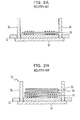
- FIG. 2A to FIG. 2E are diagrams each depicting a process of mounting a semiconductor package 53 on a main board 52 with an LGA mounting methodology in an electronic device 51 according to a comparative example.
- a bolster plate 54 is placed below a main board 52, and an LGA socket 55 is placed on the main board 52.
- the bolster plate 54 is provided with support shafts 56.
- the support shafts 56 each pass through a through hole provided in the main board 52 and protrude from the through hole provided in the main board 52.
- the semiconductor package 53 is placed on the LGA socket 55.
- Terminal electrodes of the semiconductor package 53 and pins (leads) of the LGA socket 55 are in contact with each other, and terminal electrodes of the main board 52 and pins (leads) of the LGA socket 55 are in contact with each other.
- the terminal electrodes of the semiconductor package 53 and the terminal electrodes of the main board 52 are electrically coupled to each other via the LGA socket 55.
- a heat sink 57 is placed above the semiconductor package 53.
- the heat sink 57 has a base plate 58 and fins 59.
- the support shafts 56 each pass through a through hole provided in the base plate 58, and a tip of each support shaft 56 protrudes from the base plate 58.
- a spring 60 and a nut 61 are placed on the tip of each support shaft 56.
- the spring 60 is compressed.
- a load (a pressure) is applied from the spring 60 to the base plate 58 in a direction in which the base plate 58 gets close to the bolster plate 54.
- the support shaft 56 is pulled up, and thus a load (a pressure) is applied from the support shaft 56 to the bolster plate 54 in a direction in which the bolster plate 54 gets close to the base plate 58. Therefore, with the support shaft 56, the spring 60, and the nut 61, a load (a pressure) is applied to the bolster plate 54 and the base plate 58 so that a space between the bolster plate 54 and the base plate 58 is narrowed.
- the support shafts 56 penetrate through the main board 52 and the base plate 58, the support shafts 56 are placed in an area outside of an area where the semiconductor package 53 is placed. Therefore, a load is applied to the bolster plate 54 and the base plate 58 in the area outside of the area where the semiconductor package 53 is placed. For this reason, the load applied to the center portion of the bolster plate 54 is relatively light, and the load applied to the portion outside the center portion of the bolster plate 54 is relatively heavy.
- the load applied to the center portion of the base plate 58 is relatively light, and the load applied to the portion outside the center portion of the base plate 58 is relatively heavy. As depicted in FIG.
- the main board 52 placed above the bolster plate 54 also warps in a concave shape. For this reason, the space between the main board 52 and the LGA socket 55 becomes uneven. For example, the space between the main board 52 and the LGA socket 55 becomes large at a center portion of the LGA socket 55, and the space between the main board 52 and the LGA socket 55 becomes small at ends of the LGA socket 55. Therefore, a large difference occurs between a maximum value of the space between the main board 52 and the LGA socket 55 and a minimum value of the space between the main board 52 and the LGA socket 55.
- the contact between the terminal of the main board 52 and the pins of the LGA socket 55 becomes uneven, causing electrical contact between the main board 52 and the semiconductor package 53 via the LGA socket 55 to become insufficient and degrading reliability of the electronic device.
- the terminal of the main board 52 and the pins of the LGA socket 55 may not be in contact with each other, or the pins of the LGA socket 55 may be bent.
- the semiconductor package 53 below the base plate 58 also warps in a convex shape. For this reason, the space between the semiconductor package 53 and the LGA socket 55 becomes uneven. For example, the space between the semiconductor package 53 and the LGA socket 55 becomes large at the center portion of the LGA socket 55, and the space between the semiconductor package 53 and the LGA socket 55 becomes small at the ends of the LGA socket 55. Therefore, a large difference occurs between a maximum value of the space between the semiconductor package 53 and the LGA socket 55 and a minimum value of the space between the semiconductor package 53 and the LGA socket 55.
- the contact between the terminal of the semiconductor package 53 and the pins of the LGA socket 55 becomes uneven, causing electrical contact between the main board 52 and the semiconductor package 53 via the LGA socket 55 to become insufficient and degrading reliability of the electronic device.
- the terminal of the semiconductor package 53 and the pins of the LGA socket 55 may not be in contact with each other, or the pins of the LGA socket 55 may be bent.
- FIG. 3 is an image view of the space between the main board 52 and the semiconductor package 53 in the electronic device 51 according to the comparative example. As depicted in FIG. 3 , the space is large between the center portion of the main board 52 and the center portion of the semiconductor package 53, and the space is small between the ends of the main board 52 and the ends of the semiconductor package 53. Arrows in FIG. 3 represent loads applied to the main board 52 and the semiconductor package 53. The length of each arrow in FIG. 3 represents the magnitude of a load applied to the main board 52 or the semiconductor package 53.
- the size of the base plate 58 in a plane direction is larger than the size of the semiconductor package 53 in a plane direction. For this reason, the magnitude of warping of the base plate 58 is larger than the magnitude of warping of the semiconductor package 53, causing a space between the semiconductor package 53 and the base plate 58.
- the center portion of the semiconductor package 53 and the center portion of the base plate 58 are not in contact with each other. As a result, heat transmission from the semiconductor package 53 to the heat sink 57 is decreased, and the heat dissipation capability of the semiconductor package 53 is degraded.
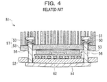
- FIG. 4 is a cross-sectional view of the electronic device 51 according to the comparative example, depicting a case in which the semiconductor package 53 is mounted on the main board 52 with the BGA mounting methodology.
- the space between the main board 52 and the semiconductor package 53 is uneven.
- a space between the main board 52 and an outer peripheral portion of the semiconductor package 53 is narrow, and solder balls 62 placed on a lower surface (a back surface) of the semiconductor package 53 are deformed.
- large loads are applied to corner portions of the semiconductor package 53, compressive stress concentrates on the solder balls 62 placed at the corner portions of the lower surface of the semiconductor package 53, and the solder balls 62 are gradually crushed. For this reason, due to creep deformation of the solder balls 62 placed at the corner portions of the lower surface of the semiconductor package 53, the electrical connection between the main board 52 and the semiconductor package 53 becomes insufficient, thereby degrading reliability of the electronic device.
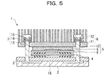
- FIG. 5 is a cross-sectional view of an electronic device 1 according to a first embodiment.
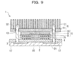
- the electronic device 1 according to the first embodiment has a bolster plate 2, a main board 3, an LGA socket 4, a semiconductor package 5, a heat sink 6, and fixing units 7.
- the bolster plate 2 is an example of a first plate.
- the main board 3 is an example of a wiring board.
- the LGA socket 4 is an example of a connecting unit.
- the semiconductor package 5 is an example of an electronic component.
- the main board 3 is placed above the bolster plate 2.
- the LGA socket 4 is placed on the main board 3.
- the semiconductor package 5 is placed on the LGA socket 4.
- the heat sink 6 is placed on the semiconductor package 5.
- the semiconductor package 5 has a package substrate 8, a semiconductor chip (a semiconductor element) 9, and a heat spreader 10.
- the heat sink 6 has a base plate 11 and fins 12.
- the base plate 11 is an example of a second plate.
- Each of the fixing units 7 has a support shaft 13, a spring 14, and a nut 15.
- the fixing unit 7 is placed in an area outside of an area where the semiconductor package 5 is placed.
- a projection 16 is provided on an upper surface of the bolster plate 2.
- the projection 16 is an example of a pressing unit.
- the upper surface of the bolster plate 2 is a surface where the main board 3 is placed.
- the projection 16 presses the main board 3 in a direction of the area where the semiconductor package 5 is placed.
- the projection 16 is provided below the area where the semiconductor package 5 is placed.
- FIG. 6A is a cross-sectional view of the bolster plate 2 that is provided with the support shafts 13.
- stainless steel may be used as the material of the bolster plate 2 and the support shafts 13.
- the support shaft 13 With each support shaft 13 inserted in a shaft hole provided in the bolster plate 2, the support shaft 13 may be fixed to the bolster plate 2.
- a through hole penetrating through the bolster plate 2 may be provided in the bolster plate 2, and the support shaft 13 may be inserted through the through hole and fixed with a fixture from a lower surface (a back surface) of the bolster plate 2.
- the lower surface of the bolster plate 2 is the surface opposite to the surface that faces the main board 3.
- FIG. 6B is a top view of the bolster plate 2 provided with the support shafts 13.
- the projection 16 is provided at the center portion of the bolster plate 2
- a support 17 is provided in an outer peripheral portion of the bolster plate 2. Therefore, a step is formed between the center portion and the outer peripheral portion of the bolster plate 2.
- stainless steel may be used as the material of the projection 16 and the support 17.
- the projection 16 and the support 17 may have a cubic shape or a columnar shape.
- the projection 16 and the support 17 have the same height.
- a portion of the upper surface of the bolster plate 2 positioned between the projection 16 and the support 17 is referred to as the base surface of the bolster plate 2.
- the support shafts 13 are provided on the base surface of the bolster plate 2.
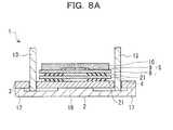
- the main board 3 is placed on the bolster plate 2.
- a resin substrate may be used as a material of the main board 3.
- the support shafts 13 each pass through a through hole 20 provided in the main board 3 and protrude from the through hole 20 provided in the main board 3.
- the support shafts 13 may be fixed to the bolster plate 2 by placing the main board 3 on the bolster plate 2, inserting the support shafts 13 in the through holes 20 provided in the main board 3, and then inserting the support shafts 13 in shaft holes provided in the bolster plate 2.
- the LGA socket 4 is placed on the main board 3, and the semiconductor package 5 is placed on the LGA socket 4.
- a plurality of terminal electrodes are provided on an upper surface of the main board 3.
- the upper surface of the main board 3 is a surface where the semiconductor package 5 is placed and is the surface opposite to the surface facing the bolster plate 2.
- the LGA socket 4 has pins (leads) 21 as connection terminals.
- the pins 21 of the LGA socket 4 penetrate through the LGA socket 4 and protrude from the upper and lower surfaces of the LGA socket 4.
- a semiconductor chip 9 is provided on the package substrate 8.
- the semiconductor chip 9 is electrically coupled to (mounted on) the package substrate 8 with, for example, a flip chip connection.
- the heat spreader 10 is provided on the package substrate 8 so as to cover the upper surface and side surfaces of the semiconductor chip 9.
- a metal such as copper may be used as a material of the heat spreader 10.
- the lower surface of the semiconductor package 5 is the surface facing the main board 3 and the surface opposite to a surface where the heat sink 6 is placed.
- FIG. 8B is a top view of the electronic device 1 according to the first embodiment when the LGA socket 4 is placed on the main board 3 and the semiconductor package 5 is placed on the LGA socket 4. Here, the position where the projection 16 is placed is described.
- the area where the LGA socket 4 is placed is divided by the number of support shafts 13 to be placed.
- the number of support shafts 13 to be placed is four, the area where the LGA socket 4 is placed is divided into four.
- the projection 16 is provided on the bolster plate 2 so that the outer peripheral portion of the projection 16 passes center of gravity points (G1 to G4 in FIG. 8B ) of the respective divided areas.
- the projection 16 has a cubic shape, the projection 16 is provided on the bolster plate 2 so that four corners of the upper surface of the projection 16 pass the center of gravity points of the respective divided areas.
- the position where the projection 16 is placed described above is merely an example, and the projection 16 may be provided at a position other than the above.
- the heat sink 6 is placed on the semiconductor package 5.
- aluminum, copper, aluminum nitride, or the like may be used as the material of the base plate 11 and the fins 12. Heat occurring at the semiconductor chip 9 is transmitted via the heat spreader 10 to the heat sink 6 and is dissipated by the heat sink 6.
- the support shafts 13 each pass the through hole 22 provided in the base plate 11, and the tip of each support shaft 13 protrudes from the base plate 11.
- a thermally conductive material such as aluminum, copper, or aluminum nitride may be interposed between the semiconductor package 5 and the base plate 11.
- a spring 14 and a nut 15 are placed on the tip of each support shaft 13.
- the spring 14 is compressed by fastening the nut 15.
- a load (a pressure) is applied from the spring 14 to the base plate 11 in a direction in which the base plate 11 gets close to the bolster plate 2.
- the support shaft 13 is pulled up, and thus a load (a pressure) is applied from the support shaft 13 to the bolster plate 2 in a direction in which the bolster plate 2 gets close to the base plate 11. Therefore, with the support shaft 13, the spring 14, and the nut 15, a load (a pressure) is applied to the bolster plate 2 and the base plate 11 so that a space between the bolster plate 2 and the base plate 11 may be narrowed.
- the support shafts 13 penetrate through the main board 3 and the base plate 11, the support shafts 13 are provided at the outer peripheral portion of the bolster plate 2. That is, the support shafts 13 are placed in an area outside an area where the semiconductor package 5 is placed. Therefore, a load is applied to the base plate 11 in the area outside the area where the semiconductor package 5 is placed. For this reason, the load applied to a center portion of the base plate 11 is light, and the load applied to a portion outside the center portion of the base plate 11 is heavier. When the load is applied to the base plate 11 in the area outside of the area where the semiconductor package 5 is placed, the base plate 11 warps in a convex shape.
- the projection 16 and the support 17 are in contact with the lower surface (the back surface) of the main board 3, and the base surface of the bolster plate 2 is not in contact with the lower surface of the main board 3.
- the lower surface of the main board 3 is the surface facing the bolster plate 2 and is the surface opposite to the surface where the semiconductor package 5 is placed.
- a space is formed between the bolster plate 2 and the main board 3 so as to surround each support shaft 13.
- a space is formed between the bolster plate 2 and the main board 3 with the space surrounding the projection 16.
- a dotted line B in FIG. 12 represents a deformed image of the main board 3.
- the LGA socket 4 and the semiconductor package 5 are placed at the center portion of the upper surface of the main board 3. For this reason, with the center portion of the main board 3 warping in a convex shape, the LGA socket 4 and the semiconductor package 5 warp in a convex shape. With the center portion of the main board 3 warping in a convex shape and the LGA socket 4 also warping in a convex shape, unevenness of the space between the main board 3 and the LGA socket 4 may be suppressed. In addition, with the LGA socket 4 warping in a convex shape and the semiconductor package 5 also warping in a convex shape, unevenness of the space between the LGA socket 4 and the semiconductor package 5 may be suppressed.
- the terminal electrodes of the main board 3 and the pins 21 of the LGA socket 4 are uniformly in contact with each other, and the pins 21 of the LGA socket 4 and the terminal electrodes of the semiconductor package 5 are uniformly in contact with each other, thereby maintaining an electrical connection between the main board 3 and the semiconductor package 5 via the LGA socket 4.
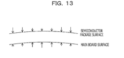
- FIG. 13 is an image view of the space between the main board 3 and the semiconductor package 5 in the electronic device 1 according to the first embodiment. As depicted in FIG. 13 , unevenness of the space between the main board 3 and the semiconductor package 5 is suppressed. Arrows in FIG. 13 represent loads applied to the main board 3 and the semiconductor package 5. The length of each arrow in FIG. 13 represents the magnitude of the load applied to the main board 3 or the semiconductor package 5.
- the electronic device 1 according to the first embodiment since the load is applied from the projection 16 to the center portion of the lower surface of the main board 3, warping of the semiconductor package 5 is larger, compared with the electronic device 51 according to the comparative example. Therefore, according to the electronic device 1 of the first embodiment, unevenness of the space between the semiconductor package 5 and the base plate 11 may be suppressed. That is, according to the electronic device 1 of the first embodiment, the ratio of contact between the semiconductor package 5 and the base plate 11 is increased. As a result, heat transmission from the semiconductor package 5 to the heat sink 6 may be improved, and heat dissipation capability of the semiconductor package 5 may be improved.
- the ratio of contact between the semiconductor package 5 and the thermally conductive material and the ratio of contact between the base plate 11 and the thermally conductive material may be increased.
- heat transmission from the semiconductor package 5 to the heat sink 6 may be improved, and heat dissipation capability of the semiconductor package 5 may be improved.
- the projection 16 and the support 17 are provided as part of the bolster plate 2, and a load is applied from the projection 16 and the support 17 to the main board 3, thereby mounting the semiconductor package 5 on the main board 3.
- a load applied from the projection 16 to the main board 3 an electrical connection between the semiconductor package 5 and the main board 3 may be insufficient.
- the projection 16 and the support 17 are provided as part of the bolster plate 2, and a load is applied from the projection 16 and the support 17 to the main board 3.
- a stable electrical connection between the main board 3 and the semiconductor package 5 may be obtained.
- a stable electrical connection between the main board 3 and the semiconductor package 5 may be obtained by applying a load from the projection 16 to the main board 3, not providing the support 17 as part of the bolster plate 2 may be an option.
- a cover plate (a plate member) 23 may be provided between the bolster plate 2 and the main board 3 as depicted in FIG. 14 . That is, the cover plate 23 may be placed on the projection 16 and the support 17.
- the cover plate 23 may be laminated to the lower surface of the bolster plate 2 with an adhesive.
- a material with a stiffness higher than that of the main board 3 is preferably used.
- stainless steel may be used. Because the main board 3 tends to be made thinner, the stiffness of the main board 3 declines. When the main board 3 has a low stiffness, by applying a load from the projection 16 and the support 17 to the main board 3, the main board 3 may be bent.
- FIG. 15 is a cross-sectional view of the electronic device 1 according to a second embodiment. Note that elements identical to those in the first embodiment are each provided with the same reference numeral as that of the first embodiment and are not described herein.
- a plurality of projections 24 are provided on the upper surface of the bolster plate 2.
- the projections 24 are an example of the pressing unit. As a material of the projections 24, stainless steel may be used.
- Each of the projections 24 may be in a cubic shape or a columnar shape.
- the projections 24 and the support 17 have the same height.
- the plurality of projections 24 press the main board 3 toward the semiconductor package 5. That is, the plurality of projections 24 press the main board 3 in the direction of the area where the semiconductor package 5 is placed.
- the plurality of projections 24 are provided below the area where the semiconductor package 5 is placed. For this reason, with the plurality of projections 24 pressing the main board 3 toward the semiconductor package 5, unevenness of the space between the main board 3 and the semiconductor package 5 may be suppressed.
- the terminal electrodes of the main board 3 and the pins 21 of the LGA socket 4 may be uniformly in contact with each other.
- the pins 21 of the LGA socket 4 and the terminal electrodes of the semiconductor package 5 being uniformly in contact with each other, an electrical connection between the main board 3 and the semiconductor package 5 via the LGA socket 4 may be maintained.
- the electronic device 1 according to the second embodiment since the load is applied from the plurality of projections 24 to the center portion of the lower surface of the main board 3, warping of the semiconductor package 5 is larger, compared with the electronic device 51 according to the comparative example. Therefore, according to the electronic device 1 of the second embodiment, unevenness of the space between the semiconductor package 5 and the base plate 11 may be suppressed. That is, according to the electronic device 1 of the second embodiment, the ratio of contact between the semiconductor package 5 and the base plate 11 may be increased. As a result, heat transmission from the semiconductor package 5 to the heat sink 6 may be improved, and heat dissipation capability of the semiconductor package 5 may be improved.
- the ratio of contact between the semiconductor package 5 and the thermally conductive material and the ratio of contact between the base plate 11 and the thermally conductive material may be increased.
- heat transmission from the semiconductor package 5 to the heat sink 6 is improved, and heat dissipation capability of the semiconductor package 5 may be improved.
- the support 17 and the plurality of projections 24 are provided as part of the bolster plate 2, and a load is applied from the support 17 and the plurality of projections 24 to the main board 3, thereby mounting the semiconductor package 5 on the main board 3.
- a load is applied from the plurality of projections 24 to the main board 3.
- the support 17 and the plurality of projections 24 are provided as part of the bolster plate 2, and a load is applied from the support 17 and the plurality of projections 24 to the main board 3.
- a stable electrical connection between the main board 3 and the semiconductor package 5 may be obtained.
- a stable electrical connection between the main board 3 and the semiconductor package 5 may be obtained by applying a load from the plurality of projections 24 to the main board 3, not providing the support 17 as part of the bolster plate 2 is an option.
- FIG. 16 is a top view of the electronic device 1 according to the second embodiment when the LGA socket 4 is placed on the main board 3 and the semiconductor package 5 is placed on the LGA socket 4.
- the area where the LGA socket 4 is placed is divided by the number of support shafts 13 to be placed.
- the number of support shafts 13 to be placed is four, the area where the LGA socket 4 is placed is divided into four.
- the plurality of projections 24 are provided on the bolster plate 2 so that the plurality of projections 24 superpose center of gravity points (G1 to G4 in FIG. 16 ) of the respective divided areas.
- the positions where the plurality of projections 24 are placed described above are merely an example, and the projections 24 may be provided at positions other than the above.
- the number of projections 24 to be placed is not restricted to four, and may be a different number.
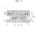
- the cover plate (the plate member) 23 may be provided between the bolster plate 2 and the main board 3 as depicted in FIG. 17 . That is, the cover plate 23 may be placed on the support 17 and the plurality of projections 24.
- the main board 3 has a low stiffness, by applying a load from the support 17 and the plurality of projections 24 to the main board 3, the main board 3 may be bent.
- partial concentration of the load applied from the support 17 and the plurality of projections 24 to the main board 3 may be suppressed, and bending of the main board 3 may be suppressed.
- FIG. 18 is a cross-sectional view of the electronic device 1 according to a third embodiment. Elements identical to those in the first embodiment are each provided with the same reference numeral as that of the first embodiment and are not described herein.
- a plurality of disc springs 30 are provided on the upper surface of the bolster plate 2.
- the disc springs 30 are an example of the pressing unit.
- the disc springs 30 are elastic bodies capable of obtaining a large restoring force with a small compression amount.
- the lower surface of the main board 3 and an upper surface of each disc spring 30 are in contact with each other.
- the plurality of disc springs 30 press the main board 3 toward the semiconductor package 5. That is, the plurality of disc springs 30 press the main board 3 in the direction of the area where the semiconductor package 5 is placed.
- the plurality of disc springs 30 are provided below the area where the semiconductor package 5 is placed. Thereby, with the plurality of disc springs 30 pressing the main board 3 toward the semiconductor package 5, unevenness of the space between the main board 3 and the semiconductor package 5 may be suppressed.
- the terminal electrodes of the main board 3 and the pins 21 of the LGA socket 4 may be uniformly in contact with each other, and the pins 21 of the LGA socket 4 and the terminal electrodes of the semiconductor package 5 may be uniformly in contact with each other, thereby maintaining an electrical connection between the main board 3 and the semiconductor package 5 via the LGA socket 4.
- the electronic device 1 according to the third embodiment since the load is applied from the plurality of disc springs 30 to the center portion of the lower surface of the main board 3, warping of the semiconductor package 5 is larger, compared with the electronic device 51 according to the comparative example. Therefore, according to the electronic device 1 of the third embodiment, unevenness of the space between the semiconductor package 5 and the base plate 11 may be suppressed. That is, according to the electronic device 1 of the third embodiment, the ratio of contact between the semiconductor package 5 and the base plate 11 may be increased. As a result, heat transmission from the semiconductor package 5 to the heat sink 6 may be improved, and heat dissipation capability of the semiconductor package 5 may be improved.
- the ratio of contact between the semiconductor package 5 and the thermally conductive material and the ratio of contact between the base plate 11 and the thermally conductive material may be increased.
- heat transmission from the semiconductor package 5 to the heat sink 6 may be improved, and heat dissipation capability of the semiconductor package 5 may be improved.
- the plurality of disc springs 30 are provided on the bolster plate 2 to cause the lower surface of the main board 3 and the upper surface of each of the disc springs 30 to be in contact with each other.
- the semiconductor package 5 is mounted on the main board 3.
- the main board 3 With the restoring force of the disc springs 30, the main board 3 may be efficiently pressed toward the semiconductor package 5. Therefore, with the plurality of disc springs 30 being provided on the bolster plate 2 and a load being applied from the plurality of disc springs 30 to the main board 3, a stable electrical connection between the main board 3 and the semiconductor package 5 may be obtained.
- the main board 3 may be efficiently pressed toward the semiconductor package 5. Therefore, the support 17 may be omitted from the outer peripheral portion of the upper surface of the bolster plate 2.
- a body with elasticity such as a coil spring or a rubber spring may be provided on the upper surface of the bolster plate 2 in place of the disc springs 30.
- the disc springs 30 may be provided at the same positions where the projections 24 are placed, which have been described in the second embodiment. Alternatively, the disc springs 30 may be provided at positions different from the positions where the projections 24 are placed, which were described in the second embodiment.
- the positions and number of the disc springs 30 to be placed may be determined depending on the size of the semiconductor package 5. For example, when the size of the semiconductor package 5 is small, one disc spring 30 may be provided on the center portion of the upper surface of the bolster plate 2.
- the cover plate (the plate member) 23 may be provided between the bolster plate 2 and the main board 3 as depicted in FIG. 19 . That is, the cover plate 23 may be placed above the plurality of disc springs 30.
- the main board 3 has a low stiffness, by applying a load from the plurality of disc springs 30 to the main board 3, the main board 3 may be bent.
- partial concentration of the load applied from the plurality of disc springs 30 to the main board 3 is suppressed, and bending of the main board 3 may be suppressed.
- the cover plate 23 when the support 17 is provided to the outer peripheral portion of the upper surface of the bolster plate 2, the cover plate 23 may be placed on the support 17 as depicted in FIG. 20 .
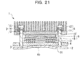
- FIG. 21 is a cross-sectional view of the electronic device 1 according to a fourth embodiment. Elements identical to those in the first embodiment are each provided with the same reference numeral as that of the first embodiment and are not described herein.
- the bolster plate 2 is produced in a plate spring shape. That is, a plate spring part 40 is integrally formed as part of the bolster plate 2.
- the plate spring part 40 is an example of the pressing unit.
- the main board 3 is placed on the bolster plate 2 that has a plate spring shape. The center portion of the lower surface of the main board 3 and the upper surface of the plate spring part 40 of the bolster plate 2 are in contact with each other.
- the plate spring part 40 of the bolster plate 2 presses the main board 3 toward the semiconductor package 5. That is, the plate spring part 40 of the bolster plate 2 presses the main board 3 in the direction of the area where the semiconductor package 5 is placed.
- the plate spring part 40 of the bolster plate 2 is placed below the area where the semiconductor package 5 is placed. Therefore, with the plate spring part 40 of the bolster plate 2 pressing the main board 3 toward the semiconductor package 5, unevenness of the space between the main board 3 and the semiconductor package 5 may be suppressed.
- the terminal electrodes of the main board 3 and the pins 21 of the LGA socket 4 are uniformly in contact with each other, and the pins 21 of the LGA socket 4 and the terminal electrodes of the semiconductor package 5 are uniformly in contact with each other, thereby maintaining an electrical connection between the main board 3 and the semiconductor package 5 via the LGA socket 4.
- the electronic device 1 according to the fourth embodiment since the load is applied from the plate spring part 40 of the bolster plate 2 to the center portion of the lower surface of the main board 3, warping of the semiconductor package 5 is larger, compared with the electronic device 51 according to the comparative example. Therefore, according to the electronic device 1 of the fourth embodiment, unevenness of the space between the semiconductor package 5 and the base plate 11 may be suppressed. That is, according to the electronic device 1 of the fourth embodiment, the ratio of contact between the semiconductor package 5 and the base plate 11 may be increased. As a result, heat transmission from the semiconductor package 5 to the heat sink 6 may be improved, and heat dissipation capability of the semiconductor package 5 may be improved.
- the ratio of contact between the semiconductor package 5 and the thermally conductive material as well as the ratio of contact between the base plate 11 and the thermally conductive material may be increased.
- heat transmission from the semiconductor package 5 to the heat sink 6 may be improved, and the heat dissipation capability of the semiconductor package 5 may be improved.
- the main board 3 is placed on the bolster plate 2 that is in the plate spring shape, and the center portion of the lower surface of the main board 3 and the upper surface of the plate spring part 40 of the bolster plate 2 are in contact with each other.
- the semiconductor package 5 is mounted on the main board 3.
- the main board 3 With the restoring force of the plate spring part 40 of the bolster plate 2, the main board 3 may be efficiently pressed toward the semiconductor package 5. Therefore, by applying a load from the plate spring part 40 of the bolster plate 2 to the main board 3, a stable electrical connection between the main board 3 and the semiconductor package 5 may be obtained.
- the plate spring part 40 is integrally formed as part of the bolster plate 2, the space where the bolster plate 2 is placed may be decreased, and also the main board 3 may be efficiently pressed toward the semiconductor package 5.
- the main board 3 may be efficiently pressed toward the semiconductor package 5.
- the support 17 may be omitted from the outer peripheral portion of the upper surface of the bolster plate 2.
- the support 17 may be provided to the outer peripheral portion of the upper surface of the bolster plate 2.
- the plate spring part 40 of the bolster plate 2 may be provided at the same position where the projection 16 is placed, which was described in the first embodiment. Alternatively, the plate spring part 40 of the bolster plate 2 may be provided at a position different from the position where the projection 16 is placed, which was described in the first embodiment.
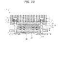
- the cover plate (the plate member) 23 may be provided between the bolster plate 2 and the main board 3 as depicted in FIG. 22 . That is, the cover plate 23 may be placed on the plate spring part 40 of the bolster plate 2.
- the main board 3 has a low stiffness, by applying a load from the plate spring part 40 of the bolster plate 2 to the main board 3, the main board 3 may be bent.
- partial concentration of the load applied from the plate spring part 40 of the bolster plate 2 to the main board 3 may be suppressed, and bending of the main board 3 may be suppressed.
- the cover plate 23 when the support 17 is provided to the outer peripheral portion of the upper surface of the bolster plate 2, the cover plate 23 may be placed on the support 17, as depicted in FIG. 23 .
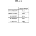
- Verification was performed regarding uniformity of the space between the main board 3 and the semiconductor package 5 in the electronic devices 1 according to the first, third, and fourth embodiments.
- the size of the semiconductor package 5 for verification was 40 cm 2
- the number of pins 21 of the LGA socket 4 was 3000
- the load that was applied to the main board 3 was 150 kg.
- verification was performed regarding uniformity of the space between the main board 52 and the semiconductor package 53 in the electronic device 51 according to the comparative example.
- the size of the semiconductor package 53 was 40 cm 2
- the number of pins of the LGA socket 55 was 3000
- the load to be applied to the main board 52 was 150 kg.
- the verification results are depicted in FIG. 24 .
- a numerical value in the field named "DIFFERENTIAL VALUE” is calculated by (maximum value of the space between the main board 3 and the semiconductor package 5) - (minimum value of the space between the main board 3 and the semiconductor package 5).
- Verification was performed for the uniformity of the space between the semiconductor package 5 and the base plate 11 in the electronic device 1 according to the third embodiment.
- the size of the semiconductor package 5 was 40 cm 2
- the number of pins 21 of the LGA socket 4 was 3000
- the load to be applied to the main board 3 was 150 kg.
- verification was performed for the uniformity of the space between the semiconductor package 53 and the base plate 58 in the electronic device 51 according to the comparative example.
- the size of the semiconductor package 53 was set at 40 cm 2
- the number of pins of the LGA socket 55 was 3000
- the load to be applied to the main board 52 was 150 kg.
- the electronic device 1 of the third embodiment depicted in FIG. 19 was used for verification.
- the electronic device 51 according to the comparative example a standard product was used for verification.
- the verification result was 0.05 mm.
- the verification result was 0.15 mm.
- the numerical value of the verification result for the third embodiment was calculated by (maximum value of the space between the semiconductor package 5 and the base plate 11) - (minimum value of the space between the semiconductor package 5 and the base plate 11).
- the numerical value of the verification result regarding the comparative example was calculated by (maximum value of the space between the semiconductor package 53 and the base plate 58) - (minimum value of the space between the semiconductor package 53 and the base plate 58). As such, it may be found that unevenness of the space between the semiconductor package 5 and the base plate 11 is more suppressed in the electronic device 1 according to the third embodiment, compared with the electronic device 51 according to the comparative example.
- the load to mount the semiconductor package 5 onto the main board 3 is increasing. According to the electronic devices 1 of the first to fourth embodiments, even if the load to mount the semiconductor package 5 on the main board 3 has increased, unevenness of the space between the main board 3 and the semiconductor package 5 may be suppressed. In addition, according to the electronic devices 1 of the first to fourth embodiments, even if the load to mount the semiconductor package 5 on the main board 3 has increased, unevenness of the space between the semiconductor package 5 and the base plate 11 may be suppressed.
- FIG. 25 is a cross-sectional view of the electronic device 1 when the semiconductor package 5 is mounted on the main board 3 with the BGA mounting methodology in the first embodiment. As depicted in FIG. 25 , solder balls 41 are placed on the lower surface of the semiconductor package 5. The solder balls 41 are an example of the connecting unit.
- the solder balls 41 and terminal electrodes provided to the lower surface of the semiconductor package 5 are bonded to each other.
- the bonding between the terminal electrodes provided to the lower surface of the semiconductor package 5 and the solder balls 41 are performed by melting the solder balls 41 with a reflow process.
- the terminal electrodes of the main board 3 and the solder balls 41 are bonded to each other.
- the bonding between the terminal electrodes of the main board 3 and the solder balls 41 are performed by melting the solder balls 41 with a reflow process.
- the solder balls 41 electrically couple the terminal electrodes of the main board 3 and the terminal electrodes of the semiconductor package 5 to each other. As a result, the main board 3 and the semiconductor package 5 are electrically coupled to each other via the solder balls 41.
- FIG. 26 is a cross-sectional view of the electronic device 1 when the semiconductor package 5 is mounted on the main board 3 with the PGA mounting methodology in the first embodiment.
- pins 42 are placed on the lower surface of the semiconductor package 5.
- the pins 42 are an example of the connecting unit. One ends of the pins 42 are coupled to the terminal electrodes provided to the lower surface of the semiconductor package 5.
- the other ends of the pins 42 are in contact with the terminal electrodes of the main board 3.
- the pins 42 electrically couple the terminal electrodes of the main board 3 and the terminal electrodes of the semiconductor package 5 to each other.
- the main board 3 and the semiconductor package 5 are electrically coupled to each other via the pins 42.
- the semiconductor package 5 is mounted on the main board 3.
- the first to fourth embodiments may be applied when the semiconductor chip 9 is mounted on the main board 3.
- the semiconductor chip 9 may be mounted on the main board 3, and the heat sink 6 may be placed on the semiconductor chip 9.
- a thermally conductive material such as aluminum, copper, or aluminum nitride may be interposed between the heat sink 6 and the semiconductor chip 9.
- the number of support shafts 13 to be placed is not restricted to four.
- the number of support shafts 13 to be placed may be two.
- the structures of the electronic devices 1 according to the first to fourth embodiments may be combined as much as possible.
Landscapes
- Cooling Or The Like Of Semiconductors Or Solid State Devices (AREA)
- Cooling Or The Like Of Electrical Apparatus (AREA)
Applications Claiming Priority (1)
| Application Number | Priority Date | Filing Date | Title |
|---|---|---|---|
| JP2011218289A JP2013077781A (ja) | 2011-09-30 | 2011-09-30 | 電子機器 |
Publications (1)
| Publication Number | Publication Date |
|---|---|
| EP2575168A1 true EP2575168A1 (de) | 2013-04-03 |
Family
ID=47071087
Family Applications (1)
| Application Number | Title | Priority Date | Filing Date |
|---|---|---|---|
| EP12181981A Withdrawn EP2575168A1 (de) | 2011-09-30 | 2012-08-28 | Elektronische Vorrichtung |
Country Status (3)
| Country | Link |
|---|---|
| US (1) | US20130083504A1 (de) |
| EP (1) | EP2575168A1 (de) |
| JP (1) | JP2013077781A (de) |
Cited By (1)
| Publication number | Priority date | Publication date | Assignee | Title |
|---|---|---|---|---|
| CN117174674A (zh) * | 2022-05-28 | 2023-12-05 | 华为技术有限公司 | 一种散热结构、车载设备及终端设备 |
Families Citing this family (10)
| Publication number | Priority date | Publication date | Assignee | Title |
|---|---|---|---|---|
| JP6135434B2 (ja) * | 2013-10-02 | 2017-05-31 | 富士通株式会社 | 冷却装置、電子機器および冷却装置の取付方法 |
| US10170391B2 (en) * | 2014-05-09 | 2019-01-01 | Lenovo Enterprise Solutions (Singapore) Pte. Ltd. | Backside initiated uniform heat sink loading |
| TWI544868B (zh) * | 2014-07-11 | 2016-08-01 | 台達電子工業股份有限公司 | 散熱模組及其結合方法 |
| JP6011667B2 (ja) * | 2015-03-20 | 2016-10-19 | 日本電気株式会社 | 冷却装置 |
| CN110637361B (zh) * | 2017-05-22 | 2024-04-19 | 索尼互动娱乐股份有限公司 | 电子设备 |
| US10616993B1 (en) * | 2018-01-15 | 2020-04-07 | Arista Networks, Inc. | Heatsink backing plate |
| JP7224146B2 (ja) * | 2018-11-02 | 2023-02-17 | 株式会社Pfu | 電子機器 |
| DE112019007624T5 (de) * | 2019-08-09 | 2022-04-21 | Mitsubishi Electric Corporation | Halbleitervorrichtung |
| CN112787118A (zh) * | 2019-11-08 | 2021-05-11 | 泰科电子(上海)有限公司 | 背板组件和电子装置 |
| US20230038805A1 (en) * | 2022-09-29 | 2023-02-09 | Intel Corporation | Methods, systems, apparatus, and articles of manufacture to control load distribution of integrated circuit packages |
Citations (8)
| Publication number | Priority date | Publication date | Assignee | Title |
|---|---|---|---|---|
| JPH03102365A (ja) | 1989-09-18 | 1991-04-26 | Ricoh Co Ltd | 作像装置 |
| JPH051285U (ja) | 1991-06-21 | 1993-01-08 | 埼玉日本電気株式会社 | 放熱プレート |
| US5473510A (en) * | 1994-03-25 | 1995-12-05 | Convex Computer Corporation | Land grid array package/circuit board assemblies and methods for constructing the same |
| US5528462A (en) * | 1994-06-29 | 1996-06-18 | Pendse; Rajendra D. | Direct chip connection using demountable flip chip package |
| JPH10173091A (ja) | 1996-12-12 | 1998-06-26 | Toshiba Corp | 半導体外囲器及び半導体装置 |
| JP3102365U (ja) * | 2003-12-18 | 2004-07-02 | 華▲孚▼科技股▲ふん▼有限公司 | ヒートシンク装置の留め具 |
| US20100053902A1 (en) * | 2008-09-01 | 2010-03-04 | Hon Hai Precision Industry Co., Ltd. | Electronic device with circuit board support |
| DE202010012950U1 (de) * | 2010-08-20 | 2011-02-24 | Micro-Star International Corp. Ltd., Jhonghe City | Befestigungsmechanismus zum Befestigen eines Thermomoduls an einer Basis und dazugehörige elektronische Vorrichtung |
Family Cites Families (5)
| Publication number | Priority date | Publication date | Assignee | Title |
|---|---|---|---|---|
| TW383955U (en) * | 1998-08-31 | 2000-03-01 | Hon Hai Prec Ind Co Ltd | Module apparatus for slot connector |
| US6386890B1 (en) * | 2001-03-12 | 2002-05-14 | International Business Machines Corporation | Printed circuit board to module mounting and interconnecting structure and method |
| JP3695376B2 (ja) * | 2001-09-28 | 2005-09-14 | 日本電気株式会社 | 回路基板の反り防止構造及び反り防止方法 |
| US7209354B2 (en) * | 2003-12-02 | 2007-04-24 | Silicon Intergrated Systems Corp. | Ball grid array package with heat sink device |
| JP2007305649A (ja) * | 2006-05-09 | 2007-11-22 | Matsushita Electric Ind Co Ltd | 放熱器固定手段 |
-
2011
- 2011-09-30 JP JP2011218289A patent/JP2013077781A/ja active Pending
-
2012
- 2012-08-16 US US13/587,268 patent/US20130083504A1/en not_active Abandoned
- 2012-08-28 EP EP12181981A patent/EP2575168A1/de not_active Withdrawn
Patent Citations (8)
| Publication number | Priority date | Publication date | Assignee | Title |
|---|---|---|---|---|
| JPH03102365A (ja) | 1989-09-18 | 1991-04-26 | Ricoh Co Ltd | 作像装置 |
| JPH051285U (ja) | 1991-06-21 | 1993-01-08 | 埼玉日本電気株式会社 | 放熱プレート |
| US5473510A (en) * | 1994-03-25 | 1995-12-05 | Convex Computer Corporation | Land grid array package/circuit board assemblies and methods for constructing the same |
| US5528462A (en) * | 1994-06-29 | 1996-06-18 | Pendse; Rajendra D. | Direct chip connection using demountable flip chip package |
| JPH10173091A (ja) | 1996-12-12 | 1998-06-26 | Toshiba Corp | 半導体外囲器及び半導体装置 |
| JP3102365U (ja) * | 2003-12-18 | 2004-07-02 | 華▲孚▼科技股▲ふん▼有限公司 | ヒートシンク装置の留め具 |
| US20100053902A1 (en) * | 2008-09-01 | 2010-03-04 | Hon Hai Precision Industry Co., Ltd. | Electronic device with circuit board support |
| DE202010012950U1 (de) * | 2010-08-20 | 2011-02-24 | Micro-Star International Corp. Ltd., Jhonghe City | Befestigungsmechanismus zum Befestigen eines Thermomoduls an einer Basis und dazugehörige elektronische Vorrichtung |
Cited By (2)
| Publication number | Priority date | Publication date | Assignee | Title |
|---|---|---|---|---|
| CN117174674A (zh) * | 2022-05-28 | 2023-12-05 | 华为技术有限公司 | 一种散热结构、车载设备及终端设备 |
| EP4525036A4 (de) * | 2022-05-28 | 2025-08-27 | Shenzhen Yinwang Intelligent Technology Co Ltd | Wärmeableitungsstruktur, fahrzeugmontierte vorrichtung und endgerätevorrichtung |
Also Published As
| Publication number | Publication date |
|---|---|
| US20130083504A1 (en) | 2013-04-04 |
| JP2013077781A (ja) | 2013-04-25 |
Similar Documents
| Publication | Publication Date | Title |
|---|---|---|
| EP2575168A1 (de) | Elektronische Vorrichtung | |
| US20060202325A1 (en) | Method and structure to provide balanced mechanical loading of devices in compressively loaded environments | |
| EP2770530A2 (de) | Elektronische Bauelementeinheit und Fixierstruktur | |
| JP6512644B1 (ja) | 放熱構造体、および放熱方法 | |
| US10892170B2 (en) | Fabricating an integrated circuit chip module with stiffening frame and orthogonal heat spreader | |
| CN1917189B (zh) | 模块化的散热器组件 | |
| US6545871B1 (en) | Apparatus for providing heat dissipation for a circuit element | |
| JP2004165586A (ja) | パッケージ構造、それを搭載したプリント基板、並びに、かかるプリント基板を有する電子機器 | |
| US8508031B2 (en) | Electronic device and method of producing the same | |
| KR19980063404A (ko) | 전자 패키지 조립체, 전자 패키지 조립체의 제조 방법 및 열전도성 구조체의 제조 방법 | |
| JP2013080742A (ja) | 半導体パッケージ、配線基板ユニット、及び電子機器 | |
| JP4910922B2 (ja) | 電子装置およびその製造方法 | |
| CN115866889A (zh) | 用于最佳xpu插槽压缩的改进的结构 | |
| US12500134B2 (en) | Package assembly including a package lid having a step region and method of making the same | |
| US7888790B2 (en) | Bare die package with displacement constraint | |
| US10607917B2 (en) | Substrate | |
| US7280360B2 (en) | Socket adapted for compressive loading | |
| JP2014002971A (ja) | コンタクト装置、ソケット装置及び電子装置 | |
| CN114334890B (zh) | 利用封装加强件将线缆组件附接到集成电路的装置、系统和方法 | |
| US20030003625A1 (en) | Leadframe pedestals for uniform die attach | |
| US20070149025A1 (en) | Substrate structure, substrate manufacturing method and electronic device | |
| JP2003037225A (ja) | 電子部品の冷却用熱伝導シート及び電子部品の冷却構造 | |
| CN104519721A (zh) | 冷却装置、电子设备和附接冷却装置的方法 | |
| JP5115270B2 (ja) | 半導体装置搭載基板及び半導体モジュール | |
| JP2000012735A (ja) | 半導体装置および半導体装置用補強板 |
Legal Events
| Date | Code | Title | Description |
|---|---|---|---|
| PUAI | Public reference made under article 153(3) epc to a published international application that has entered the european phase |
Free format text: ORIGINAL CODE: 0009012 |
|
| AK | Designated contracting states |
Kind code of ref document: A1 Designated state(s): AL AT BE BG CH CY CZ DE DK EE ES FI FR GB GR HR HU IE IS IT LI LT LU LV MC MK MT NL NO PL PT RO RS SE SI SK SM TR |
|
| AX | Request for extension of the european patent |
Extension state: BA ME |
|
| 17P | Request for examination filed |
Effective date: 20130730 |
|
| RBV | Designated contracting states (corrected) |
Designated state(s): AL AT BE BG CH CY CZ DE DK EE ES FI FR GB GR HR HU IE IS IT LI LT LU LV MC MK MT NL NO PL PT RO RS SE SI SK SM TR |
|
| STAA | Information on the status of an ep patent application or granted ep patent |
Free format text: STATUS: THE APPLICATION HAS BEEN WITHDRAWN |
|
| 18W | Application withdrawn |
Effective date: 20150603 |