EP2568658A2 - Kapazitative Kommunikationsschaltung und Verfahren dafür - Google Patents
Kapazitative Kommunikationsschaltung und Verfahren dafür Download PDFInfo
- Publication number
- EP2568658A2 EP2568658A2 EP12178622A EP12178622A EP2568658A2 EP 2568658 A2 EP2568658 A2 EP 2568658A2 EP 12178622 A EP12178622 A EP 12178622A EP 12178622 A EP12178622 A EP 12178622A EP 2568658 A2 EP2568658 A2 EP 2568658A2
- Authority
- EP
- European Patent Office
- Prior art keywords
- data signal
- signal
- capacitors
- circuit
- mixed
- Prior art date
- Legal status (The legal status is an assumption and is not a legal conclusion. Google has not performed a legal analysis and makes no representation as to the accuracy of the status listed.)
- Withdrawn
Links
Images


Classifications
-
- H—ELECTRICITY
- H04—ELECTRIC COMMUNICATION TECHNIQUE
- H04L—TRANSMISSION OF DIGITAL INFORMATION, e.g. TELEGRAPHIC COMMUNICATION
- H04L27/00—Modulated-carrier systems
-
- H—ELECTRICITY
- H04—ELECTRIC COMMUNICATION TECHNIQUE
- H04L—TRANSMISSION OF DIGITAL INFORMATION, e.g. TELEGRAPHIC COMMUNICATION
- H04L25/00—Baseband systems
- H04L25/02—Details ; arrangements for supplying electrical power along data transmission lines
- H04L25/0264—Arrangements for coupling to transmission lines
- H04L25/0266—Arrangements for providing Galvanic isolation, e.g. by means of magnetic or capacitive coupling
- H04L25/0268—Arrangements for providing Galvanic isolation, e.g. by means of magnetic or capacitive coupling with modulation and subsequent demodulation
-
- H—ELECTRICITY
- H04—ELECTRIC COMMUNICATION TECHNIQUE
- H04B—TRANSMISSION
- H04B5/00—Near-field transmission systems, e.g. inductive or capacitive transmission systems
- H04B5/20—Near-field transmission systems, e.g. inductive or capacitive transmission systems characterised by the transmission technique; characterised by the transmission medium
- H04B5/22—Capacitive coupling
-
- H—ELECTRICITY
- H04—ELECTRIC COMMUNICATION TECHNIQUE
- H04L—TRANSMISSION OF DIGITAL INFORMATION, e.g. TELEGRAPHIC COMMUNICATION
- H04L25/00—Baseband systems
- H04L25/02—Details ; arrangements for supplying electrical power along data transmission lines
Definitions
- circuit components use different types of power.
- applications such as electric vehicles, mains power supply, and motor drivers employ high voltage and low voltage domains, in which the low voltage domain may be used for controlling aspects of the high voltage domain.
- the respective domains are desirably isolated from each other, for safety reasons and/or to protect sensitive circuits from high voltages.
- Galvanic isolation allows the exchange of information between two parts of an electric circuit with separate grounds or two electric circuits without the actual flow of charge carriers between them.
- Galvanic isolation has been used in a variety of circuits, including those having different parts that operate at significantly different voltages in order to protect a lower voltage part, avoid unwanted ground loop bias, and achieve other desirable characteristics.
- An optocoupler circuit is one type of galvanic isolation circuit that has been employed to facilitate communications between circuits operating at different voltages.
- Optocouplers use light emitters and detectors (e.g ., a light emitting photodiode and a photodetector) that are respectively coupled to electrically isolated circuits, and are further electrically isolated from one another.
- Optocouplers and other isolation circuits can be useful, they can be relatively complex and added complexity/cost may be associated with interfacing transmitters and receivers. Optocouplers can also be sensitive to parameter variation, high power consumption and low bandwidth. Accordingly, the implementation of circuits requiring electrical and/or galvanic isolation continues to be challenging.
- Various example embodiments are directed to isolation circuits and approaches, and to addressing various challenges including those discussed above.
- capacitive signal communications are effected.
- An input signal is inverted, and both the inverted and non-inverted input signals are separately mixed (e.g ., modulated) with a carrier signal having a frequency that is different than the frequency of the input signal.
- the mixed signals are communicated capacitively over a circuit that passes frequencies of the carrier signal, facilitating undesirable coupling of signals of the input signal frequency, such as for isolating circuits operating at different voltages.
- Another example embodiment is directed to a communications circuit for communicating a digital data signal using a carrier signal having a frequency that is different than the frequency of the data signal, the communications circuit including sets of isolation capacitors and first and second circuits for passing the data signal.
- the first circuit uses the data signal and the carrier signal, generates mixed data signals respectively mixed with the carrier signal and an inverse of the carrier signal, and generates mixed inverted data signals respectively mixed with the carrier signal and an inverse of the carrier signal.
- the mixed data signals are provided to the first set of the isolation capacitors, and the mixed inverted data signals are provided to a second set of the isolation capacitors.
- the second circuit recovers the data signal from the mixed signals passed respectively via the first and second sets of capacitors.
- Another example embodiment is directed to a communications circuit having inversion circuits, a capacitive circuit including first and second sets of capacitors, and signal-mixing circuits.
- One of the inversion circuits inverts a data signal to provide an inverted data signal
- another one of the inversion circuits inverts a carrier signal to provide an inverted carrier signal, the carrier signal having a frequency that is different than the frequency of the data signal.
- the first signal-mixing circuit combines the data signal with at least one of the carrier signal and the inverted carrier signal, and thereby provides a combined data signal to the first set of capacitors.
- the first signal-mixing circuit also combines the inverted data signal with at least one of the carrier signal and the inverted carrier signal and thereby provides a combined inverted data signal to the second set of capacitors.
- the second signal-mixing circuit recovers the data signal from the combined data signal and the combined inverted data signal is passed respectively via the first and second sets of capacitors.
- Another example embodiment is directed to a method for communicating a digital data signal using a carrier signal having a frequency that is different than the frequency of the data signal.
- data signals are respectively mixed with the carrier signal and an inverse of the carrier signal
- inverted data signals are respectively mixed with the carrier signal and an inverse of the carrier signal.
- the mixed data signals are provided to a first set of capacitors
- the mixed inverted data signals are provided to a second set of capacitors.
- the data signal is recovered from the mixed signals passed respectively via the first and second sets of capacitors.
- the present invention is believed to be applicable to a variety of different types of circuits, devices and systems for and/or involving communications across a capacitive isolation barrier. While the present invention is not necessarily limited in this context, various aspects of the invention may be appreciated through a discussion of related examples.
- signal communications are effected capacitively, using an input signal and an inverted version of the input signal.
- Each of the respective input signal and inverted input signal is separately mixed (e.g ., modulated) with a carrier signal having a frequency that is different than the frequency of the input signal, as well as with an inverted version of the carrier signal.
- These mixed signals are communicated capacitively and the original input signal is recovered from the capacitive communication.
- circuits on transmission and receiving sides of the capacitive communication can be effectively isolated from one another, such as may be useful for isolating circuits operating at different voltages (e.g ., battery circuits), and where one voltage level of such a circuit could harm the other circuit.
- this approach can be implemented to provide immunity to voltage transients from one circuit to the other circuit.
- this approach can be used to accurately recover signals, as the various signals received via the capacitive communication for each respective mixed signal provide an accurate indication of rising and falling edges of the signals.
- this approach can be carried out without necessarily employing analog filtering at the receiving/recovery side of the communications.
- the capacitive communications are effected using pairs of capacitors.
- a first pair of capacitors includes capacitors respectively used to communicate the input signal as modulated with the carrier signal and with an inverted version of the carrier signal.
- a second pair of capacitors includes capacitors respectively used to communicate an inverted version of the input signal, as respectively modulated with the carrier signal and with an inverted version of the carrier signal. Accordingly, four signals are capacitively communicated and used to recover the input signal.
- pulses corresponding to the four signals are generated and used to recover the input signal. Pulses from each of the capacitors are consecutively-spaced during an active portion of the signal (e.g ., when the signal is positive for the first pair of capacitors, and when the signal is negative for the second pair of capacitors). For instance, the output of the first set of capacitors can be used to determine a rising edge of the data signal, and the output of the second set of capacitors can be used to determine a falling edge of the data signal.
- a first pulse of each series from the first pair of capacitors can be used as an indication of a rising edge of the signal
- a first pulse of each series from the second pair of capacitors can be used as an indication of a falling edge of the signal.
- a last pulse of each respective series may also be used to determine the rising and falling edges of the signal.
- the pulses are generated based upon a differential between the respective capacitors in each of the sets of capacitors.
- comparators can be used to compare a capacitive communication of the input signal mixed with the carrier signal, with a capacitive communication of the input signal mixed with the inverted carrier signal.
- Each comparator has its positive and negative input respectively coupled with different ones of the signals, each signal being coupled to a positive input of one of the comparators and to a negative input of the other one of the comparators.
- the capacitive communications can be effected to isolate or otherwise protect from the unwanted coupling of signals, in a variety of manners.
- a capacitive circuit as discussed above can be configured to pass high frequency signals, or low frequency signals, depending upon the particular application, the input signal type and the carrier signal type.
- the capacitive circuit includes resistors coupled to a voltage supply on the receiver side of the circuit, and configured with the capacitors to effect the passage of the carrier signal frequency.
- the resistors are used to make the receiver side impedance low. During voltage transient at either ground, the current will flow through the isolation capacitor. Because of the low impedance termination, the receiver side does not clip and the receiver continues to function, providing high common mode transient immunity.
- Another example embodiment is directed to a communications circuit having inversion circuits that respectively invert a data signal and a carrier signal having a frequency that is different than the frequency of the data signal.
- First and second signal-mixing circuits respectively transmit and receive communications using a capacitive circuit.
- the first signal-mixing circuit separately combines each of the data signal and the inverted data signal with at least one of the carrier signal and the inverted carrier signal, to provide outputs corresponding to each signal.
- the second signal-mixing circuit recovers the data signal from the combined data signal and the combined inverted data signal, which are passed respectively via the capacitive circuit.
- the first signal-mixing circuit may separately combine the data signal with each of the carrier signal and the inverted carrier signal to generate two mixed signals.
- the first signal-mixing circuit may separately combine the inverted data signal with each of the carrier signal and the inverted carrier signal to generate two additional mixed signals, corresponding to the inverted data signal.
- the passed signals can be processed using approaches as discussed above, such as by generating and using pulses corresponding to both the modulated data signal and the inverted modulated data signal.
- the data signal can be recovered using the pulses as an indication of a rising and/or falling edge of the data signal
- FIG. 1 shows a communications circuit 100 with capacitive isolation/communication components, in accordance with another example embodiment of the present invention.
- the circuit 100 includes, on a transmission side, two data signal modulator circuits 110 and 112, an oscillator 114 and an inverter circuit 116.
- a capacitive isolation circuit 120 separates the transmission side from a receiver side, the latter of which includes a data recovery circuit 130. Data input at the transmission side is processed and capacitively communicated, via the capacitive isolation circuit 120, to the receiver side.
- the data input signal is provided directly to the signal modulator circuit 110, and is first inverted via inverter circuit 116 before being provided to the signal modulator circuit 112.
- the oscillator 114 provides a carrier signal to each of the signal modulator circuits 110 and 112.
- Each of the respective signal modulator circuits 110 and 112 combines the received data signal or inverted data signal with an output of the oscillator, and provides outputs to the capacitive isolation circuit 120.
- the signal modulator circuits 110 and 112 respectively combine the data (or inverted data) signals provided thereto with the oscillator output and an inverted version of the oscillator output.
- the signal modulator circuits 110 and 112 may carry out the oscillator signal inversion, or the inversion may be carried out elsewhere ( e.g ., using an inverter circuit between the oscillator 114 and the signal modulator circuits).
- the capacitive isolation circuit 120 capacitively passes the outputs received from the signal modulator circuits 110 and 112, to the data recovery circuit 130.
- the respective signals are processed at the data recovery circuit to generate pulses that are used to determine rising and falling edges for reconstruction of the original input signal.
- first and last ones of a series of consecutive pulses from the data signal modulator 110 can be used as an indication of the start and end of a positive segment of the input signal.
- first and last pulses of a series of consecutive pulses from the data signal modulator 112 can respectively be used as an indication of the end and start of the positive segment of the input signal.
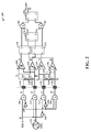
- Figure 2 shows a capacitive communications circuit 200 for communicating an input signal to an output over a capacitive circuit.
- the circuit 200 includes several AND gates 210, 212, 214 and 216, respectively coupled to receive an input data signal (at B) and an oscillator signal from oscillator 220.
- Inverter circuits 230 and 234 respectively invert the oscillator signal provided to the AND gates 210 and 214.
- Inverter circuit 236 inverts the input data signal and provides the inverted input data signal to the AND gates 214 and 216.
- the outputs of the AND gates 210, 212, 214 and 216 are respectively provided to isolation capacitors 240, 242, 244 and 246.
- the capacitors 240, 242, 244 and 246 are connected to provide outputs to a plurality of comparators 250, 252, 254 and 256, with the signals provided thereto being generated via resistors 260, 262, 264 and 266, and V ref coupled thereto as shown.
- Each of the comparators 250 and 252 has two inputs respectively coupled to an output of the capacitors 240 and 242 as shown, alternating at the positive and negative inputs thereof.
- each of the comparators 254 and 256 has two inputs respectively coupled to an output of the capacitors 244 and 246 as shown.
- comparators 250 and 256 are respectively coupled to the set and reset inputs of flip-flop 270, and the outputs of comparators 252 and 254 are respectively coupled to the set and reset inputs of flip-flop 272. Accordingly, the outputs corresponding to input signal are provided to the respective set inputs, and the outputs corresponding to the inverted input signal are provided to the respective reset inputs.
- the receiver side of the circuit 200 also includes a third flip-flop 274, AND gates 280 and 282, and a fourth flip-flop 290.
- the outputs of the flip-flop 270 are respectively provided to the AND gate 280 and the reset input of the flip-flop 274, an output of which is also provided to the AND gate 280.
- the outputs of flip-flop 272 are respectively provided to the AND gate 282 and the set input of flip-flop 274, an output of which is also provided to the AND gate 282.
- the outputs of the AND gates 280 and 282 are respectively provided to reset and set inputs of the flip-flop 290, the output of which corresponds to the recovered input signal.
- the AND gates 210, 212, 214 and 216 respectively mix, or modulate, the input signal and an inverted version of the input signal with the oscillator signal and an inverted version of the oscillator signal.
- This combination of signals provides outputs at the capacitive circuits 240, 242, 244 and 246 that correspond to respective series of pulses indicative of rising and falling edges of the input signal.
- the receiver side of the circuit processes the pulses to (effectively) identify rising and falling edges of the recovered signal and, correspondingly, provide the output at flip-flop 290 corresponding to the input signal.
- Figure 3 is a signal diagram showing exemplary signals corresponding to the operation of a capacitive isolation circuit, in accordance with another example embodiment of the present invention.
- the signal diagram in Figure 3 may be implemented with a circuit as shown in Figure 2 , or with similar circuits configured for communicating capacitive signals as discussed herein.
- Figure 2 shows corresponding references to the indicated signals in Figure 3 .
- signal A is an output signal from the oscillator 220
- signal B is the input signal
- signal O is the output signal.
- Signals C and D correspond respectively to the input signal modulated with the inverted oscillator signal, and a corresponding capacitive output.
- Signals C and D correspond respectively to the input signal modulated with the oscillator signal, and a corresponding capacitive output.
- Signals F and G correspond respectively to the inverted input signal modulated with the inverted oscillator signal, and a corresponding capacitive output.
- Signals F and G correspond respectively to the inverted input signal modulated with the oscillator signal, and a corresponding capacitive output.
- Signals E and E correspond respectively outputs of comparators 250 and 252, as pulses for the non-inverted input signal.
- Signals H and H correspond respectively outputs of comparators 254 and 256, as pulses for the inverted input signal. These signals are processed at the flip-flops 270, 272, 274 and 290, as well as at AND gates 280 and 282, to produce the output signal O.
- the signal transfer across the isolation capacitor in the proposed embodiment is thus based on the polarity of the data signal. Assuming, by way of example, that the oscillator frequency is higher than the maximum data rate, an incoming bit stream at B is modulated with a square wave oscillator signal A, and the modulated signal is transferred across the upper differential pair of isolation capacitors 240 and 242. Similarly the inverted incoming bit stream is modulated with the oscillator signal A and transferred across the lower differential pair of isolation capacitors 244 and 246.
- the isolation capacitors and the termination resistance (260, 262, 264, 266) at the receiving node acts as a high pass filter for the incoming signals C, C , F and F . Comparators 250, 252, 254 and 256 at the receiving end convert the incoming signals into short output pulses as shown in Figure 3 .
- the start of a short pulse coincides with the rising edge of the data signal.
- the start of the short pulse coincides with the falling edge of the data signal.
- the start of these short pulses is used to detect the rising and falling edge of the data in recovering/generating the output signal, facilitating a low propagation delay and pulse width distortion. Referring to time periods represented at 310, 320 and 330, the start of a first one of a series of consecutively-spaced short pulses occurring during time period 310 can be used as an indication of a rising edge of the data signal.
- the aforesaid short pulses (at node E or E ) are not present, with the start of another series of consecutively-spaced short pulses (at node H or H) being indicative of a falling edge of the data signal.
- another series of short pulses (at node E or E ) begins and is again indicative of the rising edge of the data signal.
- Figure 3 shows a specific implementation, other approaches may be used with alternate combinations of inverted signals, with different frequencies, and with different recovery/output generation approaches.
- the falling edge of a last one of the pulses (at node E or E ) with time periods 310 and 330 as discussed above can be used as an indication of the falling edge of the data signal, in lieu of and/or in addition to using a rising edge of a first one of the pulses in time period 320 (at node H or H ).
- the falling edge of a last one of the pulses (at node H or H ) in time period 320 can be used as an indication of the rising edge of the data signal in transitioning from time period 320 to 330.
Landscapes
- Engineering & Computer Science (AREA)
- Computer Networks & Wireless Communication (AREA)
- Signal Processing (AREA)
- Power Engineering (AREA)
- Dc Digital Transmission (AREA)
- Near-Field Transmission Systems (AREA)
Applications Claiming Priority (1)
| Application Number | Priority Date | Filing Date | Title |
|---|---|---|---|
| US13/230,134 US8693554B2 (en) | 2011-09-12 | 2011-09-12 | Capacitive communication circuit and method therefor |
Publications (2)
| Publication Number | Publication Date |
|---|---|
| EP2568658A2 true EP2568658A2 (de) | 2013-03-13 |
| EP2568658A3 EP2568658A3 (de) | 2017-08-09 |
Family
ID=46796272
Family Applications (1)
| Application Number | Title | Priority Date | Filing Date |
|---|---|---|---|
| EP12178622.2A Withdrawn EP2568658A3 (de) | 2011-09-12 | 2012-07-31 | Kapazitative Kommunikationsschaltung und Verfahren dafür |
Country Status (5)
| Country | Link |
|---|---|
| US (1) | US8693554B2 (de) |
| EP (1) | EP2568658A3 (de) |
| JP (1) | JP5518153B2 (de) |
| KR (1) | KR101457268B1 (de) |
| CN (1) | CN103001897B (de) |
Families Citing this family (5)
| Publication number | Priority date | Publication date | Assignee | Title |
|---|---|---|---|---|
| KR102252834B1 (ko) * | 2015-08-07 | 2021-05-18 | 엠텍비젼 주식회사 | 커패시티브 통신에서 m-phy의 모든 신호레벨을 전달하기 위한 시스템 |
| US9935763B2 (en) * | 2016-06-17 | 2018-04-03 | Texas Instruments Incorporated | Timing correction in a communication system |
| CN106341164B (zh) * | 2016-10-18 | 2018-08-17 | 深圳市阿美特科技有限公司 | 低功耗近距离无线通信电路 |
| EP3598409B1 (de) * | 2018-07-16 | 2021-03-10 | Melexis Technologies NV | Sende-empfänger mit mitteln zur galvanischen isolation |
| US20250202528A1 (en) * | 2023-12-18 | 2025-06-19 | Infineon Technologies Austria Ag | Capacitive communication system and configuration |
Family Cites Families (16)
| Publication number | Priority date | Publication date | Assignee | Title |
|---|---|---|---|---|
| US3038960A (en) * | 1960-06-27 | 1962-06-12 | Peter G S Mero | Recording devices |
| US4142205A (en) * | 1976-07-21 | 1979-02-27 | Nippon Electric Co., Ltd. | Interframe CODEC for composite color TV signals comprising means for inverting the polarity of carrier chrominance signals in every other frame or line |
| US4245355A (en) * | 1979-08-08 | 1981-01-13 | Eaton Corporation | Microwave frequency converter |
| US4298986A (en) * | 1979-12-26 | 1981-11-03 | General Electric Company | Receiver for phase-shift modulated carrier signals |
| US5500895A (en) * | 1994-05-24 | 1996-03-19 | Yurgelites; Gerald J. | Telephone isolation device |
| US5781588A (en) * | 1994-11-10 | 1998-07-14 | Matsushita Electric Industrial Co., Ltd. | FSK signal receiver |
| US5949826A (en) * | 1995-12-22 | 1999-09-07 | Matsushita Electric Industrial Co., Ltd. | Data transmission and reception system |
| GB9605719D0 (en) * | 1996-03-19 | 1996-05-22 | Philips Electronics Nv | Integrated receiver |
| US6058191A (en) | 1997-02-04 | 2000-05-02 | Macrovision Corp | Method and apparatus for modifying the envelope of a RF carrier signal to remove copy protection signals therefrom |
| US6339048B1 (en) * | 1999-12-23 | 2002-01-15 | Elementis Specialties, Inc. | Oil and oil invert emulsion drilling fluids with improved anti-settling properties |
| US6366229B2 (en) * | 1999-01-06 | 2002-04-02 | Raytheon Company | System for continuous-time modulation |
| FR2799912B1 (fr) * | 1999-10-19 | 2002-02-15 | St Microelectronics Sa | Transmission d'une horloge par une barriere d'isolement capacitive |
| KR100689033B1 (ko) * | 2001-02-02 | 2007-03-08 | 삼성전자주식회사 | 데이터 슬라이서 및 이를 적용한 알에프 수신기 |
| CN100531357C (zh) * | 2004-05-12 | 2009-08-19 | 韩国电子通信研究院 | 用于同频转发器中的对应频率同步的设备和方法 |
| US8198951B2 (en) * | 2004-06-03 | 2012-06-12 | Silicon Laboratories Inc. | Capacitive isolation circuitry |
| US7956510B2 (en) * | 2006-04-04 | 2011-06-07 | Kolo Technologies, Inc. | Modulation in micromachined ultrasonic transducers |
-
2011
- 2011-09-12 US US13/230,134 patent/US8693554B2/en active Active
-
2012
- 2012-07-31 EP EP12178622.2A patent/EP2568658A3/de not_active Withdrawn
- 2012-09-06 JP JP2012196596A patent/JP5518153B2/ja active Active
- 2012-09-07 CN CN201210330305.XA patent/CN103001897B/zh active Active
- 2012-09-12 KR KR1020120101262A patent/KR101457268B1/ko active Active
Non-Patent Citations (1)
| Title |
|---|
| None |
Also Published As
| Publication number | Publication date |
|---|---|
| US20130064310A1 (en) | 2013-03-14 |
| CN103001897A (zh) | 2013-03-27 |
| CN103001897B (zh) | 2015-04-08 |
| KR20130028889A (ko) | 2013-03-20 |
| JP5518153B2 (ja) | 2014-06-11 |
| EP2568658A3 (de) | 2017-08-09 |
| JP2013062797A (ja) | 2013-04-04 |
| KR101457268B1 (ko) | 2014-10-31 |
| US8693554B2 (en) | 2014-04-08 |
Similar Documents
| Publication | Publication Date | Title |
|---|---|---|
| US8798175B2 (en) | Communicating with a self-clocking amplitude modulated signal | |
| US8576928B2 (en) | Capacitive divider transmission scheme for improved communications isolation | |
| CN105429624B (zh) | 信号隔离器系统中的开关键调制信号的解调 | |
| US8867592B2 (en) | Capacitive isolated voltage domains | |
| US8693554B2 (en) | Capacitive communication circuit and method therefor | |
| US9396871B2 (en) | Signal transmitting circuit | |
| JP5543402B2 (ja) | リンギング抑制回路 | |
| US20220308618A1 (en) | Clock data recovery circuit | |
| US8817670B2 (en) | Full duplex communication circuit and method therefor | |
| CN115549659A (zh) | 发射器电路、对应隔离驱动设备、电子系统以及方法 | |
| US20120081177A1 (en) | Signal Transmission Arrangement with a Transformer and Signal Transmission Method | |
| TWI514828B (zh) | 用於傳輸振幅調變信號的方法,傳輸器,菊鏈通信系統以及積體電路 | |
| WO2013100005A1 (ja) | 通信システム、半導体駆動装置及び電力変換装置 | |
| CN210246716U (zh) | 一种隔离式信号传输电路及利用其的通信装置 | |
| Ke et al. | Design of capacitive digital isolation chip | |
| US12537522B2 (en) | Isolated driver device, corresponding electronic system and method of transmitting a data signal across a galvanic isolation barrier | |
| CN114982134A (zh) | 快速数字隔离器 | |
| CN115622853A (zh) | 单总线通信调制解调电路及芯片 | |
| CN104038191A (zh) | 电压型栅控器件的驱动电路 | |
| CN116743118B (zh) | 信号整形电路和数字电容隔离器 | |
| KR102028391B1 (ko) | 신호절연회로 | |
| US20260113030A1 (en) | Isolated driver device, corresponding electronic system and method of transmitting a data signal across a galvanic isolation barrier | |
| JP2020031272A (ja) | 半導体装置 |
Legal Events
| Date | Code | Title | Description |
|---|---|---|---|
| PUAI | Public reference made under article 153(3) epc to a published international application that has entered the european phase |
Free format text: ORIGINAL CODE: 0009012 |
|
| AK | Designated contracting states |
Kind code of ref document: A2 Designated state(s): AL AT BE BG CH CY CZ DE DK EE ES FI FR GB GR HR HU IE IS IT LI LT LU LV MC MK MT NL NO PL PT RO RS SE SI SK SM TR |
|
| AX | Request for extension of the european patent |
Extension state: BA ME |
|
| 17P | Request for examination filed |
Effective date: 20140331 |
|
| RAP1 | Party data changed (applicant data changed or rights of an application transferred) |
Owner name: NXP B.V. |
|
| PUAL | Search report despatched |
Free format text: ORIGINAL CODE: 0009013 |
|
| AK | Designated contracting states |
Kind code of ref document: A3 Designated state(s): AL AT BE BG CH CY CZ DE DK EE ES FI FR GB GR HR HU IE IS IT LI LT LU LV MC MK MT NL NO PL PT RO RS SE SI SK SM TR |
|
| AX | Request for extension of the european patent |
Extension state: BA ME |
|
| RIC1 | Information provided on ipc code assigned before grant |
Ipc: H04L 12/12 20060101AFI20170706BHEP Ipc: H04L 25/02 20060101ALI20170706BHEP |
|
| RBV | Designated contracting states (corrected) |
Designated state(s): AL AT BE BG CH CY CZ DE DK EE ES FI FR GB GR HR HU IE IS IT LI LT LU LV MC MK MT NL NO PL PT RO RS SE SI SK SM TR |
|
| STAA | Information on the status of an ep patent application or granted ep patent |
Free format text: STATUS: REQUEST FOR EXAMINATION WAS MADE |
|
| STAA | Information on the status of an ep patent application or granted ep patent |
Free format text: STATUS: THE APPLICATION IS DEEMED TO BE WITHDRAWN |
|
| 18D | Application deemed to be withdrawn |
Effective date: 20180210 |