EP2567458B1 - Rauschunterdrückung für differenzialverstärker ohne erforderlichen externen abgleich - Google Patents
Rauschunterdrückung für differenzialverstärker ohne erforderlichen externen abgleich Download PDFInfo
- Publication number
- EP2567458B1 EP2567458B1 EP11721865.1A EP11721865A EP2567458B1 EP 2567458 B1 EP2567458 B1 EP 2567458B1 EP 11721865 A EP11721865 A EP 11721865A EP 2567458 B1 EP2567458 B1 EP 2567458B1
- Authority
- EP
- European Patent Office
- Prior art keywords
- input
- amplifier
- complementary
- output
- coupled
- Prior art date
- Legal status (The legal status is an assumption and is not a legal conclusion. Google has not performed a legal analysis and makes no representation as to the accuracy of the status listed.)
- Active
Links
Images


Classifications
-
- H—ELECTRICITY
- H03—ELECTRONIC CIRCUITRY
- H03F—AMPLIFIERS
- H03F3/00—Amplifiers with only discharge tubes or only semiconductor devices as amplifying elements
- H03F3/30—Single-ended push-pull [SEPP] amplifiers; Phase-splitters therefor
- H03F3/3081—Duplicated single-ended push-pull arrangements, i.e. bridge circuits
-
- H—ELECTRICITY
- H03—ELECTRONIC CIRCUITRY
- H03F—AMPLIFIERS
- H03F3/00—Amplifiers with only discharge tubes or only semiconductor devices as amplifying elements
- H03F3/30—Single-ended push-pull [SEPP] amplifiers; Phase-splitters therefor
-
- H—ELECTRICITY
- H03—ELECTRONIC CIRCUITRY
- H03F—AMPLIFIERS
- H03F3/00—Amplifiers with only discharge tubes or only semiconductor devices as amplifying elements
- H03F3/189—High-frequency amplifiers, e.g. radio frequency amplifiers
Definitions
- the disclosed embodiments relate to differential amplifiers, and more particularly to high performance differential amplifiers that can be coupled to low impedance sources without intervening matching networks.
- FIG. 1 is a simplified block diagram of a device that employs such an LNA.
- the device is a mobile communication device (for example, a cellular telephone handset) and includes an antenna 1, an analog Radio Frequency (RF) transceiver integrated circuit 2, a digital baseband processor integrated circuit 3, a duplexer 4, a power amplifier 5, and a number of matching networks 6-9.
- RF Radio Frequency
- a processor 10 in the digital baseband processor integrated circuit 3 controls the RF transceiver 2 by sending control communications to a receive chain 11 and to a transmit chain 12 of the RF transceiver integrated circuit 2 via a serial bus 13.
- the first stage of the receive chain 11 is the LNA 14.
- FIG. 2 is a more detailed diagram of the portion of the circuit of FIG. 1 between antenna 1 and LNA 14.
- the LNA in this example is a differential LNA.
- LNA 14 receives a differential signal via terminals 15 and 16. Dashed line 17 represents the boundary of integrated circuit 2.
- LNA 14 outputs a differential signal to a differential quadrature mixer circuit 18.
- the receiver is tuned by setting the frequency of a local oscillator signal LO1 output by a local oscillator 19.
- the signal input path to the terminals 15 and 16 includes antenna 1, matching network 6, duplexer 4, a bandpass filter (BPF) 20, a balun 21, and matching network 7. Providing the additional components of matching network 7 generally adds cost to the manufacturing cost of the overall device.
- BPF bandpass filter
- the input impedance at operational frequencies looking into the conventional LNA 14 of FIG. 2 is substantially higher than fifty ohms and may be one hundred ohms or more.
- the impedance of antenna 1, on the other hand, is approximately fifty ohms.
- FIGS. 3-6 are diagrams of several conventional types of LNAs. Although single-ended examples of the topologies are presented for ease of illustration and explanation, the topologies are extendable to differential circuits.
- FIG. 3 is a diagram of an LNA having a resistive feedback amplifier based input stage and a source follower based output stage.
- Transistors M 1a and M 1b and resistor R form the input stage.
- Transistors M 2a and M 2b and M 3 form the output stage.
- IN denotes the input node.
- OUT denotes the output node.
- This LNA circuit has an advantage that noise and distortion products of the input stage including the noise of resistor R are substantially canceled.
- the noise on nodes X and Y is, however, in phase.
- a source follower output stage is employed.
- the source of transistor M 3 is coupled to the output node OUT.
- the output impedance of the LNA is low and gain is limited.
- FIG. 4 is a diagram of another conventional single-ended LNA that includes a resistive feedback input stage and a source follower output stage. Circuit components 22, 23 and 24 form the resistive feedback input stage. Circuit components 25, 26 and 27 form a source follower output stage. In this case, as in the case of the circuit of FIG. 3 , noise of the feedback resistor 23 is substantially canceled.
- the source follower output stage provides rather limited gain.
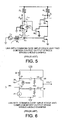
- FIG. 5 is a diagram of an LNA having a common-gate input stage and two common source output stages.
- Transistor M 1 and resistor R 1 form the input stage.
- Transistors M 3 and M 5 and resistor R L form the first output stage.
- Transistors M 4 and M 5 and resistor R L form the second output stage.
- This circuit has the advantage of relatively high gain and has the advantage that noise and distortion products of transistor M 1 of the input stage are canceled.
- a disadvantage, however, is that noise from resistor R 1 is not canceled.
- the resistance of R 1 is limited by available voltage headroom. There is a need for a current source at the input of the common gate input amplifier, but the noise of this current source is not canceled.
- FIG. 6 is a diagram of yet another conventional LNA.
- This LNA includes a common-gate input stage as in the case of the LNA of FIG. 5 .
- the input stage involves circuit components 28, 29 and 30. Noise of load resistor 30 is not canceled.
- the LNA of FIG. 6 includes a complementary output stage and has an advantage of high gain.
- the term complementary is used to indicate that the output stage includes a P-channel transistor 31 as well as an N-channel transistor 32.
- a differential Low Noise Amplifier includes a first stage of resistive feedback amplifiers and second stage of complementary amplifiers, where the outputs of the first stage are coupled to the inputs of the second stage in a cross-coupled fashion.
- An inductive load (such as a transformer load) combines signals output from the complementary amplifiers of the second stage.
- the LNA has an input impedance of less than 75 ohms, a noise factor of less than 2 dB, and a gain of more than 20 dB. Due to the low input impedance, the LNA is usable to amplify a signal received from a source having a similar low impedance without the use of an impedance matching network between the output of the source and the input of the LNA.
- a differential LNA has a first LNA input node and a second LNA input node.
- a first resistive feedback amplifier receives a first signal from the first LNA input node and supplies an amplified version of the first signal to a first input of a second complementary amplifier. The first signal is also supplied onto a second input of a first complementary amplifier.
- a second resistive feedback amplifier receives a second signal from the second LNA input node and supplies an amplified version of the second signal to a first input of the first complementary amplifier. The second signal is also supplied onto a second input of the second complementary amplifier.
- the first and second signals on the LNA input nodes together are a differential LNA input signal.
- Output signals from the first and second complementary amplifiers are supplied onto two corresponding terminals of a primary winding of a transformer load.
- a secondary winding of the transformer load supplies a differential LNA output signal onto a pair of LNA output nodes.
- the differential LNA has an input impedance of less than 75 ohms, a noise factor of less than 2 dB, and a gain of more than 20 dB, when the differential LNA input signal has a frequency in a frequency range of from 100 MHz to 2.0 GHz.
- FIG. 7 is a very simplified high level block diagram of one exemplary system that includes a Low Noise Amplifier (LNA) 100 in accordance with one novel aspect.
- the system is a mobile communication device 101 such as a cellular telephone.
- Device 101 includes (among other parts not illustrated) an antenna 102 usable for receiving and transmitting cellular telephone communications, an RF transceiver integrated circuit 103, and a digital baseband processor integrated circuit 104.
- FIG. 8 is a more detailed diagram of the RF transceiver integrated circuit 103 of FIG. 7 .
- the incoming signal passes through a matching network 106, a duplexer 107, a bandpass filter 108, a balun 109, and into RF transceiver integrated circuit 103 via terminals 110 and 111.
- the functions of BPF 108 and balun 109 are accomplished using a SAW filter.
- the incoming signal is amplified by LNA 100.
- LNA 100 is part of a receive chain 112.
- the information After being downconverted in frequency by a quadrature mixer 113 and after being filtered by baseband filter 114, the information is communicated to the digital baseband processor integrated circuit 104 for analog-to-digital conversion and further processing in the digital domain. How the receive chain downconverts is controlled by changing the frequency of a local oscillator signal LO1 generated by local oscillator 115.
- the audio information to be transmitted is converted into analog form in digital baseband processor integrated circuit 104.
- the analog information is supplied to a baseband filter 116 of a transmit chain 117 of RF transceiver integrated circuit 103.
- the signal is upconverted in frequency by quadrature mixer 118.
- the upconversion process is tuned and controlled by controlling the frequency of a local oscillator signal LO2 generated by local oscillator 119.
- the resulting upconverted signal is amplified by a driver amplifier 120 and is output from the RF transceiver integrated circuit 103 via terminals 121.
- the signal passes through a matching network 122 and is amplified by an external power amplifier 123.
- the amplified signal passes through another matching network 124, and duplexer 107 and matching network 106 is supplied onto antenna 102 for transmission as outgoing transmission 125.
- the local oscillators 115 and 119 of the receive and transmit chains are controlled by control information received via bus interface 126, serial bus 127, bus interface 128, and control conductors 129 and 130.
- the control information is generated by a processor 131 executing a set of processor-executable instructions 132.
- the instructions are stored in a processor-readable medium 133.
- FIG. 9 is a more detailed diagram of a part of the receive signal path of the circuit of FIG. 8 .
- Mixer 113 is a quadrature mixer and is shown in symbolic form in FIG. 9 .
- Mixer 113 receives a differential In-phase (I) signal and a differential Quadrature (Q) signal from local oscillator 115.
- Mixer 113 receives a differential LNA output signal via LNA output conductors 134 and 135. This differential LNA output signal involves the signal LNAOUTP on conductor 134 and the signal LNAOUTN on conductor 135.
- LNA 100 receives a differential LNA input signal via LNA input conductors 136 and 137.
- This differential LNA input signal involves the signal LNAINP on conductor 136 and terminal 110 and also involves the signal LNAINN on conductor 137 and terminal 111.
- Dashed line 138 represents the boundary of the RF integrated circuit 103.
- Terminals 110 and 111 may, for example, be terminals of an integrated circuit package that houses RF transceiver integrated circuit 103.
- Terminals 110 and 111 may, for example, be microbumps or bond pads of RF transceiver integrated circuit 103.
- the input impedance looking into RF transceiver integrated circuit 103 through terminals 110 and 111 and conductors 136 and 137 is approximately 50 ohms and is less than 75 ohms.
- a first ESD protection circuit 186 also loads conductor 136 with 50fF of capacitance.
- Conductors 139 and 140 are conductors such as traces on a printed circuit board extending from balun 109 to the RF transceiver integrated circuit 103.
- Conductor 139, terminal 110, and conductor 136 together form a first input node.
- a second ESD protection circuit 187 also loads conductor 137 with 50fF of capacitance.
- Conductor 140, terminal 111, and conductor 137 together form a second input node.
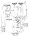
- FIG. 10 is a more detailed diagram of LNA 100 of FIG. 9 .
- LNA 100 includes a first resistive feedback inverting amplifier 141, a second resistive feedback inverting amplifier 142, a first complementary output stage amplifier 143, a second complementary output stage amplifier 144, an inductive load 145, and a biasing circuit.
- the biasing circuit includes resistors 150 and 151, reference voltage source 152 of magnitude VREF, operational amplifier 153, and P-channel transistor 154.
- the biasing circuit sets a common mode voltage of a differential output signal present between nodes 174 and 175.
- the magnitude of VREF is set or is adjusted to optimize the linearity performance of the LNA.
- First feedback inverting amplifier 141 includes a feedback resistance 155 and an amplifier 156.
- Second feedback inverting amplifier 142 includes a feedback resistance 157 and an amplifier 158.
- Inverting amplifiers 156 and 158 need not be implemented as complementary logic gate inverters (involving a P-channel pullup and an N-channel pulldown) but rather may be implemented in numerous ways. The inverter symbol is intended to be general representation of an inverting amplifier.
- First complementary output stage amplifier 143 includes a P-channel field effect transistor 159 and an N-channel field effect transistor 160.
- second complementary output stage amplifier 144 includes a P-channel field effect transistor 161 and an N-channel field effect transistor 162.
- Inductive load 145 in this example is a tuned transformer load and includes a first winding 163 and a second winding 164.
- First winding 163 has a first terminal 165, a second terminal 166, and a center tap terminal 167.
- First winding 163 may, for example, be an integrated spiral metal inductor realized in upper layers of metallization and interlayer vias so that winding 163 has two to four turns and has an inductance of about 2nH.
- the biasing circuit is connected to center tap terminal 167 of winding 163 via P-channel transistor 154.
- An input 168 of the first resistive feedback amplifier 141 is coupled to conductor 136, to terminal 110, and to the gate of N-channel transistor 160 of the first complementary output stage amplifier 143.
- An input 169 of the second resistive feedback amplifier 142 is coupled to conductor 137, to terminal 111, and to the gate of N-channel transistor 162 of the second complementary output stage amplifier 144.
- the output 170 of the first resistive feedback amplifier 141 is capacitively coupled via capacitance 171 to the gate of the P-channel transistor of the second complementary output stage amplifier 144.
- the output 172 of the second resistive feedback amplifier 142 is capacitively coupled via capacitance 173 to the gate of the P-channel transistor of the first complementary output stage amplifier 143.
- the gate of P-channel transistor 159 is a first input to first complementary output stage amplifier 143 and the gate of N-channel transistor 160 is a second input to first complementary output stage amplifier 143 and node 174 at the drains of transistors 159 and 160 is the output first complementary output stage amplifier 143.
- the gate of P-channel transistor 161 is a first input to second complementary output stage amplifier 144 and the gate of N-channel transistor 162 is a second input to second complementary output stage amplifier 144 and node 175 at the drains of transistors 161 and 162 is the output of second complementary output stage amplifier 144.
- the second winding 164 of transformer load 145 is tuned by capacitor 176.
- Terminal 177 on second winding 164 is capacitively coupled via capacitance 178 to output conductor 134.
- Terminal 179 on second winding 164 is capacitively coupled via capacitance 180 to output conductor 135.
- Conductor 181 is a supply voltage conductor VDD.
- Conductor 182 is a ground conductor GND.
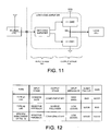
- FIG. 11 is a diagram that represents a simplification of the composition of the conventional LNAs of FIG. 3-6 and of the LNA 100 of FIG. 10 .
- the LNAs have an input stage 183, also referred to as a matching amplifier, as well as an output stage 184.
- the outputs of the amplifiers of the second stage are added together as represented by node 185.
- the conventional LNAs of FIGS. 3-6 can be classified into two general types. In the first type of LNA, designated TYPE#1 here, the input stage is a common-gate amplifier.
- the LNA of FIG. 6 is an example of such an LNA.
- Voltage noise on one of the output nodes 33 of the first stage is out of phase with respect to voltage noise on the other of the output nodes 34 of the first stage.
- a complementary output stage can be used to add such signals, thereby effectively canceling out of phase components of the signals.
- this noise is canceled by the complementary output stage and does not pass to the output of the LNA.
- LNAs of this type can have a high voltage gain due to the output impedance of the output stage being high. Noise of the load resistance 30 of the input stage going into the output stage is, however, not out of phase. Noise on nodes 33 and 34 due to load resistance 30 therefore passes through the output stage without being canceled.
- the input stage involves a resistive feedback amplifier.
- the LNA of FIG. 3 is an example of such an LNA.
- Noise due to resistance R of the input stage is in phase on the output nodes X and Y of the first stage.
- the output stage of the LNA is, however, of a type that subtracts common mode signals on the outputs of the first stage. Resistor noise on node X is therefore effectively subtracted from resistor noise on node Y.
- noise factor of TYPE#2 LNAs is generally comparatively good.
- Gain, however, of this TYPE#2 LNA is comparatively bad.
- gain is low because the impedance looking into the LNA through node OUT is low.
- the output impedance is low because the source of a transistor, N-channel transistor M 3 , is coupled to node OUT.
- the table of FIG. 12 is created and studied. It is recognized that the best choice for the input stage in a two stage LNA is a resistive feedback amplifier because a resistive feedback amplifier gives the best noise factor. It is further recognized that the best choice for the output stage is a complementary amplifier because a complementary amplifier gives the best gain due to the fact that no transistor source is coupled to the output node. However, if a resistive feedback amplifier is used as the input stage then the noise signals on the output nodes of the first stage will be in phase to one another. In order to use a complementary amplifier for the second stage, the noise signals as supplied to the two inputs of the complementary output stage should be out of phase.
- a first stage involving two resistive feedback amplifiers is provided as a first differential stage.
- the outputs of this first stage are crossed going into a second stage involving two complementary amplifiers.
- the signals as output from the two complementary amplifiers are summed using a transformer load so that the two complementary amplifiers form a second stage of the LNA that is a differential stage. Crossing the signals as output from the first stage before the signals pass into the second stage inverts the noise of the first stage, thereby making the noise out of phase, and thereby allowing the complementary output stage to cancel that noise.
- resistive feedback amplifiers were employed in the first stage without their outputs being crossed, then noise as output from these two resistive feedback amplifiers would not be correlated.
- uncorrelated noise voltage from the outputs of the two resistive feedback amplifiers is added in the second stage.
- the magnitudes of these two correlated noise currents can be made equal by selecting the proper ratio of N-channel gm to P-channel gm in the complementary amplifiers.
- LNA 100 as predicted is observed to have superior performance as compared to TYPE#1 LNAs and TYPE#2 LNAs in that LNA 100 has an input impedance of less than 75 ohms, a noise factor of less than 2 dB, and a gain of more than 20 dB, for operation over a wide frequency operating range from 500 MHz to 2 GHz. Due to LNA 100 achieving both high gain and low noise factor while having a low input impedance, no matching network is needed between the terminals 110 and 111 of RF transceiver integrated circuit 103 and balun 109. None of the TYPE#1 or TYPE#2 LNAs can simultaneously meet all three of these performance parameters.
- FIG. 13 is a graph that shows the gain of LNA 100 of FIG. 10 over an operational frequency range of from 500 MHz to 2.0 GHz. As illustrated, for a feedback resistance RF of 400 ohms, the gain exceeds 40 dB over this entire operational frequency range.
- FIG. 14 is a graph that shows the Noise Factor (NF) of LNA 100 of FIG. 10 over this same operational frequency range of from 500 MHz to 2.0 GHz. As illustrated, for a feedback resistance RF of 400 ohms, the noise factor is less than 5 dB over this entire operational frequency range.
- FIG. 15 is a graph that shows the S11 reflection coefficient over this same operational frequency range of 500 MHz to 2 GHz.
- This S11 reflection coefficient is a measure of the amount of reflected power looking into LNA 100 from a fifty ohm source. Accordingly, the S11 reflection coefficient is also a measure of how well the input impedance of LNA 100 matches the fifty ohm source. As illustrated, the reflection coefficient is less than -14 dB over the entire 500 MHz to 2 GHz frequency range. This S11 reflection coefficient corresponds to an input impedance of less than seventy-five ohms over the entire 500 MHz to 2 GHz operating frequency range.
- the graphs of FIGS. 13-16 represent operation of LNA 100 at a current consumption of approximately 15 mA.
- noise factor of LNA 100 there is a relationship between the noise factor of LNA 100 and the input impedance of LNA 100.
- Noise factor can be reduced at the expense of increasing the input impedance of LNA 100 so that LNA is less well impedance matched to a fifty ohm source.
- the input impedance of LNA 100 can be reduced to better match a fifty ohm source at the expense of increasing noise factor. How the tradeoff between noise factor and matching input impedance is made depends on the particular application.
- bandwidth of LNA 100 can be tuned by changing the capacitance of capacitor 176.
- capacitor 176 is a variable capacitor whose capacitance is controlled by a digital control value.
- FIG. 16 is a simplified flowchart of a method 200.
- step 201 a first signal on a first LNA input node is amplified using a first resistive feedback inverting amplifier, thereby generating a signal that is supplied onto a first input of a second complementary output stage amplifier.
- the first signal is also supplied onto a second input of a first complementary output stage amplifier.
- a second signal on a second LNA input node is amplified using a second resistive feedback inverting amplifier, thereby generating a signal that is supplied onto a first input of the first complementary output stage amplifier.
- the second signal is also supplied onto a second input of the second complementary output stage amplifier.
- a signal output by the first complementary output stage amplifier and a signal output by the second complementary output stage amplifier are combined in an inductive load.
- the first and second signals on the first and second LNA input nodes together are a differential LNA input signal.
- the inductive load is a transformer load having a primary winding and a secondary winding.
- a differential LNA output signal is output from a pair of terminals of the secondary winding via AC coupling capacitors onto a corresponding pair of LNA output conductors.
- the inductive load need not be a transformer, but rather may be a center-tapped inductor connected as the first winding 163 of the transformer of FIG. 10 except that there is no second winding and capacitor 176 is coupled between nodes 175 and 174 such that node 175 is capacitively coupled by capacitor 178 to output conductor 134 and such that node 174 is capacitively coupled by capacitor 180 to output conductor 135. Accordingly, various modifications, adaptations, and combinations of the various features of the described specific embodiments can be practiced without departing from the scope of the claims that are set forth below.
Landscapes
- Engineering & Computer Science (AREA)
- Power Engineering (AREA)
- Amplifiers (AREA)
Claims (13)
- Ein rauscharmer Verstärker (100), auch LNA = Low Noise Amplifier, der Folgendes aufweist:eine erste Stufe, die einen ersten intervertierenden Verstärker mit ohmscher Rückkopplung (141) und einen zweiten intervertierenden Verstärker mit ohmscher Rückkopplung (142) aufweist;eine zweite Stufe, die einen ersten komplementären Verstärker (143) und einen zweiten komplementären Verstärker (144) aufweist, wobei ein erster Eingang des ersten komplementären Verstärkers angekoppelt ist, um ein Signal von dem zweiten intervertierenden Verstärker mit ohmscher Rückkopplung zu empfangen, und wobei ein erster Eingang des zweiten komplementären Verstärkers angekoppelt ist, um ein Signal von dem ersten intervertierenden Verstärker mit ohmscher Rückkopplung zu empfangen; undwobei ein zweiter Eingang des ersten komplementären Verstärkers (143) an einen Eingang des ersten intervertierenden Verstärkers mit ohmscher Rückkopplung (141) angekoppelt ist, und wobei ein zweiter Eingang des zweiten komplementären Verstärkers (144) an einen Eingang des zweiten intervertierenden Verstärkers mit ohmscher Rückkopplung (142) angekoppelt ist.
- LNA nach Anspruch 1, der ferner Folgendes aufweist:eine induktive Last (145), wobei ein Ausgang des ersten komplementären Verstärkers (143) an einen ersten Anschluss der induktiven Last angekoppelt ist, und wobei ein Ausgang des zweiten komplementären Verstärkers (144) an einen zweiten Anschluss der induktiven Last angekoppelt ist.
- LNA nach Anspruch 2, wobei der ersten komplementäre Verstärker einen P-Kanal Transistor (159) und einen N-Kanal Transistor (160) aufweist, wobei ein Drain des P-Kanal Transistors angekoppelt ist an ein Drain des N-Kanal Transistors und an den ersten Anschluss der induktiven Last, wobei ein Gate des P-Kanal Transistors der erste Eingang des ersten komplementären Verstärkers ist, und wobei ein Gate des N-Kanal Transistors der zweite Eingang des ersten komplementäre Verstärkers ist.
- LNA nach Anspruch 1, der ferner Folgendes aufweist:eine erste Eingangsleitung (136), wobei der erste intervertierende Verstärker mit ohmscher Rückkopplung angekoppelt ist, um ein erstes Signal von der ersten Eingangsleitung zu empfangen; undeine zweite Eingangsleitung (137), wobei der zweite intervertierende Verstärker mit ohmscher Rückkopplung angekoppelt ist, um ein zweites Signal von der zweiten Eingangsleitung zu empfangen, wobei die ersten und zweiten Signale zusammen ein differentielles Eingangssignal für den LNA sind.
- LNA nach Anspruch 1, der ferner Folgendes aufweist:eine erste Eingangsleitung (136);eine zweite Eingangsleitung (137); undeine induktive Last (145), die eine erste Wicklung (163) aufweist, wobei die erste Wicklung einen ersten Anschluss (165) und einen zweiten Anschluss (166) aufweist;wobei der erste intervertierenden Verstärker mit ohmscher Rückkopplung (141) einen Eingang (168) aufweist, der an die erste Eingangsleitung (136) angekoppelt ist; undwobei der zweite intervertierenden Verstärker mit ohmscher Rückkopplung (142) einen Eingang (169) aufweist, der an die zweite Eingangleitung (137) angekoppelt ist; undwobei der erste komplementäre Verstärker (143) einen P-Kanal Transistor (159) und einen N-Kanal Transistor (160) enthält, wobei ein Gate des P-Kanal Transistors des ersten komplementären Verstärkers an einen Ausgang des zweiten intervertierenden Verstärker mit ohmscher Rückkopplung angekoppelt ist, wobei ein Gate des einen N-Kanal Transistors des ersten komplementären Verstärkers an die erste Eingangsleitung angekoppelt ist, und wobei der erste komplementäre Verstärker einen Ausgang aufweist, der an den ersten Anschluss der ersten Wicklung der induktiven Last angekoppelt ist; undwobei der zweite komplementäre Verstärker (144) einen P-Kanal Transistor (161) und einen N-Kanal Transistor (162) enthält, wobei ein Gate des P-Kanal Transistors des zweiten komplementären Verstärkers an einen Ausgang des ersten intervertierenden Verstärker mit ohmscher Rückkopplung angekoppelt ist, wobei ein Gate des N-Kanal Transistors des zweiten komplementären Verstärkers an die zweite Eingangleitung angekoppelt ist, und wobei der zweite komplementäre Verstärker einen Ausgang aufweist, der an den zweiten Anschluss der ersten Wicklung der induktiven Last angekoppelt ist.
- LNA nach Anspruch 5, wobei der Eingang (168) des ersten intervertierenden Verstärkers mit ohmscher Rückkopplung (141) und ein Gate des N-Kanal Transistors (160) des ersten komplementären Verstärkers (143) und die erste Eingangsleitung (136) zusammen einen ersten Eingangsknoten bilden, wobei der Eingang (169) des zweiten intervertierenden Verstärkers mit ohmscher Rückkopplung (142) und ein Gate des N-Kanal Transistors (162) des zweiten komplementären Verstärkers und die zweite Eingangsleitung (137) zusammen einen zweiten Eingangsknoten bilden, wobei der Ausgang (170) des ersten intervertierenden Verstärkers mit ohmscher Rückkopplung kapazitiv an das Gate des P-Kanal Transistors (161) des zweiten komplementären Verstärkers angekoppelt ist, und wobei der Ausgang (172) des zweiten intervertierenden Verstärkers mit ohmscher Rückkopplung kapazitiv an das Gate des P-Kanal Transistors (159) des ersten komplementären Verstärkers angekoppelt ist.
- LNA nach Anspruch 5, der ferner Folgendes aufweist:eine erste Ausgangsleitung (134), wobei die erste induktive Last (145) eine Transformatorlast ist und ferner eine zweite Wicklung (164) aufweist, wobei die zweite Wicklung einen ersten Anschluss (177) und einen zweiten Anschluss (179) aufweist, und wobei die erste Ausgangsleitung (134) an den ersten Anschluss (177) der zweiten Wicklung (164) der induktiven Last angekoppelt ist; undeine zweite Ausgangsleitung (135), die an den zweiten Anschluss (179) der zweiten Wicklung (164) der induktiven Last (145) angekoppelt ist.
- LNA nach Anspruch 7, wobei der erste Anschluss (177) der zweiten Wicklung der induktiven Last kapazitiv an die erste Ausgangleitung (134) angekoppelt ist, und wobei der zweite Anschluss (179) der zweiten Windung der induktiven Last kapazitiv an die zweite Ausgangsleitung (135) angekoppelt ist.
- LNA nach Anspruch 7, der ferner Folgendes aufweist:eine Bias-Schaltung, die eine Gleichtaktspannung eines differenziellen Ausgangssignals bildet bzw. setzt, die zwischen den ersten und zweiten Ausgangsleitungen (134, 135) auftritt.
- LNA nach Anspruch 5, der ferner Folgendes aufweist:eine Bias-Schaltung, die einen Eingang, einen zweiten Eingang und einen Ausgang aufweist, wobei der erste Eingang der Bias-Schaltung an den Ausgang (174) des ersten komplementären Verstärkers angekoppelt ist, wobei der zweite Eingang der Bias-Schaltung an den Ausgang (175) des zweiten komplementären Verstärkers angekoppelt ist, und wobei der Ausgang der Bias-Schaltung an einen dritten Anschluss (167) der ersten Wicklung der induktiven Last angekoppelt ist.
- LNA nach Anspruch 5, wobei der LNA ein integrierter Schaltkreis ist und wobei die ersten und zweiten Eingangleitungen (134, 135) Anschlüsse des integrierten Schaltkreis sind.
- Ein Verfahren, das Folgendes aufweist:Verstärken eines Signals an einem ersten Eingangsknoten unter Nutzen eines ersten intervertierenden Verstärkers mit ohmscher Rückkopplung (141) und dabei Erzeugen eines Signals, das an einen ersten Eingang einer zweiten zweiten komplementären Ausgangsstufe (144) geführt wird;Verstärken eines Signals an einem zweiten Eingangsknoten unter Nutzen eines zweiten intervertierenden Verstärkers mit ohmscher Rückkopplung (142) und dabei Erzeugen eines Signals, das an einen ersten Eingang einer ersten komplementären Ausgangsstufe (143) geführt wird; undKombinieren einer Signalausgabe durch die erste komplementäre Ausgangsstufe und einer Signalausgabe durch die zweite komplementäre Ausgangsstufe, und zwar an einer induktiven Last (145), und wobei das Verfahren ferner Folgendes aufweist:Zuführen des Signals an dem ersten Eingangsknoten an einen zweiten Eingang der ersten komplementäre Ausgangsstufe; undZuführen des Signals an dem zweiten Eingangsknoten an einen zweiten Eingang der zweiten komplementären Ausgangsstufe.
- Verfahren nach Anspruch 12, das ferner Folgendes aufweist:Bereitstellen des ersten intervertierenden Verstärkers mit ohmscher Rückkopplung, der einen Eingang (168) aufweist, der an einen ersten Eingangsknoten angekoppelt ist;Bereitstellen des zweiten intervertierenden Verstärkers mit ohmscher Rückkopplung, der einen Eingang (169) aufweist, der an einen zweiten Eingangsknoten angekoppelt ist;Bereitstellen der ersten komplementären Ausgangsstufe, die einen ersten Eingang aufweist, der an den Ausgang des zweiten intervertierenden Verstärkers mit ohmscher Rückkopplung angekoppelt ist, und einen zweiten Eingang aufweist, der an den ersten Eingangsknoten angekoppelt ist;Bereitstellen der zweiten komplementären Ausgangsstufe, die einen ersten Eingang aufweist, der an einen Ausgang des ersten intervertierenden Verstärkers mit ohmscher Rückkopplung angekoppelt ist; und die einen zweiten Eingang aufweist, der an den zweiten Eingangsknoten angekoppelt ist; undBereitstellen der induktiven Last (145), die an die ersten und zweiten komplementären Ausgangsstufen angekoppelt ist.
Applications Claiming Priority (2)
| Application Number | Priority Date | Filing Date | Title |
|---|---|---|---|
| US12/772,924 US8310309B2 (en) | 2010-05-03 | 2010-05-03 | Noise-canceling for differential amplifiers requiring no external matching |
| PCT/US2011/035067 WO2011140145A2 (en) | 2010-05-03 | 2011-05-03 | Noise-canceling for differential amplifiers requiring no external matching |
Publications (2)
| Publication Number | Publication Date |
|---|---|
| EP2567458A2 EP2567458A2 (de) | 2013-03-13 |
| EP2567458B1 true EP2567458B1 (de) | 2014-11-05 |
Family
ID=44523357
Family Applications (1)
| Application Number | Title | Priority Date | Filing Date |
|---|---|---|---|
| EP11721865.1A Active EP2567458B1 (de) | 2010-05-03 | 2011-05-03 | Rauschunterdrückung für differenzialverstärker ohne erforderlichen externen abgleich |
Country Status (6)
| Country | Link |
|---|---|
| US (1) | US8310309B2 (de) |
| EP (1) | EP2567458B1 (de) |
| JP (1) | JP5461742B2 (de) |
| KR (2) | KR101515766B1 (de) |
| CN (1) | CN102948072B (de) |
| WO (1) | WO2011140145A2 (de) |
Families Citing this family (25)
| Publication number | Priority date | Publication date | Assignee | Title |
|---|---|---|---|---|
| US8774743B2 (en) * | 2009-10-14 | 2014-07-08 | Blackberry Limited | Dynamic real-time calibration for antenna matching in a radio frequency receiver system |
| US8472894B2 (en) * | 2010-01-14 | 2013-06-25 | Realtek Semiconductor Corp. | Signal transmitting/receiving circuit including an impedance matching circuit |
| TW201129809A (en) * | 2010-02-25 | 2011-09-01 | Ind Tech Res Inst | Differential sensing system and method for using the same |
| WO2013074063A1 (en) | 2011-11-14 | 2013-05-23 | Research In Motion Limited | Perturbation-based dynamic measurement of antenna impedance in real-time |
| EP2815514A4 (de) * | 2012-03-15 | 2016-03-16 | Newlans Inc | Software-definierter funk mit breitbandigen verstärkern und antennenanpassung |
| US8725105B2 (en) | 2012-05-24 | 2014-05-13 | Mediatek Inc. | Low noise amplifier and saw-less receiver with low-noise amplifier |
| TWI509981B (zh) * | 2012-10-31 | 2015-11-21 | Shenzhen South Silicon Valley Microelectronics Co Ltd | 接收機射頻前端電路及低雜訊放大器 |
| US9077426B2 (en) | 2012-10-31 | 2015-07-07 | Blackberry Limited | Adaptive antenna matching via a transceiver-based perturbation technique |
| EP2833547A1 (de) * | 2013-08-01 | 2015-02-04 | Nxp B.V. | Verstärkungsschaltung |
| KR102131002B1 (ko) * | 2013-10-01 | 2020-08-06 | 한국과학기술원 | 공통게이트 전압변조 선형화기를 이용한 포락선 추적 전력 송신기 |
| US9755590B2 (en) | 2013-12-25 | 2017-09-05 | The Trustees Of Columbia University In The City Of New York | Circuits for low noise amplifiers |
| US9413300B2 (en) * | 2014-08-05 | 2016-08-09 | Texas Instruments Incorporated | Front-end matching amplifier |
| CN104158504B (zh) * | 2014-08-19 | 2018-01-02 | 上海集成电路研发中心有限公司 | 一种宽带低噪声放大器 |
| US9929760B2 (en) * | 2016-04-14 | 2018-03-27 | Taiwan Semiconductor Manufacturing Co., Ltd. | Ultra-low-power RF receiver frontend with tunable matching networks |
| GB201614239D0 (en) * | 2016-08-19 | 2016-10-05 | Novelda As | Amplifier |
| US9774302B1 (en) | 2016-09-27 | 2017-09-26 | Globalfoundries Inc. | Amplifier circuit with single-ended input and differential outputs |
| KR101930802B1 (ko) * | 2017-01-23 | 2018-12-19 | (주)에프씨아이 | 집적된 전력 증폭기를 갖는 cmos 송수신기 |
| US10734971B2 (en) | 2018-02-20 | 2020-08-04 | Rambus Inc. | Noise reducing receiver |
| US10985796B2 (en) | 2019-07-26 | 2021-04-20 | Skyworks Solutions, Inc. | Methods and apparatus for enhanced tranceiver performance using differential filtering |
| US11736074B2 (en) | 2019-08-08 | 2023-08-22 | The Regents Of The University Of California | Noise reduction in high frequency amplifiers using transmission lines to provide feedback |
| US11211909B2 (en) * | 2020-06-02 | 2021-12-28 | Globalfoundries U.S. Inc. | Adjustable capacitors to improve linearity of low noise amplifier |
| US11095334B1 (en) | 2020-09-22 | 2021-08-17 | Apple Inc. | Amplifier circuitry for carrier aggregation |
| CN114039616B (zh) * | 2021-10-14 | 2023-03-28 | 上海华虹宏力半导体制造有限公司 | 无源噪声消除电路 |
| KR102692602B1 (ko) | 2021-12-08 | 2024-08-07 | 충남대학교산학협력단 | 고주파 잡음 성능이 개선된 저잡음 증폭기 |
| KR102716266B1 (ko) | 2021-12-20 | 2024-10-14 | 한국전자통신연구원 | 대칭적인 구조를 갖는 매칭 회로들을 포함하는 양방향 증폭기 및 이를 포함하는 통신 장치 |
Citations (1)
| Publication number | Priority date | Publication date | Assignee | Title |
|---|---|---|---|---|
| US4135120A (en) * | 1977-01-19 | 1979-01-16 | Sony Corporation | Drive circuit for a brushless motor |
Family Cites Families (17)
| Publication number | Priority date | Publication date | Assignee | Title |
|---|---|---|---|---|
| JPS5918877Y2 (ja) * | 1977-01-19 | 1984-05-31 | ソニー株式会社 | 直流モ−タの駆動回路 |
| US5191297A (en) | 1991-07-25 | 1993-03-02 | Iomega Corporation | Transconductance amplifier having sensfets which drive a load with linearly proportional current |
| US5789799A (en) | 1996-09-27 | 1998-08-04 | Northern Telecom Limited | High frequency noise and impedance matched integrated circuits |
| US5959475A (en) * | 1998-01-13 | 1999-09-28 | Xerox Corporation | Complementary push-pull CMOS source follower analog video buffer |
| JP3894294B2 (ja) | 2001-11-19 | 2007-03-14 | ソニー株式会社 | パワーアンプ |
| JP2004056727A (ja) | 2002-07-24 | 2004-02-19 | Renesas Technology Corp | 電力増幅回路 |
| US6696866B2 (en) * | 2002-07-24 | 2004-02-24 | Motorola, Inc. | Method and apparatus for providing a supply voltage based on an envelope of a radio frequency signal |
| US7224225B2 (en) * | 2005-04-26 | 2007-05-29 | Intel Corporation | Differential inductor based low noise amplifier |
| US20070024377A1 (en) | 2005-07-28 | 2007-02-01 | Xuezhen Wang | Impedance matching techiques for multi-band or wideband RF amplifiers and associated amplifier designs |
| US20070103235A1 (en) | 2005-11-04 | 2007-05-10 | Motorola, Inc. | Inductorless broadband RF low noise amplifier |
| US7403071B2 (en) | 2006-03-14 | 2008-07-22 | Freescale Semiconductor, Inc. | High linearity and low noise amplifier with continuously variable gain control |
| DE102006019888B4 (de) | 2006-04-28 | 2012-10-04 | Infineon Technologies Ag | Verstärker mit ESD-Schutz |
| DE102007040063B4 (de) | 2007-08-24 | 2012-12-13 | Sta - Vertriebs-Gmbh | Aktive Brückenschaltung für bipolare Stromerregung um periodische Magnetfelder zu erzeugen |
| JP2009100337A (ja) * | 2007-10-18 | 2009-05-07 | Renesas Technology Corp | 可変利得増幅器を内蔵する半導体集積回路 |
| JP4706045B2 (ja) * | 2008-03-12 | 2011-06-22 | テクトロニクス・インターナショナル・セールス・ゲーエムベーハー | A級増幅回路 |
| KR101580183B1 (ko) * | 2008-12-29 | 2015-12-24 | 테세라 어드밴스드 테크놀로지스, 인크. | 부스트 연산 증폭기 |
| US8346179B2 (en) | 2009-05-13 | 2013-01-01 | Marvell World Trade Ltd. | Push-pull low-noise amplifier with area-efficient implementation |
-
2010
- 2010-05-03 US US12/772,924 patent/US8310309B2/en active Active
-
2011
- 2011-05-03 KR KR1020147007480A patent/KR101515766B1/ko not_active Expired - Fee Related
- 2011-05-03 CN CN201180022358.9A patent/CN102948072B/zh active Active
- 2011-05-03 EP EP11721865.1A patent/EP2567458B1/de active Active
- 2011-05-03 JP JP2013509194A patent/JP5461742B2/ja not_active Expired - Fee Related
- 2011-05-03 WO PCT/US2011/035067 patent/WO2011140145A2/en not_active Ceased
- 2011-05-03 KR KR1020127031415A patent/KR101489565B1/ko not_active Expired - Fee Related
Patent Citations (1)
| Publication number | Priority date | Publication date | Assignee | Title |
|---|---|---|---|---|
| US4135120A (en) * | 1977-01-19 | 1979-01-16 | Sony Corporation | Drive circuit for a brushless motor |
Also Published As
| Publication number | Publication date |
|---|---|
| JP5461742B2 (ja) | 2014-04-02 |
| US20110267144A1 (en) | 2011-11-03 |
| CN102948072B (zh) | 2016-03-02 |
| KR20130018907A (ko) | 2013-02-25 |
| US8310309B2 (en) | 2012-11-13 |
| JP2013526235A (ja) | 2013-06-20 |
| EP2567458A2 (de) | 2013-03-13 |
| CN102948072A (zh) | 2013-02-27 |
| KR20140052052A (ko) | 2014-05-02 |
| KR101515766B1 (ko) | 2015-04-28 |
| WO2011140145A2 (en) | 2011-11-10 |
| WO2011140145A3 (en) | 2012-01-12 |
| KR101489565B1 (ko) | 2015-02-03 |
Similar Documents
| Publication | Publication Date | Title |
|---|---|---|
| EP2567458B1 (de) | Rauschunterdrückung für differenzialverstärker ohne erforderlichen externen abgleich | |
| EP2248256B1 (de) | Lna mit einem nachverzerrungsmodus und einem hochverstärkungsmodus | |
| Fabiano et al. | SAW-less analog front-end receivers for TDD and FDD | |
| US10965261B2 (en) | Power amplifier circuit | |
| US8493126B2 (en) | Wideband balun having a single primary and multiple secondaries | |
| US7372335B2 (en) | Wideband circuits and methods | |
| EP1875605A1 (de) | Rauscharmer differenzialverstärker auf spulenbasis | |
| US20070287403A1 (en) | Radio-Receiver Front-End and A Method For Frequency Converting An Input Signal | |
| JP4001818B2 (ja) | 直交低ノイズ増幅器を備えるフロントエンド及び高周波受信器 | |
| Aneja et al. | Multiband LNAs for software-defined radios: recent advances in the design of multiband reconfigurable LNAs for SDRs in CMOS, microwave integrated circuits technology | |
| Li et al. | CMOS low noise amplifier design for microwave and mmWave applications | |
| US7184735B2 (en) | Radio frequency integrated circuit having symmetrical differential layout | |
| Khatri et al. | A SAW-less CDMA receiver front-end with single-ended LNA and single-balanced mixer with 25% duty-cycle LO in 65nm CMOS | |
| Ramella et al. | A 1.7-2.1 GHz+ 23dBm TX power compatible blocker tolerant FDD receiver with integrated duplexer in 28nm CMOS. | |
| CN111903054B (zh) | 单端转差分放大器和射频接收机 | |
| KR101325196B1 (ko) | 임피던스 쉐이핑을 이용한 수신기 | |
| Park et al. | A Broadband Gm-Boosted Active Feedback CMOS Low-Noise Amplifier for Low-and Mid-Band 5G Applications | |
| Liu et al. | A novel hybrid two-stage IM2 cancelling technique for IEEE 802.15. 6 HBC standard | |
| Khatri et al. | A SAW-less CMOS CDMA receiver with active TX filtering | |
| Manstretta | Interferer-Tolerant RX Front-End Architectures | |
| Tijani et al. | A SAW-less receiver front-end with low power active self-interference canceler | |
| Jamil et al. | Bi-Directional Time Domain Duplexing (TDD) Amplifier for 5G Applications | |
| Dat | Channel selection at input of narrowband direct-conversion receiver based on current-driven passive mixer | |
| Ito et al. | Inter-Stage Tunable Notch Filter for a Multi-Band WCDMA Receiver | |
| Ito et al. | A Wideband Common-Gate Low-Noise Amplifier Using Capacitive Feedback |
Legal Events
| Date | Code | Title | Description |
|---|---|---|---|
| PUAI | Public reference made under article 153(3) epc to a published international application that has entered the european phase |
Free format text: ORIGINAL CODE: 0009012 |
|
| 17P | Request for examination filed |
Effective date: 20120927 |
|
| AK | Designated contracting states |
Kind code of ref document: A2 Designated state(s): AL AT BE BG CH CY CZ DE DK EE ES FI FR GB GR HR HU IE IS IT LI LT LU LV MC MK MT NL NO PL PT RO RS SE SI SK SM TR |
|
| DAX | Request for extension of the european patent (deleted) | ||
| 17Q | First examination report despatched |
Effective date: 20130807 |
|
| GRAP | Despatch of communication of intention to grant a patent |
Free format text: ORIGINAL CODE: EPIDOSNIGR1 |
|
| INTG | Intention to grant announced |
Effective date: 20140611 |
|
| GRAS | Grant fee paid |
Free format text: ORIGINAL CODE: EPIDOSNIGR3 |
|
| GRAA | (expected) grant |
Free format text: ORIGINAL CODE: 0009210 |
|
| AK | Designated contracting states |
Kind code of ref document: B1 Designated state(s): AL AT BE BG CH CY CZ DE DK EE ES FI FR GB GR HR HU IE IS IT LI LT LU LV MC MK MT NL NO PL PT RO RS SE SI SK SM TR |
|
| REG | Reference to a national code |
Ref country code: GB Ref legal event code: FG4D |
|
| REG | Reference to a national code |
Ref country code: CH Ref legal event code: EP |
|
| REG | Reference to a national code |
Ref country code: AT Ref legal event code: REF Ref document number: 695053 Country of ref document: AT Kind code of ref document: T Effective date: 20141115 |
|
| REG | Reference to a national code |
Ref country code: IE Ref legal event code: FG4D |
|
| REG | Reference to a national code |
Ref country code: DE Ref legal event code: R096 Ref document number: 602011011113 Country of ref document: DE Effective date: 20141218 |
|
| REG | Reference to a national code |
Ref country code: AT Ref legal event code: MK05 Ref document number: 695053 Country of ref document: AT Kind code of ref document: T Effective date: 20141105 |
|
| REG | Reference to a national code |
Ref country code: NL Ref legal event code: VDEP Effective date: 20141105 |
|
| REG | Reference to a national code |
Ref country code: LT Ref legal event code: MG4D |
|
| PG25 | Lapsed in a contracting state [announced via postgrant information from national office to epo] |
Ref country code: IS Free format text: LAPSE BECAUSE OF FAILURE TO SUBMIT A TRANSLATION OF THE DESCRIPTION OR TO PAY THE FEE WITHIN THE PRESCRIBED TIME-LIMIT Effective date: 20150305 Ref country code: NL Free format text: LAPSE BECAUSE OF FAILURE TO SUBMIT A TRANSLATION OF THE DESCRIPTION OR TO PAY THE FEE WITHIN THE PRESCRIBED TIME-LIMIT Effective date: 20141105 Ref country code: ES Free format text: LAPSE BECAUSE OF FAILURE TO SUBMIT A TRANSLATION OF THE DESCRIPTION OR TO PAY THE FEE WITHIN THE PRESCRIBED TIME-LIMIT Effective date: 20141105 Ref country code: NO Free format text: LAPSE BECAUSE OF FAILURE TO SUBMIT A TRANSLATION OF THE DESCRIPTION OR TO PAY THE FEE WITHIN THE PRESCRIBED TIME-LIMIT Effective date: 20150205 Ref country code: FI Free format text: LAPSE BECAUSE OF FAILURE TO SUBMIT A TRANSLATION OF THE DESCRIPTION OR TO PAY THE FEE WITHIN THE PRESCRIBED TIME-LIMIT Effective date: 20141105 Ref country code: LT Free format text: LAPSE BECAUSE OF FAILURE TO SUBMIT A TRANSLATION OF THE DESCRIPTION OR TO PAY THE FEE WITHIN THE PRESCRIBED TIME-LIMIT Effective date: 20141105 Ref country code: PT Free format text: LAPSE BECAUSE OF FAILURE TO SUBMIT A TRANSLATION OF THE DESCRIPTION OR TO PAY THE FEE WITHIN THE PRESCRIBED TIME-LIMIT Effective date: 20150305 |
|
| PG25 | Lapsed in a contracting state [announced via postgrant information from national office to epo] |
Ref country code: LV Free format text: LAPSE BECAUSE OF FAILURE TO SUBMIT A TRANSLATION OF THE DESCRIPTION OR TO PAY THE FEE WITHIN THE PRESCRIBED TIME-LIMIT Effective date: 20141105 Ref country code: SE Free format text: LAPSE BECAUSE OF FAILURE TO SUBMIT A TRANSLATION OF THE DESCRIPTION OR TO PAY THE FEE WITHIN THE PRESCRIBED TIME-LIMIT Effective date: 20141105 Ref country code: PL Free format text: LAPSE BECAUSE OF FAILURE TO SUBMIT A TRANSLATION OF THE DESCRIPTION OR TO PAY THE FEE WITHIN THE PRESCRIBED TIME-LIMIT Effective date: 20141105 Ref country code: HR Free format text: LAPSE BECAUSE OF FAILURE TO SUBMIT A TRANSLATION OF THE DESCRIPTION OR TO PAY THE FEE WITHIN THE PRESCRIBED TIME-LIMIT Effective date: 20141105 Ref country code: CY Free format text: LAPSE BECAUSE OF FAILURE TO SUBMIT A TRANSLATION OF THE DESCRIPTION OR TO PAY THE FEE WITHIN THE PRESCRIBED TIME-LIMIT Effective date: 20141105 Ref country code: GR Free format text: LAPSE BECAUSE OF FAILURE TO SUBMIT A TRANSLATION OF THE DESCRIPTION OR TO PAY THE FEE WITHIN THE PRESCRIBED TIME-LIMIT Effective date: 20150206 Ref country code: RS Free format text: LAPSE BECAUSE OF FAILURE TO SUBMIT A TRANSLATION OF THE DESCRIPTION OR TO PAY THE FEE WITHIN THE PRESCRIBED TIME-LIMIT Effective date: 20141105 Ref country code: AT Free format text: LAPSE BECAUSE OF FAILURE TO SUBMIT A TRANSLATION OF THE DESCRIPTION OR TO PAY THE FEE WITHIN THE PRESCRIBED TIME-LIMIT Effective date: 20141105 |
|
| PG25 | Lapsed in a contracting state [announced via postgrant information from national office to epo] |
Ref country code: DK Free format text: LAPSE BECAUSE OF FAILURE TO SUBMIT A TRANSLATION OF THE DESCRIPTION OR TO PAY THE FEE WITHIN THE PRESCRIBED TIME-LIMIT Effective date: 20141105 Ref country code: SK Free format text: LAPSE BECAUSE OF FAILURE TO SUBMIT A TRANSLATION OF THE DESCRIPTION OR TO PAY THE FEE WITHIN THE PRESCRIBED TIME-LIMIT Effective date: 20141105 Ref country code: EE Free format text: LAPSE BECAUSE OF FAILURE TO SUBMIT A TRANSLATION OF THE DESCRIPTION OR TO PAY THE FEE WITHIN THE PRESCRIBED TIME-LIMIT Effective date: 20141105 Ref country code: CZ Free format text: LAPSE BECAUSE OF FAILURE TO SUBMIT A TRANSLATION OF THE DESCRIPTION OR TO PAY THE FEE WITHIN THE PRESCRIBED TIME-LIMIT Effective date: 20141105 |
|
| REG | Reference to a national code |
Ref country code: DE Ref legal event code: R097 Ref document number: 602011011113 Country of ref document: DE |
|
| PLBE | No opposition filed within time limit |
Free format text: ORIGINAL CODE: 0009261 |
|
| STAA | Information on the status of an ep patent application or granted ep patent |
Free format text: STATUS: NO OPPOSITION FILED WITHIN TIME LIMIT |
|
| 26N | No opposition filed |
Effective date: 20150806 |
|
| PG25 | Lapsed in a contracting state [announced via postgrant information from national office to epo] |
Ref country code: IT Free format text: LAPSE BECAUSE OF FAILURE TO SUBMIT A TRANSLATION OF THE DESCRIPTION OR TO PAY THE FEE WITHIN THE PRESCRIBED TIME-LIMIT Effective date: 20141105 |
|
| REG | Reference to a national code |
Ref country code: CH Ref legal event code: PL |
|
| PG25 | Lapsed in a contracting state [announced via postgrant information from national office to epo] |
Ref country code: CH Free format text: LAPSE BECAUSE OF NON-PAYMENT OF DUE FEES Effective date: 20150531 Ref country code: MC Free format text: LAPSE BECAUSE OF FAILURE TO SUBMIT A TRANSLATION OF THE DESCRIPTION OR TO PAY THE FEE WITHIN THE PRESCRIBED TIME-LIMIT Effective date: 20141105 Ref country code: LU Free format text: LAPSE BECAUSE OF FAILURE TO SUBMIT A TRANSLATION OF THE DESCRIPTION OR TO PAY THE FEE WITHIN THE PRESCRIBED TIME-LIMIT Effective date: 20150503 Ref country code: LI Free format text: LAPSE BECAUSE OF NON-PAYMENT OF DUE FEES Effective date: 20150531 |
|
| REG | Reference to a national code |
Ref country code: IE Ref legal event code: MM4A |
|
| REG | Reference to a national code |
Ref country code: FR Ref legal event code: ST Effective date: 20160129 |
|
| PG25 | Lapsed in a contracting state [announced via postgrant information from national office to epo] |
Ref country code: SI Free format text: LAPSE BECAUSE OF FAILURE TO SUBMIT A TRANSLATION OF THE DESCRIPTION OR TO PAY THE FEE WITHIN THE PRESCRIBED TIME-LIMIT Effective date: 20141105 |
|
| PG25 | Lapsed in a contracting state [announced via postgrant information from national office to epo] |
Ref country code: IE Free format text: LAPSE BECAUSE OF NON-PAYMENT OF DUE FEES Effective date: 20150503 |
|
| PG25 | Lapsed in a contracting state [announced via postgrant information from national office to epo] |
Ref country code: RO Free format text: LAPSE BECAUSE OF FAILURE TO SUBMIT A TRANSLATION OF THE DESCRIPTION OR TO PAY THE FEE WITHIN THE PRESCRIBED TIME-LIMIT Effective date: 20141105 Ref country code: FR Free format text: LAPSE BECAUSE OF NON-PAYMENT OF DUE FEES Effective date: 20150601 |
|
| PG25 | Lapsed in a contracting state [announced via postgrant information from national office to epo] |
Ref country code: MT Free format text: LAPSE BECAUSE OF FAILURE TO SUBMIT A TRANSLATION OF THE DESCRIPTION OR TO PAY THE FEE WITHIN THE PRESCRIBED TIME-LIMIT Effective date: 20141105 |
|
| PG25 | Lapsed in a contracting state [announced via postgrant information from national office to epo] |
Ref country code: SM Free format text: LAPSE BECAUSE OF FAILURE TO SUBMIT A TRANSLATION OF THE DESCRIPTION OR TO PAY THE FEE WITHIN THE PRESCRIBED TIME-LIMIT Effective date: 20141105 Ref country code: HU Free format text: LAPSE BECAUSE OF FAILURE TO SUBMIT A TRANSLATION OF THE DESCRIPTION OR TO PAY THE FEE WITHIN THE PRESCRIBED TIME-LIMIT; INVALID AB INITIO Effective date: 20110503 Ref country code: BG Free format text: LAPSE BECAUSE OF FAILURE TO SUBMIT A TRANSLATION OF THE DESCRIPTION OR TO PAY THE FEE WITHIN THE PRESCRIBED TIME-LIMIT Effective date: 20141105 |
|
| PG25 | Lapsed in a contracting state [announced via postgrant information from national office to epo] |
Ref country code: TR Free format text: LAPSE BECAUSE OF FAILURE TO SUBMIT A TRANSLATION OF THE DESCRIPTION OR TO PAY THE FEE WITHIN THE PRESCRIBED TIME-LIMIT Effective date: 20141105 |
|
| PG25 | Lapsed in a contracting state [announced via postgrant information from national office to epo] |
Ref country code: BE Free format text: LAPSE BECAUSE OF FAILURE TO SUBMIT A TRANSLATION OF THE DESCRIPTION OR TO PAY THE FEE WITHIN THE PRESCRIBED TIME-LIMIT Effective date: 20141105 |
|
| PG25 | Lapsed in a contracting state [announced via postgrant information from national office to epo] |
Ref country code: MK Free format text: LAPSE BECAUSE OF FAILURE TO SUBMIT A TRANSLATION OF THE DESCRIPTION OR TO PAY THE FEE WITHIN THE PRESCRIBED TIME-LIMIT Effective date: 20141105 |
|
| PG25 | Lapsed in a contracting state [announced via postgrant information from national office to epo] |
Ref country code: AL Free format text: LAPSE BECAUSE OF FAILURE TO SUBMIT A TRANSLATION OF THE DESCRIPTION OR TO PAY THE FEE WITHIN THE PRESCRIBED TIME-LIMIT Effective date: 20141105 |
|
| PGFP | Annual fee paid to national office [announced via postgrant information from national office to epo] |
Ref country code: DE Payment date: 20250409 Year of fee payment: 15 |
|
| PGFP | Annual fee paid to national office [announced via postgrant information from national office to epo] |
Ref country code: GB Payment date: 20250410 Year of fee payment: 15 |