EP2562574B1 - Asymmetrische Linsenmatrixanordnung - Google Patents
Asymmetrische Linsenmatrixanordnung Download PDFInfo
- Publication number
- EP2562574B1 EP2562574B1 EP12006027.2A EP12006027A EP2562574B1 EP 2562574 B1 EP2562574 B1 EP 2562574B1 EP 12006027 A EP12006027 A EP 12006027A EP 2562574 B1 EP2562574 B1 EP 2562574B1
- Authority
- EP
- European Patent Office
- Prior art keywords
- array
- optical
- fiber
- lenses
- coupling
- Prior art date
- Legal status (The legal status is an assumption and is not a legal conclusion. Google has not performed a legal analysis and makes no representation as to the accuracy of the status listed.)
- Active
Links
Images




Classifications
-
- G—PHYSICS
- G02—OPTICS
- G02B—OPTICAL ELEMENTS, SYSTEMS OR APPARATUS
- G02B6/00—Light guides; Structural details of arrangements comprising light guides and other optical elements, e.g. couplings
- G02B6/24—Coupling light guides
- G02B6/42—Coupling light guides with opto-electronic elements
-
- G—PHYSICS
- G02—OPTICS
- G02B—OPTICAL ELEMENTS, SYSTEMS OR APPARATUS
- G02B6/00—Light guides; Structural details of arrangements comprising light guides and other optical elements, e.g. couplings
- G02B6/24—Coupling light guides
- G02B6/26—Optical coupling means
- G02B6/32—Optical coupling means having lens focusing means positioned between opposed fibre ends
-
- G—PHYSICS
- G02—OPTICS
- G02B—OPTICAL ELEMENTS, SYSTEMS OR APPARATUS
- G02B3/00—Simple or compound lenses
- G02B3/0006—Arrays
- G02B3/0037—Arrays characterized by the distribution or form of lenses
- G02B3/0062—Stacked lens arrays, i.e. refractive surfaces arranged in at least two planes, without structurally separate optical elements in-between
- G02B3/0068—Stacked lens arrays, i.e. refractive surfaces arranged in at least two planes, without structurally separate optical elements in-between arranged in a single integral body or plate, e.g. laminates or hybrid structures with other optical elements
-
- G—PHYSICS
- G02—OPTICS
- G02B—OPTICAL ELEMENTS, SYSTEMS OR APPARATUS
- G02B6/00—Light guides; Structural details of arrangements comprising light guides and other optical elements, e.g. couplings
- G02B6/24—Coupling light guides
- G02B6/26—Optical coupling means
- G02B6/35—Optical coupling means having switching means
- G02B6/351—Optical coupling means having switching means involving stationary waveguides with moving interposed optical elements
- G02B6/3512—Optical coupling means having switching means involving stationary waveguides with moving interposed optical elements the optical element being reflective, e.g. mirror
-
- G—PHYSICS
- G02—OPTICS
- G02B—OPTICAL ELEMENTS, SYSTEMS OR APPARATUS
- G02B6/00—Light guides; Structural details of arrangements comprising light guides and other optical elements, e.g. couplings
- G02B6/24—Coupling light guides
- G02B6/26—Optical coupling means
- G02B6/28—Optical coupling means having data bus means, i.e. plural waveguides interconnected and providing an inherently bidirectional system by mixing and splitting signals
- G02B6/293—Optical coupling means having data bus means, i.e. plural waveguides interconnected and providing an inherently bidirectional system by mixing and splitting signals with wavelength selective means
- G02B6/29304—Optical coupling means having data bus means, i.e. plural waveguides interconnected and providing an inherently bidirectional system by mixing and splitting signals with wavelength selective means operating by diffraction, e.g. grating
- G02B6/29305—Optical coupling means having data bus means, i.e. plural waveguides interconnected and providing an inherently bidirectional system by mixing and splitting signals with wavelength selective means operating by diffraction, e.g. grating as bulk element, i.e. free space arrangement external to a light guide
- G02B6/29311—Diffractive element operating in transmission
-
- G—PHYSICS
- G02—OPTICS
- G02B—OPTICAL ELEMENTS, SYSTEMS OR APPARATUS
- G02B6/00—Light guides; Structural details of arrangements comprising light guides and other optical elements, e.g. couplings
- G02B6/24—Coupling light guides
- G02B6/26—Optical coupling means
- G02B6/35—Optical coupling means having switching means
- G02B6/354—Switching arrangements, i.e. number of input/output ports and interconnection types
- G02B6/3544—2D constellations, i.e. with switching elements and switched beams located in a plane
- G02B6/3548—1xN switch, i.e. one input and a selectable single output of N possible outputs
- G02B6/3552—1x1 switch, e.g. on/off switch
-
- G—PHYSICS
- G02—OPTICS
- G02B—OPTICAL ELEMENTS, SYSTEMS OR APPARATUS
- G02B6/00—Light guides; Structural details of arrangements comprising light guides and other optical elements, e.g. couplings
- G02B6/24—Coupling light guides
- G02B6/26—Optical coupling means
- G02B6/35—Optical coupling means having switching means
- G02B6/354—Switching arrangements, i.e. number of input/output ports and interconnection types
- G02B6/356—Switching arrangements, i.e. number of input/output ports and interconnection types in an optical cross-connect device, e.g. routing and switching aspects of interconnecting different paths propagating different wavelengths to (re)configure the various input and output links
Definitions
- FIG. 1 shows a simplified example of a wavelength blocker that is based on a MEMs (micro electro-mechanical system) mirror array such as a DMD (digital micromirror device).
- MEMs micro electro-mechanical system
- DMD digital micromirror device
- the fiber array is a single fiber that serves as an input and output port.
- a circulator (not shown) or other means are used to separate the incoming and outgoing beams.
- the fiber array includes N fibers, then each fiber serves as an input and output port.
- Such a device provides N 1x1 wavelength blockers using a common optical fabric and is referred to as a wavelength blocker array. In such a device the launch optics would generally require the fiber array and a series of circulators or the like to separate each of the N incoming beams and the N outgoing beams.
- optical module From the document EP 1 281 991 A2 an optical module has become known in which a wavelength division element is united between the sides of two lens blocks of optical module units.
- the optical module units include a pair of optical fibres both in registration with a coupling lens.
- an optical launch arrangement comprising a pair of coupling lenses, each of the coupling lenses being in registration with an optical fiber, and a collimating lens in registration with the pair of coupling lenses has become known.
- an optical launch arrangement which includes a fiber assembly for securing an array of optical fibers.
- the optical launch arrangement also includes an asymmetric lenslet array having a first surface with a plurality of pairs of coupling lenses, each of the coupling lenses being in registration with each optical fiber in the array of optical fibers, and a second surface with a plurality of collimating lenses each being in registration with one of the pairs of coupling lenses.
- an optical switch in accordance with another aspect of the invention, includes a fiber assembly for securing an array of optical fibers and an asymmetric lenslet array having a first surface with a pair of coupling lenses in registration with each optical fiber in the array of optical fibers and a second surface with a combining lens in registration with each pair of coupling lenses.
- the optical switch also includes a MEMs mirror array. Each of the MEMS mirrors is positioned to receive an optical beam from one of the combining lenses.
- a fiber array is normally secured in a V-groove array or assembly, one example of which is shown in various perspective views in FIGs. 2 and 3A and 3B .
- the V-groove array 250 includes an optical waveguide unit 100B on a silicon substrate 101 and an optical fiber alignment unit 100A adjacent to the optical waveguide unit 100B.
- the optical waveguide unit 100B includes a cladding 102 and waveguide cores 103 formed on the silicon substrate 101.
- the output 260 of waveguide cores 103 is shown in FIG. 3A .
- the optical fiber alignment unit 100A has V-grooves 104 for securing optical fibers, and the each V-groove 104 is aligned with a waveguide core 103.
- Optical fibers 105 are placed in the V-grooves 104, fixing the optical fibers 105 with a glass pressure plate 106 from above, and connecting the optical fibers 105 to the cores 103.
- the collimated beams provided at the output of the V-groove array may be directed to a lenslet array having a series of coupling lens on an input surface and a corresponding series of collimating lens on an output surface.
- Each coupling lens is in registration with one of the collimating lenses and each coupling lens is aligned with one of the waveguide outputs in the V-groove array. While the lenslet array ensures that the collimated beams provided by the V-groove array are all parallel to one another, it does not avoid the need for circulators or the like when used as a launch optics arrangement which can separate incoming and outgoing beams.
- the V-groove array 250 can be combined with an asymmetric lenslet array to form a launch optics arrangement that is compact and relatively inexpensive to produce and does not require circulators or other optical elements.
- the number of coupling lenses is different from the number of collimating lenses.
- FIG. 4 shows a plan view of one example of an asymmetric lenslet array 200 and FIGs. 5-6 show a side view and a perspective view, respectively, of the V-groove array 250 in combination with the lenslet array 200.
- the lenslet array 200 includes inner and outer opposing surfaces 220 and 230 and is formed from silica or another suitably optically transparent material.
- a series of coupling lens pairs 210 1 , 210 2 , 210 3 ... are arranged on the inner surface 220 of the array 200.
- a series of collimating lens 214 1 , 214 2 , 214 3 ... are formed on outer surface 230 of the lenslet array 200.
- Each pair 210 of coupling lenses 212 is in registration with one of the collimating lens 214.
- coupling lens pair 210 1 is in registration with collimating lens 214 1
- coupling lens pair 210 2 is in registration with collimating lens 214 2 .
- the lenses may be formed, for example, by photolithography in which a series of concave or convex surfaces are etched on the inner and outer surfaces of the lenslet array 200.
- the pitch of the coupling lenses 212 is the same as the pitch of the waveguides formed in the v-groove array. Accordingly, as seen in FIGs. 5-6 , the v-groove and the lenslet array can be arranged so that the coupling lens 212 of the lenslet array 200 is in registration with one of the waveguide outputs 260 of the v-groove array 250. In some particular implementations the separation between the coupling lenses 212 and the collimating lenses 214 may be about equal to the sum of their individual focal lengths.
- V-groove array 250 and lenslet array 200 may be mounted on a common substrate 280.
- the inner surface 220 of the asymmetric array lenslet 200 may be angularly offset from the output surface in order to minimize back reflections. That is, the two surfaces are not parallel to one another.
- an anti-reflection coating may be applied to the surfaces of the lenslet array.
- a light beam from each fiber enters and exits one of the waveguide cores 103 in the V-groove array 250.
- the beam from each waveguide is communicated into the lenslet array 200 through one of the coupling lenses 212 and spreads out before reaching one of the collimating lenses 214.
- Two overlapping beams are thus incident upon each collimating lens 214. That is, a beam from each of the lenses 212 in a given coupling lens pair 210 is directed to the collimating lens 214 with which it is in registration.
- two fibers in the fiber array secured in the V-groove array 250 effectively direct two overlapping beams coming in at slightly different angles to one of the collimating lenses 214.
- the launch optics arrangement may be used as the input/output of an optical fabric such as the wavelength blocker array described above.
- the arrangement creates a spatially overlapped, angularly multiplexed beam that is focused at a virtual focal point (e.g., focal point 118 in FIG. 1 ). Since the return beam from the optical fabric comes back at a slightly different angle from the incoming beam directed to the optical fabric, one of the fibers in communication with one of the coupling lenses in a coupling lens pair can be used as an input fiber and the fiber in communication with the other coupling lens in the same coupling lens pair can be used as an output fiber.
- the launch optics arrangement shown herein includes a V-groove array that can accommodate two fibers and an asymmetric lenslet array having a single pair of coupling lenses in registration with a single collimating lens. Two beams that are incident upon the fibers enter the launch optics arrangement, which provides a multiplexed output beam at a virtual focus.
- the coupling lenses 212 in an asymmetric lenslet array may or may not be configured the same.
- the curvature of the individual coupling lenses 212 may be spatially dependent in order to optimize various features of the optical systems in order to correct for such things as field curvature, for example.
- the coupling lenses 212 may provide different refractive strengths in different axes of the lenses in order to tailor asymmetric beams.
- the position of the coupling lenses 212 in some embodiments of the asymmetric lenslet array may not be aligned with the waveguide outputs 260 of the V-groove array. Rather, they may be offset with respect to one another in order to perform a spatial translation of the beams as they exit the asymmetric lenslet array.
- the waveguides 103 in the V-groove 250 and the lenses in the asymmetric lenslet array can be accomplished in a number of different ways. This process can be particularly important because the tolerance of the focal lengths of the lenses in the lenslet arrays may be too great for some applications.
- a mirror is placed at the virtual focal point and an optical beam is launched into one coupling lens in a coupling lens pair and detected as it exits the other couplings lens in the coupling lens pair.
- the various components i.e., the V-groove array 250, the asymmetric lenslet array 200 and the substrate 280
- This process may be performed for all or a selected number of the coupling lens pairs. For instance, it may be convenient to maximize the coupling efficiency for a coupling lens pair in the middle and at each end of the asymmetric lenslet array while positional adjustments are made. Once the components are properly aligned, they may be bonded with UV epoxy, for example. Additional details concerning this active alignment process is described below in connection with FIG. 10 .
- FIG. 7 Another example of a wavelength blocker array that may use a launch optics arrangement of the type described above is shown in FIG. 7 .
- 15 1x1 wavelength blockers are formed using a single DMD.
- the launch optics arrangement thus includes 30 input/output fibers (or waveguides) secured in a v-groove array and an asymmetric lenslet array having 30 coupling lens and 15 collimating lens, each in registration with a pair of coupling lenses.
- the wavelength blocker array also includes launch optics 310 (as described above), turning mirrors 312 and 314, collimating lens pair 316 and 318, an expanding prism 320, diffraction gratings 322 and 326, turning prism 324, quarter waveplate 328, turning mirrors 330, 336 and 338, condenser lens doublet 332 and 334 and turning prism 340.
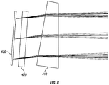
- the turning prism 324 directs the optical beams to the compensating prism 410, window 420 and DMD 430 in FIG. 8 . Additional details concerning the wavelength blocker array is described below in connection with FIG. 11 .
- the launch optics arrangement described above may also be used as a simple switch by placing one or more mirrors at the virtual focal point, with up to one mirror for each coupling lens pair.
- the mirrors may be provided in the form of a DMD. By actuating the individual mirrors the optical communication path between the input and output can be switched on and off. Additional details concerning the use of this arrangement as a fiber array switch device is presented below in connection with FIG. 9 .
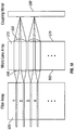
- FIG. 9 shows an example of a fiber array switch 500 which employs a micro lens array coupling element 510 (referred to above as an asymmetric lenslet array).
- the device consists of a fiber array 520, a double sided micro lens array 510, and a MEMs mirror array 530.
- the fiber array 520 is typically constructed by sandwiching fibers between two V-groove blocks. The fibers are spaced at a regular pitch. Common pitches are 125 or 250 um.
- the micro lens array in this design is a double sided array.
- the coupling lenses 540 are equally spaced and have the same pitch as the fibers in the fiber array 520.
- the side facing the MEMS mirrors consists of a linear array of combining lenses 550.
- the pitch of the combining lenses 550 is double the pitch of the fibers in the fiber array.
- the final element is the linear array of MEMS mirrors 530.
- the function of the switch 500 is to couple the light from one fiber to its neighbor.
- Light exiting fiber 1 is collimated by the coupling lens 540 on side 560 of the micro lens array 510.
- This beam passes thru the micro lens array 510 and is focused by the combining lens 550 on side 570 onto one of the MEMS mirrors in the MEMs mirror array 530.
- the MEMS mirror is oriented normally, the beam will reflect off the MEMs mirrors back into the combining lens 550 where it will be recollimated and pass thru the micro lens array onto the neighboring coupling lens.
- This coupling lens then focuses the beam back onto fiber 2. In this way all of the fibers in the array are coupled in pairs.
- the MEMS mirror is tilted away from the normal, the beam is dumped and no connection is made.
- An array of 1 x 2 switches could be made with a micro lens array where the combiner couples 3 neighboring fibers.
- FIG. 3b shows a two component assembly where the micro lens array (referred to above as an asymmetric lenslet array) is bonded to a mounting surface on the fiber array.
- Proper functioning of the fiber array-micro lens array assembly depends on accurate alignment of the two components.
- FIG. 10 shows a method for aligning the micro lens array 510 to the fiber array 520 using a coupling mirror 580 located at the virtual image plane. When properly aligned, this configuration will efficiently couple the fibers in pairs across the entire fiber array 520. Light injected into fiber 1 will be efficiently coupled out of fiber 2 and so on across the array. To align the assembly, one simple monitors the coupling across the array while adjusting the alignment of the micro lens array 510 to the fiber array 520. When good coupling is achieved across the fiber array 520, the micro lens array 510 is bonded to the fiber array.
- FIGs. 11a and 11b show a top view and side view, respectively, of one example of a 1XN wave blocker array which employs a fiber array-micro lens array launch optical arrangement as described above.
- the design consists of a linear fiber array (FA) followed by a double sided, micro lens array (ML) (i.e, the asymmetric lenslet assembly discussed above).
- the fiber array consists of 2N fibers sandwiched between V-groove plates. The exit face of the V-groove plate is often polished at an angle to prevent back reflections.
- the fibers in the array are equally spaced.
- Typical fiber spacing (pitch) is 125 or 250 microns.
- the micro lens array has a linear array of lenses on each side.
- the side facing the fiber array has 2N collimating lens, one for each fiber. These lenses are equally spaced having the same pitch as the fiber array.
- the side facing the DMD has a linear array of N coupling lenses having a pitch of twice the fiber pitch.
- This double sided micro lens array is designed to couple the light from adjacent fibers by overlapping their images at the launch plane (LP).
- the micro lens array is followed by a collimating lens (CL), a diffraction grating (G), a scan lens (SL), a compensating prism (P), and finally a MEMS micro mirror array here referred to as "DMD.”
- the rays in the top view show the wavelength filtering operation of the device.
- Light exiting the fiber under consideration is collimated by a collimating lens on the front side of the microlens array.
- the collimated beam passes thru the micro lens array and is then focused by a coupling lens onto the "launch plane".
- the collimating lens recollimates this beam.
- the grating (G) then diffracts the collimated beam according to the grating equation.
- the scan lens (SL) focuses the spectrally dispersed beams onto the DMD mirror surface. If the DMD is set to pass a given wavelength, this beam will reflect off the DMD mirror and travel back thru the system to the neighboring exit fiber.
- the side view shown in Figure 11b shows how this coupling is achieved.
- This view shows the chief ray from the coupled pair of fibers.
- the ray exiting fiber "A" passes thru the system and focuses down onto the DMD. Because the DMD is tilted, this beam will reflect out of the system (dashed beam) unless the DMD mirrors are switch to the couple state. In the coupled state, the DMD mirrors are tilted up to reflect the beam nearly back onto itself (i.e. near Littrow condition). This beam then travels back thru the system to the micro lens array. However, due to the slight angular separation generated at the DMD, the coupling lens relays the beam to the neighboring collimating lens which focuses the beam on the neighboring fiber "B" and exits the system on this fiber.
- the side view shows the operation of only one coupled fiber pair (port), the coupling described above occurs for all of the fiber pairs. Note, however, that because the DMD is tilted, the distance from the scan lens to the DMD varies from port to port. The function of the compensating prism (P) is to exactly correct this path length difference so that all ports come to a focus on the DMD.
Landscapes
- Physics & Mathematics (AREA)
- General Physics & Mathematics (AREA)
- Optics & Photonics (AREA)
- Optical Couplings Of Light Guides (AREA)
- Mechanical Light Control Or Optical Switches (AREA)
Claims (10)
- Optische Einkopplungsanordnung, umfassend:eine Faserbaugruppe zum Halten einer Matrixanordnung von optischen Fasern (105); undeine asymmetrische Linsenmatrixanordnung (200), die eine erste Fläche (220) mit einer Vielzahl von Paaren (2101, 2102, 2103, 2104) von Kopplungslinsen (212), wobei jede von den Kopplungslinsen (212) in Ausrichtung mit einer optischen Faser (105) in der Matrixanordnung von optischen Fasern (105) ist, und eine zweite Fläche (230) mit einer Vielzahl von Kollimationslinsen (2141, 2142, 2143, 2144) aufweist, wobei jede von den Kollimationslinsen (2141, 2142, 2143, 2144) in Ausrichtung mit einem von den Paaren (2101, 2102, 2103, 2104) von Kopplungslinsen (212) ist.
- Optische Einkopplungsanordnung nach Anspruch 1, wobei die Faserbaugruppe eine V-Nut-Baugruppe (250) zum Halten der optischen Fasern (105) und eine Wellenleitereinheit (100B) umfasst, die einen Wellenleiter für jede optische Faser (105) in der Matrixanordnung von optischen Fasern aufweist, wobei jede V-Nut in der V-Nut-Baugruppe (250) mit einem Kern (103) von einem der Wellenleiter in der Wellenleitereinheit (100B) ausgerichtet ist.
- Optische Einkopplungsanordnung nach Anspruch 2, wobei ein Pitch der Wellenleiter gleich einem Pitch der Kopplungslinsen (212) ist.
- Optische Einkopplungsanordnung nach Anspruch 1, die überdies ein Substrat (280) umfasst, auf dem die Faserbaugruppe und die asymmetrische Linsenmatrixanordnung (200) montiert sind.
- Optische Einkopplungsanordnung nach Anspruch 4, wobei die zweite Fläche (230) der asymmetrischen Linsenmatrixanordnung (200) winklig von einer Ausgangsfläche der Wellenleitereinheit (100B) versetzt ist.
- Optische Einkopplungsanordnung nach Anspruch 5, die überdies eine Antireflexbeschichtung umfasst, die auf mindestens einer von der ersten und der zweiten Fläche (220, 230) der asymmetrischen Linsenmatrixanordnung (200) gebildet ist.
- Optische Einkopplungsanordnung nach Anspruch 1, wobei ein Abstand zwischen jeder Kollimationslinse (2141, 2142, 2143, 2144) und den Kopplungslinsen (212), die damit in Ausrichtung sind, etwa gleich einer Summe einer Brennweite der entsprechenden Kollimationslinse (2141, 2142, 2143, 2144) und einer Brennweite von einer von den Kopplungslinsen (212) ist.
- Optische Einkopplungsanordnung nach Anspruch 1, die überdies eine optisch transparente Baugruppe umfasst, auf der die erste und die zweite Fläche (220, 230) der asymmetrischen Linsenmatrixanordnung (200) sich befinden.
- Optische Einkopplungsanordnung nach Anspruch 1, wobei die Kopplungslinsen (212) in jedem Paar ausgestaltet sind, um gleich zu sein.
- Optische Einkopplungsanordnung nach Anspruch 1, wobei die Kopplungslinsen (212) unterschiedliche Ausgestaltungen aufweisen.
Priority Applications (1)
| Application Number | Priority Date | Filing Date | Title |
|---|---|---|---|
| EP18157581.2A EP3399358B1 (de) | 2011-08-24 | 2012-08-23 | Asymmetrisches linsenarray |
Applications Claiming Priority (1)
| Application Number | Priority Date | Filing Date | Title |
|---|---|---|---|
| US201161526791P | 2011-08-24 | 2011-08-24 |
Related Child Applications (1)
| Application Number | Title | Priority Date | Filing Date |
|---|---|---|---|
| EP18157581.2A Division EP3399358B1 (de) | 2011-08-24 | 2012-08-23 | Asymmetrisches linsenarray |
Publications (2)
| Publication Number | Publication Date |
|---|---|
| EP2562574A1 EP2562574A1 (de) | 2013-02-27 |
| EP2562574B1 true EP2562574B1 (de) | 2018-02-21 |
Family
ID=47215308
Family Applications (2)
| Application Number | Title | Priority Date | Filing Date |
|---|---|---|---|
| EP18157581.2A Active EP3399358B1 (de) | 2011-08-24 | 2012-08-23 | Asymmetrisches linsenarray |
| EP12006027.2A Active EP2562574B1 (de) | 2011-08-24 | 2012-08-23 | Asymmetrische Linsenmatrixanordnung |
Family Applications Before (1)
| Application Number | Title | Priority Date | Filing Date |
|---|---|---|---|
| EP18157581.2A Active EP3399358B1 (de) | 2011-08-24 | 2012-08-23 | Asymmetrisches linsenarray |
Country Status (8)
| Country | Link |
|---|---|
| US (1) | US9091817B2 (de) |
| EP (2) | EP3399358B1 (de) |
| JP (1) | JP6376319B2 (de) |
| KR (1) | KR101949530B1 (de) |
| CN (1) | CN103308986B (de) |
| AU (1) | AU2012216378B2 (de) |
| BR (1) | BR102012021436A2 (de) |
| CA (1) | CA2787565A1 (de) |
Families Citing this family (19)
| Publication number | Priority date | Publication date | Assignee | Title |
|---|---|---|---|---|
| WO2014050145A1 (ja) * | 2012-09-27 | 2014-04-03 | 日本電信電話株式会社 | 光信号処理装置 |
| US10838155B2 (en) | 2013-06-14 | 2020-11-17 | Chiral Photonics, Inc. | Multichannel optical coupler |
| US10914891B2 (en) * | 2013-06-14 | 2021-02-09 | Chiral Photonics, Inc. | Multichannel optical coupler |
| US11156781B2 (en) * | 2013-06-14 | 2021-10-26 | Chiral Photonics, Inc. | Passive aligning optical coupler array |
| US11966091B2 (en) * | 2013-06-14 | 2024-04-23 | Chiral Photonics, Inc. | Multichannel optical coupler array |
| US10564348B2 (en) * | 2013-06-14 | 2020-02-18 | Chiral Photonics, Inc. | Passive aligning optical coupler array |
| US9008514B2 (en) | 2013-06-22 | 2015-04-14 | Mark E. Boduch | Method and apparatus for construction of compact optical nodes using wavelength equalizing arrays |
| US10135560B2 (en) | 2013-06-22 | 2018-11-20 | Mark E. Boduch | Optical devices for the construction of compact optical nodes |
| US10389470B2 (en) | 2013-06-22 | 2019-08-20 | Mark E. Boduch | Construction of optical nodes using programmable ROADMS |
| CN103969770B (zh) * | 2014-04-03 | 2016-03-09 | 深圳日海通讯技术股份有限公司 | 一种光纤连接器 |
| JP2016218406A (ja) * | 2015-05-26 | 2016-12-22 | 富士通オプティカルコンポーネンツ株式会社 | 光変調器モジュール |
| US9423561B1 (en) * | 2015-06-19 | 2016-08-23 | Inphi Corporation | Method of attaching fiber block to silicon photonics |
| US9921408B2 (en) | 2016-02-26 | 2018-03-20 | Qualcomm Incorporated | Collimating light emitted by a fiber via an array of lenslets on a curved surface |
| US10042121B1 (en) * | 2017-03-28 | 2018-08-07 | Nistica, Inc. | Toroidal micro lens array for use in a wavelength selective switch |
| CN108089263A (zh) * | 2017-12-29 | 2018-05-29 | 山东明灿光电科技有限公司 | 一种多模-单模混合型光分路器及其制作方法 |
| CN112955784B (zh) * | 2018-09-14 | 2024-12-31 | 纽约市哥伦比亚大学理事会 | 基于光学开关阵列的光束方向控制与接收方法 |
| US11444695B2 (en) * | 2019-09-13 | 2022-09-13 | Fathom Radiant, PBC | Optical shuffle computation network |
| US12210185B2 (en) | 2020-02-24 | 2025-01-28 | Chiral Photonics, Inc. | Wavelength division multiplexers for space division multiplexing (SDM-WDM devices) |
| US11446776B2 (en) * | 2020-08-27 | 2022-09-20 | Northrop Grumman Systems Corporation | Method for assembling a hollow core optical fiber array launcher |
Citations (2)
| Publication number | Priority date | Publication date | Assignee | Title |
|---|---|---|---|---|
| US5319496A (en) * | 1992-11-18 | 1994-06-07 | Photonics Research Incorporated | Optical beam delivery system |
| US20020001140A1 (en) * | 1999-11-23 | 2002-01-03 | Radiant Optics, Inc. | Collecting and organizing means for multiple light sources |
Family Cites Families (44)
| Publication number | Priority date | Publication date | Assignee | Title |
|---|---|---|---|---|
| JPS6424209A (en) * | 1987-07-21 | 1989-01-26 | Hoya Corp | Optical distributor/coupler |
| US5412506A (en) * | 1992-03-09 | 1995-05-02 | At&T Corp. | Free-space optical interconnection arrangement |
| US5742720A (en) * | 1995-08-30 | 1998-04-21 | Matsushita Electric Industrial Co., Ltd. | Optical coupling module and method for producing the same |
| FR2754354B1 (fr) * | 1996-10-08 | 1998-11-06 | France Telecom | Dispositif de connexion pour fibre optique multicoeur, a base d'elements optiques en espace libre |
| JPH10142458A (ja) * | 1996-11-08 | 1998-05-29 | Mitsubishi Cable Ind Ltd | 光ファイバアレイ |
| JPH1183459A (ja) * | 1997-09-01 | 1999-03-26 | Fujitsu Ltd | 凹凸面情報検出装置 |
| US6339503B1 (en) * | 1998-11-06 | 2002-01-15 | Oni Systems Corp. | Optical interconnect using microlens/minilens relay |
| JP2001242339A (ja) * | 2000-03-01 | 2001-09-07 | Nippon Sheet Glass Co Ltd | 光ファイバーレンズアレイ |
| JP2002006397A (ja) * | 2000-06-22 | 2002-01-09 | Sony Corp | 画像表示装置 |
| JP2002072157A (ja) * | 2000-08-24 | 2002-03-12 | Nippon Telegr & Teleph Corp <Ntt> | 波長可変フィルター及び空間光スイッチ |
| US6430328B1 (en) | 2000-10-13 | 2002-08-06 | William H. Culver | Optical switch |
| US20030002789A1 (en) * | 2000-10-31 | 2003-01-02 | Boye Robert R. | Integrated optical coupler |
| CA2327862A1 (en) * | 2000-11-20 | 2002-05-20 | Thomas Ducellier | Optical switch |
| US6625350B2 (en) * | 2001-01-22 | 2003-09-23 | Osaki Electric Co., Ltd. | Fiber collimator array |
| US6956687B2 (en) | 2001-04-03 | 2005-10-18 | Cidra Corporation | Optical blocking filter having an array of micro-mirrors |
| US7123833B2 (en) | 2001-08-09 | 2006-10-17 | Cidra Corporation | Dynamically reconfigurable optical smart node |
| US7126740B2 (en) | 2001-04-03 | 2006-10-24 | Cidra Corporation | Multifunctional optical device having a spatial light modulator with an array of micromirrors |
| JP2002365508A (ja) * | 2001-06-08 | 2002-12-18 | Nippon Sheet Glass Co Ltd | 光モジュールのアライメント方法、光モジュール、光モジュールのアライメント装置 |
| US6657770B2 (en) * | 2001-06-22 | 2003-12-02 | Lucent Technologies Inc. | Programmable optical multiplexer/demultiplexer |
| US6757458B2 (en) * | 2001-06-29 | 2004-06-29 | Lucent Technologies Inc. | Optical MEMS switch with converging beams |
| US6707959B2 (en) * | 2001-07-12 | 2004-03-16 | Jds Uniphase Inc. | Wavelength switch |
| JP2003043295A (ja) * | 2001-07-31 | 2003-02-13 | Nippon Sheet Glass Co Ltd | 光モジュールユニットおよびこのユニットを用いた光モジュール |
| JP2003241005A (ja) * | 2002-02-14 | 2003-08-27 | Nippon Sheet Glass Co Ltd | 光モジュール |
| US20060165351A1 (en) * | 2002-06-14 | 2006-07-27 | Nippon Sheet Glass Co., Ltd. | Optical device unit, optical device and microlens array |
| US20030231829A1 (en) * | 2002-06-18 | 2003-12-18 | Meyers Mark M. | Lens array for use with array of fibers |
| US7004645B2 (en) * | 2003-04-30 | 2006-02-28 | Agilent Technologies, Inc. | VCSEL array configuration for a parallel WDM transmitter |
| JP4347224B2 (ja) * | 2003-05-15 | 2009-10-21 | 富士通株式会社 | 光デバイス |
| US7162115B2 (en) * | 2003-05-31 | 2007-01-09 | Jds Uniphase Corporation | Multiport wavelength-selective optical switch |
| US6768834B1 (en) * | 2003-06-13 | 2004-07-27 | Agilent Technologies, Inc. | Slab optical multiplexer |
| JP2005070073A (ja) * | 2003-08-21 | 2005-03-17 | Nippon Sheet Glass Co Ltd | 光ファイバコリメータ |
| US7092599B2 (en) | 2003-11-12 | 2006-08-15 | Engana Pty Ltd | Wavelength manipulation system and method |
| US7653278B2 (en) * | 2004-05-21 | 2010-01-26 | Panasonic Corporation | Refractive index distribution type optical member, and production method for refractive index distribution type optical member |
| US7397980B2 (en) | 2004-06-14 | 2008-07-08 | Optium Australia Pty Limited | Dual-source optical wavelength processor |
| CN100565274C (zh) * | 2004-06-23 | 2009-12-02 | 株式会社尼康 | 光学元件、光学系统及波导 |
| JP4476140B2 (ja) * | 2005-03-07 | 2010-06-09 | 富士通株式会社 | 波長選択スイッチ |
| US7231106B2 (en) * | 2005-09-30 | 2007-06-12 | Lucent Technologies Inc. | Apparatus for directing an optical signal from an input fiber to an output fiber within a high index host |
| JP2007114454A (ja) * | 2005-10-20 | 2007-05-10 | Yamaha Corp | マイクロレンズアレイとその製法 |
| JP2007248731A (ja) * | 2006-03-15 | 2007-09-27 | Hitachi Metals Ltd | マイクロミラー並びにそれを用いた光部品および光スイッチ |
| US7556440B2 (en) * | 2006-12-22 | 2009-07-07 | Lightwire Inc. | Dual-lensed unitary optical receiver assembly |
| JP2010160218A (ja) * | 2009-01-06 | 2010-07-22 | Mitsubishi Electric Corp | 受光装置および光送受信装置 |
| JP5012855B2 (ja) * | 2009-06-10 | 2012-08-29 | 富士通株式会社 | 光デバイス |
| CN102096148A (zh) * | 2010-11-19 | 2011-06-15 | 四川天邑康和光电子有限公司 | 光纤阵列及其制造方法 |
| US9229169B2 (en) * | 2011-08-16 | 2016-01-05 | International Business Machines Corporation | Lens array optical coupling to photonic chip |
| US20130064507A1 (en) * | 2011-09-09 | 2013-03-14 | Sven Mahnkopf | Wavelength division multiplexing device |
-
2012
- 2012-08-22 AU AU2012216378A patent/AU2012216378B2/en not_active Ceased
- 2012-08-22 JP JP2012183582A patent/JP6376319B2/ja active Active
- 2012-08-22 CA CA2787565A patent/CA2787565A1/en not_active Abandoned
- 2012-08-23 EP EP18157581.2A patent/EP3399358B1/de active Active
- 2012-08-23 EP EP12006027.2A patent/EP2562574B1/de active Active
- 2012-08-23 KR KR1020120092231A patent/KR101949530B1/ko active Active
- 2012-08-24 CN CN201210304323.0A patent/CN103308986B/zh active Active
- 2012-08-24 US US13/593,870 patent/US9091817B2/en active Active
- 2012-08-24 BR BR102012021436-9A patent/BR102012021436A2/pt not_active Application Discontinuation
Patent Citations (2)
| Publication number | Priority date | Publication date | Assignee | Title |
|---|---|---|---|---|
| US5319496A (en) * | 1992-11-18 | 1994-06-07 | Photonics Research Incorporated | Optical beam delivery system |
| US20020001140A1 (en) * | 1999-11-23 | 2002-01-03 | Radiant Optics, Inc. | Collecting and organizing means for multiple light sources |
Also Published As
| Publication number | Publication date |
|---|---|
| KR20130022382A (ko) | 2013-03-06 |
| CN103308986A (zh) | 2013-09-18 |
| BR102012021436A2 (pt) | 2013-12-03 |
| EP3399358B1 (de) | 2024-06-19 |
| AU2012216378B2 (en) | 2015-09-17 |
| US20130051726A1 (en) | 2013-02-28 |
| EP2562574A1 (de) | 2013-02-27 |
| CN103308986B (zh) | 2017-05-03 |
| AU2012216378A1 (en) | 2013-03-14 |
| JP2013045114A (ja) | 2013-03-04 |
| EP3399358A1 (de) | 2018-11-07 |
| JP6376319B2 (ja) | 2018-08-22 |
| KR101949530B1 (ko) | 2019-02-18 |
| CA2787565A1 (en) | 2013-02-24 |
| US9091817B2 (en) | 2015-07-28 |
Similar Documents
| Publication | Publication Date | Title |
|---|---|---|
| EP3399358B1 (de) | Asymmetrisches linsenarray | |
| US8731403B2 (en) | Multicast optical switch | |
| US7889991B2 (en) | Planar lightwave circuit based tunable 3 port filter | |
| US7164859B2 (en) | Free-space dynamic wavelength routing systems with interleaved channels for enhanced performance | |
| US7599587B2 (en) | Wavelength selective switch | |
| US6978061B1 (en) | Optical switching device | |
| US20160197695A1 (en) | Optical Signal Processing Device | |
| KR101958395B1 (ko) | 디지털 마이크로미러 디바이스를 이용하고 감소된 파장 의존 손실을 가지는 광학적 프로세싱 디바이스 | |
| US20040136074A1 (en) | Tunable spectral filter | |
| US20130177272A1 (en) | Systems And Methods For Reducing Off-Axis Optical Aberrations In Wavelength Dispersed Devices | |
| EP2083298B1 (de) | Optische Vorrichtung mit einem kompakten Dispersionssystem | |
| US20060159395A1 (en) | Optical compensator array for dispersive element arrays | |
| US7277607B2 (en) | Optical multiplexer/demultiplexer, optical device, and optical transmission system | |
| KR101832874B1 (ko) | 광 교차연결 장치 | |
| JP2012173720A (ja) | 波長選択スイッチ | |
| CA2538965A1 (en) | Wavelength compensated optical wavelength division coupler and associated methods |
Legal Events
| Date | Code | Title | Description |
|---|---|---|---|
| PUAI | Public reference made under article 153(3) epc to a published international application that has entered the european phase |
Free format text: ORIGINAL CODE: 0009012 |
|
| AK | Designated contracting states |
Kind code of ref document: A1 Designated state(s): AL AT BE BG CH CY CZ DE DK EE ES FI FR GB GR HR HU IE IS IT LI LT LU LV MC MK MT NL NO PL PT RO RS SE SI SK SM TR |
|
| AX | Request for extension of the european patent |
Extension state: BA ME |
|
| 17P | Request for examination filed |
Effective date: 20130814 |
|
| RBV | Designated contracting states (corrected) |
Designated state(s): AL AT BE BG CH CY CZ DE DK EE ES FI FR GB GR HR HU IE IS IT LI LT LU LV MC MK MT NL NO PL PT RO RS SE SI SK SM TR |
|
| STAA | Information on the status of an ep patent application or granted ep patent |
Free format text: STATUS: EXAMINATION IS IN PROGRESS |
|
| 17Q | First examination report despatched |
Effective date: 20161121 |
|
| GRAP | Despatch of communication of intention to grant a patent |
Free format text: ORIGINAL CODE: EPIDOSNIGR1 |
|
| STAA | Information on the status of an ep patent application or granted ep patent |
Free format text: STATUS: GRANT OF PATENT IS INTENDED |
|
| INTG | Intention to grant announced |
Effective date: 20171009 |
|
| GRAS | Grant fee paid |
Free format text: ORIGINAL CODE: EPIDOSNIGR3 |
|
| GRAA | (expected) grant |
Free format text: ORIGINAL CODE: 0009210 |
|
| STAA | Information on the status of an ep patent application or granted ep patent |
Free format text: STATUS: THE PATENT HAS BEEN GRANTED |
|
| AK | Designated contracting states |
Kind code of ref document: B1 Designated state(s): AL AT BE BG CH CY CZ DE DK EE ES FI FR GB GR HR HU IE IS IT LI LT LU LV MC MK MT NL NO PL PT RO RS SE SI SK SM TR |
|
| REG | Reference to a national code |
Ref country code: GB Ref legal event code: FG4D |
|
| REG | Reference to a national code |
Ref country code: CH Ref legal event code: EP |
|
| REG | Reference to a national code |
Ref country code: AT Ref legal event code: REF Ref document number: 972349 Country of ref document: AT Kind code of ref document: T Effective date: 20180315 |
|
| REG | Reference to a national code |
Ref country code: IE Ref legal event code: FG4D |
|
| REG | Reference to a national code |
Ref country code: DE Ref legal event code: R096 Ref document number: 602012042923 Country of ref document: DE |
|
| REG | Reference to a national code |
Ref country code: NL Ref legal event code: MP Effective date: 20180221 |
|
| REG | Reference to a national code |
Ref country code: LT Ref legal event code: MG4D |
|
| REG | Reference to a national code |
Ref country code: AT Ref legal event code: MK05 Ref document number: 972349 Country of ref document: AT Kind code of ref document: T Effective date: 20180221 |
|
| PG25 | Lapsed in a contracting state [announced via postgrant information from national office to epo] |
Ref country code: HR Free format text: LAPSE BECAUSE OF FAILURE TO SUBMIT A TRANSLATION OF THE DESCRIPTION OR TO PAY THE FEE WITHIN THE PRESCRIBED TIME-LIMIT Effective date: 20180221 Ref country code: FI Free format text: LAPSE BECAUSE OF FAILURE TO SUBMIT A TRANSLATION OF THE DESCRIPTION OR TO PAY THE FEE WITHIN THE PRESCRIBED TIME-LIMIT Effective date: 20180221 Ref country code: NO Free format text: LAPSE BECAUSE OF FAILURE TO SUBMIT A TRANSLATION OF THE DESCRIPTION OR TO PAY THE FEE WITHIN THE PRESCRIBED TIME-LIMIT Effective date: 20180521 Ref country code: LT Free format text: LAPSE BECAUSE OF FAILURE TO SUBMIT A TRANSLATION OF THE DESCRIPTION OR TO PAY THE FEE WITHIN THE PRESCRIBED TIME-LIMIT Effective date: 20180221 Ref country code: CY Free format text: LAPSE BECAUSE OF FAILURE TO SUBMIT A TRANSLATION OF THE DESCRIPTION OR TO PAY THE FEE WITHIN THE PRESCRIBED TIME-LIMIT Effective date: 20180221 Ref country code: NL Free format text: LAPSE BECAUSE OF FAILURE TO SUBMIT A TRANSLATION OF THE DESCRIPTION OR TO PAY THE FEE WITHIN THE PRESCRIBED TIME-LIMIT Effective date: 20180221 Ref country code: ES Free format text: LAPSE BECAUSE OF FAILURE TO SUBMIT A TRANSLATION OF THE DESCRIPTION OR TO PAY THE FEE WITHIN THE PRESCRIBED TIME-LIMIT Effective date: 20180221 |
|
| REG | Reference to a national code |
Ref country code: FR Ref legal event code: PLFP Year of fee payment: 7 |
|
| PG25 | Lapsed in a contracting state [announced via postgrant information from national office to epo] |
Ref country code: AT Free format text: LAPSE BECAUSE OF FAILURE TO SUBMIT A TRANSLATION OF THE DESCRIPTION OR TO PAY THE FEE WITHIN THE PRESCRIBED TIME-LIMIT Effective date: 20180221 Ref country code: RS Free format text: LAPSE BECAUSE OF FAILURE TO SUBMIT A TRANSLATION OF THE DESCRIPTION OR TO PAY THE FEE WITHIN THE PRESCRIBED TIME-LIMIT Effective date: 20180221 Ref country code: SE Free format text: LAPSE BECAUSE OF FAILURE TO SUBMIT A TRANSLATION OF THE DESCRIPTION OR TO PAY THE FEE WITHIN THE PRESCRIBED TIME-LIMIT Effective date: 20180221 Ref country code: LV Free format text: LAPSE BECAUSE OF FAILURE TO SUBMIT A TRANSLATION OF THE DESCRIPTION OR TO PAY THE FEE WITHIN THE PRESCRIBED TIME-LIMIT Effective date: 20180221 Ref country code: GR Free format text: LAPSE BECAUSE OF FAILURE TO SUBMIT A TRANSLATION OF THE DESCRIPTION OR TO PAY THE FEE WITHIN THE PRESCRIBED TIME-LIMIT Effective date: 20180522 Ref country code: BG Free format text: LAPSE BECAUSE OF FAILURE TO SUBMIT A TRANSLATION OF THE DESCRIPTION OR TO PAY THE FEE WITHIN THE PRESCRIBED TIME-LIMIT Effective date: 20180521 |
|
| PG25 | Lapsed in a contracting state [announced via postgrant information from national office to epo] |
Ref country code: RO Free format text: LAPSE BECAUSE OF FAILURE TO SUBMIT A TRANSLATION OF THE DESCRIPTION OR TO PAY THE FEE WITHIN THE PRESCRIBED TIME-LIMIT Effective date: 20180221 Ref country code: EE Free format text: LAPSE BECAUSE OF FAILURE TO SUBMIT A TRANSLATION OF THE DESCRIPTION OR TO PAY THE FEE WITHIN THE PRESCRIBED TIME-LIMIT Effective date: 20180221 Ref country code: PL Free format text: LAPSE BECAUSE OF FAILURE TO SUBMIT A TRANSLATION OF THE DESCRIPTION OR TO PAY THE FEE WITHIN THE PRESCRIBED TIME-LIMIT Effective date: 20180221 Ref country code: AL Free format text: LAPSE BECAUSE OF FAILURE TO SUBMIT A TRANSLATION OF THE DESCRIPTION OR TO PAY THE FEE WITHIN THE PRESCRIBED TIME-LIMIT Effective date: 20180221 |
|
| PGFP | Annual fee paid to national office [announced via postgrant information from national office to epo] |
Ref country code: CH Payment date: 20170912 Year of fee payment: 16 |
|
| REG | Reference to a national code |
Ref country code: DE Ref legal event code: R097 Ref document number: 602012042923 Country of ref document: DE |
|
| PG25 | Lapsed in a contracting state [announced via postgrant information from national office to epo] |
Ref country code: SM Free format text: LAPSE BECAUSE OF FAILURE TO SUBMIT A TRANSLATION OF THE DESCRIPTION OR TO PAY THE FEE WITHIN THE PRESCRIBED TIME-LIMIT Effective date: 20180221 Ref country code: DK Free format text: LAPSE BECAUSE OF FAILURE TO SUBMIT A TRANSLATION OF THE DESCRIPTION OR TO PAY THE FEE WITHIN THE PRESCRIBED TIME-LIMIT Effective date: 20180221 Ref country code: SK Free format text: LAPSE BECAUSE OF FAILURE TO SUBMIT A TRANSLATION OF THE DESCRIPTION OR TO PAY THE FEE WITHIN THE PRESCRIBED TIME-LIMIT Effective date: 20180221 Ref country code: CZ Free format text: LAPSE BECAUSE OF FAILURE TO SUBMIT A TRANSLATION OF THE DESCRIPTION OR TO PAY THE FEE WITHIN THE PRESCRIBED TIME-LIMIT Effective date: 20180221 |
|
| PLBE | No opposition filed within time limit |
Free format text: ORIGINAL CODE: 0009261 |
|
| STAA | Information on the status of an ep patent application or granted ep patent |
Free format text: STATUS: NO OPPOSITION FILED WITHIN TIME LIMIT |
|
| 26N | No opposition filed |
Effective date: 20181122 |
|
| PG25 | Lapsed in a contracting state [announced via postgrant information from national office to epo] |
Ref country code: SI Free format text: LAPSE BECAUSE OF FAILURE TO SUBMIT A TRANSLATION OF THE DESCRIPTION OR TO PAY THE FEE WITHIN THE PRESCRIBED TIME-LIMIT Effective date: 20180221 |
|
| PGFP | Annual fee paid to national office [announced via postgrant information from national office to epo] |
Ref country code: FR Payment date: 20181127 Year of fee payment: 8 |
|
| PG25 | Lapsed in a contracting state [announced via postgrant information from national office to epo] |
Ref country code: MC Free format text: LAPSE BECAUSE OF FAILURE TO SUBMIT A TRANSLATION OF THE DESCRIPTION OR TO PAY THE FEE WITHIN THE PRESCRIBED TIME-LIMIT Effective date: 20180221 |
|
| REG | Reference to a national code |
Ref country code: CH Ref legal event code: PL |
|
| PG25 | Lapsed in a contracting state [announced via postgrant information from national office to epo] |
Ref country code: LU Free format text: LAPSE BECAUSE OF NON-PAYMENT OF DUE FEES Effective date: 20180823 Ref country code: CH Free format text: LAPSE BECAUSE OF NON-PAYMENT OF DUE FEES Effective date: 20180831 Ref country code: LI Free format text: LAPSE BECAUSE OF NON-PAYMENT OF DUE FEES Effective date: 20180831 |
|
| REG | Reference to a national code |
Ref country code: BE Ref legal event code: MM Effective date: 20180831 |
|
| PG25 | Lapsed in a contracting state [announced via postgrant information from national office to epo] |
Ref country code: BE Free format text: LAPSE BECAUSE OF NON-PAYMENT OF DUE FEES Effective date: 20180831 |
|
| PG25 | Lapsed in a contracting state [announced via postgrant information from national office to epo] |
Ref country code: MT Free format text: LAPSE BECAUSE OF NON-PAYMENT OF DUE FEES Effective date: 20180823 |
|
| PG25 | Lapsed in a contracting state [announced via postgrant information from national office to epo] |
Ref country code: TR Free format text: LAPSE BECAUSE OF FAILURE TO SUBMIT A TRANSLATION OF THE DESCRIPTION OR TO PAY THE FEE WITHIN THE PRESCRIBED TIME-LIMIT Effective date: 20180221 |
|
| PG25 | Lapsed in a contracting state [announced via postgrant information from national office to epo] |
Ref country code: HU Free format text: LAPSE BECAUSE OF FAILURE TO SUBMIT A TRANSLATION OF THE DESCRIPTION OR TO PAY THE FEE WITHIN THE PRESCRIBED TIME-LIMIT; INVALID AB INITIO Effective date: 20120823 Ref country code: PT Free format text: LAPSE BECAUSE OF FAILURE TO SUBMIT A TRANSLATION OF THE DESCRIPTION OR TO PAY THE FEE WITHIN THE PRESCRIBED TIME-LIMIT Effective date: 20180221 |
|
| PG25 | Lapsed in a contracting state [announced via postgrant information from national office to epo] |
Ref country code: IE Free format text: LAPSE BECAUSE OF NON-PAYMENT OF DUE FEES Effective date: 20180823 Ref country code: MK Free format text: LAPSE BECAUSE OF NON-PAYMENT OF DUE FEES Effective date: 20180221 |
|
| PG25 | Lapsed in a contracting state [announced via postgrant information from national office to epo] |
Ref country code: IS Free format text: LAPSE BECAUSE OF FAILURE TO SUBMIT A TRANSLATION OF THE DESCRIPTION OR TO PAY THE FEE WITHIN THE PRESCRIBED TIME-LIMIT Effective date: 20180621 |
|
| PG25 | Lapsed in a contracting state [announced via postgrant information from national office to epo] |
Ref country code: IT Free format text: LAPSE BECAUSE OF NON-PAYMENT OF DUE FEES Effective date: 20190823 |
|
| REG | Reference to a national code |
Ref country code: GB Ref legal event code: 732E Free format text: REGISTERED BETWEEN 20201112 AND 20201118 |
|
| REG | Reference to a national code |
Ref country code: DE Ref legal event code: R082 Ref document number: 602012042923 Country of ref document: DE Representative=s name: HAUCK PATENTANWALTSPARTNERSCHAFT MBB, DE Ref country code: DE Ref legal event code: R081 Ref document number: 602012042923 Country of ref document: DE Owner name: MOLEX, LLC (N.D.GES.D.STAATES DELAWARE), WELLI, US Free format text: FORMER OWNER: NISTICA, INC., BRIDGEWATER, N.J, US |
|
| PG25 | Lapsed in a contracting state [announced via postgrant information from national office to epo] |
Ref country code: FR Free format text: LAPSE BECAUSE OF NON-PAYMENT OF DUE FEES Effective date: 20200831 |
|
| P01 | Opt-out of the competence of the unified patent court (upc) registered |
Effective date: 20230528 |
|
| PGFP | Annual fee paid to national office [announced via postgrant information from national office to epo] |
Ref country code: DE Payment date: 20250702 Year of fee payment: 14 |
|
| PGFP | Annual fee paid to national office [announced via postgrant information from national office to epo] |
Ref country code: GB Payment date: 20250703 Year of fee payment: 14 |