EP2560462B1 - Organic electroluminescent illumination device - Google Patents
Organic electroluminescent illumination device Download PDFInfo
- Publication number
- EP2560462B1 EP2560462B1 EP11792264.1A EP11792264A EP2560462B1 EP 2560462 B1 EP2560462 B1 EP 2560462B1 EP 11792264 A EP11792264 A EP 11792264A EP 2560462 B1 EP2560462 B1 EP 2560462B1
- Authority
- EP
- European Patent Office
- Prior art keywords
- electrode films
- auxiliary electrode
- film
- relation
- films
- Prior art date
- Legal status (The legal status is an assumption and is not a legal conclusion. Google has not performed a legal analysis and makes no representation as to the accuracy of the status listed.)
- Not-in-force
Links
Images


Classifications
-
- H—ELECTRICITY
- H05—ELECTRIC TECHNIQUES NOT OTHERWISE PROVIDED FOR
- H05B—ELECTRIC HEATING; ELECTRIC LIGHT SOURCES NOT OTHERWISE PROVIDED FOR; CIRCUIT ARRANGEMENTS FOR ELECTRIC LIGHT SOURCES, IN GENERAL
- H05B33/00—Electroluminescent light sources
- H05B33/12—Light sources with substantially two-dimensional [2D] radiating surfaces
- H05B33/26—Light sources with substantially two-dimensional [2D] radiating surfaces characterised by the composition or arrangement of the conductive material used as an electrode
-
- H—ELECTRICITY
- H05—ELECTRIC TECHNIQUES NOT OTHERWISE PROVIDED FOR
- H05B—ELECTRIC HEATING; ELECTRIC LIGHT SOURCES NOT OTHERWISE PROVIDED FOR; CIRCUIT ARRANGEMENTS FOR ELECTRIC LIGHT SOURCES, IN GENERAL
- H05B33/00—Electroluminescent light sources
- H05B33/02—Details
- H05B33/06—Electrode terminals
-
- H—ELECTRICITY
- H10—SEMICONDUCTOR DEVICES; ELECTRIC SOLID-STATE DEVICES NOT OTHERWISE PROVIDED FOR
- H10K—ORGANIC ELECTRIC SOLID-STATE DEVICES
- H10K50/00—Organic light-emitting devices
- H10K50/80—Constructional details
- H10K50/805—Electrodes
- H10K50/81—Anodes
- H10K50/814—Anodes combined with auxiliary electrodes, e.g. ITO layer combined with metal lines
-
- H—ELECTRICITY
- H10—SEMICONDUCTOR DEVICES; ELECTRIC SOLID-STATE DEVICES NOT OTHERWISE PROVIDED FOR
- H10K—ORGANIC ELECTRIC SOLID-STATE DEVICES
- H10K50/00—Organic light-emitting devices
- H10K50/80—Constructional details
- H10K50/805—Electrodes
-
- H—ELECTRICITY
- H10—SEMICONDUCTOR DEVICES; ELECTRIC SOLID-STATE DEVICES NOT OTHERWISE PROVIDED FOR
- H10K—ORGANIC ELECTRIC SOLID-STATE DEVICES
- H10K50/00—Organic light-emitting devices
- H10K50/80—Constructional details
- H10K50/88—Terminals, e.g. bond pads
Definitions
- the present invention relates to an organic electroluminescent lighting device that uses, as a light source, a light-emitting element including an organic light-emitting film held between a pair of electrode films different from each other in polarity.
- One of the illumination devices is an organic electroluminescent lighting device that uses, as a light source, a light-emitting element including an organic light-emitting film held between a pair of electrode films different from each other in polarity.
- the organic light-emitting film emits light when an electric field is generated between the pair of electrode films.
- the light of the organic light-emitting film is transmitted through one of the electrode films to be applied to the outside.
- one of the electrode films is made of a transparent metallic material such as ITO (indium tin oxide), ZnO, or SnO2 (NESA glass).
- the aforementioned transparent metallic material has relatively high resistance.
- each of the opposite edge sides of its surface is a power supply terminal.
- wiring resistance increases farther away from each edge side.
- the increase of the wiring resistance is accompanied by the increase of a descending voltage. This disables uniform application of a voltage to the entire organic light-emitting film.
- the brightness of the organic light-emitting film depends on the voltage. Thus, when the voltage is not uniformly applied to the organic light-emitting film, there is a possibility that the brightness of the organic light-emitting film is not uniform.
- Patent Literature 1 JP2004-14128A ) has therefore disclosed an organic electroluminescent lighting device for preventing the occurrence of the brightness nonuniformity of the organic light-emitting film.
- the organic electroluminescent lighting device disclosed in Patent Literature 1 includes auxiliary electrodes made of materials having a lower resistance than electrode and arranged on a grid pattern in the surface of the transparent electrode. According to this organic electroluminescent lighting device, the resistance value of the entire transparent electrode is reduced by forming, in the transparent electrode, auxiliary electrodes that have a lower resistance than the transparent electrode. The wiring resistance accordingly drops to reduce the value of the descending voltage. As a result, the brightness nonuniformity of the organic light-emitting film can be prevented.
- the luminescent device includes a transparent substrate, which has a light exit surface and an incident surface, and a luminescent element, which is formed on the incident surface of the transparent substrate.
- the luminescent element includes a transparent electrode formed on the incident surface of the transparent substrate, an auxiliary electrode formed on a part of the transparent electrode, and a thin-film layer, which is formed on the transparent electrode, for emitting light.
- the transparent substrate includes a projection formed on the light exit surface.
- the luminescent device may be used for backlighting an LCD panel.
- Patent Literature 1 JP2004-14128A
- the auxiliary electrodes are similar in shape (width and film thickness) and arranged at equal intervals in the surface of the transparent electrode.
- the voltage is applied to the entire transparent electrode from each of the edge sides of the transparent electrode, voltage reduction occurs more away from the edge side (closer to the center from the edge side).
- a voltage distribution varies in the transparent electrode, causing variance on a voltage distribution in the organic light-emitting film.
- brightness uniformity is insufficient in the organic electroluminescent lighting device described in Patent Literature 1.
- an organic electroluminescent lighting device includes: an organic light-emitting film
- an organic electroluminescent lighting device comprising:
- the organic electroluminescent lighting device wherein a width of the first auxiliary electrode film becomes larger in relation to increasing distance from the edge side and a width of each of the plurality of second auxiliary electrodes films becomes larger in relation to increasing distance from the edge side.
- the plurality of first auxiliary electrode films are formed symmetrical with respect to each of a first axis and a second axis extending; wherein the first axis extends in the direction parallel to the edge side and the second axis extends in the direction perpendicular to the edge side; wherein the first axis and the second axis orthogonally intersect each other in the center of the surface of one of the electrode films; wherein a width of each of the plurality of first auxiliary electrode films becomes larger in relation to approaching the second axis; wherein the plurality of second auxiliary electrode films is formed symmetrical with respect to each of the first axis and the second axis and a width of each of the plurality of second auxiliary electrode films becomes larger in relation to approaching the second axis.
- the organic electroluminescent lighting device according to the first aspect, wherein in relation to increasing distance from the edge side a film thickness of the first auxiliary electrode film becomes thicker and a film thickness of each of the plurality of second auxiliary electrode films becomes thicker in relation to increasing distance from the edge side.
- the organic electroluminescent lighting device further comprising other power supply terminal sections which are connected to the power source; wherein the other power supply terminal sections are other edge sides which face each other at the surface of the other electrode films; and another auxiliary electrode film group including a plurality of third belt-like auxiliary electrode films and a plurality of fourth belt-like auxiliary electrode films; wherein the third auxiliary electrode films extend in a direction parallel to the other edge sides and the fourth auxiliary electrode films extend in a direction perpendicular to the edge sides; wherein the third auxiliary electrode films and the fourth auxiliary electrode films are located away from each other on the surface of the other electrode films, wherein a sectional area viewed at a section where the plurality of third auxiliary electrode films is cut in the direction perpendicular to the edge sides becomes larger in relation to increasing distance from the other edge sides and a sectional area viewed at a section where the plurality of fourth auxiliary electrode films is cut in the direction parallel to the edge sides becomes larger in relation to increasing distance from the other edge sides and a sectional area
- the sectional area of at least one of the first auxiliary electrode film and the second auxiliary electrode film becomes larger, or the wiring density of the first auxiliary electrode film becomes higher.
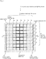
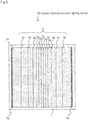
- Fig. 1 is a plan view showing the structure of organic electroluminescent lighting device 10 according to this embodiment.
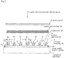
- Fig. 2 is a sectional view cut along line A1-A1 shown in Fig. 1 .
- some (interlayer insulating film 4, organic light-emitting film 5, and electrode film 2b) of the components of organic electroluminescent lighting device 10 are not shown.
- Electrode film 2a is formed on the surface of transparent substrate 1.
- Transparent substrate 1 is a glass substrate or a plastic substrate.
- Electrode film 2a is a positive electrode made of a transparent metallic material such as ITO, ZnO, or SnO2 (NESA glass). Edge sides opposite each other on the surface of electrode film 2a are power supply terminal sections 6a and 6b connected to the positive electrode of a power source.
- Auxiliary electrode film group 3 including a plurality of belt-like auxiliary electrode films 3a (first auxiliary electrode films) and a plurality of belt-like auxiliary electrode films 3b (second auxiliary electrode films) are formed on the surface of electrode film 2a.
- the plurality of auxiliary electrode films 3a are located away from each other to extend in a direction parallel to power supply terminal sections 6a and 6b (edge sides of auxiliary electrode films 3a) as shown in Fig. 1 . In relation to increasing distance from power supply terminal sections 6a and 6b, the width of auxiliary electrode films 3a becomes larger.
- the plurality of auxiliary electrode films 3b are located away from each other to extend in a direction perpendicular to power supply terminal sections 6a and 6b.
- the width of each of auxiliary electrode films 3b becomes gradually larger.
- the width of each of auxiliary electrode films 3b can become continuously larger.
- Auxiliary electrode films 3a and 3b are made of metallic materials whose resistance is lower than electrode film 2a, such as Cr (chromium), Al-Nd (aluminum-neodymium alloy), or Mo-Nb (molybdenum-niobium alloy).
- Auxiliary electrode films 3a and 3b can be two-layer films made of molybdenum and aluminum or three-layer films in which molybdenum sandwiches aluminum.
- the arrangement pattern of auxiliary electrode film group 3 is not limited to a grid pattern shown in Fig. 1 .
- auxiliary electrode film group 3 can have an arrangement pattern including only a plurality of auxiliary electrode films 3a. Further, as shown in Fig.
- auxiliary electrode film group 3 can have an arrangement pattern including only a plurality of auxiliary electrode films 3b.
- a pattern of auxiliary electrode film group 3 can be formed by taking design (symmetry) into consideration, as shown in Fig. 5 .
- the plurality of auxiliary electrode films 3a is formed to be symmetrical with respect to first axis 1 extending in the direction parallel to power supply terminal sections 6a and 6b and second axis m extending in the direction perpendicular to power supply terminal sections 6a and 6b, which orthogonally intersect each other at center C of electrode film 2a.
- auxiliary electrode films 3a In relation to approaching a second axis m, the width of auxiliary electrode films 3a becomes larger.
- Auxiliary electrode films 3b are also formed to be symmetrical with respect to first axis 1 and second axis m, and wider closer to second axis m.
- the pluralities of auxiliary electrode films 3a and 3b can be formed on the surface of electrode film 2a that is in contacted with transparent substrate 1.
- interlayer insulating film 4 (refer to Fig. 4 ) to prevent insulation degradation of organic light-emitting film 5.
- the surface of interlayer insulating film 4 is covered with organic light-emitting film 5 (refer to Fig. 2 ).
- organic light-emitting film 5 (refer to Fig. 2 ).
- the surface of organic light-emitting film 5 is covered with electrode film 2b (refer to Fig. 2 ) which pairs with electrode film 2a.
- electrode film 2b is a negative electrode made of a material whose resistance is lower than electrode film 2a, such as aluminum.
- auxiliary electrode film group 3 when a voltage is applied from the light source through power supply terminal sections 6a and 6b to entire electrode film 2a, in relation to increasing distance from power supply terminal sections 6a and 6b (in relation to approaching the center of electrode film 2a), a potential becomes lower.
- the width of auxiliary electrode films 3a in relation to increasing distance from power supply terminal sections 6a and 6b, the width of auxiliary electrode films 3a becomes larger. Accordingly, a sectional area viewed at a section where the plurality of auxiliary electrode films 3a is cut in the direction perpendicular to power supply terminal sections 6a and 6b is larger in auxiliary electrode film 3a that is separated from the power supply terminal sections 6a and 6b.
- each of auxiliary electrode films 3b becomes larger. Accordingly, a sectional area viewed at a section where the plurality of auxiliary electrode films 3b is cut in the direction parallel to power supply terminal sections 6a and 6b is larger the further away it is from power supply terminal sections 6a and 6b.
- auxiliary electrode films 3a and 3b formed as described above even when the voltage is applied from power supply terminal sections 6a and 6b to entire electrode film 2a, it is difficult for a voltage drop to occur in the region separated from power supply terminal sections 6a and 6b. As a result, voltage distribution variance in electrode film 2a is prevented. This also prevents voltage distribution variance in organic light-emitting film 5. Thus, the brightness uniformity of organic light-emitting film 5 is improved.
- width W1 (refer to Fig. 2 ) of auxiliary electrode film 3a formed closest to the center of electrode film 2a is excessively large, a light-emitting area is reduced (light shielding area by auxiliary electrode film 3a is increased), consequently lowering illuminance. It is accordingly desirable to set width W1 to be five times larger, at a maximum, than width W3 (refer to Fig. 2 ) of auxiliary electrode film 3a that is formed closest to each of power supply terminal sections 6a and 6b.
- auxiliary electrode film 3b similarly, it is desirable to set the width of auxiliary electrode film 3b formed closest to the center of electrode film 2a to be five times larger, at a maximum, than the width of auxiliary electrode film 3b that is formed closest to each of power supply terminal sections 6a and 6b.
- the plurality of auxiliary electrode films 3a and 3b is formed on the surface of electrode film 2a.
- they can be formed on the surface of electrode film 2b, or on the surfaces of both of electrode films 2a and 2b.
- the surface of electrode film 2b on which the auxiliary electrode films are formed can be a surface that is in contacted with organic light-emitting film 5, or that faces (opposite) the surface of electrode film 2b.
- Fig. 6 is a plan view showing an example of electrode film 2b in which auxiliary electrode films are formed.
- the opposing edge sides of the surface of electrode film 2b are power supply terminal sections 6a and 6b connected to the power source.
- On the surface of electrode film 2b as in the case of electrode film 2a, a plurality of belt-like auxiliary electrode films 3c (third auxiliary electrode films) and a plurality of belt-like auxiliary electrode films 3d (fourth auxiliary electrode films) are formed.
- the plurality of auxiliary electrode films 3c extends in a direction parallel to power supply terminal sections 6c and 6d.
- the plurality of auxiliary electrode films 3d extends in a direction perpendicular to power supply terminal sections 6c and 6d.
- auxiliary electrode films 3c and 3d can be similar to those of electrode film 2b. However, it is desirable to use materials whose resistance is lower than those of electrode film 2b. This is because the resistance of entire electrode film 2b is reduced. Specifically, in the case of forming electrode film 2b made of aluminum, Ag, Au, or Cu is used. When Ag or Au is used, auxiliary electrode films 3c and 3d can be easily formed because they are formed by the same vacuum deposition device (deposition by heating) as that for forming organic light-emitting film 5. Further, when Cu is used as materials for the auxiliary electrode films, the auxiliary electrode films are formed by sputtering or CVD (chemical vapor deposition). The melting point of Cu is relatively high. Thus, it is difficult for electro migration to occur, and it is also difficult for stress migration to occur.
- CVD chemical vapor deposition
- Organic electroluminescent lighting device 20 according to this embodiment will be described. Components similar to those of organic electroluminescent lighting device 10 according to the first embodiment are denoted by similar reference numerals, and thus detailed description thereof will be omitted.
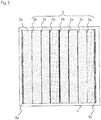
- Fig. 7 is a plan view showing the structure of organic electroluminescent lighting device 20 according to this embodiment.
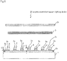
- Fig. 8 is a sectional view cut along line A2-A2 shown in Fig. 2 .
- some (interlayer insulating film 4, organic light-emitting film 5, and electrode film 2b) of the components of organic electroluminescent lighting device 20 are not shown.
- auxiliary electrode films 3a are equal in width. However, in relation to increasing distance from power supply terminal sections 6a and 6b, auxiliary electrode films 3a become thicker (refer to Fig. 8 ). Accordingly, as in the case of the first embodiment, in relation to increases in the distance from power supply terminal sections 6a and 6b, the sectional area of each of auxiliary electrode films 3a becomes larger. Similarly, auxiliary electrode films 3b are equal in width. However, in relation increasing distance from power supply terminal sections 6a and 6b, auxiliary electrode films 3b become thicker. Accordingly, as in the case of the first embodiment, in relation to increasing distance from power supply terminal sections 6a and 6b, the sectional area of each of auxiliary electrode films 3b becomes larger.
- auxiliary electrode films 3a and 3b formed as described above even when the voltage is applied from power supply terminal sections 6a and 6b to entire electrode film 2a, it is difficult for voltage drop to occur in the region that is separated from power supply terminal sections 6a and 6b. As a result, voltage distribution variance in electrode film 2a is prevented. This also prevents voltage distribution variance in organic light-emitting film 5. Thus, the brightness uniformity of organic light-emitting film 5 is improved.
- auxiliary electrode film 3a when thickness t1 (refer to Fig. 8 ) of auxiliary electrode film 3a that is formed closest to the center of electrode film 2a is excessively large, the step of auxiliary electrode film 3a is increased. Then, forming organic light-emitting film 5 and electrode film 2b after auxiliary electrode film 3a is easily made to have a non-uniform film thickness, which consequently increases the possibility that a short-circuit will occur between electrode film 2a and electrode film 2b. It is accordingly desirable to set thickness t1 to be three times larger, at a maximum, than thickness t3 (refer to Fig. 8 ) of auxiliary electrode film 3a that is formed closest to each of power supply terminal sections 6a and 6b.
- auxiliary electrode film 3b similarly, it is desirable to set the thickness of auxiliary electrode film 3b that is formed closest to the center of electrode film 2a to be three times larger, at a maximum, than the thickness of auxiliary electrode film 3b that is formed closest to each of power supply terminal sections 6a and 6b.
- a plurality of auxiliary electrode films 3c and 3d can be formed on the surface of electrode film 2b.
- the shapes of the plurality of auxiliary electrode films 3c and 3d can be similar to those of the first embodiment, or to those of auxiliary electrode films 3a and 3b of this embodiment.
- Organic electroluminescent lighting device 30 according to this embodiment will be described. Components similar to those of organic electroluminescent lighting device 10 according to the first embodiment are denoted by similar reference numerals, and thus detailed description thereof will be omitted.
- Fig. 9 is a plan view showing the structure of organic electroluminescent lighting device 30 according to this embodiment.
- some (interlayer insulating film 4, organic light-emitting film 5, and electrode film 2b) of the components of organic electroluminescent lighting device 30 are not shown.
- a plurality of auxiliary electrode films 3a are arranged at different intervals to extend in a direction parallel to edge sides of electrode film 2a.
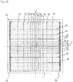
- a pattern of auxiliary electrode films 3a and 3b can be formed by taking symmetrical design into consideration so that a plurality of auxiliary electrode films 3a and 3b can be symmetrical with respect to first axis 1 and second axis m as shown in Fig. 10 .
- auxiliary electrode films 3a are similar in shape (width and thickness). supply terminal sections 6a and 6b. Accordingly, even when voltage is applied from power supply terminal sections 6a and 6b to entire electrode film 2a, it is difficult for voltage drop to occur in a region separated from power supply terminal sections 6a and 6b. As a result, voltage distribution variance in electrode film 2a is prevented. This also prevents voltage distribution variance in organic light-emitting film 5. Thus, the brightness uniformity of organic light-emitting film 5 is improved.
- auxiliary electrode films 3a and 3b formed with the pattern shown in Fig. 10 when the wiring density of auxiliary electrode film 3a near center C of electrode film 2a is excessively large, the light-emitting area is reduced (light shielding area by auxiliary electrode film 3a is larger), consequently lowering illuminance. It is accordingly desirable to set the wiring density of auxiliary electrode film 3a to be five times larger, at a maximum, than that of auxiliary electrode films 3a and 3b that are formed near power supply terminal sections 6a and 6b.
- auxiliary electrode films 3c similar in shape to auxiliary electrode film 3a of this embodiment can be formed on the surface of electrode film 2b.
- auxiliary electrode films 3a and 3b that have the shapes described in the first and second embodiments can be formed on the surface of electrode film 2b.
Landscapes
- Physics & Mathematics (AREA)
- Optics & Photonics (AREA)
- Electroluminescent Light Sources (AREA)
Description
- The present invention relates to an organic electroluminescent lighting device that uses, as a light source, a light-emitting element including an organic light-emitting film held between a pair of electrode films different from each other in polarity.
- One of the illumination devices is an organic electroluminescent lighting device that uses, as a light source, a light-emitting element including an organic light-emitting film held between a pair of electrode films different from each other in polarity. In the organic electroluminescent lighting device, the organic light-emitting film emits light when an electric field is generated between the pair of electrode films. The light of the organic light-emitting film is transmitted through one of the electrode films to be applied to the outside. Accordingly, one of the electrode films is made of a transparent metallic material such as ITO (indium tin oxide), ZnO, or SnO2 (NESA glass).
- However, the aforementioned transparent metallic material has relatively high resistance. Further, in the electrode film, generally, each of the opposite edge sides of its surface is a power supply terminal. Thus, in the electrode film, wiring resistance increases farther away from each edge side. The increase of the wiring resistance is accompanied by the increase of a descending voltage. This disables uniform application of a voltage to the entire organic light-emitting film. The brightness of the organic light-emitting film depends on the voltage. Thus, when the voltage is not uniformly applied to the organic light-emitting film, there is a possibility that the brightness of the organic light-emitting film is not uniform.
- Patent Literature 1 (
JP2004-14128A Patent Literature 1 includes auxiliary electrodes made of materials having a lower resistance than electrode and arranged on a grid pattern in the surface of the transparent electrode. According to this organic electroluminescent lighting device, the resistance value of the entire transparent electrode is reduced by forming, in the transparent electrode, auxiliary electrodes that have a lower resistance than the transparent electrode. The wiring resistance accordingly drops to reduce the value of the descending voltage. As a result, the brightness nonuniformity of the organic light-emitting film can be prevented. -
EP1484632 discloses a luminescent device for reducing unevenness of brightness. The luminescent device includes a transparent substrate, which has a light exit surface and an incident surface, and a luminescent element, which is formed on the incident surface of the transparent substrate. The luminescent element includes a transparent electrode formed on the incident surface of the transparent substrate, an auxiliary electrode formed on a part of the transparent electrode, and a thin-film layer, which is formed on the transparent electrode, for emitting light. The transparent substrate includes a projection formed on the light exit surface. The luminescent device may be used for backlighting an LCD panel. - Patent Literature 1:
JP2004-14128A - However, in the organic electroluminescent lighting device described in
Patent Literature 1, the auxiliary electrodes are similar in shape (width and film thickness) and arranged at equal intervals in the surface of the transparent electrode. Thus, when the voltage is applied to the entire transparent electrode from each of the edge sides of the transparent electrode, voltage reduction occurs more away from the edge side (closer to the center from the edge side). As a result, a voltage distribution varies in the transparent electrode, causing variance on a voltage distribution in the organic light-emitting film. Thus, brightness uniformity is insufficient in the organic electroluminescent lighting device described inPatent Literature 1. - It is therefore an object of the present invention to provide an organic electroluminescent lighting device that can improve brightness uniformity.
- To achieve the object, an organic electroluminescent lighting device according to a first aspect of the present invention includes:
an organic light-emitting film; - a pair of electrode films that are stacked to face each other sandwiching the organic light-emitting element; wherein the pair of electrode films are formed rectangular and differ from each other in polarity; wherein the pair of electrode films comprise power supply terminal sections which are connected to the power source; wherein power supply terminal sections each have edge sides which face each other at a surface of one of the electrode films; and
- an auxiliary electrode film group including a plurality of first belt-like auxiliary electrode films and a plurality of second belt-like auxiliary electrode films; wherein the first auxiliary electrode films extend in a direction parallel to the edge sides and the second auxiliary electrode films extend in a direction perpendicular to the edge sides; wherein the first auxiliary electrode films and the second auxiliary electrode films are located away from each other on the surface of one of the electrode films,
- In a further aspect of the invention there is provided an organic electroluminescent lighting device comprising:
- an organic light-emitting film;
- a pair of electrode films that are stacked to face each other sandwiching the organic light-emitting element; wherein the pair of electrode films are formed rectangular and differ from each other in polarity; wherein the pair of electrode films comprise power supply terminal sections which are connected to the power source; wherein power supply terminal sections each have edge sides which face each other at a surface of one of the electrode films; and
- an auxiliary electrode film group including a plurality of first belt-like auxiliary electrode films and a plurality of second belt-like auxiliary electrode films; wherein the first auxiliary electrode films extend in a direction parallel to the edge sides and the second auxiliary electrode films extend in a direction perpendicular to the edge sides; wherein the first auxiliary electrode films and the second auxiliary electrode films are located away from each other on the surface of one of the electrode films,
- wherein a wiring density which indicates the number of the plurality of first auxiliary electrode films on the surface of one of the electrode films becomes higher in relation to increasing distance from the edge side and a wiring density which indicates the number of the plurality of second auxiliary electrode films on the surface of one of the electrode films becomes higher in relation to increasing distance from the edge side;
- wherein the wiring density of the first auxiliary electrode film is five times larger, at a maximum, than that of the first and second auxiliary electrode films that are formed near the power supply terminal sections.
- The organic electroluminescent lighting device according to the first aspect, wherein a width of the first auxiliary electrode film becomes larger in relation to increasing distance from the edge side and a width of each of the plurality of second auxiliary electrodes films becomes larger in relation to increasing distance from the edge side.
- In certain embodiments the plurality of first auxiliary electrode films are formed symmetrical with respect to each of a first axis and a second axis extending; wherein the first axis extends in the direction parallel to the edge side and the second axis extends in the direction perpendicular to the edge side; wherein the first axis and the second axis orthogonally intersect each other in the center of the surface of one of the electrode films; wherein a width of each of the plurality of first auxiliary electrode films becomes larger in relation to approaching the second axis; wherein the plurality of second auxiliary electrode films is formed symmetrical with respect to each of the first axis and the second axis and a width of each of the plurality of second auxiliary electrode films becomes larger in relation to approaching the second axis.
- The organic electroluminescent lighting device according to the first aspect, wherein in relation to increasing distance from the edge side a film thickness of the first auxiliary electrode film becomes thicker and a film thickness of each of the plurality of second auxiliary electrode films becomes thicker in relation to increasing distance from the edge side.
- The organic electroluminescent lighting device according to any one of the aspects described herein,
further comprising other power supply terminal sections which are connected to the power source; wherein the other power supply terminal sections are other edge sides which face each other at the surface of the other electrode films; and
another auxiliary electrode film group including a plurality of third belt-like auxiliary electrode films and a plurality of fourth belt-like auxiliary electrode films; wherein the third auxiliary electrode films extend in a direction parallel to the other edge sides and the fourth auxiliary electrode films extend in a direction perpendicular to the edge sides; wherein the third auxiliary electrode films and the fourth auxiliary electrode films are located away from each other on the surface of the other electrode films,
wherein a sectional area viewed at a section where the plurality of third auxiliary electrode films is cut in the direction perpendicular to the edge sides becomes larger in relation to increasing distance from the other edge sides and a sectional area viewed at a section where the plurality of fourth auxiliary electrode films is cut in the direction parallel to the edge sides becomes larger in relation to increasing distance from the other edge side. - According to the present invention, in one of the electrode films, in relation to increasing distance from each of the edge sides, the sectional area of at least one of the first auxiliary electrode film and the second auxiliary electrode film becomes larger, or the wiring density of the first auxiliary electrode film becomes higher. Thus, when a voltage is applied from each of the edge sides to the entire electrode film, it is difficult for voltage drop to occur in a region away from the edge side. As a result, since voltage distribution variance in the electrode film is prevented, voltage distribution variance in the organic light-emitting film can also be prevented. Thus, brightness uniformity is improved.
-
- [
Fig. 1 ] A plan view showing the structure of an organic electroluminescent lighting device according to a first embodiment. - [
Fig. 2 ] A sectional view cut along line A1-A1 shown inFig. 1 . - [
Fig. 3 ] A plan view showing another arrangement pattern of auxiliary electrode films in the organic electroluminescent lighting device according to the first embodiment. - [
Fig. 4 ] A plan view showing yet another arrangement pattern of the auxiliary electrode films in the organic electroluminescent lighting device according to the first embodiment. - [
Fig. 5 ] A plan view showing yet another arrangement pattern of the auxiliary electrode films in the organic electroluminescent lighting device according to the first embodiment. - [
Fig. 6 ] A plan view showing still yet another arrangement pattern of the auxiliary electrode films in the organic electroluminescent lighting device according to the first embodiment. - [
Fig. 7 ] A plan view showing the structure of an organic electroluminescent lighting device according to a second embodiment. - [
Fig. 8 ] A sectional view cut along line A2-A2 shown inFig. 7 . - [
Fig. 9 ] A plan view showing the structure of an organic electroluminescent lighting device according to a third embodiment. - [
Fig. 10 ] A plan view showing another arrangement pattern of auxiliary electrode films in the organic electroluminescent lighting device according to the third embodiment. -
Fig. 1 is a plan view showing the structure of organicelectroluminescent lighting device 10 according to this embodiment.Fig. 2 is a sectional view cut along line A1-A1 shown inFig. 1 . InFig. 1 , for easier understanding, some (interlayer insulating film 4, organic light-emittingfilm 5, andelectrode film 2b) of the components of organicelectroluminescent lighting device 10 are not shown. - In organic
electroluminescent lighting device 10, as shown inFig. 2 ,rectangular electrode film 2a is formed on the surface oftransparent substrate 1.Transparent substrate 1 is a glass substrate or a plastic substrate.Electrode film 2a is a positive electrode made of a transparent metallic material such as ITO, ZnO, or SnO2 (NESA glass). Edge sides opposite each other on the surface ofelectrode film 2a are powersupply terminal sections - Auxiliary
electrode film group 3 including a plurality of belt-likeauxiliary electrode films 3a (first auxiliary electrode films) and a plurality of belt-likeauxiliary electrode films 3b (second auxiliary electrode films) are formed on the surface ofelectrode film 2a. The plurality ofauxiliary electrode films 3a are located away from each other to extend in a direction parallel to powersupply terminal sections auxiliary electrode films 3a) as shown inFig. 1 . In relation to increasing distance from powersupply terminal sections auxiliary electrode films 3a becomes larger. - On the other hand, the plurality of
auxiliary electrode films 3b are located away from each other to extend in a direction perpendicular to powersupply terminal sections supply terminal sections auxiliary electrode films 3b becomes gradually larger. In relation to increasing distance from powersupply terminal sections auxiliary electrode films 3b can become continuously larger. -
Auxiliary electrode films electrode film 2a, such as Cr (chromium), Al-Nd (aluminum-neodymium alloy), or Mo-Nb (molybdenum-niobium alloy).Auxiliary electrode films electrode film group 3 is not limited to a grid pattern shown inFig. 1 . For example, as shown inFig. 3 , auxiliaryelectrode film group 3 can have an arrangement pattern including only a plurality ofauxiliary electrode films 3a. Further, as shown inFig. 4 , auxiliaryelectrode film group 3 can have an arrangement pattern including only a plurality ofauxiliary electrode films 3b. In this embodiment, since the plurality ofauxiliary electrode films 3b is thought to function as a light shielding part, a pattern of auxiliaryelectrode film group 3 can be formed by taking design (symmetry) into consideration, as shown inFig. 5 . InFig. 5 , the plurality ofauxiliary electrode films 3a is formed to be symmetrical with respect tofirst axis 1 extending in the direction parallel to powersupply terminal sections supply terminal sections electrode film 2a. In relation to approaching a second axis m, the width ofauxiliary electrode films 3a becomes larger.Auxiliary electrode films 3b are also formed to be symmetrical with respect tofirst axis 1 and second axis m, and wider closer to second axis m. In the present invention, the pluralities ofauxiliary electrode films electrode film 2a that is in contacted withtransparent substrate 1. - The surfaces of the pluralities of
auxiliary electrode films Fig. 4 ) to prevent insulation degradation of organic light-emittingfilm 5. The surface ofinterlayer insulating film 4 is covered with organic light-emitting film 5 (refer toFig. 2 ). In the present invention, there is no particular limitation on materials forinterlayer insulating film 4 and organic light-emittingfilm 5. Conventional materials can be used. The surface of organic light-emittingfilm 5 is covered withelectrode film 2b (refer toFig. 2 ) which pairs withelectrode film 2a. In this embodiment,electrode film 2b is a negative electrode made of a material whose resistance is lower thanelectrode film 2a, such as aluminum. - In the organic electroluminescent lighting device which does not comprise auxiliary
electrode film group 3, when a voltage is applied from the light source through powersupply terminal sections entire electrode film 2a, in relation to increasing distance from powersupply terminal sections electrode film 2a), a potential becomes lower. However, in this embodiment, in relation to increasing distance from powersupply terminal sections auxiliary electrode films 3a becomes larger. Accordingly, a sectional area viewed at a section where the plurality ofauxiliary electrode films 3a is cut in the direction perpendicular to powersupply terminal sections auxiliary electrode film 3a that is separated from the powersupply terminal sections supply terminal sections auxiliary electrode films 3b becomes larger. Accordingly, a sectional area viewed at a section where the plurality ofauxiliary electrode films 3b is cut in the direction parallel to powersupply terminal sections supply terminal sections - Because of
auxiliary electrode films supply terminal sections entire electrode film 2a, it is difficult for a voltage drop to occur in the region separated from powersupply terminal sections electrode film 2a is prevented. This also prevents voltage distribution variance in organic light-emittingfilm 5. Thus, the brightness uniformity of organic light-emittingfilm 5 is improved. - In this embodiment, when width W1 (refer to
Fig. 2 ) ofauxiliary electrode film 3a formed closest to the center ofelectrode film 2a is excessively large, a light-emitting area is reduced (light shielding area byauxiliary electrode film 3a is increased), consequently lowering illuminance. It is accordingly desirable to set width W1 to be five times larger, at a maximum, than width W3 (refer toFig. 2 ) ofauxiliary electrode film 3a that is formed closest to each of powersupply terminal sections auxiliary electrode film 3b, similarly, it is desirable to set the width ofauxiliary electrode film 3b formed closest to the center ofelectrode film 2a to be five times larger, at a maximum, than the width ofauxiliary electrode film 3b that is formed closest to each of powersupply terminal sections - In this embodiment, the plurality of
auxiliary electrode films electrode film 2a. However, they can be formed on the surface ofelectrode film 2b, or on the surfaces of both ofelectrode films electrode film 2b on which the auxiliary electrode films are formed can be a surface that is in contacted with organic light-emittingfilm 5, or that faces (opposite) the surface ofelectrode film 2b. -
Fig. 6 is a plan view showing an example ofelectrode film 2b in which auxiliary electrode films are formed. InFig. 6 , the opposing edge sides of the surface ofelectrode film 2b are powersupply terminal sections electrode film 2b, as in the case ofelectrode film 2a, a plurality of belt-likeauxiliary electrode films 3c (third auxiliary electrode films) and a plurality of belt-likeauxiliary electrode films 3d (fourth auxiliary electrode films) are formed. The plurality ofauxiliary electrode films 3c extends in a direction parallel to powersupply terminal sections auxiliary electrode films 3d extends in a direction perpendicular to powersupply terminal sections auxiliary electrode films electrode film 2b. However, it is desirable to use materials whose resistance is lower than those ofelectrode film 2b. This is because the resistance ofentire electrode film 2b is reduced. Specifically, in the case of formingelectrode film 2b made of aluminum, Ag, Au, or Cu is used. When Ag or Au is used,auxiliary electrode films film 5. Further, when Cu is used as materials for the auxiliary electrode films, the auxiliary electrode films are formed by sputtering or CVD (chemical vapor deposition). The melting point of Cu is relatively high. Thus, it is difficult for electro migration to occur, and it is also difficult for stress migration to occur. - Organic
electroluminescent lighting device 20 according to this embodiment will be described. Components similar to those of organicelectroluminescent lighting device 10 according to the first embodiment are denoted by similar reference numerals, and thus detailed description thereof will be omitted. -
Fig. 7 is a plan view showing the structure of organicelectroluminescent lighting device 20 according to this embodiment.Fig. 8 is a sectional view cut along line A2-A2 shown inFig. 2 . InFig. 7 , for easier understanding, some (interlayer insulating film 4, organic light-emittingfilm 5, andelectrode film 2b) of the components of organicelectroluminescent lighting device 20 are not shown. - In this embodiment,
auxiliary electrode films 3a are equal in width. However, in relation to increasing distance from powersupply terminal sections auxiliary electrode films 3a become thicker (refer toFig. 8 ). Accordingly, as in the case of the first embodiment, in relation to increases in the distance from powersupply terminal sections auxiliary electrode films 3a becomes larger. Similarly,auxiliary electrode films 3b are equal in width. However, in relation increasing distance from powersupply terminal sections auxiliary electrode films 3b become thicker. Accordingly, as in the case of the first embodiment, in relation to increasing distance from powersupply terminal sections auxiliary electrode films 3b becomes larger. - Because of
auxiliary electrode films supply terminal sections entire electrode film 2a, it is difficult for voltage drop to occur in the region that is separated from powersupply terminal sections electrode film 2a is prevented. This also prevents voltage distribution variance in organic light-emittingfilm 5. Thus, the brightness uniformity of organic light-emittingfilm 5 is improved. - In this embodiment, when thickness t1 (refer to
Fig. 8 ) ofauxiliary electrode film 3a that is formed closest to the center ofelectrode film 2a is excessively large, the step ofauxiliary electrode film 3a is increased. Then, forming organic light-emittingfilm 5 andelectrode film 2b afterauxiliary electrode film 3a is easily made to have a non-uniform film thickness, which consequently increases the possibility that a short-circuit will occur betweenelectrode film 2a andelectrode film 2b. It is accordingly desirable to set thickness t1 to be three times larger, at a maximum, than thickness t3 (refer toFig. 8 ) ofauxiliary electrode film 3a that is formed closest to each of powersupply terminal sections auxiliary electrode film 3b, similarly, it is desirable to set the thickness ofauxiliary electrode film 3b that is formed closest to the center ofelectrode film 2a to be three times larger, at a maximum, than the thickness ofauxiliary electrode film 3b that is formed closest to each of powersupply terminal sections - In this embodiment, a plurality of
auxiliary electrode films electrode film 2b. The shapes of the plurality ofauxiliary electrode films auxiliary electrode films - Organic
electroluminescent lighting device 30 according to this embodiment will be described. Components similar to those of organicelectroluminescent lighting device 10 according to the first embodiment are denoted by similar reference numerals, and thus detailed description thereof will be omitted. -
Fig. 9 is a plan view showing the structure of organicelectroluminescent lighting device 30 according to this embodiment. InFig. 9 , for easier understanding, some (interlayer insulating film 4, organic light-emittingfilm 5, andelectrode film 2b) of the components of organicelectroluminescent lighting device 30 are not shown. - In organic
electroluminescent lighting device 30 according to this embodiment, a plurality ofauxiliary electrode films 3a are arranged at different intervals to extend in a direction parallel to edge sides ofelectrode film 2a. In this embodiment, a pattern ofauxiliary electrode films auxiliary electrode films first axis 1 and second axis m as shown inFig. 10 . - In this embodiment,
auxiliary electrode films 3a are similar in shape (width and thickness).supply terminal sections supply terminal sections entire electrode film 2a, it is difficult for voltage drop to occur in a region separated from powersupply terminal sections electrode film 2a is prevented. This also prevents voltage distribution variance in organic light-emittingfilm 5. Thus, the brightness uniformity of organic light-emittingfilm 5 is improved. - In this embodiment, in the case of
auxiliary electrode films Fig. 10 , when the wiring density ofauxiliary electrode film 3a near center C ofelectrode film 2a is excessively large, the light-emitting area is reduced (light shielding area byauxiliary electrode film 3a is larger), consequently lowering illuminance. It is accordingly desirable to set the wiring density ofauxiliary electrode film 3a to be five times larger, at a maximum, than that ofauxiliary electrode films supply terminal sections - In this embodiment, a plurality of
auxiliary electrode films 3c similar in shape toauxiliary electrode film 3a of this embodiment can be formed on the surface ofelectrode film 2b. Alternatively,auxiliary electrode films electrode film 2b. - The embodiments of the present invention have been described. However, the present invention is not limited to the embodiments. Various changes understandable to those skilled in the art can be made to the configuration and the specifics of the present invention.
- This application claims priority from Japanese Patent Application No.
2010-130009 filed June 7, 2010 -
- 1 Transparent substrate
- 2a, 2b Electrode film
- 3 Auxiliary electrode film group
- 3a, 3b, 3c, 3d Auxiliary electrode film
- 4 Interlayer insulating film
- 5 Organic light-emitting film
- 6a, 6b, 6c, 6d Power supply terminal section
- 10, 20, 30 Organic electroluminescent lighting device
Claims (6)
- An organic electroluminescent lighting device (10, 20, 30) comprising:an organic light-emitting film (5);a pair of electrode films (2a, 2b) that are stacked to face each other sandwiching the organic light-emitting element; wherein the pair of electrode films are formed rectangular and differ from each other in polarity; wherein the pair of electrode films comprise power supply terminal sections (6a, 6b, 6c, 6d) which are connected to the power source; wherein power supply terminal sections each have edge sides which face each other at a surface of one of the electrode films; andan auxiliary electrode film group (3) including a plurality of first belt-like auxiliary electrode films (3a, 3b, 3c, 3d) and a plurality of second belt-like auxiliary electrode films (3a, 3b, 3c, 3d); wherein the first auxiliary electrode films extend in a direction parallel to the edge sides and the second auxiliary electrode films extend in a direction perpendicular to the edge sides; wherein the first auxiliary electrode films and the second auxiliary electrode films are located away from each other on the surface of one of the electrode films,wherein a sectional area viewed at a section where the plurality of first auxiliary electrode films is cut in the direction perpendicular to the edge sides becomes larger in relation to increasing distance from the edge sides, and a sectional area viewed at a section where the plurality of second auxiliary electrode films is cut in the direction parallel to the edge sides becomes larger in relation to increasing distance from the edge sides.
- An organic electroluminescent lighting device (10, 20, 30) comprising:an organic light-emitting film (5);a pair of electrode films (2a, 2b) that are stacked to face each other sandwiching the organic light-emitting element; wherein the pair of electrode films are formed rectangular and differ from each other in polarity; wherein the pair of electrode films comprise power supply terminal sections (6a, 6b, 6c, 6d) which are connected to the power source; wherein power supply terminal sections each have edge sides which face each other at a surface of one of the electrode films; andan auxiliary electrode film group (3) including a plurality of first belt-like auxiliary electrode films (3a, 3b, 3c, 3d) and a plurality of second belt-like auxiliary electrode films (3a, 3b, 3c, 3d); wherein the first auxiliary electrode films extend in a direction parallel to the edge sides and the second auxiliary electrode films extend in a direction perpendicular to the edge sides; wherein the first auxiliary electrode films and the second auxiliary electrode films are located away from each other on the surface of one of the electrode films,wherein a wiring density which indicates the number of the plurality of first auxiliary electrode films on the surface of one of the electrode films becomes higher in relation to increasing distance from the edge side and a wiring density which indicates the number of the plurality of second auxiliary electrode films on the surface of one of the electrode films becomes higher in relation to increasing distance from the edge side;wherein the wiring density of the first auxiliary electrode film is five times larger, at a maximum, than that of the first and second auxiliary electrode films that are formed near the power supply terminal sections.
- The organic electroluminescent lighting device (10, 20, 30) according to claim 1, wherein a width of the first auxiliary electrode film (3a, 3b, 3c, 3d) becomes larger in relation to increasing distance from the edge side and a width of each of the plurality of second auxiliary electrodes films (3a, 3b, 3c, 3d) becomes larger in relation to increasing distance from the edge side.
- The organic electroluminescent lighting device (10, 20, 30) according to claim 3, wherein the plurality of first auxiliary electrode films (3a, 3b, 3c, 3d) are formed symmetrical with respect to each of a first axis and a second axis extending; wherein the first axis extends in the direction parallel to the edge side and the second axis extends in the direction perpendicular to the edge side; wherein the first axis and the second axis orthogonally intersect each other in the center of the surface of one of the electrode films; wherein a width of each of the plurality of first auxiliary electrode films becomes larger in relation to approaching the second axis; wherein the plurality of second auxiliary electrode films (3a, 3b, 3c, 3d) is formed symmetrical with respect to each of the first axis and the second axis and a width of each of the plurality of second auxiliary electrode films becomes larger in relation to approaching the second axis.
- The organic electroluminescent lighting device (10, 20, 30) according to claim 1, wherein in relation to increasing distance from the edge side a film thickness of the first auxiliary electrode film (3a, 3b, 3c, 3d) becomes thicker and a film thickness of each of the plurality of second auxiliary electrode films (3a, 3b, 3c, 3d) becomes thicker in relation to increasing distance from the edge side.
- The organic electroluminescent lighting device (10, 20, 30) according to any one of claims 1 to 5,
further comprising other power supply terminal sections (6a, 6b, 6c, 6d) which are connected to the power source; wherein the other power supply terminal sections are other edge sides which face each other at the surface of the other electrode films; and
another auxiliary electrode film group (3) including a plurality of third belt-like auxiliary electrode films (3a, 3b, 3c, 3d) and a plurality of fourth belt-like auxiliary electrode films (3a, 3b, 3c, 3d); wherein the third auxiliary electrode films extend in a direction parallel to the other edge sides and the fourth auxiliary electrode films extend in a direction perpendicular to the edge sides; wherein the third auxiliary electrode films and the fourth auxiliary electrode films are located away from each other on the surface of the other electrode films,
wherein a sectional area viewed at a section where the plurality of third auxiliary electrode films is cut in the direction perpendicular to the edge sides becomes larger in relation to increasing distance from the other edge sides and a sectional area viewed at a section where the plurality of fourth auxiliary electrode films is cut in the direction parallel to the edge sides becomes larger in relation to increasing distance from the other edge side.
Applications Claiming Priority (2)
| Application Number | Priority Date | Filing Date | Title |
|---|---|---|---|
| JP2010130009 | 2010-06-07 | ||
| PCT/JP2011/061638 WO2011155306A1 (en) | 2010-06-07 | 2011-05-20 | Organic electroluminescent illumination device |
Publications (3)
| Publication Number | Publication Date |
|---|---|
| EP2560462A1 EP2560462A1 (en) | 2013-02-20 |
| EP2560462A4 EP2560462A4 (en) | 2016-10-26 |
| EP2560462B1 true EP2560462B1 (en) | 2019-02-27 |
Family
ID=45097915
Family Applications (1)
| Application Number | Title | Priority Date | Filing Date |
|---|---|---|---|
| EP11792264.1A Not-in-force EP2560462B1 (en) | 2010-06-07 | 2011-05-20 | Organic electroluminescent illumination device |
Country Status (4)
| Country | Link |
|---|---|
| US (1) | US8659220B2 (en) |
| EP (1) | EP2560462B1 (en) |
| JP (1) | JPWO2011155306A1 (en) |
| WO (1) | WO2011155306A1 (en) |
Families Citing this family (17)
| Publication number | Priority date | Publication date | Assignee | Title |
|---|---|---|---|---|
| WO2012160468A1 (en) * | 2011-05-23 | 2012-11-29 | Koninklijke Philips Electronics N.V. | Fabrication apparatus for fabricating a patterned layer |
| US20150060799A1 (en) * | 2012-03-13 | 2015-03-05 | Panasonic Corporation | Organic electroluminescent element |
| JP5907766B2 (en) * | 2012-03-14 | 2016-04-26 | 株式会社カネカ | Light emitting device and method for manufacturing light emitting device |
| WO2014073072A1 (en) * | 2012-11-08 | 2014-05-15 | パイオニア株式会社 | Mirror device |
| JP6249340B2 (en) * | 2013-02-07 | 2017-12-20 | パナソニックIpマネジメント株式会社 | ORGANIC ELECTROLUMINESCENT ELEMENT AND LIGHTING DEVICE |
| GB201314793D0 (en) | 2013-08-19 | 2013-10-02 | Cambridge Display Tech Ltd | Lighting tiles |
| DE102014110969A1 (en) | 2014-08-01 | 2016-02-04 | Osram Oled Gmbh | Organic component and method for producing an organic component |
| EP3236507B1 (en) * | 2014-12-15 | 2021-09-01 | LG Display Co., Ltd. | Organic light-emitting device |
| JP6640450B2 (en) * | 2015-01-26 | 2020-02-05 | パイオニア株式会社 | Light emitting device |
| JP6657181B2 (en) * | 2015-03-25 | 2020-03-04 | パイオニア株式会社 | Light emitting device |
| CN104867450B (en) * | 2015-06-05 | 2017-09-19 | 京东方科技集团股份有限公司 | Array base palte and preparation method thereof, display device |
| KR102560268B1 (en) * | 2015-12-31 | 2023-07-27 | 엘지디스플레이 주식회사 | Organic light emitting diode display device |
| KR102068870B1 (en) | 2016-06-17 | 2020-01-21 | 주식회사 엘지화학 | Electrode structure, electronic device comprising the same and manufacturing method thereof |
| JP2018073526A (en) * | 2016-10-26 | 2018-05-10 | パイオニア株式会社 | Light emitting device |
| JP6893020B2 (en) * | 2017-04-05 | 2021-06-23 | 株式会社Joled | Manufacturing method of organic EL display panel and organic EL display panel |
| KR102413156B1 (en) * | 2017-11-28 | 2022-06-24 | 엘지디스플레이 주식회사 | Light apparatus for organic light emitting device |
| JP2020053409A (en) * | 2019-12-26 | 2020-04-02 | パイオニア株式会社 | Light emitting device |
Family Cites Families (15)
| Publication number | Priority date | Publication date | Assignee | Title |
|---|---|---|---|---|
| KR100267964B1 (en) * | 1998-07-20 | 2000-10-16 | 구자홍 | Organic electroluminescent display panel and method for fabricating the same |
| JP4599685B2 (en) * | 2000-08-04 | 2010-12-15 | ソニー株式会社 | Flat display element |
| JP3864851B2 (en) | 2002-06-03 | 2007-01-10 | 株式会社豊田自動織機 | Planar light emitting device |
| US7026658B2 (en) * | 2003-03-13 | 2006-04-11 | Samsung Sdi, Co., Ltd. | Electrical conductors in an electroluminescent display device |
| JP4114551B2 (en) | 2003-06-06 | 2008-07-09 | 株式会社豊田自動織機 | Planar light emitting device using auxiliary electrode |
| JP4561490B2 (en) * | 2004-12-24 | 2010-10-13 | 株式会社豊田自動織機 | Electroluminescence element |
| JP2007080579A (en) * | 2005-09-12 | 2007-03-29 | Toyota Industries Corp | Surface emitting device |
| TW200808119A (en) * | 2006-06-28 | 2008-02-01 | Sumitomo Chemical Co | Organic electroluminescence device |
| KR100811473B1 (en) | 2006-10-17 | 2008-03-07 | 엘지전자 주식회사 | Electroluminescent panel and light source device including the same |
| JP5060845B2 (en) * | 2007-06-27 | 2012-10-31 | 株式会社ジャパンディスプレイイースト | Screen input type image display device |
| KR101222990B1 (en) * | 2007-10-22 | 2013-01-18 | 엘지디스플레이 주식회사 | Liquid Crystal Lens Electrically driven and Stereoscopy Display Device |
| JP2010009584A (en) * | 2008-05-29 | 2010-01-14 | Sony Corp | Display device |
| JP5314385B2 (en) * | 2008-10-31 | 2013-10-16 | 住友化学株式会社 | Method for manufacturing organic electroluminescence element |
| JP5227773B2 (en) | 2008-12-18 | 2013-07-03 | 財団法人山形県産業技術振興機構 | Organic EL panel mounting device |
| JP2010244885A (en) * | 2009-04-07 | 2010-10-28 | Panasonic Corp | Organic electroluminescence image display device and manufacturing method thereof |
-
2011
- 2011-05-20 JP JP2012519324A patent/JPWO2011155306A1/en active Pending
- 2011-05-20 WO PCT/JP2011/061638 patent/WO2011155306A1/en not_active Ceased
- 2011-05-20 US US13/698,845 patent/US8659220B2/en not_active Expired - Fee Related
- 2011-05-20 EP EP11792264.1A patent/EP2560462B1/en not_active Not-in-force
Non-Patent Citations (1)
| Title |
|---|
| None * |
Also Published As
| Publication number | Publication date |
|---|---|
| JPWO2011155306A1 (en) | 2013-08-01 |
| US20130093316A1 (en) | 2013-04-18 |
| US8659220B2 (en) | 2014-02-25 |
| WO2011155306A1 (en) | 2011-12-15 |
| EP2560462A4 (en) | 2016-10-26 |
| EP2560462A1 (en) | 2013-02-20 |
Similar Documents
| Publication | Publication Date | Title |
|---|---|---|
| US8659220B2 (en) | Organic electroluminescent lighting device | |
| US10186562B2 (en) | Thin film transistor and manufacturing method thereof, array substrate and organic light emitting display panel | |
| KR100752973B1 (en) | Electroluminescence element | |
| KR101994657B1 (en) | Organic electroluminescent display | |
| TWI552403B (en) | Large area light emitting electrical package with current spreading bus | |
| US10978532B2 (en) | Organic light-emitting diode (OLED) display panel and method thereof | |
| CN104953044A (en) | Flexible oled and manufacturing method thereof | |
| US8293570B2 (en) | Method for manufacturing light emitting device | |
| US9680125B2 (en) | Organic electroluminescent lighting device and method for manufacturing the same | |
| EP2627156B1 (en) | Organic electroluminescent lighting device and method for manufacturing said lighting device | |
| TWI451179B (en) | Pixel structure and its manufacturing method | |
| US9166187B2 (en) | Organic light emitting device and power supply device thereof | |
| TW201429016A (en) | Organic light-emitting diode device | |
| US10094534B2 (en) | Surface-emitting unit having dimming regions | |
| KR20060038067A (en) | Organic electroluminescent display device and manufacturing method thereof | |
| JP2014229546A (en) | Surface light-emitting unit and method for manufacturing the same | |
| JP5700185B1 (en) | Planar light emitting unit | |
| KR102353359B1 (en) | Transparent electrode and manufacturing method of the same | |
| US20160181326A1 (en) | Radiation-Emitting Apparatus and Method for Producing Same | |
| CN102623645B (en) | organic electroluminescent element | |
| CN103219475B (en) | The manufacture method of el light emitting device and the manufacture method of electrode base board thereof | |
| CN102097452A (en) | Light source device | |
| KR20110039062A (en) | Organic light emitting display | |
| KR100692051B1 (en) | Organic electroluminescent display and manufacturing method | |
| CN119233714A (en) | Display panel and display device |
Legal Events
| Date | Code | Title | Description |
|---|---|---|---|
| PUAI | Public reference made under article 153(3) epc to a published international application that has entered the european phase |
Free format text: ORIGINAL CODE: 0009012 |
|
| 17P | Request for examination filed |
Effective date: 20121116 |
|
| AK | Designated contracting states |
Kind code of ref document: A1 Designated state(s): AL AT BE BG CH CY CZ DE DK EE ES FI FR GB GR HR HU IE IS IT LI LT LU LV MC MK MT NL NO PL PT RO RS SE SI SK SM TR |
|
| DAX | Request for extension of the european patent (deleted) | ||
| RA4 | Supplementary search report drawn up and despatched (corrected) |
Effective date: 20160926 |
|
| RIC1 | Information provided on ipc code assigned before grant |
Ipc: F21Y 105/00 20160101ALI20160920BHEP Ipc: H05B 33/06 20060101ALI20160920BHEP Ipc: H05B 33/26 20060101AFI20160920BHEP Ipc: H01L 51/50 20060101ALI20160920BHEP |
|
| STAA | Information on the status of an ep patent application or granted ep patent |
Free format text: STATUS: EXAMINATION IS IN PROGRESS |
|
| 17Q | First examination report despatched |
Effective date: 20170620 |
|
| GRAP | Despatch of communication of intention to grant a patent |
Free format text: ORIGINAL CODE: EPIDOSNIGR1 |
|
| STAA | Information on the status of an ep patent application or granted ep patent |
Free format text: STATUS: GRANT OF PATENT IS INTENDED |
|
| INTG | Intention to grant announced |
Effective date: 20181022 |
|
| GRAS | Grant fee paid |
Free format text: ORIGINAL CODE: EPIDOSNIGR3 |
|
| GRAA | (expected) grant |
Free format text: ORIGINAL CODE: 0009210 |
|
| STAA | Information on the status of an ep patent application or granted ep patent |
Free format text: STATUS: THE PATENT HAS BEEN GRANTED |
|
| AK | Designated contracting states |
Kind code of ref document: B1 Designated state(s): AL AT BE BG CH CY CZ DE DK EE ES FI FR GB GR HR HU IE IS IT LI LT LU LV MC MK MT NL NO PL PT RO RS SE SI SK SM TR |
|
| REG | Reference to a national code |
Ref country code: GB Ref legal event code: FG4D |
|
| REG | Reference to a national code |
Ref country code: CH Ref legal event code: EP |
|
| REG | Reference to a national code |
Ref country code: AT Ref legal event code: REF Ref document number: 1103285 Country of ref document: AT Kind code of ref document: T Effective date: 20190315 |
|
| REG | Reference to a national code |
Ref country code: IE Ref legal event code: FG4D |
|
| REG | Reference to a national code |
Ref country code: DE Ref legal event code: R096 Ref document number: 602011056669 Country of ref document: DE |
|
| REG | Reference to a national code |
Ref country code: NL Ref legal event code: MP Effective date: 20190227 |
|
| REG | Reference to a national code |
Ref country code: LT Ref legal event code: MG4D |
|
| PG25 | Lapsed in a contracting state [announced via postgrant information from national office to epo] |
Ref country code: NO Free format text: LAPSE BECAUSE OF FAILURE TO SUBMIT A TRANSLATION OF THE DESCRIPTION OR TO PAY THE FEE WITHIN THE PRESCRIBED TIME-LIMIT Effective date: 20190527 Ref country code: FI Free format text: LAPSE BECAUSE OF FAILURE TO SUBMIT A TRANSLATION OF THE DESCRIPTION OR TO PAY THE FEE WITHIN THE PRESCRIBED TIME-LIMIT Effective date: 20190227 Ref country code: SE Free format text: LAPSE BECAUSE OF FAILURE TO SUBMIT A TRANSLATION OF THE DESCRIPTION OR TO PAY THE FEE WITHIN THE PRESCRIBED TIME-LIMIT Effective date: 20190227 Ref country code: PT Free format text: LAPSE BECAUSE OF FAILURE TO SUBMIT A TRANSLATION OF THE DESCRIPTION OR TO PAY THE FEE WITHIN THE PRESCRIBED TIME-LIMIT Effective date: 20190627 Ref country code: LT Free format text: LAPSE BECAUSE OF FAILURE TO SUBMIT A TRANSLATION OF THE DESCRIPTION OR TO PAY THE FEE WITHIN THE PRESCRIBED TIME-LIMIT Effective date: 20190227 Ref country code: NL Free format text: LAPSE BECAUSE OF FAILURE TO SUBMIT A TRANSLATION OF THE DESCRIPTION OR TO PAY THE FEE WITHIN THE PRESCRIBED TIME-LIMIT Effective date: 20190227 |
|
| PG25 | Lapsed in a contracting state [announced via postgrant information from national office to epo] |
Ref country code: LV Free format text: LAPSE BECAUSE OF FAILURE TO SUBMIT A TRANSLATION OF THE DESCRIPTION OR TO PAY THE FEE WITHIN THE PRESCRIBED TIME-LIMIT Effective date: 20190227 Ref country code: HR Free format text: LAPSE BECAUSE OF FAILURE TO SUBMIT A TRANSLATION OF THE DESCRIPTION OR TO PAY THE FEE WITHIN THE PRESCRIBED TIME-LIMIT Effective date: 20190227 Ref country code: IS Free format text: LAPSE BECAUSE OF FAILURE TO SUBMIT A TRANSLATION OF THE DESCRIPTION OR TO PAY THE FEE WITHIN THE PRESCRIBED TIME-LIMIT Effective date: 20190627 Ref country code: GR Free format text: LAPSE BECAUSE OF FAILURE TO SUBMIT A TRANSLATION OF THE DESCRIPTION OR TO PAY THE FEE WITHIN THE PRESCRIBED TIME-LIMIT Effective date: 20190528 Ref country code: RS Free format text: LAPSE BECAUSE OF FAILURE TO SUBMIT A TRANSLATION OF THE DESCRIPTION OR TO PAY THE FEE WITHIN THE PRESCRIBED TIME-LIMIT Effective date: 20190227 Ref country code: BG Free format text: LAPSE BECAUSE OF FAILURE TO SUBMIT A TRANSLATION OF THE DESCRIPTION OR TO PAY THE FEE WITHIN THE PRESCRIBED TIME-LIMIT Effective date: 20190527 |
|
| REG | Reference to a national code |
Ref country code: AT Ref legal event code: MK05 Ref document number: 1103285 Country of ref document: AT Kind code of ref document: T Effective date: 20190227 |
|
| PG25 | Lapsed in a contracting state [announced via postgrant information from national office to epo] |
Ref country code: DK Free format text: LAPSE BECAUSE OF FAILURE TO SUBMIT A TRANSLATION OF THE DESCRIPTION OR TO PAY THE FEE WITHIN THE PRESCRIBED TIME-LIMIT Effective date: 20190227 Ref country code: IT Free format text: LAPSE BECAUSE OF FAILURE TO SUBMIT A TRANSLATION OF THE DESCRIPTION OR TO PAY THE FEE WITHIN THE PRESCRIBED TIME-LIMIT Effective date: 20190227 Ref country code: EE Free format text: LAPSE BECAUSE OF FAILURE TO SUBMIT A TRANSLATION OF THE DESCRIPTION OR TO PAY THE FEE WITHIN THE PRESCRIBED TIME-LIMIT Effective date: 20190227 Ref country code: CZ Free format text: LAPSE BECAUSE OF FAILURE TO SUBMIT A TRANSLATION OF THE DESCRIPTION OR TO PAY THE FEE WITHIN THE PRESCRIBED TIME-LIMIT Effective date: 20190227 Ref country code: RO Free format text: LAPSE BECAUSE OF FAILURE TO SUBMIT A TRANSLATION OF THE DESCRIPTION OR TO PAY THE FEE WITHIN THE PRESCRIBED TIME-LIMIT Effective date: 20190227 Ref country code: ES Free format text: LAPSE BECAUSE OF FAILURE TO SUBMIT A TRANSLATION OF THE DESCRIPTION OR TO PAY THE FEE WITHIN THE PRESCRIBED TIME-LIMIT Effective date: 20190227 Ref country code: AL Free format text: LAPSE BECAUSE OF FAILURE TO SUBMIT A TRANSLATION OF THE DESCRIPTION OR TO PAY THE FEE WITHIN THE PRESCRIBED TIME-LIMIT Effective date: 20190227 Ref country code: SK Free format text: LAPSE BECAUSE OF FAILURE TO SUBMIT A TRANSLATION OF THE DESCRIPTION OR TO PAY THE FEE WITHIN THE PRESCRIBED TIME-LIMIT Effective date: 20190227 |
|
| REG | Reference to a national code |
Ref country code: DE Ref legal event code: R097 Ref document number: 602011056669 Country of ref document: DE |
|
| PG25 | Lapsed in a contracting state [announced via postgrant information from national office to epo] |
Ref country code: SM Free format text: LAPSE BECAUSE OF FAILURE TO SUBMIT A TRANSLATION OF THE DESCRIPTION OR TO PAY THE FEE WITHIN THE PRESCRIBED TIME-LIMIT Effective date: 20190227 Ref country code: PL Free format text: LAPSE BECAUSE OF FAILURE TO SUBMIT A TRANSLATION OF THE DESCRIPTION OR TO PAY THE FEE WITHIN THE PRESCRIBED TIME-LIMIT Effective date: 20190227 |
|
| REG | Reference to a national code |
Ref country code: CH Ref legal event code: PL |
|
| PG25 | Lapsed in a contracting state [announced via postgrant information from national office to epo] |
Ref country code: AT Free format text: LAPSE BECAUSE OF FAILURE TO SUBMIT A TRANSLATION OF THE DESCRIPTION OR TO PAY THE FEE WITHIN THE PRESCRIBED TIME-LIMIT Effective date: 20190227 |
|
| PLBE | No opposition filed within time limit |
Free format text: ORIGINAL CODE: 0009261 |
|
| STAA | Information on the status of an ep patent application or granted ep patent |
Free format text: STATUS: NO OPPOSITION FILED WITHIN TIME LIMIT |
|
| GBPC | Gb: european patent ceased through non-payment of renewal fee |
Effective date: 20190527 |
|
| PG25 | Lapsed in a contracting state [announced via postgrant information from national office to epo] |
Ref country code: CH Free format text: LAPSE BECAUSE OF NON-PAYMENT OF DUE FEES Effective date: 20190531 Ref country code: MC Free format text: LAPSE BECAUSE OF FAILURE TO SUBMIT A TRANSLATION OF THE DESCRIPTION OR TO PAY THE FEE WITHIN THE PRESCRIBED TIME-LIMIT Effective date: 20190227 Ref country code: LI Free format text: LAPSE BECAUSE OF NON-PAYMENT OF DUE FEES Effective date: 20190531 |
|
| REG | Reference to a national code |
Ref country code: DE Ref legal event code: R082 Ref document number: 602011056669 Country of ref document: DE Representative=s name: VOSSIUS & PARTNER PATENTANWAELTE RECHTSANWAELT, DE Ref country code: DE Ref legal event code: R081 Ref document number: 602011056669 Country of ref document: DE Owner name: HOTALUX, LTD., JP Free format text: FORMER OWNER: NEC LIGHTING, LTD., TOKYO, JP |
|
| 26N | No opposition filed |
Effective date: 20191128 |
|
| REG | Reference to a national code |
Ref country code: BE Ref legal event code: MM Effective date: 20190531 |
|
| PG25 | Lapsed in a contracting state [announced via postgrant information from national office to epo] |
Ref country code: LU Free format text: LAPSE BECAUSE OF NON-PAYMENT OF DUE FEES Effective date: 20190520 Ref country code: SI Free format text: LAPSE BECAUSE OF FAILURE TO SUBMIT A TRANSLATION OF THE DESCRIPTION OR TO PAY THE FEE WITHIN THE PRESCRIBED TIME-LIMIT Effective date: 20190227 |
|
| PG25 | Lapsed in a contracting state [announced via postgrant information from national office to epo] |
Ref country code: TR Free format text: LAPSE BECAUSE OF FAILURE TO SUBMIT A TRANSLATION OF THE DESCRIPTION OR TO PAY THE FEE WITHIN THE PRESCRIBED TIME-LIMIT Effective date: 20190227 |
|
| PG25 | Lapsed in a contracting state [announced via postgrant information from national office to epo] |
Ref country code: GB Free format text: LAPSE BECAUSE OF NON-PAYMENT OF DUE FEES Effective date: 20190527 Ref country code: IE Free format text: LAPSE BECAUSE OF NON-PAYMENT OF DUE FEES Effective date: 20190520 |
|
| PG25 | Lapsed in a contracting state [announced via postgrant information from national office to epo] |
Ref country code: BE Free format text: LAPSE BECAUSE OF NON-PAYMENT OF DUE FEES Effective date: 20190531 |
|
| PG25 | Lapsed in a contracting state [announced via postgrant information from national office to epo] |
Ref country code: FR Free format text: LAPSE BECAUSE OF NON-PAYMENT OF DUE FEES Effective date: 20190531 |
|
| PG25 | Lapsed in a contracting state [announced via postgrant information from national office to epo] |
Ref country code: CY Free format text: LAPSE BECAUSE OF FAILURE TO SUBMIT A TRANSLATION OF THE DESCRIPTION OR TO PAY THE FEE WITHIN THE PRESCRIBED TIME-LIMIT Effective date: 20190227 |
|
| PG25 | Lapsed in a contracting state [announced via postgrant information from national office to epo] |
Ref country code: MT Free format text: LAPSE BECAUSE OF FAILURE TO SUBMIT A TRANSLATION OF THE DESCRIPTION OR TO PAY THE FEE WITHIN THE PRESCRIBED TIME-LIMIT Effective date: 20190227 Ref country code: HU Free format text: LAPSE BECAUSE OF FAILURE TO SUBMIT A TRANSLATION OF THE DESCRIPTION OR TO PAY THE FEE WITHIN THE PRESCRIBED TIME-LIMIT; INVALID AB INITIO Effective date: 20110520 |
|
| PG25 | Lapsed in a contracting state [announced via postgrant information from national office to epo] |
Ref country code: MK Free format text: LAPSE BECAUSE OF FAILURE TO SUBMIT A TRANSLATION OF THE DESCRIPTION OR TO PAY THE FEE WITHIN THE PRESCRIBED TIME-LIMIT Effective date: 20190227 |
|
| PGFP | Annual fee paid to national office [announced via postgrant information from national office to epo] |
Ref country code: DE Payment date: 20240328 Year of fee payment: 14 |
|
| REG | Reference to a national code |
Ref country code: DE Ref legal event code: R119 Ref document number: 602011056669 Country of ref document: DE |
|
| PG25 | Lapsed in a contracting state [announced via postgrant information from national office to epo] |
Ref country code: DE Free format text: LAPSE BECAUSE OF NON-PAYMENT OF DUE FEES Effective date: 20251202 |