EP2556592B1 - Kalibrierter kipposzillator mit einem phasenregelkreis - Google Patents
Kalibrierter kipposzillator mit einem phasenregelkreis Download PDFInfo
- Publication number
- EP2556592B1 EP2556592B1 EP11713942.8A EP11713942A EP2556592B1 EP 2556592 B1 EP2556592 B1 EP 2556592B1 EP 11713942 A EP11713942 A EP 11713942A EP 2556592 B1 EP2556592 B1 EP 2556592B1
- Authority
- EP
- European Patent Office
- Prior art keywords
- clk
- frequency
- clock signal
- circuit
- value
- Prior art date
- Legal status (The legal status is an assumption and is not a legal conclusion. Google has not performed a legal analysis and makes no representation as to the accuracy of the status listed.)
- Not-in-force
Links
- 238000000034 method Methods 0.000 claims description 59
- 230000008569 process Effects 0.000 claims description 38
- 239000003990 capacitor Substances 0.000 claims description 15
- 230000004044 response Effects 0.000 claims description 8
- 230000001419 dependent effect Effects 0.000 claims description 7
- 230000033228 biological regulation Effects 0.000 claims description 5
- 230000006399 behavior Effects 0.000 description 5
- 238000010586 diagram Methods 0.000 description 5
- 238000013461 design Methods 0.000 description 4
- 238000012360 testing method Methods 0.000 description 4
- 235000012431 wafers Nutrition 0.000 description 4
- 230000035945 sensitivity Effects 0.000 description 3
- XUIMIQQOPSSXEZ-UHFFFAOYSA-N Silicon Chemical compound [Si] XUIMIQQOPSSXEZ-UHFFFAOYSA-N 0.000 description 2
- 239000013078 crystal Substances 0.000 description 2
- 230000006870 function Effects 0.000 description 2
- 230000007246 mechanism Effects 0.000 description 2
- 238000012986 modification Methods 0.000 description 2
- 230000004048 modification Effects 0.000 description 2
- 230000010355 oscillation Effects 0.000 description 2
- 229920000729 poly(L-lysine) polymer Polymers 0.000 description 2
- 239000000047 product Substances 0.000 description 2
- 229910052710 silicon Inorganic materials 0.000 description 2
- 239000010703 silicon Substances 0.000 description 2
- 230000001052 transient effect Effects 0.000 description 2
- 238000010420 art technique Methods 0.000 description 1
- 239000006227 byproduct Substances 0.000 description 1
- 230000008859 change Effects 0.000 description 1
- 238000012937 correction Methods 0.000 description 1
- 230000003247 decreasing effect Effects 0.000 description 1
- 238000001514 detection method Methods 0.000 description 1
- 238000007599 discharging Methods 0.000 description 1
- 239000012467 final product Substances 0.000 description 1
- 230000036039 immunity Effects 0.000 description 1
- 238000005259 measurement Methods 0.000 description 1
Images



Classifications
-
- H—ELECTRICITY
- H03—ELECTRONIC CIRCUITRY
- H03L—AUTOMATIC CONTROL, STARTING, SYNCHRONISATION OR STABILISATION OF GENERATORS OF ELECTRONIC OSCILLATIONS OR PULSES
- H03L7/00—Automatic control of frequency or phase; Synchronisation
- H03L7/06—Automatic control of frequency or phase; Synchronisation using a reference signal applied to a frequency- or phase-locked loop
- H03L7/08—Details of the phase-locked loop
- H03L7/099—Details of the phase-locked loop concerning mainly the controlled oscillator of the loop
-
- H—ELECTRICITY
- H03—ELECTRONIC CIRCUITRY
- H03K—PULSE TECHNIQUE
- H03K3/00—Circuits for generating electric pulses; Monostable, bistable or multistable circuits
- H03K3/01—Details
- H03K3/011—Modifications of generator to compensate for variations in physical values, e.g. voltage, temperature
-
- H—ELECTRICITY
- H03—ELECTRONIC CIRCUITRY
- H03K—PULSE TECHNIQUE
- H03K3/00—Circuits for generating electric pulses; Monostable, bistable or multistable circuits
- H03K3/02—Generators characterised by the type of circuit or by the means used for producing pulses
- H03K3/023—Generators characterised by the type of circuit or by the means used for producing pulses by the use of differential amplifiers or comparators, with internal or external positive feedback
-
- H—ELECTRICITY
- H03—ELECTRONIC CIRCUITRY
- H03K—PULSE TECHNIQUE
- H03K3/00—Circuits for generating electric pulses; Monostable, bistable or multistable circuits
- H03K3/02—Generators characterised by the type of circuit or by the means used for producing pulses
- H03K3/023—Generators characterised by the type of circuit or by the means used for producing pulses by the use of differential amplifiers or comparators, with internal or external positive feedback
- H03K3/0231—Astable circuits
-
- H—ELECTRICITY
- H03—ELECTRONIC CIRCUITRY
- H03K—PULSE TECHNIQUE
- H03K4/00—Generating pulses having essentially a finite slope or stepped portions
- H03K4/06—Generating pulses having essentially a finite slope or stepped portions having triangular shape
- H03K4/08—Generating pulses having essentially a finite slope or stepped portions having triangular shape having sawtooth shape
- H03K4/48—Generating pulses having essentially a finite slope or stepped portions having triangular shape having sawtooth shape using as active elements semiconductor devices
- H03K4/50—Generating pulses having essentially a finite slope or stepped portions having triangular shape having sawtooth shape using as active elements semiconductor devices in which a sawtooth voltage is produced across a capacitor
- H03K4/501—Generating pulses having essentially a finite slope or stepped portions having triangular shape having sawtooth shape using as active elements semiconductor devices in which a sawtooth voltage is produced across a capacitor the starting point of the flyback period being determined by the amplitude of the voltage across the capacitor, e.g. by a comparator
- H03K4/502—Generating pulses having essentially a finite slope or stepped portions having triangular shape having sawtooth shape using as active elements semiconductor devices in which a sawtooth voltage is produced across a capacitor the starting point of the flyback period being determined by the amplitude of the voltage across the capacitor, e.g. by a comparator the capacitor being charged from a constant-current source
-
- H—ELECTRICITY
- H03—ELECTRONIC CIRCUITRY
- H03L—AUTOMATIC CONTROL, STARTING, SYNCHRONISATION OR STABILISATION OF GENERATORS OF ELECTRONIC OSCILLATIONS OR PULSES
- H03L7/00—Automatic control of frequency or phase; Synchronisation
- H03L7/06—Automatic control of frequency or phase; Synchronisation using a reference signal applied to a frequency- or phase-locked loop
- H03L7/08—Details of the phase-locked loop
- H03L7/085—Details of the phase-locked loop concerning mainly the frequency- or phase-detection arrangement including the filtering or amplification of its output signal
- H03L7/089—Details of the phase-locked loop concerning mainly the frequency- or phase-detection arrangement including the filtering or amplification of its output signal the phase or frequency detector generating up-down pulses
Definitions
- This invention pertains generally to the field of clock sources for integrated circuits and, more particularly, to relaxation oscillator based clock sources and their calibration.
- SoC System on Chip
- PLL phases locked loop
- US 2009/316847 discloses the automatic synchronisation of an internal oscillator to an external frequency reference.
- a circuit has a clock generation unit, including a relaxation oscillator that generates a calibratable output clock signal having a frequency dependent upon a trim value.
- the circuit also includes a frequency comparison circuit and a trim value adjustment circuit.
- the frequency comparison circuit is connected to receive a reference clock signal and feedback clock signal derived from the calibratable clock signal, and provides an indication of whether the feedback clock signal has a frequency that is higher or lower than the
- the trim value adjustment circuit includes: an up-down counter connected to receive the indication and, starting from an initial or default trim value, adjust the trim value higher or lower in response to the indication; and min-max logic for determining the minimum and maximum of the trim values in response to an enable signal being asserted, and for setting the trim value to a value derived from the minimum and maximum of the trim values in response to the enable signal being de-asserted.
- Other aspects include a method of calibrating the frequency of a clock circuit generating an output clock signal from a relaxation oscillator.
- the method includes receiving an initial trim value and iteratively performing a process that includes: generating a clock signal by the relaxation oscillator having a frequency dependent upon the trim value; performing a comparison of the frequency of the output clock signal with a reference clock; and adjusting the trim value by an up-down counter based upon the comparison.
- the method determines, over the course, the maximum and the minimum of the trim value and sets the final trim value based upon the maximum and the minimum.
- the following provides a technique and corresponding circuitry for a process independent, self-calibrating relaxation oscillator based clock source.
- a phase locked loop PLL
- the use of a relaxation oscillator based clock source has the advantages of requiring little space and of lower cost.
- relaxation oscillators have been previously used for various applications, because of process variations they have tended to be relatively inaccurate and require a relatively long time to calibrate accurately.
- the calibration time needed to accommodate the process variation of the relaxation oscillator can be on the order of a second or two and require costly external components, such as a high bandwidth oscilloscope, for calibration.
- the techniques and circuitry presented here can reduce the time needed for calibration significantly, to on the order of a few hundred micro seconds in the exemplary embodiments, and does not require external components. As this method can considerably reduce the test-time, associated test cost and, hence, the cost of the final product is reduced.
- non-volatile memory cards particularly those of small form factor, such as microSD, SD, memory stick, or compact flash cards for example, that need an accurate clock source for their controllers.
- non-volatile memory cards and related devices can be found in the following US patents: 5,887,145 ; 6,040,622 ; 6,279,114 ; 6,820,148 ; 6,901,457 ; 7,090,124 ; 7,305,535 ; and 7,364,090 ; the following US patent publications: 2004/0064612 ; 2004/0215996 ; and the international patent application WO IB2009/006841 (published as WO 2011/018677 ) filed on September 15, 2009.
- FIG. 1 is block diagram of an example of a relaxation oscillator based clock source 100 that does not need an external reference clock.
- a desired frequency of the output clock signal (CLK) can be quickly (in hundreds of nS) and accurately set.
- the trim value Strim ⁇ 6:0> is a 7-bit value feed into IDAC 101.
- the current source IDAC 101 also receives and multiplies a reference current Iref according to the trim bits Strim ⁇ 6:0> and provides a charging current IOsc for oscillator 111.
- the trim signal determines the value of 10sc, which in turn determines the frequency of the clock signal CLK, allowing the clock frequency to be accurately set over a range of frequencies, say from 100MHz to 250MHz, allowing the same circuit to be applied to a number of applications,
- the clock circuit 100 also receives an enable signal Clk_En for the oscillator 111 that is also supplied to IDAC 101.
- a local voltage reference generation circuit VRefGen 103 receive an accurate reference input Vbg, such as provided by a band gap device, and provides the reference voltages for the local regulator 105 (VRef1) and for the oscillator 111 (VRef2).
- the local voltage regulator OscReg 105 provides a 1.2 volt, for example, local supply (Vdd_loc) for the oscillator 111 to reduce frequency variation over input supply voltage variation (1.6V to 3.6V in this example), providing supply voltage variation immunity.
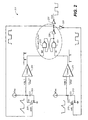
- FIG 2 is a block diagram of an exemplary embodiment for the relaxation oscillator 111, although, as with Figure 1 , other embodiments can be used.
- the output clock CLK is generated by charging and discharging of the two capacitors C0 203 and C1 213, with two comparators Comp 0 201 and Comp 1 211 and a SR latch, formed of cross-coupled NAND gates 221 and 223 and inverter 225.
- the comparator Comp0 201 sets the RS latch but the signal set to the input of the NAND gate 223, as shown by the waveform at the output of Comp0 201.
- the output of the latch (after inversion by 231) is the clock signal CLK with the waveform as shown.
- the signal CLK then travels (through the inverter 229, where the waveform at the output is shown) is applied to the gate of transistor T1 215 to initiate a charging operation for the other capacitor C 1 213.
- the output of the latch (the inverted CLK signal) is also applied to the gate of transistor T0 205 and discharges the capacitor C0 203.
- the comparator Comp1 211 When the voltage vcap2 across the second capacitor C1 213 , whose waveform is shown, reaches to the reference level, the comparator Comp1 211 resets the RS Latch. In this way, the output of the latch initiates the charging operation for the capacitor C0 203 and discharges the capacitor C1 213. This results in the continuous clock signal CLK being generated at the output of the latch.
- the clock frequency consequently depends on the charging current IOsc and the capacitor value C of C1 203 and C2 213.
- Figure 3 illustrates this frequency variation with process corners and DAC control bits of the relaxation oscillator.
- the vertical axis is the clock frequency and the horizontal axis is the 7-bit input value for Strim ⁇ 6:0>, with the actual behavior for an oscillator shown.
- the behavior of an oscillator for the nominal process values (a typical process corner, TT_27) is shown by the line 301.
- the DAC programming bit varies over the 7-bit input value, the frequency ranges from around 90MHz to around 320MHz.
- the line 303 shows the frequency versus programming bits behavior for a pair of fast process corners (FF_-40, FF_125), and line 305 shows the frequency versus programming bits behavior for a pair of slow process corners (SS_-40, SS_125).
- the Strim value for the nominal device is 79. This is shown in Table 1 on Figure 3 , where the frequency corresponding to bit 79 is shown for the illustrated process corners. For the slow corners, this is over 40MHz less than the desired 250MHz. For the fast corners, the frequency can be over 50MHz too high. Conversely, Table 2 shows the bit value needed to provide the desired 250MHz across the shown process variations. It is this Strim value that needs to be calibrated. To accommodate this frequency variation the current Iosc used to charge and discharge the relaxation oscillator's capacitors C0 203 and C1 213 shown in Figure2 is generated using IDAC 101 shown in Figure1 .
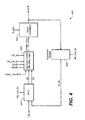
- Figure 4 is a block diagram of an exemplary embodiment of a relaxation oscillator calibration circuit 400 incorporating a phase-frequency detector (PFD) and min-max logic.
- the PFD and min-max logic can standard implementations, or other only-frequency detector blocks can be used in place of a PFD.
- the relaxation oscillation clock source Oscillator 100 can be that such as described above with respect Figures 1 and 2 .
- the inputs are the system enable signal SysEn, corresponding to the clock enable signal Clk_En of Figure 1 , and the trim value Strim ⁇ 6:0>.
- the other elements of Figure 4 are used to calibrate the value of Strim ⁇ 6:0>.
- the value of Strim is determined in the up-down counter/min-max logic 405.
- the circuit 405 receives an initial/default trim value (Initial_Trim ⁇ 6:0>) and, based on the UP and DN inputs, raises or lowers the trim value.
- the circuit 405 also receives a reference clock (Clk-ref), the system enable signal (SysEn), a clock calibration enable signal (Clk_Cal_En), and a module enable signal (ModEn). These various signal are used to adjust the trim value during calibration as described below.
- the trim adjust values UP and DN which are used to alter the trim value a bit at a time, are supplied from the frequency phase detector PFD 407, whose inputs are the reference clock value (Clk_ref) and calibration enable signal (Clk_Cal_En), as well as the feed-back clock signal from Clk.
- the PFD 407 is used to compare the value CLK against a reference value, but as the desired frequency of Clk may differ from the reference value (Clk_ref), a feedback divider circuit 403 can be included to receive the clock signal Clk from Oscillator 100 and, when enabled by (Clk_Cal_En), provides the suitably clock frequency fb_clk to PFD 407.
- the calibration process can be performed before shipping of the device, at test time for example, beginning with the default control bits Initial_Trim ⁇ 6:0> corresponding to the nominal process corner TT_27 are transferred to the corresponding node and the oscillator in the clock block 100 generates the output frequency which depends upon the manufactured silicon corner and could be higher or lower than the desired nominal value.
- the control signal Clk_Cal_En is enabled (made high)
- the phase-frequency detector (PFD) 407 starts comparing the tester reference clock Clk_ref (a JTAG test clock, for example) with the divided output clock fb_clk. If this divided output clock is higher than the tester reference clock, a down DN pulse gets generated and the control bits of the DAC is reduced by one bit (LSB).
- this loop is not a complete phase locked loop (PLL) and the output frequency of the clock block 100 is only function of the control bits Strim ⁇ 6:0>, without any phase co-relation to the tester reference clock, after certain time (when output frequency come in right range) the output frequency may start varying in a triangular fashion, as the Clk value goes between overshooting and undershooting the desired value as the circuit iterates through cycle of generating the clock signal, comparing the frequency, and adjusting the trim value.
- the range of this triangular frequency variation depends upon the sensitivity of the PFD and is due to a few other factors.
- a first factor is that the exemplary embodiment of Figure 4 is using a phase-frequency detector PFD 407, which tries to change the trim bit or control bits of Strm such that output frequency comes close to desired value.
- the PFD 407 start adjusting the phase of the two input frequencies, means it tries to increase/decrease the frequency such that the phases are also aligned.
- the outputs UP and DN of PFD 407 will keep giving high or low pulses as it tries to increase and decrease frequency as phases are not aligned. Due to this alignment of phase issue the output frequency will tend to overcorrect.
- the system is to be calibrated to a frequency of 256MHz, which, with a frequency divider ratio of 256, allows it to be compared to a reference frequency of 1MHz.
- the system enable signal (SysEn) is taken high, as shown in the third trace in Figure 5 , and the oscillator provides a clock signal whose frequency is determined by the Initial_Trim value. In this case, this corresponds to about 301MHz, as shown in the top trace of Figure 5 .
- the clock calibration enable signal Clk_Cal_En goes high, as shown in the second trace of Figure 5 and, as the clock frequency is above the expected frequency, the trim value begins to count down and the clock frequency (top trace) is correspondingly lowered toward the desired frequency. As described, however, the system will overshoot (or, rather, undershoot) the expected frequency by some distance before it reverses itself, begins to increase and overshoot on the high side. This over correction continues on, leading to the triangular waveform described above.
- the "ModEn” signal (bottom trace in Figure 5 ) is enabled (made “HIGH”).
- the Min-Max logic of block 405 finds the DAC controls bits corresponding to the maximum and minimum frequencies in the triangular frequency variation and, when this "ModEn” signal subsequently goes “Low” this logic locks the average controls bits at the "STrim ⁇ 6:0>” node, which corresponds to the desired frequency output of the clock's block. These bits can be read by the tester and programmed for the particular die or could be stored in memory of the chip or could be written on E-fuse.
- the process should not start until the calibration has gone on long enough to establish the triangular behavior and continue long enough for at least one minimum and maximum.
- this method is significantly faster than the prior art techniques, it is possible to wait the equivalent of several minimum and maximum peaks before taking ModEn high and then allow it to stay high for several cycles.
- the values can be set by considering several typical devices and then allowing relatively generous timing margins, with the enable, disable points for ModEn can be set based on time or the number of iterations of adjusting the trim value.
- an exemplary device (corresponding to the values of Figure 3 ) can complete the full calibration cycle in ⁇ 300 mircoseconds, which is significantly lower than the ⁇ 1.7 second calibration time using the typical prior art arrangement. Also, there is no need of any costly output frequency measurement system.
- the Clk_Cal_En signal can be generated after a certain amount of delay from the SysEn; and this delay between SysEn and Clk_Cal_En should be more than the settling time of oscillator.
- the Clk_Cal_En signal can also be independently controlled by firmware, controlling the test function or calibration process.
- the typical settling time of the oscillator is ⁇ 500nS.
- the "ModEn" signal is being generated internally after certain delay from the Clk_Cal_En and this delay time can be predefined during design phase.
- the circuit will generally be a part of larger circuit on a chip that is formed as part of a wafer that is expected to be manufactured according to the typical process corner.
- the typical process corner is where the various devices on the chip are manufactured to have the typical, or nominal, value prescribed for the device and corresponds to the "TT_27" device of line 301 in Figure 3 .
- Due to process variations, in practice the wafers may be in the slow (SS) or fast (FF) process comers; it is also not unusual for that a wafer or a particular silicon chip is not completely in a particular, say FF, corner but only partially so. It is these process variations for which the above described techniques determine and compensate. Before leaving the subject, these variations are considered further.
- the output frequency is ⁇ 300MHz for initial Strim bit setting of 79, where as the desired frequency in this example is 250MHz. It is also possible that a similar clock circuit formed elsewhere on the same wafer is also in a less fast, but faster than typical corner that provides a frequency of, say, 270MHz or some other number in between 250MHz to ⁇ 300MHz. (Similar variations can also occur for slow (SS) corner devices.) During the calibration process as described above, for a fast corner the control bits of Strim will step down and will eventually be set to provide the desired frequency of 250MHz.
- FF fast
- SS slow
- a second, important, piece of information that be concluded is how much fast (FF) or how slow (SS) the chip is: For example, for a 250MHz clock frequency, by referring to Table 2 of Figure 3 , it can be seen that if the Strim value is moved from bit 79 to 54, then the chip was in a complete FF comer; but if the calibration only changes the Strim value from the initial 79 to 67, then chip was only ⁇ 50% fast with respect to the "full" TT corner. This additional piece of information can be extracted from this calibration process. This additional information, which is a byproduct of the relaxation oscillator calibration process, can then be used to fine tune different parts of the chip, such as reference voltages, currents or other important process-dependent device parameters.
- FF fast
- SS slow
Landscapes
- Engineering & Computer Science (AREA)
- Power Engineering (AREA)
- Stabilization Of Oscillater, Synchronisation, Frequency Synthesizers (AREA)
Claims (12)
- Schaltung, Folgendes umfassend:eine Takterzeugungsschaltung (100) einschließlich eines Oszillators, der ein kalibrierbares Ausgangstaktsignal (CLK) mit einer Frequenz erzeugt, die von einem Trimwert abhängt;eine Frequenzvergleichsschaltung (407), die angeschlossen ist, um ein Referenztaktsignal (Clk_ref) und ein Feedback-Taktsignal (fb_clk) zu empfangen, die vom kalibrierbaren Ausgangstaktsignal (CLK) abgeleitet sind, und eine Anzeige darüber bereitzustellen, ob das Feedback-Taktsignal (fb_clk) eine Frequenz hat, die höher oder niedriger ist als eine Frequenz des Referenztaktsignals (Clk_ref); undeine Trimwert-Anpassungsschaltung (405), Folgendes einschließend:einen Up-Down-Zähler, der angeschlossen ist, um die Anzeige zu empfangen und als Reaktion darauf den Trimwert nach oben oder nach unten anzupassen, wobei mit einem Anfangs/Default-Trimwert angefangen wird;dadurch gekennzeichnet, dass:der Oszillator ein Relaxationsoszillator (111) ist; unddie Trimwert-Anpassungsschaltung (405) außerdem einschließt:Minimax-Logik zum Bestimmen des Minimums und Maximums der Trimwerte als Reaktion auf die Assertion eines Freigabesignals (ModEn) und zum Setzen des Trimwerts auf einen vom Minimum und Maximum der Trimwerte abgeleiteten Wert als Reaktion auf die Deassertion des Freigabesignals (ModEn).
- Schaltung nach Anspruch 1, worin die Takterzeugungsschaltung (100) außerdem einschließt:eine Stromquelle (101), die angeschlossen ist, um den Trimwert zu empfangen, einen Stromwert (IOsc) zu erzeugen, der vom Trimwert abhängt, und dem Relaxationsoszillator (111) den Stromwert (IOsc) zuzuführen.
- Schaltung nach Anspruch 2, worin die Takterzeugungsschaltung (100) außerdem einschließt:eine Spannungsregulierschaltung (105), die angeschlossen ist, um dem Relaxationsoszillator (111) eine Spannungsversorgung (Vdd_loc) bereitzustellen; undeine Referenzerzeugungsschaltung (103), die angeschlossen ist, um der Spannungsregulierschaltung (105) und der Relaxationsoszillatorschaltung (111) Referenzspannungen (Vref1, Vref2) zuzuführen.
- Schaltung nach Anspruch 2, wobei der Relaxationsoszillator (111) einen ersten Kondensator (210) und einen zweiten Kondensator (202) einschließt, deren jeder angeschlossen ist, um den Strom (IOsc) von der Stromquelle (101) zu empfangen.
- Schaltung nach Anspruch 1, außerdem umfassend:einen Frequenzteiler (403), der angeschlossen ist, um das kalibrierbare Ausgangstaktsignal (CLK) zu empfangen und daraus das geteilte Feedback-Taktsignal (fb_clk) zu erzeugen.
- Schaltung nach Anspruch 1, worin das Referenztaktsignal (Clk_ref) extern zugeführt wird.
- Verfahren zum Kalibrieren der Frequenz einer Taktschaltung (100), die ein Taktsignal (Clk) von einem Oszillator erzeugt, Folgendes umfassend:Empfangen eines Anfangs-Trimwerts; iteratives Ausführen eines Prozesses, Folgendes einschließend:Erzeugen eines Taktsignals (Clk) durch den Oszillator mit einer Frequenz, die vom Trimwert abhängt;Ausführen eines Vergleichs der Frequenz des Taktsignals (Clk) mit einem Referenz-Taktfrequenzwert (Clk_ref); undAnpassen des Trimwerts durch einen Up-Down-Zähler auf der Basis des Vergleichs;dadurch gekennzeichnet, dass:der Oszillator ein Relaxationsoszillator (111) ist und das Verfahren außerdem umfasst:nach Ausführen des Prozesses über mehrfache Iterationen während dessen Verlaufs, das Maximum und das Minimum des Trimwerts bestimmen; undEinstellen des End-Trimwerts auf der Basis des Maximum- und Minimum-Trimwerts.
- Verfahren nach Anspruch 7, außerdem umfassend:Empfangen des Trimwerts an einer Stromquelle (101);in der Stromquelle (101) einen Stromwert (IOcs) erzeugen, der vom Trimwert abhängt; undZuführen des Stromwerts (IOsc) an den Relaxationsoszillator (111).
- Verfahren nach Anspruch 8, außerdem umfassend;
Bereitstellen einer Spannungsversorgung (Vdd_loc) an den Relaxationsoszillator (111) von einer Spannungsregulierschaltung (105); und
Zuführen von Referenzspannungen (Vref1, Vref2) von einer Referenzerzeugungsschaltung (103) an die Spannungsregulierschaltung (105) und die Relaxationsoszillatorschaltung (111). - Verfahren nach Anspruch 8, worin der Relaxationsoszillator (111) einen ersten Kondensator (201) und einen zweiten Kondensator (202) einschließt, das Verfahren außerdem umfassend:Empfangen des Stroms (IOsc) von der Stromquelle (101) an dem ersten (201) und zweiten (202) Kondensator.
- Verfahren nach Anspruch 7, außerdem umfassend:Empfangen des Taktsignals (Clk) an einem Frequenzteiler (403); undErzeugen eines geteilten Feedback-Taktsignals (fb_clk) aus dem Taktsignal (Clk) auf dem Frequenzteiler (403), worin der Vergleich der Frequenz des Taktsignals (Clk) mit einem Referenz-Taktfrequenzwert (Clk_ref) das geteilte Feedback-Taktsignal (fb_clk) mit der Referenztaktfrequenz (Clk_ref) vergleicht.
- Verfahren nach Anspruch 7, worin das Referenztaktsignal (Clk_ref) extern zugeführt wird.
Applications Claiming Priority (2)
| Application Number | Priority Date | Filing Date | Title |
|---|---|---|---|
| US12/754,836 US8085099B2 (en) | 2010-04-06 | 2010-04-06 | Self-calibrating relaxation oscillator based clock source |
| PCT/US2011/030556 WO2011126896A1 (en) | 2010-04-06 | 2011-03-30 | Calibrated relaxation oscillator using a pll |
Publications (2)
| Publication Number | Publication Date |
|---|---|
| EP2556592A1 EP2556592A1 (de) | 2013-02-13 |
| EP2556592B1 true EP2556592B1 (de) | 2014-03-19 |
Family
ID=44021878
Family Applications (1)
| Application Number | Title | Priority Date | Filing Date |
|---|---|---|---|
| EP11713942.8A Not-in-force EP2556592B1 (de) | 2010-04-06 | 2011-03-30 | Kalibrierter kipposzillator mit einem phasenregelkreis |
Country Status (7)
| Country | Link |
|---|---|
| US (2) | US8085099B2 (de) |
| EP (1) | EP2556592B1 (de) |
| JP (1) | JP5581507B2 (de) |
| KR (1) | KR101632467B1 (de) |
| CN (1) | CN102934363B (de) |
| TW (1) | TWI467921B (de) |
| WO (1) | WO2011126896A1 (de) |
Families Citing this family (26)
| Publication number | Priority date | Publication date | Assignee | Title |
|---|---|---|---|---|
| US8085099B2 (en) | 2010-04-06 | 2011-12-27 | Sandisk Technologies Inc. | Self-calibrating relaxation oscillator based clock source |
| US8502609B2 (en) | 2011-06-10 | 2013-08-06 | Broadcom Corporation | Reference-less frequency detector |
| US9281828B2 (en) * | 2011-06-10 | 2016-03-08 | Broadcom Corporation | Reference-less voltage controlled oscillator (VCO) calibration |
| US20130223152A1 (en) * | 2011-08-02 | 2013-08-29 | Elpida Memory, Inc. | Clock generator |
| JP2013038744A (ja) * | 2011-08-11 | 2013-02-21 | Renesas Electronics Corp | 発振回路及びそれを備えた半導体集積回路 |
| KR101876997B1 (ko) * | 2012-01-19 | 2018-07-10 | 삼성전자 주식회사 | 오실레이터 오토 트리밍 방법 및 오실레이터 오토 트리밍 기능을 갖는 반도체 장치 |
| US8805505B1 (en) | 2013-01-25 | 2014-08-12 | Medtronic, Inc. | Using telemetry downlink for real time clock calibration |
| US9484940B2 (en) | 2013-01-25 | 2016-11-01 | Medtronic, Inc. | Using high frequency crystal from external module to trim real time clock |
| US9093336B2 (en) | 2013-02-12 | 2015-07-28 | Texas Instruments Incorporated | Determining optimum code from default, programmable, and test trim codes |
| CN103391045B (zh) * | 2013-07-30 | 2015-11-25 | 浙江大学 | 抗工艺涨落的自修调集成电路片上振荡器 |
| JP6153828B2 (ja) * | 2013-09-10 | 2017-06-28 | 日立オートモティブシステムズ株式会社 | 発振回路、それを用いた半導体集積回路装置および回転角検出装置 |
| DE102013111062B4 (de) * | 2013-10-07 | 2017-03-16 | Borgwarner Ludwigsburg Gmbh | Verfahren zum Einstellen einer Anregungsfrequenz eines Schwingkreises einer Koronazündeinrichtung |
| US9514831B2 (en) | 2014-01-29 | 2016-12-06 | Sandisk Technologies Llc | Multi-clock generation through phase locked loop (PLL) reference |
| US9325276B2 (en) | 2014-03-03 | 2016-04-26 | Sandisk Technologies Inc. | Methods and apparatus for clock oscillator temperature coefficient trimming |
| KR101593784B1 (ko) * | 2014-03-14 | 2016-02-29 | 성균관대학교산학협력단 | 이장 발진기를 이용한 확산 스펙트럼 클럭 생성 장치 및 방법 |
| DE102014014449A1 (de) * | 2014-09-26 | 2016-03-31 | Giesecke & Devrient Gmbh | Verfahren und Sicherheitsmodul zum Empfang von zwei Signalen |
| US9876979B1 (en) * | 2016-12-06 | 2018-01-23 | Omnivision Technologies, Inc. | Current generator |
| US10157087B1 (en) * | 2017-07-14 | 2018-12-18 | Nxp Usa, Inc. | Robust boot block design and architecture |
| TWI675280B (zh) * | 2018-10-25 | 2019-10-21 | 新唐科技股份有限公司 | 時脈產生電路及其時脈調整方法 |
| US10782727B2 (en) * | 2018-11-19 | 2020-09-22 | Texas Instruments Incorporated | Integrated circuits having self-calibrating oscillators, and methods of operating the same |
| CN112269424A (zh) * | 2020-11-19 | 2021-01-26 | 珠海零边界集成电路有限公司 | 一种芯片时钟频率校准方法、装置、设备和介质 |
| KR102925794B1 (ko) | 2021-06-17 | 2026-02-09 | 삼성전자 주식회사 | 오실레이터 클럭 신호의 주기를 조정하는 클럭 생성 회로 및 그 방법 |
| CN114696824B (zh) * | 2022-06-01 | 2022-09-20 | 浙江地芯引力科技有限公司 | 全差分模数转换器及电容权重校准方法和装置 |
| CN115276607B (zh) * | 2022-07-15 | 2025-10-10 | 成都爱旗科技有限公司 | 一种时钟校准结构及其校准方法 |
| CN118300532B (zh) * | 2023-01-04 | 2025-04-11 | 湖南芯力特电子科技有限公司 | 低功耗振荡器电路及电子设备 |
| CN121356537B (zh) * | 2025-12-16 | 2026-03-17 | 湖南进芯电子科技有限公司 | 自修调方法、装置、设备及存储介质 |
Family Cites Families (32)
| Publication number | Priority date | Publication date | Assignee | Title |
|---|---|---|---|---|
| US5887145A (en) | 1993-09-01 | 1999-03-23 | Sandisk Corporation | Removable mother/daughter peripheral card |
| FR2726921B1 (fr) * | 1994-11-16 | 1997-04-25 | Ela Medical Sa | Procede d'ajustage d'un parametre electrique d'un dispositif electronique, notamment d'un stimulateur ou d'un defibrillateur cardiaque, et dispositif le mettant en oeuvre |
| JPH08190587A (ja) | 1995-01-06 | 1996-07-23 | Hitachi Ltd | 業務プロセスのシミュレーションシステム |
| US5687202A (en) * | 1995-04-24 | 1997-11-11 | Cyrix Corporation | Programmable phase shift clock generator |
| US5699024A (en) | 1996-05-06 | 1997-12-16 | Delco Electronics Corporation | Accurate integrated oscillator circuit |
| EP0841754A3 (de) * | 1996-11-08 | 1998-12-16 | Texas Instruments Incorporated | Digital gesteuerter Oszillator |
| US6028905A (en) * | 1997-08-28 | 2000-02-22 | Ericsson Inc. | Charge pump steering systems and methods for loop filters of phase locked loops |
| US5942949A (en) | 1997-10-14 | 1999-08-24 | Lucent Technologies Inc. | Self-calibrating phase-lock loop with auto-trim operations for selecting an appropriate oscillator operating curve |
| US6356161B1 (en) * | 1998-03-19 | 2002-03-12 | Microchip Technology Inc. | Calibration techniques for a precision relaxation oscillator integrated circuit with temperature compensation |
| US6040622A (en) | 1998-06-11 | 2000-03-21 | Sandisk Corporation | Semiconductor package using terminals formed on a conductive layer of a circuit board |
| US6901457B1 (en) | 1998-11-04 | 2005-05-31 | Sandisk Corporation | Multiple mode communications system |
| US6279114B1 (en) | 1998-11-04 | 2001-08-21 | Sandisk Corporation | Voltage negotiation in a single host multiple cards system |
| US6124764A (en) * | 1999-01-22 | 2000-09-26 | Telefonaktiebolaget Lm Ericsson | Stable low-power oscillator |
| JP2001211070A (ja) * | 2000-01-26 | 2001-08-03 | Kawasaki Steel Corp | Pll回路 |
| JP2001332969A (ja) * | 2000-05-23 | 2001-11-30 | Nec Microsystems Ltd | 発振装置 |
| US6824063B1 (en) | 2000-08-04 | 2004-11-30 | Sandisk Corporation | Use of small electronic circuit cards with different interfaces in an electronic system |
| US6820148B1 (en) | 2000-08-17 | 2004-11-16 | Sandisk Corporation | Multiple removable non-volatile memory cards serially communicating with a host |
| US6798299B1 (en) | 2000-10-26 | 2004-09-28 | Cypress Semiconductor Corporation | Crystal-less oscillator circuit with trimmable analog current control for increased stability |
| US20040064612A1 (en) | 2002-09-26 | 2004-04-01 | Sandisk Corporation | Method and system for using a memory card protocol inside a bus protocol |
| US6727768B1 (en) * | 2002-10-29 | 2004-04-27 | Institute Of Microelectronics | Relaxation CCO for PLL-based constant tuning of GM-C filters |
| DE10308643A1 (de) | 2003-02-27 | 2004-09-16 | Infineon Technologies Ag | Phasenregelanordnung |
| US7305535B2 (en) | 2003-04-17 | 2007-12-04 | Sandisk Corporation | Memory cards including a standard security function |
| US7370168B2 (en) | 2003-04-25 | 2008-05-06 | Renesas Technology Corp. | Memory card conforming to a multiple operation standards |
| US7152801B2 (en) | 2004-04-16 | 2006-12-26 | Sandisk Corporation | Memory cards having two standard sets of contacts |
| US7432749B1 (en) * | 2004-06-23 | 2008-10-07 | Cypress Semiconductor Corp. | Circuit and method for improving frequency range in a phase locked loop |
| US7746181B1 (en) * | 2005-01-28 | 2010-06-29 | Cypress Semiconductor Corporation | Circuit and method for extending the usable frequency range of a phase locked loop (PLL) |
| KR100849065B1 (ko) | 2005-12-15 | 2008-07-30 | 주식회사 하이닉스반도체 | 동기식 메모리 장치의 드라이버 및 오디티 임피던스 조절방법 |
| US8228126B2 (en) * | 2007-04-19 | 2012-07-24 | Mediatek Inc. | Multi-band burst-mode clock and data recovery circuit |
| CN100562021C (zh) | 2007-07-10 | 2009-11-18 | 北京易路联动技术有限公司 | 一种分布式可同步的多源数据的控制方法和装置 |
| US8073092B2 (en) | 2008-06-19 | 2011-12-06 | Microchip Technology Incorporated | Automatic synchronization of an internal oscillator to an external frequency reference |
| TWM349634U (en) * | 2008-09-10 | 2009-01-21 | Amazing Microelectronic Corp | Programmable voltage-controlled oscillator |
| US8085099B2 (en) | 2010-04-06 | 2011-12-27 | Sandisk Technologies Inc. | Self-calibrating relaxation oscillator based clock source |
-
2010
- 2010-04-06 US US12/754,836 patent/US8085099B2/en not_active Expired - Fee Related
-
2011
- 2011-03-30 EP EP11713942.8A patent/EP2556592B1/de not_active Not-in-force
- 2011-03-30 JP JP2013503792A patent/JP5581507B2/ja not_active Expired - Fee Related
- 2011-03-30 CN CN201180027956.5A patent/CN102934363B/zh not_active Expired - Fee Related
- 2011-03-30 KR KR1020127026107A patent/KR101632467B1/ko not_active Expired - Fee Related
- 2011-03-30 WO PCT/US2011/030556 patent/WO2011126896A1/en not_active Ceased
- 2011-04-06 TW TW100111876A patent/TWI467921B/zh not_active IP Right Cessation
- 2011-11-21 US US13/300,808 patent/US8669817B2/en not_active Expired - Fee Related
Also Published As
| Publication number | Publication date |
|---|---|
| JP5581507B2 (ja) | 2014-09-03 |
| WO2011126896A1 (en) | 2011-10-13 |
| TW201233066A (en) | 2012-08-01 |
| US20110241784A1 (en) | 2011-10-06 |
| EP2556592A1 (de) | 2013-02-13 |
| US20120062326A1 (en) | 2012-03-15 |
| US8085099B2 (en) | 2011-12-27 |
| CN102934363A (zh) | 2013-02-13 |
| US8669817B2 (en) | 2014-03-11 |
| TWI467921B (zh) | 2015-01-01 |
| CN102934363B (zh) | 2016-08-24 |
| KR101632467B1 (ko) | 2016-07-01 |
| KR20130065636A (ko) | 2013-06-19 |
| JP2013528981A (ja) | 2013-07-11 |
Similar Documents
| Publication | Publication Date | Title |
|---|---|---|
| US8085099B2 (en) | Self-calibrating relaxation oscillator based clock source | |
| CN103199857B (zh) | 基于电流控制振荡器(cco)的pll | |
| US8659362B2 (en) | Relaxation oscillator circuit with reduced sensitivity of oscillation frequency to comparator delay variation | |
| US7548100B2 (en) | Delay locked loop | |
| US8497741B2 (en) | High accuracy RC oscillator | |
| US6404246B1 (en) | Precision clock synthesizer using RC oscillator and calibration circuit | |
| US8570113B2 (en) | Digital VCO calibration method and apparatus | |
| US11418204B2 (en) | Phase lock loop (PLL) with operating parameter calibration circuit and method | |
| CN112292815B (zh) | 补偿晶体振荡器的频率变化以及相关系统、方法和设备 | |
| US7920000B2 (en) | PLL circuit and method of controlling the same | |
| US8278986B2 (en) | Trimming of a pseudo-closed loop programmable delay line | |
| CN102870329B (zh) | 具有内部rc振荡器的集成电路及用于校准rc振荡器的方法 | |
| WO2019126274A1 (en) | Apparatuses and methods for providing frequency divided clocks | |
| US20160182060A1 (en) | Duty cycle detection circuit and semiconductor apparatus including the same | |
| US20220345137A1 (en) | Phase locked loop generating adaptive driving voltage and related operating method | |
| KR101390393B1 (ko) | 전하 펌프의 전류 특성을 조정하는 전하 펌프 바이어스 조정 장치 및 이를 이용한 주파수 발생 장치 | |
| WO2023173041A1 (en) | Supply voltage based, or temperature based, fine control of a tunable oscillator of a pll | |
| US10224941B2 (en) | Oscillation apparatus and oscillation frequency adjustment method | |
| WO2025227163A1 (en) | Managing variation in phase-locked loop (pll) bandwidth, and related methods and apparatuses | |
| US7982553B2 (en) | Clock generator | |
| JP5444917B2 (ja) | 抵抗値調整回路 | |
| US7675367B2 (en) | Design structure for an automated real-time frequency band selection circuit for use with a voltage controlled oscillator | |
| US7642824B2 (en) | PLL circuit and method of controlling the same | |
| KR20080024896A (ko) | 전압 제어 발진기의 이득 측정 방법 및 이를 이용하는주파수 합성기 |
Legal Events
| Date | Code | Title | Description |
|---|---|---|---|
| PUAI | Public reference made under article 153(3) epc to a published international application that has entered the european phase |
Free format text: ORIGINAL CODE: 0009012 |
|
| 17P | Request for examination filed |
Effective date: 20120925 |
|
| AK | Designated contracting states |
Kind code of ref document: A1 Designated state(s): AL AT BE BG CH CY CZ DE DK EE ES FI FR GB GR HR HU IE IS IT LI LT LU LV MC MK MT NL NO PL PT RO RS SE SI SK SM TR |
|
| DAX | Request for extension of the european patent (deleted) | ||
| GRAP | Despatch of communication of intention to grant a patent |
Free format text: ORIGINAL CODE: EPIDOSNIGR1 |
|
| INTG | Intention to grant announced |
Effective date: 20130923 |
|
| GRAS | Grant fee paid |
Free format text: ORIGINAL CODE: EPIDOSNIGR3 |
|
| GRAA | (expected) grant |
Free format text: ORIGINAL CODE: 0009210 |
|
| AK | Designated contracting states |
Kind code of ref document: B1 Designated state(s): AL AT BE BG CH CY CZ DE DK EE ES FI FR GB GR HR HU IE IS IT LI LT LU LV MC MK MT NL NO PL PT RO RS SE SI SK SM TR |
|
| REG | Reference to a national code |
Ref country code: GB Ref legal event code: FG4D |
|
| REG | Reference to a national code |
Ref country code: CH Ref legal event code: EP |
|
| REG | Reference to a national code |
Ref country code: AT Ref legal event code: REF Ref document number: 658258 Country of ref document: AT Kind code of ref document: T Effective date: 20140415 |
|
| REG | Reference to a national code |
Ref country code: IE Ref legal event code: FG4D |
|
| REG | Reference to a national code |
Ref country code: DE Ref legal event code: R096 Ref document number: 602011005560 Country of ref document: DE Effective date: 20140430 |
|
| REG | Reference to a national code |
Ref country code: NL Ref legal event code: T3 |
|
| PG25 | Lapsed in a contracting state [announced via postgrant information from national office to epo] |
Ref country code: NO Free format text: LAPSE BECAUSE OF FAILURE TO SUBMIT A TRANSLATION OF THE DESCRIPTION OR TO PAY THE FEE WITHIN THE PRESCRIBED TIME-LIMIT Effective date: 20140619 Ref country code: LT Free format text: LAPSE BECAUSE OF FAILURE TO SUBMIT A TRANSLATION OF THE DESCRIPTION OR TO PAY THE FEE WITHIN THE PRESCRIBED TIME-LIMIT Effective date: 20140319 |
|
| REG | Reference to a national code |
Ref country code: AT Ref legal event code: MK05 Ref document number: 658258 Country of ref document: AT Kind code of ref document: T Effective date: 20140319 |
|
| REG | Reference to a national code |
Ref country code: LT Ref legal event code: MG4D |
|
| PG25 | Lapsed in a contracting state [announced via postgrant information from national office to epo] |
Ref country code: FI Free format text: LAPSE BECAUSE OF FAILURE TO SUBMIT A TRANSLATION OF THE DESCRIPTION OR TO PAY THE FEE WITHIN THE PRESCRIBED TIME-LIMIT Effective date: 20140319 Ref country code: CY Free format text: LAPSE BECAUSE OF FAILURE TO SUBMIT A TRANSLATION OF THE DESCRIPTION OR TO PAY THE FEE WITHIN THE PRESCRIBED TIME-LIMIT Effective date: 20140319 Ref country code: SE Free format text: LAPSE BECAUSE OF FAILURE TO SUBMIT A TRANSLATION OF THE DESCRIPTION OR TO PAY THE FEE WITHIN THE PRESCRIBED TIME-LIMIT Effective date: 20140319 |
|
| PG25 | Lapsed in a contracting state [announced via postgrant information from national office to epo] |
Ref country code: RS Free format text: LAPSE BECAUSE OF FAILURE TO SUBMIT A TRANSLATION OF THE DESCRIPTION OR TO PAY THE FEE WITHIN THE PRESCRIBED TIME-LIMIT Effective date: 20140319 Ref country code: LV Free format text: LAPSE BECAUSE OF FAILURE TO SUBMIT A TRANSLATION OF THE DESCRIPTION OR TO PAY THE FEE WITHIN THE PRESCRIBED TIME-LIMIT Effective date: 20140319 Ref country code: HR Free format text: LAPSE BECAUSE OF FAILURE TO SUBMIT A TRANSLATION OF THE DESCRIPTION OR TO PAY THE FEE WITHIN THE PRESCRIBED TIME-LIMIT Effective date: 20140319 |
|
| PG25 | Lapsed in a contracting state [announced via postgrant information from national office to epo] |
Ref country code: BG Free format text: LAPSE BECAUSE OF FAILURE TO SUBMIT A TRANSLATION OF THE DESCRIPTION OR TO PAY THE FEE WITHIN THE PRESCRIBED TIME-LIMIT Effective date: 20140619 Ref country code: BE Free format text: LAPSE BECAUSE OF FAILURE TO SUBMIT A TRANSLATION OF THE DESCRIPTION OR TO PAY THE FEE WITHIN THE PRESCRIBED TIME-LIMIT Effective date: 20140319 Ref country code: IS Free format text: LAPSE BECAUSE OF FAILURE TO SUBMIT A TRANSLATION OF THE DESCRIPTION OR TO PAY THE FEE WITHIN THE PRESCRIBED TIME-LIMIT Effective date: 20140719 Ref country code: RO Free format text: LAPSE BECAUSE OF FAILURE TO SUBMIT A TRANSLATION OF THE DESCRIPTION OR TO PAY THE FEE WITHIN THE PRESCRIBED TIME-LIMIT Effective date: 20140319 Ref country code: EE Free format text: LAPSE BECAUSE OF FAILURE TO SUBMIT A TRANSLATION OF THE DESCRIPTION OR TO PAY THE FEE WITHIN THE PRESCRIBED TIME-LIMIT Effective date: 20140319 Ref country code: CZ Free format text: LAPSE BECAUSE OF FAILURE TO SUBMIT A TRANSLATION OF THE DESCRIPTION OR TO PAY THE FEE WITHIN THE PRESCRIBED TIME-LIMIT Effective date: 20140319 |
|
| REG | Reference to a national code |
Ref country code: CH Ref legal event code: PL |
|
| PG25 | Lapsed in a contracting state [announced via postgrant information from national office to epo] |
Ref country code: PL Free format text: LAPSE BECAUSE OF FAILURE TO SUBMIT A TRANSLATION OF THE DESCRIPTION OR TO PAY THE FEE WITHIN THE PRESCRIBED TIME-LIMIT Effective date: 20140319 Ref country code: AT Free format text: LAPSE BECAUSE OF FAILURE TO SUBMIT A TRANSLATION OF THE DESCRIPTION OR TO PAY THE FEE WITHIN THE PRESCRIBED TIME-LIMIT Effective date: 20140319 Ref country code: ES Free format text: LAPSE BECAUSE OF FAILURE TO SUBMIT A TRANSLATION OF THE DESCRIPTION OR TO PAY THE FEE WITHIN THE PRESCRIBED TIME-LIMIT Effective date: 20140319 Ref country code: SK Free format text: LAPSE BECAUSE OF FAILURE TO SUBMIT A TRANSLATION OF THE DESCRIPTION OR TO PAY THE FEE WITHIN THE PRESCRIBED TIME-LIMIT Effective date: 20140319 |
|
| REG | Reference to a national code |
Ref country code: DE Ref legal event code: R097 Ref document number: 602011005560 Country of ref document: DE |
|
| PG25 | Lapsed in a contracting state [announced via postgrant information from national office to epo] |
Ref country code: PT Free format text: LAPSE BECAUSE OF FAILURE TO SUBMIT A TRANSLATION OF THE DESCRIPTION OR TO PAY THE FEE WITHIN THE PRESCRIBED TIME-LIMIT Effective date: 20140721 |
|
| REG | Reference to a national code |
Ref country code: IE Ref legal event code: MM4A |
|
| PLBE | No opposition filed within time limit |
Free format text: ORIGINAL CODE: 0009261 |
|
| STAA | Information on the status of an ep patent application or granted ep patent |
Free format text: STATUS: NO OPPOSITION FILED WITHIN TIME LIMIT |
|
| PG25 | Lapsed in a contracting state [announced via postgrant information from national office to epo] |
Ref country code: MC Free format text: LAPSE BECAUSE OF FAILURE TO SUBMIT A TRANSLATION OF THE DESCRIPTION OR TO PAY THE FEE WITHIN THE PRESCRIBED TIME-LIMIT Effective date: 20140319 Ref country code: LI Free format text: LAPSE BECAUSE OF NON-PAYMENT OF DUE FEES Effective date: 20140331 Ref country code: CH Free format text: LAPSE BECAUSE OF NON-PAYMENT OF DUE FEES Effective date: 20140331 Ref country code: DK Free format text: LAPSE BECAUSE OF FAILURE TO SUBMIT A TRANSLATION OF THE DESCRIPTION OR TO PAY THE FEE WITHIN THE PRESCRIBED TIME-LIMIT Effective date: 20140319 Ref country code: IE Free format text: LAPSE BECAUSE OF NON-PAYMENT OF DUE FEES Effective date: 20140330 |
|
| 26N | No opposition filed |
Effective date: 20141222 |
|
| REG | Reference to a national code |
Ref country code: FR Ref legal event code: ST Effective date: 20150212 |
|
| PG25 | Lapsed in a contracting state [announced via postgrant information from national office to epo] |
Ref country code: IT Free format text: LAPSE BECAUSE OF FAILURE TO SUBMIT A TRANSLATION OF THE DESCRIPTION OR TO PAY THE FEE WITHIN THE PRESCRIBED TIME-LIMIT Effective date: 20140319 |
|
| REG | Reference to a national code |
Ref country code: DE Ref legal event code: R097 Ref document number: 602011005560 Country of ref document: DE Effective date: 20141222 |
|
| PG25 | Lapsed in a contracting state [announced via postgrant information from national office to epo] |
Ref country code: FR Free format text: LAPSE BECAUSE OF NON-PAYMENT OF DUE FEES Effective date: 20140519 |
|
| PG25 | Lapsed in a contracting state [announced via postgrant information from national office to epo] |
Ref country code: SI Free format text: LAPSE BECAUSE OF FAILURE TO SUBMIT A TRANSLATION OF THE DESCRIPTION OR TO PAY THE FEE WITHIN THE PRESCRIBED TIME-LIMIT Effective date: 20140319 |
|
| PG25 | Lapsed in a contracting state [announced via postgrant information from national office to epo] |
Ref country code: MT Free format text: LAPSE BECAUSE OF FAILURE TO SUBMIT A TRANSLATION OF THE DESCRIPTION OR TO PAY THE FEE WITHIN THE PRESCRIBED TIME-LIMIT Effective date: 20140319 |
|
| PG25 | Lapsed in a contracting state [announced via postgrant information from national office to epo] |
Ref country code: SM Free format text: LAPSE BECAUSE OF FAILURE TO SUBMIT A TRANSLATION OF THE DESCRIPTION OR TO PAY THE FEE WITHIN THE PRESCRIBED TIME-LIMIT Effective date: 20140319 |
|
| PG25 | Lapsed in a contracting state [announced via postgrant information from national office to epo] |
Ref country code: GR Free format text: LAPSE BECAUSE OF FAILURE TO SUBMIT A TRANSLATION OF THE DESCRIPTION OR TO PAY THE FEE WITHIN THE PRESCRIBED TIME-LIMIT Effective date: 20140620 |
|
| PG25 | Lapsed in a contracting state [announced via postgrant information from national office to epo] |
Ref country code: LU Free format text: LAPSE BECAUSE OF NON-PAYMENT OF DUE FEES Effective date: 20140330 Ref country code: TR Free format text: LAPSE BECAUSE OF FAILURE TO SUBMIT A TRANSLATION OF THE DESCRIPTION OR TO PAY THE FEE WITHIN THE PRESCRIBED TIME-LIMIT Effective date: 20140319 Ref country code: HU Free format text: LAPSE BECAUSE OF FAILURE TO SUBMIT A TRANSLATION OF THE DESCRIPTION OR TO PAY THE FEE WITHIN THE PRESCRIBED TIME-LIMIT; INVALID AB INITIO Effective date: 20110330 |
|
| REG | Reference to a national code |
Ref country code: DE Ref legal event code: R082 Ref document number: 602011005560 Country of ref document: DE Representative=s name: MARKS & CLERK (LUXEMBOURG) LLP, LU Ref country code: DE Ref legal event code: R081 Ref document number: 602011005560 Country of ref document: DE Owner name: SANDISK TECHNOLOGIES LLC, PLANO, US Free format text: FORMER OWNER: SANDISK TECHNOLOGIES INC., PLANO, TEX., US |
|
| PGFP | Annual fee paid to national office [announced via postgrant information from national office to epo] |
Ref country code: NL Payment date: 20180314 Year of fee payment: 8 Ref country code: GB Payment date: 20180329 Year of fee payment: 8 |
|
| PG25 | Lapsed in a contracting state [announced via postgrant information from national office to epo] |
Ref country code: MK Free format text: LAPSE BECAUSE OF FAILURE TO SUBMIT A TRANSLATION OF THE DESCRIPTION OR TO PAY THE FEE WITHIN THE PRESCRIBED TIME-LIMIT Effective date: 20140319 |
|
| PG25 | Lapsed in a contracting state [announced via postgrant information from national office to epo] |
Ref country code: AL Free format text: LAPSE BECAUSE OF FAILURE TO SUBMIT A TRANSLATION OF THE DESCRIPTION OR TO PAY THE FEE WITHIN THE PRESCRIBED TIME-LIMIT Effective date: 20140319 |
|
| PGFP | Annual fee paid to national office [announced via postgrant information from national office to epo] |
Ref country code: DE Payment date: 20190319 Year of fee payment: 9 |
|
| REG | Reference to a national code |
Ref country code: NL Ref legal event code: MM Effective date: 20190401 |
|
| GBPC | Gb: european patent ceased through non-payment of renewal fee |
Effective date: 20190330 |
|
| PG25 | Lapsed in a contracting state [announced via postgrant information from national office to epo] |
Ref country code: NL Free format text: LAPSE BECAUSE OF NON-PAYMENT OF DUE FEES Effective date: 20190401 Ref country code: GB Free format text: LAPSE BECAUSE OF NON-PAYMENT OF DUE FEES Effective date: 20190330 |
|
| REG | Reference to a national code |
Ref country code: DE Ref legal event code: R119 Ref document number: 602011005560 Country of ref document: DE |
|
| PG25 | Lapsed in a contracting state [announced via postgrant information from national office to epo] |
Ref country code: DE Free format text: LAPSE BECAUSE OF NON-PAYMENT OF DUE FEES Effective date: 20201001 |