EP2553798B1 - Alimentation à découpage pourvue d'un régulateur de tension - Google Patents
Alimentation à découpage pourvue d'un régulateur de tension Download PDFInfo
- Publication number
- EP2553798B1 EP2553798B1 EP10713162.5A EP10713162A EP2553798B1 EP 2553798 B1 EP2553798 B1 EP 2553798B1 EP 10713162 A EP10713162 A EP 10713162A EP 2553798 B1 EP2553798 B1 EP 2553798B1
- Authority
- EP
- European Patent Office
- Prior art keywords
- voltage regulator
- pulse
- power supply
- pulses
- primary side
- Prior art date
- Legal status (The legal status is an assumption and is not a legal conclusion. Google has not performed a legal analysis and makes no representation as to the accuracy of the status listed.)
- Active
Links
Images


Classifications
-
- H—ELECTRICITY
- H02—GENERATION; CONVERSION OR DISTRIBUTION OF ELECTRIC POWER
- H02M—APPARATUS FOR CONVERSION BETWEEN AC AND AC, BETWEEN AC AND DC, OR BETWEEN DC AND DC, AND FOR USE WITH MAINS OR SIMILAR POWER SUPPLY SYSTEMS; CONVERSION OF DC OR AC INPUT POWER INTO SURGE OUTPUT POWER; CONTROL OR REGULATION THEREOF
- H02M3/00—Conversion of dc power input into dc power output
- H02M3/22—Conversion of dc power input into dc power output with intermediate conversion into ac
- H02M3/24—Conversion of dc power input into dc power output with intermediate conversion into ac by static converters
- H02M3/28—Conversion of dc power input into dc power output with intermediate conversion into ac by static converters using discharge tubes with control electrode or semiconductor devices with control electrode to produce the intermediate ac
- H02M3/325—Conversion of dc power input into dc power output with intermediate conversion into ac by static converters using discharge tubes with control electrode or semiconductor devices with control electrode to produce the intermediate ac using devices of a triode or a transistor type requiring continuous application of a control signal
- H02M3/335—Conversion of dc power input into dc power output with intermediate conversion into ac by static converters using discharge tubes with control electrode or semiconductor devices with control electrode to produce the intermediate ac using devices of a triode or a transistor type requiring continuous application of a control signal using semiconductor devices only
- H02M3/33507—Conversion of dc power input into dc power output with intermediate conversion into ac by static converters using discharge tubes with control electrode or semiconductor devices with control electrode to produce the intermediate ac using devices of a triode or a transistor type requiring continuous application of a control signal using semiconductor devices only with automatic control of the output voltage or current, e.g. flyback converters
-
- H—ELECTRICITY
- H02—GENERATION; CONVERSION OR DISTRIBUTION OF ELECTRIC POWER
- H02M—APPARATUS FOR CONVERSION BETWEEN AC AND AC, BETWEEN AC AND DC, OR BETWEEN DC AND DC, AND FOR USE WITH MAINS OR SIMILAR POWER SUPPLY SYSTEMS; CONVERSION OF DC OR AC INPUT POWER INTO SURGE OUTPUT POWER; CONTROL OR REGULATION THEREOF
- H02M1/00—Details of apparatus for conversion
- H02M1/36—Means for starting or stopping converters
-
- H—ELECTRICITY
- H02—GENERATION; CONVERSION OR DISTRIBUTION OF ELECTRIC POWER
- H02M—APPARATUS FOR CONVERSION BETWEEN AC AND AC, BETWEEN AC AND DC, OR BETWEEN DC AND DC, AND FOR USE WITH MAINS OR SIMILAR POWER SUPPLY SYSTEMS; CONVERSION OF DC OR AC INPUT POWER INTO SURGE OUTPUT POWER; CONTROL OR REGULATION THEREOF
- H02M1/00—Details of apparatus for conversion
- H02M1/42—Circuits or arrangements for compensating for or adjusting power factor in converters or inverters
- H02M1/4208—Arrangements for improving power factor of AC input
- H02M1/4233—Arrangements for improving power factor of AC input using a bridge converter comprising active switches
-
- H—ELECTRICITY
- H02—GENERATION; CONVERSION OR DISTRIBUTION OF ELECTRIC POWER
- H02M—APPARATUS FOR CONVERSION BETWEEN AC AND AC, BETWEEN AC AND DC, OR BETWEEN DC AND DC, AND FOR USE WITH MAINS OR SIMILAR POWER SUPPLY SYSTEMS; CONVERSION OF DC OR AC INPUT POWER INTO SURGE OUTPUT POWER; CONTROL OR REGULATION THEREOF
- H02M3/00—Conversion of dc power input into dc power output
- H02M3/22—Conversion of dc power input into dc power output with intermediate conversion into ac
- H02M3/24—Conversion of dc power input into dc power output with intermediate conversion into ac by static converters
- H02M3/28—Conversion of dc power input into dc power output with intermediate conversion into ac by static converters using discharge tubes with control electrode or semiconductor devices with control electrode to produce the intermediate ac
- H02M3/325—Conversion of dc power input into dc power output with intermediate conversion into ac by static converters using discharge tubes with control electrode or semiconductor devices with control electrode to produce the intermediate ac using devices of a triode or a transistor type requiring continuous application of a control signal
- H02M3/335—Conversion of dc power input into dc power output with intermediate conversion into ac by static converters using discharge tubes with control electrode or semiconductor devices with control electrode to produce the intermediate ac using devices of a triode or a transistor type requiring continuous application of a control signal using semiconductor devices only
- H02M3/33507—Conversion of dc power input into dc power output with intermediate conversion into ac by static converters using discharge tubes with control electrode or semiconductor devices with control electrode to produce the intermediate ac using devices of a triode or a transistor type requiring continuous application of a control signal using semiconductor devices only with automatic control of the output voltage or current, e.g. flyback converters
- H02M3/33523—Conversion of dc power input into dc power output with intermediate conversion into ac by static converters using discharge tubes with control electrode or semiconductor devices with control electrode to produce the intermediate ac using devices of a triode or a transistor type requiring continuous application of a control signal using semiconductor devices only with automatic control of the output voltage or current, e.g. flyback converters with galvanic isolation between input and output of both the power stage and the feedback loop
-
- Y—GENERAL TAGGING OF NEW TECHNOLOGICAL DEVELOPMENTS; GENERAL TAGGING OF CROSS-SECTIONAL TECHNOLOGIES SPANNING OVER SEVERAL SECTIONS OF THE IPC; TECHNICAL SUBJECTS COVERED BY FORMER USPC CROSS-REFERENCE ART COLLECTIONS [XRACs] AND DIGESTS
- Y02—TECHNOLOGIES OR APPLICATIONS FOR MITIGATION OR ADAPTATION AGAINST CLIMATE CHANGE
- Y02B—CLIMATE CHANGE MITIGATION TECHNOLOGIES RELATED TO BUILDINGS, e.g. HOUSING, HOUSE APPLIANCES OR RELATED END-USER APPLICATIONS
- Y02B70/00—Technologies for an efficient end-user side electric power management and consumption
- Y02B70/10—Technologies improving the efficiency by using switched-mode power supplies [SMPS], i.e. efficient power electronics conversion e.g. power factor correction or reduction of losses in power supplies or efficient standby modes
Definitions
- the present invention generally relates to the field of switched mode power supplies (sometimes referred to as switch mode power supplies or switching mode power supplies) and more specifically to the control of the power for switching on a voltage regulator for controlling the output voltage of the switched mode power supply.
- switched mode power supplies sometimes referred to as switch mode power supplies or switching mode power supplies
- the switched mode power supply is a well-known type of power converter having a diverse range of applications by virtue of its small size and weight and high efficiency.
- SMPSs are widely used in personal computers and portable electronic devices such as cell phones.
- An SMPS achieves these advantages by switching a switching element such as a power MOSFET at a high frequency (usually tens to hundreds of kHz), with the frequency, or duty cycle, of the switching being adjusted to convert an input voltage to a desired output voltage.
- An SMPS may take the form of a rectifier (AC/DC converter), a DC/DC converter, a frequency changer (AC/AC) or an inverter (DC/AC).
- AC/DC converter rectifier
- DC/DC converter DC/DC converter
- AC/AC frequency changer
- DC/AC inverter
- SMPSs are characterised by a transformer with a primary side and a secondary side that respectively define the input side and output side of the SMPS.
- the transformer provides isolation between the input and output sides and it is important that this isolation between the input and output of the SMPS is maintained.
- a pulse width modulator (PWM) generates a duty cycle signal.
- the duty cycle signal is used to switch at least one transistor so as to apply the input voltage, at the duty cycle, at the inputs to the primary side of the transformer.
- the input voltage at the primary side causes a voltage to be induced at the secondary side of the transformer that, for SMPS designs with a DC output, is then rectified to provide the output voltage.
- Voltage control is required for meeting the increasing requirements of regulation and dynamic performance (such as monotonic start-up, pre-bias immunity, accurate load regulation and remote voltage sensing).
- the secondary side alone for performing the control of the output voltage as this gives the lowest distortion of the desired ramp-up curve as well as accurate start-up performance. This can be achieved by providing a voltage regulator on the secondary side to perform voltage control.
- CMOS complementary metal-oxide-semiconductor
- CMOS complementary metal-oxide-semiconductor
- SMPS single-semiconductor-semiconductor
- a separate and independent power supply unit may be provided on the secondary side.
- known systems have powered a secondary side voltage regulator with power from the primary side by transferring power across the same transformer used to transfer power to the output of the SMPS. In this way, an additional transformer is not required for transferring power across the isolation barrier.
- the required power to switch on the voltage regulator varies with the operating conditions (e.g. temperature).
- Known systems that use the same transformer to transfer power to both the output and to switch on the voltage regulator therefore need to transmit sufficient power for the voltage regulator to start under the most power demanding conditions. The problems caused by transmitting excess power cannot therefore be avoided.
- the present invention provides an SMPS, and method of operating an SMPS, in which the same transformer is used for providing power from the primary side to both the main output of the SMPS and a secondary side voltage regulator.
- Reliable start-up is ensured by transferring only the required amount of power to the secondary side to switch on the voltage regulator and avoiding the transfer of excess power.
- This is achieved by sending a plurality of voltage pulses from the primary side to the secondary side such that the transmission of the pulses is controlled in accordance with a feedback signal from the voltage regulator which is generated when the voltage regulator has been switched on and is operating. In this way only the minimum power necessary to switch on the voltage regulator is transferred from the primary side to the secondary side.
- a switched mode power supply comprises: a transformer having a primary side and a secondary side; a main output of the switched mode power supply arranged on the secondary side; a voltage regulator arranged on the secondary side and operable to regulate the output voltage at the main output of the switched mode power supply; a power supply circuit arranged to provide a power supply on the secondary side, wherein the power supply circuit is operable to receive power from the primary side via the transformer and to output power to the main output and also to the voltage regulator; a control module on the primary side operable to control a pulse width modulator to send a voltage pulse train from the primary side to the secondary side via the transformer in order to switch on the voltage regulator; and a coupling device operable to transmit a feedback signal from the secondary side to the primary side, wherein the feedback signal is generated in dependence upon the response of the voltage regulator to the power received from the power supply circuit; wherein the control module is operable to detect the feedback signal to determine if a predetermined response of the voltage regulator has been achieved and to determine
- the present invention also provides a method of operating a switched mode power supply having a transformer with a primary side and a secondary side, a main output of the switched mode power supply arranged on the secondary side, and a voltage regulator arranged on the secondary side to receive power from the primary side and to regulate the output voltage at the main output of the switched mode power supply, the method being performed to switch on the voltage regulator and comprising: transmitting a voltage pulse from the primary side to the secondary side of the transformer so that the voltage pulse is received at the secondary side of the transformer and power in the voltage pulse is provided to the main output of the switched mode power supply and the voltage regulator; when the voltage regulator is caused to switch on and operate by the voltage pulse, generating a feedback signal indicating that the voltage regulator is switched on and operating, transmitting the feedback signal from the secondary side to the primary side; determining if a feedback signal has been detected on the primary side indicating that the voltage regulator is switched on and operating; ; when no feedback signal is detected on the primary side indicating that the voltage regulator is switched on and operating, transmitting a
- the features of the switch mode power supply and the method of operation set out above enable voltage pulses to be transmitted from the primary side to the secondary side which will not cause excess power at the main output of the switch mode power supply, but which ensure that the voltage regulator is successfully switched on because a plurality of pulses can be transmitted until a feedback signal indicates that the switch on is successful.
- the features therefore solve the problem of providing reliable start-up of the voltage regulator without causing excess power at the main output of the switch mode power supply.
- embodiments of the invention provide an SMPS, and a method of operating an SMPS, in which the same transformer is used for providing power from the primary side to both the main output of the SMPS and a secondary side voltage regulator. Reliable turn on of the SMPS (i.e. start-up) is ensured by only transferring the required amount of power to the secondary side to switch on the voltage regulator and avoiding the transfer of excess power.
- an initial pulse is sent from the primary side to the secondary side to try to switch on the voltage regulator.
- a feedback signal that indicates the response of the voltage regulator to the initial pulse is generated on the secondary side and is transmitted to the primary side via a coupling device.
- a feedback signal is only generated and transmitted to the primary side when the voltage regulator has switched on and is operating.
- the acknowledgements provided by the feedback signal, or detection of a feedback signal, during start-up allow a control module on the primary side to determine whether the voltage regulator has switched on and is operating, if the voltage regulator requires more power to switch on and operate as required or if an error in the start-up operation has occurred.
- the initial pulse sent from the primary to the secondary side need not be powerful enough to switch on the voltage regulator.
- the first pulse will not switch on the voltage regulator and at least one further pulse will be sent to complete the switch on. It will be appreciated however, that under certain extreme operating conditions the first pulse may switch on the voltage regulator so that further pulses are not necessary.
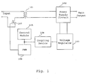
- An input voltage is applied to the input terminals.
- One of the input terminals is connected directly to a first terminal on the primary side of transformer 101.
- the other input terminal is connected to a second terminal on the primary side of transformer 101 via transistor 107.
- the input voltage applied to the primary side of transformer 101 is controlled by the switching on and off of transistor 107 in accordance with a duty cycle signal from PWM 106.
- the secondary side terminals of the transformer 101 are connected to a power supply circuit 102.
- the power supply circuit provides the main output from the SMPS as well as a power supply for voltage regulator 103.
- Voltage regulator 103 is operable to regulate the output voltage from the main output of the SMPS.
- the voltage regulator 103 receives its power supply from power supply circuit 102.
- the voltage regulator 103 switches on and operates, then a feedback signal is generated and output to coupling device 104.
- the generation of such a feedback signal is an indication that voltage regulator 103 is running and that the control module 105 should stop sending pulses to switch-on the voltage regulator.
- the feedback signal comprises the voltage regulation feedback signal which indicates a, request from the secondary side voltage regulator for an increase in duty cycle and therefore indicates that the voltage regulator has been switched on and is operating.
- the coupling device 104 is any coupling mechanism that allows transmission of the feedback signal from circuitry on the secondary side of transformer 101 to circuitry on the primary side of transformer 101 whilst maintaining the isolation between both sides of the transformer 101.
- a suitable coupling device is a wireless transmitter such as an opto-coupler.
- some SMPS designs use a coupling device to couple a signal defining the output voltage back to a controller of the duty cycle on the primary side. If such a coupling device is already present, the same coupling device may be used to transmit the feedback signal from the voltage regulator 103 to the primary side.
- the primary side output of coupling device 104 is connected to control module 105 and PWM 106.
- Control module 105 is operable to detect the presence of a feedback signal output from the coupling device 104. In dependence upon the detection of a feedback signal, the control module 105 is operable to output a control signal to the PWM 106.
- the output from the PWM 106 controls the switching of the transistor 107.
- the application of the input voltage to the primary side of transformer 101 is therefore controlled by the control module 105 via the PWM 106.
- the SMPS Before the start-up operation, the SMPS is in a state in which there has been no power transmission across transformer 101 for such time that no power is output from the main output, no power is output from the power supply circuit to the voltage regulator 103 and voltage regulator 103 is switched off.
- control module 105 controls the PWM 106 to output a single pulse.
- the pulse may be defined, for example, by the output signal from PWM 106 changing from a low voltage to a high voltage for the duration of the pulse.
- the pulse output from the PWM 106 switches on transistor 107 for the duration of the pulse so as to apply a pulse of the input voltage to the primary side of transformer 101.
- the first pulse during start-up is of generally low power which will not fully switch on the voltage regulator 103 and cause it to operate. This ensures that excess power is not provided at the main output of the power supply circuit 102.
- Filter arrangements within the power supply circuit 102 filter the received power into power for the main output and power for the voltage regulator.
- the power supply circuit 102 outputs power to voltage regulator 103 in order for voltage regulator 103 to switch and operate on before a significant amount of power has been output from the main output of the SMPS.
- the voltage regulator 103 receives power from the power supply circuit 102.
- the voltage regulator 103 If the power received from power supply circuit 102 is sufficient to switch on the voltage regulator 103 so that it operates as required, then the voltage regulator 103 generates a feedback signal that indicates that the voltage regulator 103 has switched on and is operating. Such a feedback signal would not be expected after the first pulse in normal operating conditions.
- the power received from the power supply circuit 102 is not sufficient to switch on the voltage regulator 103 (i.e. the voltage regulator 103 remains switched off or is in a state between being switched off and operating as required) then a feedback signal is not generated.
- the feedback signal When a feedback signal is generated, the feedback signal is output from voltage regulator 103 to coupling device 104 and is transmitted to the primary side.
- control module 105 If the control module 105 detects the presence of a feedback signal, it determines that the voltage regulator has switched on and is operating as required. Alternatively, if the presence of a feedback signal is not detected, the control module 105 determines that more power needs to be sent from the power supply circuit 102 to the voltage regulator 103 in order to switch on the voltage regulator 103 and to cause the voltage regulator 103 to operate as required.
- control module 105 determines that voltage regulator 103 has switched on and is operating, then the control module determines that it is not necessary to control the PWM 106 to transmit further pulses in order to ensure that the voltage regulator 103 is switched on.
- control module 105 determines that the voltage regulator 103 is not yet operating as required, then the control module controls the PWM 106 to transmit a further pulse to switch on transistor 107 for the duration of the pulse.
- a further pulse of the input power is transmitted from the primary side of transformer 101 to the secondary side and onto the power supply circuit 102.
- the filter arrangements within the power supply circuit 102 again transmit most of the received power to the voltage regulator 103 rather than the main output of the SMPS.
- Voltage regulator 103 receives the power from the second pulse and, as previously described for the first pulse, either a feedback signal is generated that indicates that the voltage regulator 103 has switched on and is operating or no such feedback signal is generated.
- the feedback signal When a feedback signal is generated, the feedback signal is output to coupling device 104 where, as described earlier, the feedback signal is transmitted to the control module 105.
- Control module 105 is operable to detect the presence of a feedback signal. In dependence upon the detection of a feedback signal, the control module 105 determines whether or not the voltage regulator has switched on and is operating, if more power needs to be sent from the power supply circuit 102 in order for voltage regulator 103 to operate as required or if an error has occurred in the start-up operation of the SMPS.
- This process is then repeated with further pulses transmitted to the secondary side, if required.
- control module 105 determines whether the voltage regulator 103 is switched on and is operating, whether a further pulse is required for the voltage regulator 103 to operate as required or if an error has occurred is shown in Figure 2 .
- step 201 the predetermined number of pulses to be sent before a determination is made that an error has occurred is set.
- a typical predetermined number of pulses is, for example, six. However, the predetermined number may be any number greater than one.
- the control module 105 controls the PWM 106 to transmit an initial pulse from the primary side to the secondary side, and the transmitted power is received by voltage regulator 103 as described above.
- step 202 the control module 105 determines whether a feedback signal has been detected, as described above, in order to determine if the voltage regulator 103 has switched on and operating (i.e. voltage regulator 103 is running).
- step 206 the control module 105 does not control PWM 106 to transmit a further pulse in order to switch on the voltage regulator 103.
- step 202 the control module 105 determines that no feedback signal is detected, then the process proceeds to step 203.
- step 203 the predetermined number of pulses to be sent before a determination is made that an error has occurred is reduced by one.
- step 204 a determination is made if the number of further pulses to be sent to switch on the voltage regulator 103 is zero.
- step 205 the control module 105 controls the PWM 106 to send a further pulse so that additional power is sent to the voltage regulator 103.
- step 202 The process then returns to step 202 to determine whether or not the voltage regulator 103 has switched and is operating.
- step 204 determines that the number of further pulses to be sent is zero, then the process proceeds to step 207 where a determination that an error has occurred is made.
- the process may return to step 201 for a new start-up attempt to be made.
- a new start-up attempt is to be made, then there is preferably a delay between the determination that an error has occurred and the start of the new start-up attempt. The delay is required to let the power that has already been sent to the main output drain away and ensures that there is no permanent voltage build-up over the main output during a fail condition.
- control module 105 controls the PWM 106 to transmit a pulse train in order to switch on voltage regulator 103, with the number of pulses transmitted being determined by the feedback signal generated by the voltage regulator 103.
- the pulse train will comprise a plurality of pulses that are sent to switch on the voltage regulator 103 until either the voltage regulator 103 switches on and operates or it is determined, after a predetermined number of pulses, that an error has occurred.
- FIG. 3 An example of a pulse train that is used in the present embodiment is shown in Figure 3 .
- the y-axis indicates whether the output from the control module 105 is high or low.
- the PWM 106 is arranged to control the transistor 107 such that a pulse of input voltage is sent from the primary side of transformer 101 to the secondary side of the transformer 101 with the same the duration as the pulses from the control module 105.
- the initial pulse of the pulse train may carry more power than any subsequent pulses.
- the power carried by a pulse may be varied either by varying the magnitude of the input voltage applied to the primary side of the transformer and/or by varying the duration for which the pulse is applied.
- the duration between the later pulses it is also preferable for the duration between the later pulses to decrease. In this way, the power supply to the voltage regulator 103 is more linear and the later pulses have an increased chance of switching-on the voltage regulator 103 so that is operates because more power is delivered by the later pulses as a whole due to the shorter time duration between them.
- the first pulse, 1 has a longer duration (resulting in higher power) than each of the subsequent pulses 2 to 6.
- control module After transmitting each of pulses 1 to 5, the control module detects for the presence of a feedback signal so as to determine if the voltage regulator has switched on or if a further pulse is required.
- the predetermined number of pulses pulse before a determination is made that an error has occurred is six.
- the control module 105 is monitoring for the presence of a feedback signal to determine if the voltage regulator has switched on and is operating or if an error has occurred.
- Described above is an apparatus in which the voltage regulator 103 is switched on with power provided by a pulse train.
- the initial pulse is set to a sufficiently low power that excess voltage does not occur at the main output of the SMPS. Accordingly, the power of the initial pulse is typically not sufficient to switch on the voltage regulator under normal operating conditions, although it may do so if there are significant variations in the operating conditions.
- pulses in the pulse train are then transmitted in accordance with a feedback signal from the voltage regulator 103 to ensure that sufficient power is provided to the voltage regulator 103 in order for it to switch on.
- the power supply circuit 102, voltage regulator 103 and control module 105 of Figure 1 are not limited to specific designs and it would be clear to the skilled person that any circuit designs that perform the above-described functions may be used.
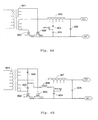
- the transformer 101 and transistor 107 shown in Figure 4 correspond to the transformer 101 and transistor 107 in Figure 1 .
- Diode 406 is connected between a terminal of transformer 101 on the secondary side and an output terminal.
- a transistor may alternatively be used.
- the power supply circuit comprises diodes 403 and 406, inductor 402, and capacitors 404 and 405.
- Inductor 402 is connected between a terminal on the secondary side of transformer 101 and an output terminal of the SMPS.
- Capacitor 405 is connected between the output terminals.
- inductor 402 and capacitor 405 provides a main output filter.
- the change in the output voltage at the output terminals is determined by the time constant of the main output filter.
- a typical time constant of such a filter is a millisecond.
- Diode 403 is connected between a tap within inductor 402 and capacitor 404.
- Capacitor 404 is connected between diode 403 and an output terminal. The junction between diode 403 and capacitor 404 provides the power supply to the voltage regulator.
- the arrangement of the inductor i.e. the inductance between the start of inductor 402 and the tap within inductor 402
- diode 403 and capacitor 403 provides a voltage regulator filter.
- the inductor acts a current limiter to protect the diode 403.
- the output voltage to the voltage regulator is determined by the time constant of the voltage regulator filter.
- the time constant of the voltage regulator filter can be set to be much lower that that of the main output filter. Accordingly, during the start-up operation, more power is output to the voltage regulator than from the main output of the SMPS.
- the voltage regulator comprises comparator 413 (which, in this example, is an operation amplifier), resistors 407, 408, 409 and 414, capacitors 411 and 412, and Zener diode 410.
- the Zener diode 410 is operable to provide a voltage reference.
- Capacitor 412 is an integrator capacitor for the voltage regulator.
- the circuit arrangement of the comparator 413, resistors 407, 408, 409, 414, capacitors 411, 412 and Zener diode 410 is an arrangement for providing output voltage regulation of an SMPS.
- An output from the power supply circuit is connected to the power supply terminal of the comparator 413 in the voltage regulator.
- Resistor 414 is directly connected to the output of the comparator. The current flowing through resistor 414 is therefore dependent upon the output of the comparator, which, in turn, is dependent upon the response of the comparator to the power received from the power supply circuit.
- the output form the voltage regulator to the coupling device 415 is therefore a feedback signal that indicates if the voltage regulator has switched on or not.
- this output signal from the voltage regulator may be a voltage error signal that is used to determine the duty cycle of the primary side switch.
- Coupling device 415 is a wireless coupling device, comprising an LED and phototransistor.
- the control module comprises controller 401, diode 417 and resistor 416.
- the PWM is provided by the component 418.
- the controller 401 and PWM 418 in Figure 4 are components with many input and output ports. Although some of the ports are shown as unconnected, the skilled person would appreciate that in use there may be connections to these ports.
- the primary side output from the coupling device 415 is directly connected to the COMP input of the PWM 418 and the PA1 input of the controller 401.
- Output PA0 from the controller is connected to the primary side output from the coupling device 415 via diode 417.
- the COMP input to PWM 218 is low and transistor 107 is not being switched by the PWM.
- Output PA0 of the controller 401 starts the start-up operation by going high for 1-3 switch pulses, for example. This causes the COMP input to the PWM 418 to go high and PWM 418 outputs a high pulse to the gate of transistor 107.
- transistor 107 In response to the high pulse from the PWM 418, transistor 107 conducts and, for the same duration of the high pulse from the PWM 418, a pulse of the input voltage is applied to the primary side of transformer 101.
- a voltage pulse is induced on the secondary side of the transformer 101 and this causes capacitor 404 to charge through diode 403 and part of the inductor 402. Capacitor 405 also charges through inductor 402.
- the voltage regulator filter Since the voltage regulator filter has a much lower time constant than the main output filter, the voltage across capacitor 404 rises much faster than that across capacitor 405.
- Capacitor 404 need not be fully charged (i.e. top filled) for sufficient power to switch on the voltage regulator to be provided.
- the current output from the voltage regulator to the LED of coupling device 415 is dependent upon the response of the voltage regulator to the power received from the power supply circuit.
- the feedback signal on the primary side which is the current generated through the phototransistor, therefore provides an indication of whether the voltage regulator has switched on as desired.
- the signal from the phototransistor is input to input PA1 of the controller 401 so the controller can determine the response of the voltage regulator.
- the controller 401 is arranged so that it does not detect the signal from the phototransistor when it is sending a control pulse to the PWM 418.
- Diode 417 is therefore provided to ensure that the state of the output PA0 does not affect the signal from the phototransistor.
- the detection of the signal from the phototransistor at input PA1 of the controller therefore allows a determination as to whether the voltage regulator has switched on and is operating, a further pulse needs to be sent or if an error has occurred.
- control of PWM 418 by controller 401 may be performed by the output PA0 toggling to a negative voltage and diode 417 having a reversed polarity.
- step 501 the process begins.
- step 502 an initial voltage pulse is transmitted from the primary side to the secondary side of the transformer so that a voltage pulse is received at a secondary side of the transformer and power in the voltage pulse is provided to the main output of the SMPS and the voltage regulator.
- step 503 a feedback signal is generated if the voltage regulator has switched on and is operating. If a feedback signal is generated, the process then proceeds to step 504 where the generated feedback signal is transmitted from circuitry on the secondary side of the transformer to circuitry on the primary side of the transformer.
- steps 503 and 504 may alternatively be performed in a single step.
- step 505 the feedback signal is detected on the primary side.
- step 506 a determination is made if the voltage regulator is operating.
- step 506 determines that a feedback signal was detected at step 505
- step 507 it is determined that the voltage regulator has switched on and is operating, and therefore the process proceeds to step 507 and ends.
- step 506 a determination is made that the voltage regulator is not operating because no feedback signal was detected at step 505, then the process proceeds to step 508.
- step 508 a determination is made if a predetermined number of voltage pulses have been sent.
- step 502 If a predetermined number of voltage pulses have not been sent, then the process returns to step 502 and a further voltage pulse is sent from the primary side to the secondary side of the transformer.
- step 508 a determination is made that a predetermined number of voltage pulses have been sent, then the process proceeds to step 509 where a determination is made that an error in the start-up operation has occurred.
- step 510 The process then proceeds to step 510 and waits for a predetermined delay to ensure that any voltage at the main output of the SMPS has drained away.
- the predetermined number of voltage pulses to be sent before an error is determined is reset and the process returns to step 502 to start a new start-up operation.
- FIGS 6A and 6B are alternative designs and arrangements of power supply circuit and transformer from that shown in Figure 4 .
- Both of the circuits in Figure 6A and 6B differ from that in Figure 4 in that a tap on the secondary side of the transformer is fed to the power supply circuit rather than both of the end terminals.
- connection to any of the taps of the transformer can be varied as required.
- transistors are provided at each terminal of the secondary side of the transformer.
- This shared inductor arrangement is the same as that already used in the power supply circuit of Figure 4 .
- the inductance of the inductor of the main output filter is set by the entire length of inductor 402.
- the inductance of the inductor of the voltage regulator filter is set by just part of the length of the inductor 402.
- the setting of the time constants of each filter is more restrictive and so a high transformer voltage may be required before the required voltage is output to the voltage regulator circuit.
- FIG. 6B differs from that in Figure 6A in that the filters do not share part of the same inductor.
- Inductor 607 and capacitor 405 provide the main output filter of the SMPS.
- Inductor 606 and capacitor 404 provide the voltage regulator filter.
- the separate inductors allow more flexibility in the setting of the time constants of each filter and so it is easier to output a desired voltage to the voltage regulator.
- the power supply circuit in Figure 6B requires more components.
- the voltage regulator 103 only generates a feedback signal when the voltage regulator 103 is switched on and operating.
- a feedback signal is generated that represents the current state of the voltage regulator 103.
- the feedback signal is generated and output to coupling device 104 and transmitted to the primary side either continuously or after each voltage pulse.
- the control module 105 is arranged to monitor the feedback signal on the primary side. If the feedback signal has a voltage or current magnitude above a predetermined level, for example, then this provides an indication that the voltage regulator has switched on and is operating as required. Alternatively, if the feedback signal has a voltage or current magnitude below a predetermined level, for example, then this provides an indication that the voltage regulator needs more power to operate as required.
- the level of the feedback signal (i.e. current or voltage magnitude) represents the response of the voltage regulator 103 to received power. Accordingly, in this modification, the control module 105 monitors a level of the feedback signal and determines if the voltage regulator 103 has switched-on and is operating in dependence upon the level of feedback signal rather than making such a determination on the detection of the presence of a feedback signal.
- the power in the initial pulse for switching on the voltage regulator prefferably be set at a level which is high enough to switch on the voltage regulator under normal operating conditions. Subsequent pulses to switch on the voltage regulator would then only be required under significantly different operating conditions.
- the pattern of the pulse train is defined by the width of each pulse, the duration between each pulse and the predetermined number of pulses to be transmitted before a determination is made that an error has occurred. It is possible for a number of pulse train patterns to be defined and for a pattern to be selected for a start-up operation in dependence upon at least one operating condition (such as input voltage or temperature) of the SMPS. Accordingly, a pulse train with the most appropriate pattern for the environment is applied.
- each pulse is defined by a continuous high signal.
- one or more of the pulses may be defined by a burst (i.e. a series of short high signals).
- control module 105 is shown as a separate unit from the PWM 106.
- control module may be incorporated into the PWM 106 so that the control module and PWM are housed in a single circuit.
- control module 105 detected the feedback signal after transmitting each pulse.
- control module is not restricted to detecting the control signal after each pulse and may, for example, detect the feedback signal after every other pulse.
- the type of SMPS was a DC/DC converter.
- the embodiment could alternatively have been described with an AC/DC converter (rectifier) type of SMPS.
Claims (13)
- Alimentation à découpage comprenant :un transformateur (101) ayant un côté primaire et un côté secondaire ;une sortie principale de l'alimentation à découpage agencée sur le côté secondaire ;un régulateur de tension (103) agencé sur le côté secondaire et ayant pour fonction de réguler la tension de sortie à la sortie principale de l'alimentation à découpage ;un circuit d'alimentation électrique (102) agencé pour fournir une alimentation électrique sur le côté secondaire, le circuit d'alimentation électrique (102) ayant pour fonction de recevoir une puissance à partir du côté primaire via le transformateur (101) et de délivrer en sortie une puissance à la sortie principale et également au régulateur de tension (103) ;un module de commande (105) sur le côté primaire ayant pour fonction de commander un modulateur de largeur d'impulsion (106) pour envoyer un train d'impulsions de tension à partir du côté primaire au côté secondaire via le transformateur (101) afin de mettre en marche le régulateur de tension (103) ; etun dispositif de couplage (104) ayant pour fonction de transmettre un signal de rétroaction à partir du côté secondaire au côté primaire, dans lequel le signal de rétroaction est généré en fonction de la réponse du régulateur de tension (103) à la puissance reçue à partir du circuit d'alimentation électrique (102) ;dans laquelle le module de commande (105) a pour fonction de détecter le signal de rétroaction pour déterminer si le régulateur de tension (103) est mis en marche et fonctionne, et de déterminer si une impulsion supplémentaire dans le train d'impulsions doit être transmise à partir du côté primaire au côté secondaire en fonction de la détection du signal de rétroaction ; etle module de commande (105) est agencé pour commander le modulateur de largeur d'impulsion (106) pour transmettre le train d'impulsions de sorte que la première impulsion parmi les impulsions possède une puissance supérieure à l'une des impulsions suivantes dans le train d'impulsions.
- Alimentation à découpage selon la revendication 1, dans laquelle le module de commande (105) est agencé pour commander le modulateur de largeur d'impulsion (106) pour arrêter la transmission d'impulsions dans le train d'impulsions afin de mettre en marche le régulateur de tension (103) lorsque soit un signal de rétroaction a été détecté indiquant que le régulateur de tension (103) est mis en marche et fonctionne, soit un nombre prédéterminé d'impulsions a été transmis.
- Alimentation à découpage selon la revendication 1 ou 2, dans laquelle le module de commande (105) est agencé pour commander le modulateur de largeur d'impulsion (106) pour transmettre le train d'impulsions de sorte que la première impulsion parmi les impulsions possède une durée plus longue que l'une des impulsions suivantes dans le train d'impulsions.
- Alimentation à découpage selon l'une des revendications précédentes, dans laquelle le module de commande (105) a pour fonction de commander le modulateur de largeur d'impulsion (106) pour transmettre un train d'impulsions comprenant au moins trois impulsions de sorte que la durée entre les deux premières impulsions du train soit supérieure à la durée entre les deux dernières impulsions du train.
- Alimentation à découpage selon l'une des revendications précédentes, dans laquelle le module de commande (105) est agencé pour déterminer qu'une erreur s'est produite si un nombre prédéterminé d'impulsions a été transmis et un signal de rétroaction n'a pas été reçu indiquant que le régulateur de tension (103) est mis en marche et fonctionne.
- Alimentation à découpage selon l'une des revendications précédentes, dans laquelle le signal de rétroaction et la sortie du module de commande (401) pour commander le modulateur de largeur d'impulsion (418) sont introduits à la même entrée du modulateur de largeur d'impulsion (418), et une diode (417) est agencée entre ladite entrée du modulateur de largeur d'impulsion et la sortie du module de commande (401) de sorte qu'un courant ne circule pas entre la sortie de module de commande et le modulateur de largeur d'impulsion (418) lorsque le module de commande (401) n'envoie pas un signal de commande au modulateur de largeur d'impulsion (418).
- Alimentation à découpage selon l'une des revendications précédentes, dans laquelle le module de commande (105, 418) fait partie du modulateur de largeur d'impulsion.
- Alimentation à découpage selon l'une des revendications précédentes, l'alimentation à découpage comprenant en outre un moyen pour stocker une pluralité de différents motifs pour un train d'impulsions, un motif pour un train d'impulsions étant défini par la largeur de chaque impulsion, la durée entre chaque impulsion et un nombre prédéterminé d'impulsions à transmettre avant une détermination selon laquelle une erreur s'est produite ; et
dans laquelle le module de commande a pour fonction de sélectionner un motif d'un train d'impulsions afin de mettre en marche le régulateur de tension en fonction d'au moins une condition de fonctionnement de l'alimentation à découpage. - Procédé de fonctionnement d'une alimentation à découpage ayant un transformateur (101) avec un côté primaire et un côté secondaire, une sortie principale de l'alimentation à découpage étant agencée sur le côté secondaire, et un régulateur de tension (103) agencé sur le côté secondaire pour recevoir une puissance à partir du côté primaire et pour réguler la tension de sortie à la sortie principale de l'alimentation à découpage, le procédé étant exécuté pour mettre en marche le régulateur de tension et comprenant le fait :de transmettre (502) une impulsion de tension à partir du côté primaire au côté secondaire du transformateur de sorte que l'impulsion de tension soit reçue au niveau du côté secondaire du transformateur et la puissance dans l'impulsion de tension soit fournie à la sortie principale de l'alimentation à découpage et au régulateur de tension ;de générer (504), lorsque le régulateur de tension est mis en marche et fonctionne par l'impulsion de tension, un signal de rétroaction indiquant que le régulateur de tension est mis en marche et fonctionne,de transmettre (505) le signal de rétroaction à partir du côté secondaire au côté primaire ;de déterminer si (506) un signal de rétroaction a été détecté sur le côté primaire indiquant que le régulateur de tension est mis en marche et fonctionne ;de transmettre, lorsqu'aucun signal de rétroaction n'est détecté sur le côté primaire indiquant que le régulateur de tension est mis en marche et fonctionne, une impulsion supplémentaire à partir du côté primaire au côté secondaire ; etde cesser de transmettre, lorsqu'un signal de rétroaction est détecté sur le côté primaire indiquant que le régulateur de tension est mis en marche et fonctionne, des impulsions de tension à partir du côté primaire pour mettre en marche le régulateur de tension ;dans lequel la première impulsion transmise à partir du côté primaire au côté secondaire du transformateur a une puissance supérieure à une impulsion suivante quelconque.
- Procédé selon la revendication 10, dans lequel des impulsions sont transmises à partir du côté primaire au côté secondaire afin de démarrer le régulateur de tension jusqu'à ce qu'une détermination soit faite selon laquelle un signal de rétroaction a été détecté sur le côté primaire indiquant que le régulateur de tension est mis en marche et fonctionne ou selon laquelle un nombre prédéterminé d'impulsions a été transmis.
- Procédé selon la revendication 9 ou 10, dans lequel la première impulsion est transmise avec une durée plus longue qu'une impulsion suivante quelconque.
- Procédé selon l'une des revendications 9 à 11, dans lequel au moins trois impulsions sont transmises à partir du côté primaire au côté secondaire du transformateur et la durée entre les deux premières impulsions est supérieure à la durée entre les deux dernières impulsions.
- Procédé selon l'une des revendications 9 à 12, dans lequel :une pluralité de différents motifs pour un train d'impulsions sont stockés, un motif pour un train d'impulsions étant défini par la largeur de chaque impulsion, la durée entre chaque impulsion et le nombre prédéterminé d'impulsions à transmettre avant une détermination selon laquelle une erreur s'est produite ; etun motif d'un train d'impulsions à transmettre afin de mettre en marche le régulateur de tension est choisi en fonction d'au moins une condition de fonctionnement de l'alimentation à découpage.
Applications Claiming Priority (1)
| Application Number | Priority Date | Filing Date | Title |
|---|---|---|---|
| PCT/EP2010/054192 WO2011120558A1 (fr) | 2010-03-30 | 2010-03-30 | Alimentation à découpage pourvue d'un régulateur de tension |
Publications (2)
| Publication Number | Publication Date |
|---|---|
| EP2553798A1 EP2553798A1 (fr) | 2013-02-06 |
| EP2553798B1 true EP2553798B1 (fr) | 2014-12-03 |
Family
ID=43468605
Family Applications (1)
| Application Number | Title | Priority Date | Filing Date |
|---|---|---|---|
| EP10713162.5A Active EP2553798B1 (fr) | 2010-03-30 | 2010-03-30 | Alimentation à découpage pourvue d'un régulateur de tension |
Country Status (4)
| Country | Link |
|---|---|
| US (1) | US8964416B2 (fr) |
| EP (1) | EP2553798B1 (fr) |
| CN (1) | CN102812627B (fr) |
| WO (1) | WO2011120558A1 (fr) |
Families Citing this family (11)
| Publication number | Priority date | Publication date | Assignee | Title |
|---|---|---|---|---|
| US10036768B2 (en) * | 2011-08-29 | 2018-07-31 | Landis+Gyr Llc | Method and arrangement for controlling DC power output in utility meter |
| US9024603B2 (en) | 2012-02-01 | 2015-05-05 | Conexant Systems, Inc. | Low power current comparator for switched mode regulator |
| CN106415547B (zh) * | 2014-03-31 | 2020-03-20 | 瑞典爱立信有限公司 | 开关模式电源输出滤波器配置 |
| US9819274B2 (en) * | 2014-11-20 | 2017-11-14 | Microchip Technology Incorporated | Start-up controller for a power converter |
| US9825546B2 (en) * | 2016-03-30 | 2017-11-21 | Infineon Technologies Austria Ag | Circuits and methods for auxiliary secondary supply generation with self-starting primary side driver in isolated power converters |
| US10355602B2 (en) * | 2017-01-18 | 2019-07-16 | Analog Devices Global | Fault suppression or recovery for isolated conversion |
| GB2560045B (en) * | 2017-02-28 | 2019-10-30 | Cirrus Logic Int Semiconductor Ltd | Amplifiers |
| US10803909B2 (en) * | 2018-08-24 | 2020-10-13 | Micron Technology, Inc. | Power management component for memory sub system power cycling |
| FR3087064B1 (fr) * | 2018-10-09 | 2020-11-20 | Stmicroelectronics Razvoj Polprevodnikov D O O | Source d'alimentation a decoupage d'un lecteur du type communication en champ proche |
| US11536754B2 (en) | 2019-08-15 | 2022-12-27 | Landis+Gyr Innovations, Inc. | Electricity meter with fault tolerant power supply |
| CN112977173B (zh) * | 2021-04-30 | 2022-05-03 | 重庆长安新能源汽车科技有限公司 | 一种电动汽车及其动力电池脉冲加热系统和加热方法 |
Family Cites Families (5)
| Publication number | Priority date | Publication date | Assignee | Title |
|---|---|---|---|---|
| US3959714A (en) * | 1973-09-24 | 1976-05-25 | Sperry Rand Corporation | Transient turn-on protection circuit for power supplies |
| FR2577360B1 (fr) * | 1985-02-08 | 1987-03-06 | Thomson Csf | Circuit de commande d'alimentation a decoupage a demarrage automatique |
| KR101365753B1 (ko) | 2007-04-23 | 2014-02-21 | 페어차일드코리아반도체 주식회사 | 컨버터 및 그 구동방법 |
| US8125800B2 (en) | 2007-10-17 | 2012-02-28 | Texas Instruments Incorporated | Secondary-side amplifier with soft start |
| EP2289159B1 (fr) * | 2008-06-17 | 2019-01-30 | Telefonaktiebolaget LM Ericsson (publ) | Convertisseur de puissance |
-
2010
- 2010-03-30 EP EP10713162.5A patent/EP2553798B1/fr active Active
- 2010-03-30 WO PCT/EP2010/054192 patent/WO2011120558A1/fr active Application Filing
- 2010-03-30 CN CN201080065868.XA patent/CN102812627B/zh active Active
- 2010-03-30 US US13/635,197 patent/US8964416B2/en active Active
Also Published As
| Publication number | Publication date |
|---|---|
| WO2011120558A1 (fr) | 2011-10-06 |
| CN102812627B (zh) | 2016-02-03 |
| CN102812627A (zh) | 2012-12-05 |
| EP2553798A1 (fr) | 2013-02-06 |
| US8964416B2 (en) | 2015-02-24 |
| US20130003422A1 (en) | 2013-01-03 |
Similar Documents
| Publication | Publication Date | Title |
|---|---|---|
| EP2553798B1 (fr) | Alimentation à découpage pourvue d'un régulateur de tension | |
| US11888402B2 (en) | Controller for multi-output single magnetic component converter | |
| US8854842B2 (en) | Digital communication link between secondary side and primary side of switching power converter | |
| CN106063104B (zh) | 开关受控谐振dc-dc电力转换器 | |
| US8885364B2 (en) | Flyback converter with primary side and secondary side feedback control and method for the same | |
| JP5253304B2 (ja) | エネルギ伝達エレメントの入力にわたる電圧から導かれた電流に応答するための回路および方法 | |
| CN1941586B (zh) | 节能开关电源设备及其节能方法 | |
| US8374004B2 (en) | Isolated AC-DC converter with master controller on secondary side and slave controller on primary side | |
| CN107534389B (zh) | 切换输出电压的设定的开关电源装置和开关电源装置用集成电路 | |
| CN101908823A (zh) | 限制开关电源中输出功率的方法和装置 | |
| WO2012061059A1 (fr) | Système de commande de démarrage souple et procédé pour convertisseur continu-continu isolé à unité de commande secondaire | |
| JP2008541688A (ja) | スイッチモード電源のための帰還情報伝達技術 | |
| US10784707B2 (en) | Inductive power transfer system | |
| JP5319137B2 (ja) | Dcdc変換器、及びこれに用いた電圧検出装置 | |
| EP2697900B1 (fr) | Allimentation a découpage avec une alimentation au démarrage simplifiee | |
| WO2007063788A1 (fr) | Dispositif d’alimentation électrique à découpage et procédé de démarrage de celui-ci | |
| WO2010125751A1 (fr) | Dispositif de commutation d'alimentation électrique | |
| JP2020188538A (ja) | 電源装置及び画像形成装置 | |
| JP6609445B2 (ja) | ワイヤレス送電装置、その制御回路および制御方法、充電器 | |
| CN112994465B (zh) | 电源供应装置及其控制方法 | |
| KR101454486B1 (ko) | 다중 출력 전원 장치 | |
| EP3416271B1 (fr) | Appareils et procédés d'alimentation électrique à commande de sortie pour des terminaux multiples | |
| KR20130083601A (ko) | 과전압 보호 기능을 갖는 스위칭 모드 전원 장치 | |
| KR20170103459A (ko) | 플라이백 컨버터 |
Legal Events
| Date | Code | Title | Description |
|---|---|---|---|
| PUAI | Public reference made under article 153(3) epc to a published international application that has entered the european phase |
Free format text: ORIGINAL CODE: 0009012 |
|
| 17P | Request for examination filed |
Effective date: 20120720 |
|
| AK | Designated contracting states |
Kind code of ref document: A1 Designated state(s): AT BE BG CH CY CZ DE DK EE ES FI FR GB GR HR HU IE IS IT LI LT LU LV MC MK MT NL NO PL PT RO SE SI SK SM TR |
|
| DAX | Request for extension of the european patent (deleted) | ||
| REG | Reference to a national code |
Ref country code: DE Ref legal event code: R079 Ref document number: 602010020695 Country of ref document: DE Free format text: PREVIOUS MAIN CLASS: H02M0003335000 Ipc: H02M0001420000 |
|
| GRAP | Despatch of communication of intention to grant a patent |
Free format text: ORIGINAL CODE: EPIDOSNIGR1 |
|
| INTG | Intention to grant announced |
Effective date: 20140708 |
|
| RIC1 | Information provided on ipc code assigned before grant |
Ipc: H02M 1/42 20070101AFI20140630BHEP |
|
| GRAS | Grant fee paid |
Free format text: ORIGINAL CODE: EPIDOSNIGR3 |
|
| GRAA | (expected) grant |
Free format text: ORIGINAL CODE: 0009210 |
|
| RAP1 | Party data changed (applicant data changed or rights of an application transferred) |
Owner name: TELEFONAKTIEBOLAGET L M ERICSSON (PUBL) |
|
| AK | Designated contracting states |
Kind code of ref document: B1 Designated state(s): AT BE BG CH CY CZ DE DK EE ES FI FR GB GR HR HU IE IS IT LI LT LU LV MC MK MT NL NO PL PT RO SE SI SK SM TR |
|
| REG | Reference to a national code |
Ref country code: GB Ref legal event code: FG4D |
|
| REG | Reference to a national code |
Ref country code: AT Ref legal event code: REF Ref document number: 699867 Country of ref document: AT Kind code of ref document: T Effective date: 20141215 Ref country code: CH Ref legal event code: EP |
|
| REG | Reference to a national code |
Ref country code: IE Ref legal event code: FG4D |
|
| REG | Reference to a national code |
Ref country code: DE Ref legal event code: R096 Ref document number: 602010020695 Country of ref document: DE Effective date: 20150115 |
|
| REG | Reference to a national code |
Ref country code: NL Ref legal event code: VDEP Effective date: 20141203 |
|
| REG | Reference to a national code |
Ref country code: AT Ref legal event code: MK05 Ref document number: 699867 Country of ref document: AT Kind code of ref document: T Effective date: 20141203 |
|
| PG25 | Lapsed in a contracting state [announced via postgrant information from national office to epo] |
Ref country code: ES Free format text: LAPSE BECAUSE OF FAILURE TO SUBMIT A TRANSLATION OF THE DESCRIPTION OR TO PAY THE FEE WITHIN THE PRESCRIBED TIME-LIMIT Effective date: 20141203 Ref country code: NL Free format text: LAPSE BECAUSE OF FAILURE TO SUBMIT A TRANSLATION OF THE DESCRIPTION OR TO PAY THE FEE WITHIN THE PRESCRIBED TIME-LIMIT Effective date: 20141203 Ref country code: LT Free format text: LAPSE BECAUSE OF FAILURE TO SUBMIT A TRANSLATION OF THE DESCRIPTION OR TO PAY THE FEE WITHIN THE PRESCRIBED TIME-LIMIT Effective date: 20141203 Ref country code: NO Free format text: LAPSE BECAUSE OF FAILURE TO SUBMIT A TRANSLATION OF THE DESCRIPTION OR TO PAY THE FEE WITHIN THE PRESCRIBED TIME-LIMIT Effective date: 20150303 Ref country code: FI Free format text: LAPSE BECAUSE OF FAILURE TO SUBMIT A TRANSLATION OF THE DESCRIPTION OR TO PAY THE FEE WITHIN THE PRESCRIBED TIME-LIMIT Effective date: 20141203 |
|
| REG | Reference to a national code |
Ref country code: LT Ref legal event code: MG4D |
|
| PG25 | Lapsed in a contracting state [announced via postgrant information from national office to epo] |
Ref country code: SE Free format text: LAPSE BECAUSE OF FAILURE TO SUBMIT A TRANSLATION OF THE DESCRIPTION OR TO PAY THE FEE WITHIN THE PRESCRIBED TIME-LIMIT Effective date: 20141203 Ref country code: GR Free format text: LAPSE BECAUSE OF FAILURE TO SUBMIT A TRANSLATION OF THE DESCRIPTION OR TO PAY THE FEE WITHIN THE PRESCRIBED TIME-LIMIT Effective date: 20150304 Ref country code: HR Free format text: LAPSE BECAUSE OF FAILURE TO SUBMIT A TRANSLATION OF THE DESCRIPTION OR TO PAY THE FEE WITHIN THE PRESCRIBED TIME-LIMIT Effective date: 20141203 Ref country code: AT Free format text: LAPSE BECAUSE OF FAILURE TO SUBMIT A TRANSLATION OF THE DESCRIPTION OR TO PAY THE FEE WITHIN THE PRESCRIBED TIME-LIMIT Effective date: 20141203 Ref country code: LV Free format text: LAPSE BECAUSE OF FAILURE TO SUBMIT A TRANSLATION OF THE DESCRIPTION OR TO PAY THE FEE WITHIN THE PRESCRIBED TIME-LIMIT Effective date: 20141203 Ref country code: CY Free format text: LAPSE BECAUSE OF FAILURE TO SUBMIT A TRANSLATION OF THE DESCRIPTION OR TO PAY THE FEE WITHIN THE PRESCRIBED TIME-LIMIT Effective date: 20141203 |
|
| PG25 | Lapsed in a contracting state [announced via postgrant information from national office to epo] |
Ref country code: EE Free format text: LAPSE BECAUSE OF FAILURE TO SUBMIT A TRANSLATION OF THE DESCRIPTION OR TO PAY THE FEE WITHIN THE PRESCRIBED TIME-LIMIT Effective date: 20141203 Ref country code: SK Free format text: LAPSE BECAUSE OF FAILURE TO SUBMIT A TRANSLATION OF THE DESCRIPTION OR TO PAY THE FEE WITHIN THE PRESCRIBED TIME-LIMIT Effective date: 20141203 Ref country code: CZ Free format text: LAPSE BECAUSE OF FAILURE TO SUBMIT A TRANSLATION OF THE DESCRIPTION OR TO PAY THE FEE WITHIN THE PRESCRIBED TIME-LIMIT Effective date: 20141203 Ref country code: PT Free format text: LAPSE BECAUSE OF FAILURE TO SUBMIT A TRANSLATION OF THE DESCRIPTION OR TO PAY THE FEE WITHIN THE PRESCRIBED TIME-LIMIT Effective date: 20150403 Ref country code: RO Free format text: LAPSE BECAUSE OF FAILURE TO SUBMIT A TRANSLATION OF THE DESCRIPTION OR TO PAY THE FEE WITHIN THE PRESCRIBED TIME-LIMIT Effective date: 20141203 |
|
| PG25 | Lapsed in a contracting state [announced via postgrant information from national office to epo] |
Ref country code: PL Free format text: LAPSE BECAUSE OF FAILURE TO SUBMIT A TRANSLATION OF THE DESCRIPTION OR TO PAY THE FEE WITHIN THE PRESCRIBED TIME-LIMIT Effective date: 20141203 Ref country code: IS Free format text: LAPSE BECAUSE OF FAILURE TO SUBMIT A TRANSLATION OF THE DESCRIPTION OR TO PAY THE FEE WITHIN THE PRESCRIBED TIME-LIMIT Effective date: 20150403 |
|
| REG | Reference to a national code |
Ref country code: DE Ref legal event code: R097 Ref document number: 602010020695 Country of ref document: DE |
|
| PLBE | No opposition filed within time limit |
Free format text: ORIGINAL CODE: 0009261 |
|
| STAA | Information on the status of an ep patent application or granted ep patent |
Free format text: STATUS: NO OPPOSITION FILED WITHIN TIME LIMIT |
|
| PG25 | Lapsed in a contracting state [announced via postgrant information from national office to epo] |
Ref country code: DK Free format text: LAPSE BECAUSE OF FAILURE TO SUBMIT A TRANSLATION OF THE DESCRIPTION OR TO PAY THE FEE WITHIN THE PRESCRIBED TIME-LIMIT Effective date: 20141203 Ref country code: MC Free format text: LAPSE BECAUSE OF FAILURE TO SUBMIT A TRANSLATION OF THE DESCRIPTION OR TO PAY THE FEE WITHIN THE PRESCRIBED TIME-LIMIT Effective date: 20141203 Ref country code: LU Free format text: LAPSE BECAUSE OF FAILURE TO SUBMIT A TRANSLATION OF THE DESCRIPTION OR TO PAY THE FEE WITHIN THE PRESCRIBED TIME-LIMIT Effective date: 20150330 |
|
| REG | Reference to a national code |
Ref country code: CH Ref legal event code: PL |
|
| 26N | No opposition filed |
Effective date: 20150904 |
|
| REG | Reference to a national code |
Ref country code: IE Ref legal event code: MM4A |
|
| PG25 | Lapsed in a contracting state [announced via postgrant information from national office to epo] |
Ref country code: CH Free format text: LAPSE BECAUSE OF NON-PAYMENT OF DUE FEES Effective date: 20150331 Ref country code: IE Free format text: LAPSE BECAUSE OF NON-PAYMENT OF DUE FEES Effective date: 20150330 Ref country code: LI Free format text: LAPSE BECAUSE OF NON-PAYMENT OF DUE FEES Effective date: 20150331 |
|
| PG25 | Lapsed in a contracting state [announced via postgrant information from national office to epo] |
Ref country code: SI Free format text: LAPSE BECAUSE OF FAILURE TO SUBMIT A TRANSLATION OF THE DESCRIPTION OR TO PAY THE FEE WITHIN THE PRESCRIBED TIME-LIMIT Effective date: 20141203 |
|
| REG | Reference to a national code |
Ref country code: FR Ref legal event code: PLFP Year of fee payment: 7 |
|
| PG25 | Lapsed in a contracting state [announced via postgrant information from national office to epo] |
Ref country code: BE Free format text: LAPSE BECAUSE OF FAILURE TO SUBMIT A TRANSLATION OF THE DESCRIPTION OR TO PAY THE FEE WITHIN THE PRESCRIBED TIME-LIMIT Effective date: 20141203 |
|
| PG25 | Lapsed in a contracting state [announced via postgrant information from national office to epo] |
Ref country code: MT Free format text: LAPSE BECAUSE OF FAILURE TO SUBMIT A TRANSLATION OF THE DESCRIPTION OR TO PAY THE FEE WITHIN THE PRESCRIBED TIME-LIMIT Effective date: 20141203 |
|
| REG | Reference to a national code |
Ref country code: FR Ref legal event code: PLFP Year of fee payment: 8 |
|
| PG25 | Lapsed in a contracting state [announced via postgrant information from national office to epo] |
Ref country code: SM Free format text: LAPSE BECAUSE OF FAILURE TO SUBMIT A TRANSLATION OF THE DESCRIPTION OR TO PAY THE FEE WITHIN THE PRESCRIBED TIME-LIMIT Effective date: 20141203 Ref country code: BG Free format text: LAPSE BECAUSE OF FAILURE TO SUBMIT A TRANSLATION OF THE DESCRIPTION OR TO PAY THE FEE WITHIN THE PRESCRIBED TIME-LIMIT Effective date: 20141203 Ref country code: HU Free format text: LAPSE BECAUSE OF FAILURE TO SUBMIT A TRANSLATION OF THE DESCRIPTION OR TO PAY THE FEE WITHIN THE PRESCRIBED TIME-LIMIT; INVALID AB INITIO Effective date: 20100330 |
|
| PG25 | Lapsed in a contracting state [announced via postgrant information from national office to epo] |
Ref country code: TR Free format text: LAPSE BECAUSE OF FAILURE TO SUBMIT A TRANSLATION OF THE DESCRIPTION OR TO PAY THE FEE WITHIN THE PRESCRIBED TIME-LIMIT Effective date: 20141203 |
|
| REG | Reference to a national code |
Ref country code: FR Ref legal event code: PLFP Year of fee payment: 9 |
|
| PG25 | Lapsed in a contracting state [announced via postgrant information from national office to epo] |
Ref country code: MK Free format text: LAPSE BECAUSE OF FAILURE TO SUBMIT A TRANSLATION OF THE DESCRIPTION OR TO PAY THE FEE WITHIN THE PRESCRIBED TIME-LIMIT Effective date: 20141203 |
|
| PGFP | Annual fee paid to national office [announced via postgrant information from national office to epo] |
Ref country code: IT Payment date: 20190124 Year of fee payment: 19 |
|
| PG25 | Lapsed in a contracting state [announced via postgrant information from national office to epo] |
Ref country code: IT Free format text: LAPSE BECAUSE OF NON-PAYMENT OF DUE FEES Effective date: 20200330 |
|
| PGFP | Annual fee paid to national office [announced via postgrant information from national office to epo] |
Ref country code: FR Payment date: 20230327 Year of fee payment: 14 |
|
| PGFP | Annual fee paid to national office [announced via postgrant information from national office to epo] |
Ref country code: GB Payment date: 20230327 Year of fee payment: 14 Ref country code: DE Payment date: 20230329 Year of fee payment: 14 |