EP2553314B1 - Led-lampe zur homogenen ausleuchtung von hohlkörpern - Google Patents
Led-lampe zur homogenen ausleuchtung von hohlkörpern Download PDFInfo
- Publication number
- EP2553314B1 EP2553314B1 EP11713180.5A EP11713180A EP2553314B1 EP 2553314 B1 EP2553314 B1 EP 2553314B1 EP 11713180 A EP11713180 A EP 11713180A EP 2553314 B1 EP2553314 B1 EP 2553314B1
- Authority
- EP
- European Patent Office
- Prior art keywords
- chip
- leds
- board led
- lighting apparatus
- led module
- Prior art date
- Legal status (The legal status is an assumption and is not a legal conclusion. Google has not performed a legal analysis and makes no representation as to the accuracy of the status listed.)
- Active
Links
Images


Classifications
-
- F—MECHANICAL ENGINEERING; LIGHTING; HEATING; WEAPONS; BLASTING
- F21—LIGHTING
- F21K—NON-ELECTRIC LIGHT SOURCES USING LUMINESCENCE; LIGHT SOURCES USING ELECTROCHEMILUMINESCENCE; LIGHT SOURCES USING CHARGES OF COMBUSTIBLE MATERIAL; LIGHT SOURCES USING SEMICONDUCTOR DEVICES AS LIGHT-GENERATING ELEMENTS; LIGHT SOURCES NOT OTHERWISE PROVIDED FOR
- F21K9/00—Light sources using semiconductor devices as light-generating elements, e.g. using light-emitting diodes [LED] or lasers
- F21K9/20—Light sources comprising attachment means
-
- F—MECHANICAL ENGINEERING; LIGHTING; HEATING; WEAPONS; BLASTING
- F21—LIGHTING
- F21V—FUNCTIONAL FEATURES OR DETAILS OF LIGHTING DEVICES OR SYSTEMS THEREOF; STRUCTURAL COMBINATIONS OF LIGHTING DEVICES WITH OTHER ARTICLES, NOT OTHERWISE PROVIDED FOR
- F21V19/00—Fastening of light sources or lamp holders
- F21V19/001—Fastening of light sources or lamp holders the light sources being semiconductors devices, e.g. LEDs
-
- F—MECHANICAL ENGINEERING; LIGHTING; HEATING; WEAPONS; BLASTING
- F21—LIGHTING
- F21V—FUNCTIONAL FEATURES OR DETAILS OF LIGHTING DEVICES OR SYSTEMS THEREOF; STRUCTURAL COMBINATIONS OF LIGHTING DEVICES WITH OTHER ARTICLES, NOT OTHERWISE PROVIDED FOR
- F21V23/00—Arrangement of electric circuit elements in or on lighting devices
- F21V23/003—Arrangement of electric circuit elements in or on lighting devices the elements being electronics drivers or controllers for operating the light source, e.g. for a LED array
-
- F—MECHANICAL ENGINEERING; LIGHTING; HEATING; WEAPONS; BLASTING
- F21—LIGHTING
- F21V—FUNCTIONAL FEATURES OR DETAILS OF LIGHTING DEVICES OR SYSTEMS THEREOF; STRUCTURAL COMBINATIONS OF LIGHTING DEVICES WITH OTHER ARTICLES, NOT OTHERWISE PROVIDED FOR
- F21V23/00—Arrangement of electric circuit elements in or on lighting devices
- F21V23/04—Arrangement of electric circuit elements in or on lighting devices the elements being switches
-
- F—MECHANICAL ENGINEERING; LIGHTING; HEATING; WEAPONS; BLASTING
- F21—LIGHTING
- F21Y—INDEXING SCHEME ASSOCIATED WITH SUBCLASSES F21K, F21L, F21S and F21V, RELATING TO THE FORM OR THE KIND OF THE LIGHT SOURCES OR OF THE COLOUR OF THE LIGHT EMITTED
- F21Y2107/00—Light sources with three-dimensionally disposed light-generating elements
- F21Y2107/30—Light sources with three-dimensionally disposed light-generating elements on the outer surface of cylindrical surfaces, e.g. rod-shaped supports having a circular or a polygonal cross section
-
- F—MECHANICAL ENGINEERING; LIGHTING; HEATING; WEAPONS; BLASTING
- F21—LIGHTING
- F21Y—INDEXING SCHEME ASSOCIATED WITH SUBCLASSES F21K, F21L, F21S and F21V, RELATING TO THE FORM OR THE KIND OF THE LIGHT SOURCES OR OF THE COLOUR OF THE LIGHT EMITTED
- F21Y2115/00—Light-generating elements of semiconductor light sources
- F21Y2115/10—Light-emitting diodes [LED]
Definitions
- the invention relates to a lighting device for uniform illumination of curved, non-planar or polyhedral surfaces, comprising a plurality of planar chip-on-board LED modules, which are arranged adjacent to each other at least in pairs, wherein each chip-on-board LED module a Comprising a plurality of light emitting LEDs.
- the invention further relates to a lighting unit and a use.
- sewer rehabilitation where it is known to provide the inside of pipes or hoses with a photohardenable coating or substance in the form of a hose.
- a so-called "tube liner” a resin-impregnated glass fiber fabric with protective plastic films on the outer surfaces of a sewer rehabilitation a lamp is forced through the tube or pipe through to progressively dry and cure the coating material in sections by means of intense lighting.
- Corresponding lamp systems are ideally bendable for bends up to 90 °. Typical diameters of coated tubes and hoses are in the range of a few centimeters to several meters.
- Typical homogeneity tolerances for illumination are in the range of less than ⁇ 15% with respect to a defined mean.
- the irradiances on an illuminated inner wall are for this application a few ⁇ W / cm 2 up to 100 W / cm 2 .
- corresponding known lamp systems are provided with a diameter which is only a few millimeters below the pipe inside diameter for which they are designed.
- the lamp can also be up to a few meters from the surface to be irradiated.
- gas discharge lamps which provide an intense light output.
- the traditionally used gas discharge lamps develop a strong heat radiation or infrared radiation, which heats up the object and the coating to be cured if the lamp approaches the object to be illuminated too tightly or if the irradiation is too long.
- UV curing processes this means that the polymers to be crosslinked can dissociate.
- the liner material to be hardened can thus be thermally damaged.
- the known lamps are particularly suitable for larger pipe diameters, but due to their size less for smaller pipe diameters, as they occur, for example, in the service area, with typical pipe diameters corresponding to 160 mm nominal diameter or smaller.
- no gas discharge lamp systems are available, which can be towed by arcs with 45 ° angles or 90 ° angles.
- the traditional UV lamp technology is limited by the achievable minimum size of the lamps.
- Another limitation in this regard is also due to the need for a mechanically robust support and protection for the lamps, which are typically a glass filled body filled with a substance, in which the gas discharge takes place between two opposing electrodes or by electrodeless excitation with microwaves , With a corresponding mechanically robust holder or protective device, for example in the form of metal rods surrounding the lamp, shadowing of the emitted radiation is to be accepted.
- These inhomogeneities of radiation are disadvantageous when uniform irradiation is required, such as in UV curing.
- the present invention is therefore based on the object to provide a lighting device for uniform illumination of curved, non-planar or polyhedral surfaces available for compact hollow body or body of typical inner diameters or outer diameters in the range of a few millimeters up to several meters applicable and irradiances on the illuminated inner or outer wall in the range of some 10 ⁇ W / cm 2 to 100 W / cm 2 allow.
- the lighting device should be usable in particular for the sewer rehabilitation.
- a chip-on-board LED module is understood to be a unit which comprises a planar substrate and uncouth LED chips applied thereto in COB technology and, if appropriate, corresponding conductor tracks.
- COB chip-on-board construction technology
- a chip-on-board LED module is understood to be a unit which comprises a planar substrate and uncouth LED chips applied thereto in COB technology and, if appropriate, corresponding conductor tracks.
- one or more unbehaus LED chips are built with a typical edge length of a few 100 microns to a few millimeters on an adapted substrate, which offers good opportunities to fully meet the described task.
- COB technology is a flexible construction technology that allows the use of various construction and connection materials.
- highly thermally conductive materials such as e.g. Metal core boards, metal, ceramic and silicon substrates are used to build high performance LED lamps, but also inexpensive FR4 circuit boards or substrates required for certain special applications such. Glass or plastic. Therefore, COB technology offers great scope for cost and performance optimization.
- the small size of the untempered LED chips and the greater flexibility of the possible arrangement of the chips on the substrate allow a good adaptation to the geometry of the curved, polyhedral non-planar surface to be illuminated and, in particular, excellent possibilities of optimizing the illumination device in view of a high homogeneity of the illumination of the illumination device to be irradiated surface.
- the arrangement of the LED chips on the possible substrates can be adapted to the selected task. For this purpose, the known radiation properties and performance of the LEDs to achieve the desired irradiance and homogeneity tolerances must be considered.
- LEDs are known for their mechanical robustness against shocks, the possibility of realizing high lifetimes and the good tunability of the emission wavelength by suitable selection of the LEDs as well as for surface radiators typical and easy to use or influence Lambert'schen emission.
- the gaps between the lighting centers are so small that a very uniform light output due to good overlap of the Beam of adjacent LEDs already at a small distance above the LEDs, for example, at a distance of only 100 microns, is realized.
- the light generation can be connected by means of LEDs with a very low heat generation.
- high densities of up to several tens W / cm 2 can be achieved by the possibility of dense packing of LEDs.
- the mechanical robustness of the LEDs is also an advantage over fragile and shock-sensitive gas discharge and incandescent lamps.
- the electrical mode of the LEDs can be optimized for the application and in terms of optical output power, wavelength stability, thermal aspects of the LEDs, structures, and the life of the LEDs.
- LEDs can be operated, for example, continuously, in pulse width modulation or in constant charge technology, wherein the available parameters, such as operating current, pulse duration, pulse pattern, pulse amplitude can be adapted to the application and optimized.
- Very compact, high-performance lighting devices with small diameters in the range of a few millimeters up to a few meters can be realized, so that small and large bodies can be strongly illuminated.
- LEDs can be realized in the spectral range from 220 nm to over 4500 nm with a targeted emission wavelength. Therefore, lighting devices can be realized with a well-defined emission wavelength. In the field of analytical or industrial applications, the wavelength can thus be tailored to the process and optimized. In addition, LEDs of different wavelengths can be used to realize or imitate certain emission spectra as so-called "multi-wavelength lamps".
- LEDs emit narrowband with typical bandwidths of tens of nanometers.
- process or safety-relevant sensitive spectral ranges can be avoided, such as UV-A, UV-B and UV-C emissions for light curing using wavelengths greater than 400 nm, for example, tube liners at 430 nm, or infrared radiation in the UV Curing with LEDs, for example, the temperature-sensitive objects from plastics.
- This is an advantage over medium and high pressure gas discharge lamps which emit spectrally broadband.
- the spectrally narrowband emission also allows wavelength optimization to the process window of wavelength sensitivity. This increases the energy efficiency compared to broadband light sources, which emit energy in spectral areas that are undesirable or do not contribute to the desired process.
- the temperature of the device remains in a range of less than 60 ° C, so that there is no risk of burns to human tissue.
- LEDs can be operated in demanding environments, possibly with the realization of adapted housing technologies of the lamp, for example under high pressures, low pressure atmospheres, under moisture, in water, in dusty environments, in vibrating machines or under high acceleration. They are faster to switch than traditional lamps. Its full output power is reached in microseconds. This eliminates the need to use mechanical shutters in applications associated with switching operations.
- LEDs in the UV spectrum and in the spectrum of visible light are mercury-free and environmentally friendly. They can therefore be used in critical environments such as used in the food industry and drinking water supply. LEDs have lifetimes of more than 10,000 hours, surpassing most traditional bulbs, reducing maintenance costs.
- the chip-on-board LED modules according to the invention at least partially inclined to each other or are at least some adjacent each chip-on-board LED modules with respect to their surface normal arranged at an angle greater than 0 °.
- the set geometry should match as well as possible with the geometry of the surface to be illuminated. From a production point of view, a compromise has been found with regard to the number and dimensioning of the chip-on-board LED modules.
- the surfaces to be illuminated may also have combinations of curved and flat surfaces or, like polyhedral surfaces, may not be evenly planar.
- two or more of the chip-on-board LED modules can be arranged without inclination to one another.
- the advantage of COB technology over SMT technology is that more LEDs per unit area of substrate can be assembled to provide the required power densities.
- the distance to be maintained for a homogeneous light distribution in SMT technology is greater because of the housing size of a few millimeters, because about 75% of the emitted light of a flat LED are emitted in a cone of 120 ° opening angle. Only when the light cones of adjacent LEDs overlap sufficiently and the substrate surface equipped with LEDs is sufficiently expanded, uniform irradiation of the surface to be illuminated is achieved.
- the minimum spacing of adjacent LEDs is also about 5-10 mm (chip-to-chip).
- the COB technology allows for minimum chip spacings of a few tens of microns, so that the light cones of adjacent LEDs overlap well even at a comparable distance, so that no dark spots arise on the object.
- the chip-on-board LED modules result in a longitudinally extending lighting device having at least partially along its longitudinal extent an irregular or regular polygonal cross-section or a regular or irregular polyhedral shape, in particular to a Platonic or Archimedean body, are arranged.
- These mentioned geometries of LEDs in COB technology allow the homogeneous illumination and illumination of radially symmetric convex hollow bodies or bodies while avoiding technically complex and expensive complex optics. They are particularly easy to produce even with flat substrates and allow a very homogeneous luminous intensity distribution.
- the elongate shape with a polygonal cross section is particularly suitable for applications in which the inside of a hose or a pipe or the outside of a pipe or a hose is provided with a coating to be cured.
- the polyhedral shape, which is not elongate, is particularly suitable for non-elongated cavities or bodies.
- This construction principle can also be used for bodies with low radial symmetry and for bodies which are not completely radiatively symmetrical, for example half-bodies. Also, it is applicable in some cases where the bodies to be illuminated are not convex but concave or predominantly convex or concave and have a structure protruding from the regular body, e.g. the cross-sectional geometry of a half pipe, a star shape, a rectangular milled in a square pipe or the like.
- the light source can be adapted to the geometry of the hollow body or body to be illuminated and, if necessary, fill the interior of the hollow body almost completely or be almost completely filled by the body to be illuminated.
- This geometric fit includes both chip size and geometry selection, die placement with respect to position, and die alignment.
- staggered chip arrangements of adjacent lines are provided for shadow-free continuous processes, grid-like or hexagonal packaging structures.
- Further adaptation variables are the size, geometry and arrangement of the substrates as well as the geometry of a body on which the substrates are positioned.
- the lighting device is adaptable to different or varying shapes of surfaces to be illuminated.
- the LEDs of the chip-on-board LED modules are arranged facing outward or into a cavity of the lighting device.
- At least two chip-on-board LED modules are connected to a common heat sink, which is in particular connectable or connected to a cooling circuit. Thermal power losses are thus led away from the LED chip by the chip-on-board LED modules are connected to a heat sink. This is done with the help of a thermal grease or by gluing, soldering, or sintering.
- This heat sink can serve as a lamp body and use different cooling mechanisms. Common mechanisms are convection cooling, air cooling, water cooling and evaporative cooling. The mechanism to be used can be optimized for the application, taking into account cost aspects, cooling efficiency, cooling capacity, applicability of the supply and cooling media and the space required for the application.
- LEDs have an efficiency of up to several tens of percent and should not exceed certain limit temperatures during operation, the higher packing densities achieved with COB technology require higher cooling capacities of the heat sink. Since the cooling capacity of a heat sink is favored by a larger volume, the largest possible cross sections of this heat sink are desired. For this reason too, the distance to the inner surface of the hollow body to be illuminated should be small. In this context, dense-packed LEDs assembled in COB technology allow a more homogeneous illumination than, for example, LEDs assembled in SMT technology.
- the occupation of a chip-on-board LED module varies depending on the location with LEDs, in particular decreases towards the edge region of the chip-on-board LED module or increases. In this density variation, no optics is needed to homogenize the radiation distribution at the edge between two chip-on-board LED modules.
- LEDs are arranged on a chip-on-board LED module right up to an edge of the chip-on-board LED module, that is, up to the boundary of the substrate. This minimizes the gap between the LED chips on either side of the boundary and maximizes the overlap of emission cones.
- the COB technology allows individual LEDs or groups of LEDs of a chip-on-board LED module to be supplied separately from one another. So it is possible by means of a different power supply of different LED chips to homogenize the radiation distribution, such as LED chips on the edges of the Chip-on-board LED modules are driven at a higher voltage or current than those in the center of the module.
- the groups preferably consist of a number of LEDs, which corresponds to a square number, ie 4, 9, 16, 25, 36, 49, 64, ...
- the LEDs of a lighting device can be connected individually or in groups such that the light sources can be operated at low voltages. This measure offers a high handling safety, especially in humid environments.
- groups of LEDs of the chip-on-board LED module which can be supplied with power separately are arranged in rows, semi-surfaces or quadrants of the chip-on-board LED module.
- the LEDs of a chip-on-board LED module are preferably at least partially covered by an optically transparent or diffuse material or cast in an optically transparent or diffused material.
- the LEDs can be encapsulated with a silicone, epoxy or polyurethane material to protect against mechanical stress, water, dust and for electrical and thermal insulation.
- LEDs can be protected by transparent or opaque or diffused glasses, e.g. Borosilicate, float glass or quartz glass.
- a diffuse material is understood to mean a milky transparent material. Both protection techniques can be applied to individual LEDs as well as to LED groups.
- lateral boundaries for the overlapping material or housings for the potting material are optically transparent and / or have a height above a surface of the LEDs that does not exceed a distance between adjacent LEDs. This measure also ensures that shading by a housing, especially at the interfaces are kept to a minimum.
- a transparent or opaque or diffused material is used as a dam or frame to promote the overlap of the radiation fields of the edge LEDs of two substrates.
- a chip-on-board LED module has at least one imaging and / or non-imaging primary optical and / or secondary optical element, in particular at least one optical element from the group of reflectors, the lenses and the Fresnel lenses.
- the lighting device preferably comprises at least one sensor, in particular at least one sensor from the group of photosensors, the temperature sensors, the pressure sensors, the motion sensors, the voltage sensors, the current sensors and the magnetic field sensors, which detect an operating status of the lighting device. It can thus be placed on the LED substrate or other locations in the lighting device sensors that confirm the operating status of the lighting device.
- Feedback mechanisms can be used to actively affect process-related quantities, e.g. on the operating current, the driving of certain LEDs or groups, the cooling circuit, the lamp shape, the movement of the lamp or a lit object, the temperature of the object to optimize the process flow and the result. Likewise, tolerances or degradation processes can be compensated.
- a lighting unit comprising a control device, a connecting line and at least one lighting device according to the invention as described above, and by using a lighting device described above for illuminating at least partially convex hollow bodies, in particular for drying, curing and / or exposing light-reactive paints, adhesives and resins, in particular a hose liner.
- the lighting device according to the invention and use offer, for example, in the field of sewer and pipe rehabilitation the advantage of high radiation intensities with high homogeneity of the radiation distribution and at the same time good bowability even in 90 ° bends of small pipes.
- Multiple chip-on-board LED modules can be flexibly coupled together and pulled through a tube to deliver the necessary dose of radiation to cure a light-reactive coating while allowing sufficient drag speed.
- a chip-on-board LED module 1 is shown schematically in cross-section, in which on two parallel substrates 2, 2 'interconnects 3, 3' and LED chips 4, 4 'are arranged at regular intervals.
- a substrate 2, 2 ' may be, for example, a metal core board, a ceramic substrate or an FR4 substrate, which may be constructed in rigid, semi-flexible or flexible substrate technology.
- Fig. 1 provided with reference numerals, but these relate to all similar elements.
- the LEDs are approximately Lambertian emitters, which radiate about 75% of the total radiated light output within an opening angle of 120 °.
- a good overlap of the emission cones 5, 5 'at the boundaries of adjacent LED chips 4, 4', is already given at intervals of the order of the chip spacings, also called "pitch", so that no significant intensity modulations along the row of LEDs Chips 4, 4 'are measurable. This is due to the fact that the intensity minima and maxima above the row are averaged out by a good overlap of the emission cones 5, 5 'of adjacent LED chips 4, 4' and of LED chips of the wider environment.
- Fig. 2 shows two chip-on-board LED modules 11, 11 'with mutually inclined substrates 12, 12 in cross section, each having a plurality of interconnects 13, 13' and LED chips 14, 14 'with emission cones 15, 15 'have. They collide at a joint 16. It turns out that a good overlap of the emission cone 15, 15 'at the joint 16 even with mutually inclined chip-on-board LED modules 11, 11' can be realized, as well as in the region of the joint 16, a region 17 with weaker Illumination is only very local.
- the geometry of the chip-on-board LED modules 11, 11 ' can be adapted to the geometry of a surface to be illuminated or illuminated homogeneously.
- Fig. 3 schematically illustrates in cross-section a chip-on-board LED module 21, in which the LED chips 24 are protected on tracks 23 on a substrate 22 by a glass cover 25, which is shown with wave filling.
- a gap 27 may include air, an inert gas, liquids, such as water or an oil, or a gel, such as a silicone gel, and may also be hermetically sealed from the environment, if necessary. Laterally, this enclosure is bounded by edges 26, 26 ', on which the glass cover 25 is applied. Both the glass lid 25 and the edges 26, 26 'are made of a transparent or at least milky transparent material.
- a chip-on-board LED module 31 with a substrate 32, conductor tracks 33 and LED chips 34 is shown schematically in cross section, in which the LED chips 34 are protected by encapsulation with a transparent potting material 35.
- the transparent potting material 35 identified by a wave pattern comprises, for example, a silicone, acrylate or urethane material.
- the frame or the housing 36, 36 ' can also be transparent, not transparent, milky transparent or even opaque.
- the height of the lateral boundaries is chosen so that no significant shadowing occurs at the edge.
- the side walls 26, 26 'and the housings 36, 36' project beyond the surface of the LED chips 24, 34 only slightly.
- FIG. 5a) to 5c Various possible symmetrical geometries of bodies and lighting devices according to the invention are shown schematically in cross section.
- shown lighting device 40 comprises eight arranged in the form of a regular octagonal polygon chip-on-board LED modules 41 and is arranged inside a hollow body 42 having a circular cross-section. The inner surface of the hollow body 42 is illuminated as homogeneously.
- Fig. 5b shows a likewise octagonal lighting device according to the invention 40 'with chip-on-board LED modules 41', which is arranged within a hollow body 42 'with a likewise octagonal geometry.
- the edges of the octagons are shifted relative to one another such that the optionally slightly weaker corner points of the illumination device 41 'are opposed to the surface centers of the hollow body 42'. In this way, the more distant corner regions of the hollow body 42 'are well illuminated.
- Fig. 5c is an example of a homogeneous illumination of a non-elongated or cylindrical three-dimensional body 42 "with high radial symmetry by a polyhedral lighting device 40" with chip-on-board LED modules 41 "shown schematically Lighting device 40 "an outwardly radiating dodecahedron with twelve flat pentagonal surfaces.
- Fig. 6a) to 6c are on the basis of bodies 47, 47 ', 47 “, lighting devices 45, 45', 45” and chip-on-board LED modules 46, 46 ', 46 "to the Fig. 5a) to 5c ) complementary situations.
- Fig. 7a) to Fig. 7c 3) show in schematic cross-sectional representation three examples of non-symmetrical geometries of bodies 52, 52 ', 52 "to be illuminated.
- a half-round tube 52 is shown with a flat side 53, in which a lighting device 50 according to the invention is arranged with chip-on-board LED modules 51, one of which is arranged as a planar luminous surface 54 opposite the flat side 53 of the half tube 52 ,
- a homogeneous illumination of the entire surface to be irradiated is possible by adapting the geometry of the illumination device 50 'or the arrangement of its chip-on-board LED modules 51' to the shape of the body 52 'to be irradiated.
- the geometry of the illumination device 50 'or the arrangement of its chip-on-board LED modules 51' is a tube with a recess 56, which is opposed to a recess 55 in the lighting device 50 '.
- Fig. 7c The body 52 "is elliptical in cross section, and for the illumination device 50", a hexagonal arrangement of the chip-on-board LED modules 51 "has been selected which is widened in the direction of the longer axis of the ellipse.
- Fig. 8 shows in cross section a lighting device 60 according to the invention in detail.
- a heat sink 65 which has the cross-sectional shape of half a hexagon, three chip-on-board LED modules 61, 61 ', 61 "are arranged, each having a substrate 62, tracks 63 and LED chips 64.
- the sketch shows the possibility of varying the spacing of adjacent LED chips 65 on a substrate 63 given in the COB technology This additional degree of freedom allows further optimization of the homogeneity, besides that in the FIGS. 5, 6 and 7 shown geometry adjustment of the lighting device. So can according to Fig.
- Fig. 9a) to Fig. 9d schematically shows the wiring 73 - 73 "'of LEDs 72 on a chip-on-board LED module 71 - 71"' shown, with a homogeneous light output is achieved.
- the COB technology allows flexible selection in the wiring of LEDs 72 assembled on the substrates.
- the layout of the wiring on the substrate determines the wiring 73-73 "'of the LEDs 72 and is within the design specifications of the respective substrate technology the respective requirements for the lighting device to choose.
- LEDs 72 can be individually connected and thus individually controlled. However, with a large number of LED chips 72 this is due to the large number of traces and supply lines i.d.R. not appropriate. Instead, LEDs are interconnected in arrays of combinations of series and parallel circuits. Smaller arrays offer a higher flexibility in the local tuning of the optical output power and thus an optimization possibility with regard to an improvement of the achievable homogeneity in the illumination or illumination of a body.
- Fig. 9a the case is shown in which all the LEDs 72 of the chip-on-board LED module 71 are applied with the same voltage in a channel "Ch 1" in series and in parallel. The result is a homogeneous luminosity over the surface of the chip-on-board LED module 71.
- Fig. 9b a case is shown where the LEDs 72 of the chip-on-board LED module 71 'are divided into four quadrants 74-74''' The luminance can thus be measured in each quadrant 74-74 '' in four channels' Ch 1 "to" Ch 4 "are set differently.
- Fig. 9c shows a situation in which individual rows of LEDs 72 are individually driven on a chip-on-board LED module 71 "having four channels" Ch 1 "to" Ch 4 ", for example, LED strings or rows operated at the edges of two mutually tilted adjacent substrates with higher currents to counteract a reduced intensity in this edge region.
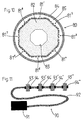
- Fig. 10 shows in a cross section schematically a cylindrical lighting device 80 according to the invention with a circular housing 84.
- the lighting device 80 comprises an octagonal heat sink 82 having a cavity 83 through which, for example, water in the image plane flows circularly.
- chip-on-board LED modules 81 1 - 81 8 are applied.
- the geometric arrangement of modules and the achievable by COB technology small distance between adjacent LED chips adjacent chip-on-board LED modules 81 1 - 81 8 allows a good overlap of the emission cone of the LEDs and thus at short intervals from the radiating Surface a good in the direction of rotation homogeneous radiation.
- the light source is surrounded by a cylindrical protective glass 84.
- the geometry of the illumination device 80 and the arrangement of the LEDs on the chip-on-board LED modules 81 1 - 81 8 is adapted to a cylindrical hollow body whose inner wall can be homogeneously irradiated by the source in their vicinity. Such a light source is needed eg in the sewer rehabilitation.
- FIG. 11 a modular construction of an exemplary lighting unit 90 according to the invention is shown.
- the illumination unit 90 comprises four cylindrical adapted illumination devices 93 - 93 "'of the invention, which, like the illumination device 80 in FIG Fig. 10 be educated.
- a lighting device 93 - 93 "'comprises at least one substrate with one or more LEDs, which is applied to a body, which may be a heat sink.
- the cooling process may include convection cooling with gases, liquid cooling or conduction (line) cooling.
- the heat sink can be produced, for example, by means of milling, punching, cutting, folding, etching, eutectic bonding of metals, etc.
- the lighting devices can be incorporated into a housing.
- 90 sensors for, for example, temperature, illuminance, current, voltage can be integrated in the lighting unit, which report the operating status to a control and supply unit 91 and allow adjustment of the operating conditions.
- the terminal units 94-94 "'allow a modular extension with respect to the number of lighting devices 93-93", as well as an interchangeability for maintenance purposes.
- the lighting devices 93-93 "'can be coupled via rigid or flexible connection units 94-94" so that they are either rigidly aligned or flexibly by means of a protective tube, metal springs or the like, so that the light source can be dragged in a tube in an arc-like manner can.
- a flexible or rigid supply line 92 connects the lighting devices 94-94 '' to the control and supply unit 91, which may include the electrical supply and the supply of cooling media, and allows targeted control of relevant operating parameters.
- Fig. 12 the result of a measurement of the radiation properties with respect to power and homogeneity of a lighting device according to the invention is shown.
- the lighting device is an elongated, in cross-section octagonal lighting device with circumferentially regularly distributed chip-on-board LED modules.
- the measurement was carried out using a tube with 14 cm tube diameter, wherein the distance of the lamp to the tube inner wall was about 1.75 cm. Irradiance levels of up to> 1 W / cm 2 were achieved.
- the total number of LED chips on the lighting devices 93-93 "'exceeds 300.
- the coordinate system in Fig. 12 is a polar coordinate system.
- the angle running from 0 ° to 360 ° describes the circumferential direction of the measurement around the illumination device, the radial coordinate the intensity in arbitrary units.
- a luminous intensity 101 averaged over the circumference is shown in dashed lines, the actual measured values of the luminous intensity 100 are connected by solid lines.
- the measurement shows that the homogeneity of the lighting device in the direction of rotation with a pipe diameter of 14 cm can be better than ⁇ 5%.
Landscapes
- Engineering & Computer Science (AREA)
- General Engineering & Computer Science (AREA)
- Microelectronics & Electronic Packaging (AREA)
- Physics & Mathematics (AREA)
- Optics & Photonics (AREA)
- Non-Portable Lighting Devices Or Systems Thereof (AREA)
- Arrangement Of Elements, Cooling, Sealing, Or The Like Of Lighting Devices (AREA)
- Fastening Of Light Sources Or Lamp Holders (AREA)
- Led Device Packages (AREA)
Priority Applications (1)
| Application Number | Priority Date | Filing Date | Title |
|---|---|---|---|
| SI201130829A SI2553314T1 (sl) | 2010-03-29 | 2011-03-25 | Svetilka LED za homogeno osvetlitev votlih teles |
Applications Claiming Priority (2)
| Application Number | Priority Date | Filing Date | Title |
|---|---|---|---|
| DE102010013286A DE102010013286B4 (de) | 2010-03-29 | 2010-03-29 | LED-Lampe zur homogenen Ausleuchtung von Hohlkörpern |
| PCT/EP2011/001510 WO2011124331A1 (de) | 2010-03-29 | 2011-03-25 | Led-lampe zur homogenen ausleuchtung von hohlkörpern |
Publications (2)
| Publication Number | Publication Date |
|---|---|
| EP2553314A1 EP2553314A1 (de) | 2013-02-06 |
| EP2553314B1 true EP2553314B1 (de) | 2016-02-24 |
Family
ID=44262814
Family Applications (1)
| Application Number | Title | Priority Date | Filing Date |
|---|---|---|---|
| EP11713180.5A Active EP2553314B1 (de) | 2010-03-29 | 2011-03-25 | Led-lampe zur homogenen ausleuchtung von hohlkörpern |
Country Status (14)
| Country | Link |
|---|---|
| US (1) | US9188289B2 (https=) |
| EP (1) | EP2553314B1 (https=) |
| JP (1) | JP5506999B2 (https=) |
| KR (1) | KR101389223B1 (https=) |
| CN (2) | CN107101091A (https=) |
| BR (1) | BR112012024455A2 (https=) |
| CA (1) | CA2792814C (https=) |
| DE (1) | DE102010013286B4 (https=) |
| ES (1) | ES2567180T3 (https=) |
| HU (1) | HUE027957T2 (https=) |
| PL (1) | PL2553314T3 (https=) |
| SI (1) | SI2553314T1 (https=) |
| TW (1) | TWI499736B (https=) |
| WO (1) | WO2011124331A1 (https=) |
Families Citing this family (51)
| Publication number | Priority date | Publication date | Assignee | Title |
|---|---|---|---|---|
| DE102011107895B4 (de) | 2011-07-18 | 2020-11-05 | Heraeus Noblelight Gmbh | Optoelektronisches Modul mit Linsensystem |
| JP5762334B2 (ja) * | 2012-02-20 | 2015-08-12 | シャープ株式会社 | 照明装置 |
| JP6133017B2 (ja) * | 2012-04-27 | 2017-05-24 | 京セラメディカル株式会社 | 膜製造装置及び人工関節コンポーネントの製造方法 |
| DE102012008638A1 (de) * | 2012-05-02 | 2013-11-07 | Heraeus Noblelight Gmbh | Leuchte mit LEDs und Zylinderlinse |
| TWI505440B (zh) * | 2012-06-04 | 2015-10-21 | 隆達電子股份有限公司 | 光源模組 |
| US8974077B2 (en) | 2012-07-30 | 2015-03-10 | Ultravision Technologies, Llc | Heat sink for LED light source |
| JP5591305B2 (ja) * | 2012-10-30 | 2014-09-17 | 株式会社トクヤマ | 紫外線発光モジュール及び紫外線照射装置 |
| USD706960S1 (en) | 2013-02-19 | 2014-06-10 | NanoGrid Limited Hong Kong | LED bulb |
| CN104075142A (zh) | 2013-03-26 | 2014-10-01 | 纳米格有限公司 | Led灯 |
| JP6075542B2 (ja) * | 2013-02-20 | 2017-02-08 | 東芝ライテック株式会社 | 発光装置および照明装置 |
| US8974078B2 (en) * | 2013-04-03 | 2015-03-10 | Litatek Corporation | Lamp with enhanced lighting angle |
| TWI550231B (zh) * | 2013-08-19 | 2016-09-21 | de-long Chen | Lamps and their flexible conductive devices |
| KR102302122B1 (ko) * | 2013-09-11 | 2021-09-13 | 헤라우스 노블라이트 아메리카 엘엘씨 | 많은 작은 방사체들을 가진 대면적 높은-균일성 uv 소스 |
| CN104576876B (zh) * | 2013-10-28 | 2017-10-31 | 四川新力光源股份有限公司 | 一体型圆锥cob封装led光源及其制备方法 |
| TW201525357A (zh) * | 2013-12-23 | 2015-07-01 | Skynet Electronic Co Ltd | 具中軸雙向對流式散熱結構之發光二極體燈泡 |
| US9195281B2 (en) | 2013-12-31 | 2015-11-24 | Ultravision Technologies, Llc | System and method for a modular multi-panel display |
| US20170136275A1 (en) * | 2014-06-23 | 2017-05-18 | Urbansite Verwaltungs Gmbh I.G. | Device, method for advertising, method for retrofitting a device, construction set and arrangement |
| CN104154455B (zh) * | 2014-07-17 | 2017-03-15 | 江苏银晶光电科技发展有限公司 | Led反应灯及使用其的光氯化反应釜 |
| USD742559S1 (en) * | 2014-10-24 | 2015-11-03 | Henry Gze Hin Chow | LED bulb |
| US9467190B1 (en) * | 2015-04-23 | 2016-10-11 | Connor Sport Court International, Llc | Mobile electronic device covering |
| US10918747B2 (en) | 2015-07-30 | 2021-02-16 | Vital Vio, Inc. | Disinfecting lighting device |
| US9927097B2 (en) | 2015-07-30 | 2018-03-27 | Vital Vio Inc. | Single diode disinfection |
| DE102015117206A1 (de) * | 2015-10-08 | 2017-04-13 | I.S.T. Innovative Sewer Technologies Gmbh | Aushärtevorrichtung mit einer UV-Licht erzeugenden Lampe |
| WO2018019655A1 (en) * | 2016-07-26 | 2018-02-01 | Philips Lighting Holding B.V. | A light emitting device |
| EP3321554B1 (en) * | 2016-10-18 | 2020-04-01 | Bolonia Servicios e Ingenieros, S.L. | A device for curing inner lining of a pipeline |
| US20180185533A1 (en) | 2016-12-29 | 2018-07-05 | Vital Vio, Inc. | Control systems for disinfecting light systems and methods of regulating operations of disinfecting light systems |
| DK3345740T3 (da) * | 2017-01-09 | 2019-07-29 | Bolonia Servicios E Ingenieros S L | Anordning til hærdning af indre harpiksrørledningsforinger |
| US11118716B2 (en) | 2017-03-03 | 2021-09-14 | Ina Acquisition Corp. | Curing device for curing a pipe liner |
| CN106647192A (zh) * | 2017-03-10 | 2017-05-10 | 深圳市华星光电技术有限公司 | 曝光设备 |
| DE102017107977A1 (de) * | 2017-04-12 | 2018-10-18 | Bernd-Jan Krasowski | Vorrichtung zum Sanieren einer Rohrleitung mittels eines Auskleide-Faserschlauchs |
| US10700252B2 (en) * | 2017-04-18 | 2020-06-30 | Bridgelux Chongqing Co., Ltd. | System and method of manufacture for LED packages |
| RU2656604C1 (ru) * | 2017-07-26 | 2018-06-06 | Федеральное государственное бюджетное учреждение науки Физический институт им. П.Н. Лебедева Российской академии наук (ФГБУН ФИАН) | Осветительный прибор |
| US11674628B2 (en) | 2017-08-18 | 2023-06-13 | Moray Group, Llc | Method, apparatus and system for lining conduits |
| US10835627B2 (en) * | 2017-12-01 | 2020-11-17 | Vital Vio, Inc. | Devices using flexible light emitting layer for creating disinfecting illuminated surface, and related method |
| US10309614B1 (en) | 2017-12-05 | 2019-06-04 | Vital Vivo, Inc. | Light directing element |
| US10413626B1 (en) | 2018-03-29 | 2019-09-17 | Vital Vio, Inc. | Multiple light emitter for inactivating microorganisms |
| RU189452U1 (ru) * | 2018-10-17 | 2019-05-22 | Закрытое акционерное общество "БТМ" | Светодиодный светильник |
| US12194168B2 (en) | 2018-12-19 | 2025-01-14 | Vyv, Inc. | Lighting and dissipation device |
| EP3690299B1 (en) * | 2019-02-04 | 2022-11-16 | Picote Solutions Inc. | Device for curing coating substance |
| US11639897B2 (en) | 2019-03-29 | 2023-05-02 | Vyv, Inc. | Contamination load sensing device |
| US11541135B2 (en) | 2019-06-28 | 2023-01-03 | Vyv, Inc. | Multiple band visible light disinfection |
| US11369704B2 (en) | 2019-08-15 | 2022-06-28 | Vyv, Inc. | Devices configured to disinfect interiors |
| EP3795880A1 (en) * | 2019-09-17 | 2021-03-24 | Sewertronics Sp. z o.o. | A device for curing pipeline inner resin linings |
| US11878084B2 (en) | 2019-09-20 | 2024-01-23 | Vyv, Inc. | Disinfecting light emitting subcomponent |
| WO2021065203A1 (ja) * | 2019-10-04 | 2021-04-08 | 東京エレクトロン株式会社 | 加熱冷却装置及び加熱冷却方法 |
| CN114999316B (zh) * | 2021-03-01 | 2024-11-26 | 南京瀚宇彩欣科技有限责任公司 | 像素结构以及可挠式显示装置 |
| RU209306U1 (ru) * | 2021-07-29 | 2022-03-15 | Марат Габдулгазизович Бикмуллин | Светильник с водяным охлаждением |
| US11906133B2 (en) | 2022-03-31 | 2024-02-20 | Alliance Sports Group, L.P. | Outdoor lighting apparatus |
| KR102851401B1 (ko) * | 2022-11-30 | 2025-09-01 | 유버 주식회사 | Led모듈 및 이를 사용하는 노광장치 |
| SE547538C2 (en) * | 2024-05-10 | 2025-10-14 | Peanta Invent Ab | Light head for use in relining pipes |
| JP7829197B1 (ja) * | 2025-07-02 | 2026-03-13 | 株式会社環境施設 | 光照射装置および光照射システム |
Family Cites Families (29)
| Publication number | Priority date | Publication date | Assignee | Title |
|---|---|---|---|---|
| DE69936375T2 (de) * | 1998-09-17 | 2008-02-28 | Koninklijke Philips Electronics N.V. | Led-leuchte |
| JP2002184207A (ja) * | 2000-12-15 | 2002-06-28 | Matsushita Electric Ind Co Ltd | Led照明用電球 |
| JP3851174B2 (ja) * | 2001-01-25 | 2006-11-29 | 松下電器産業株式会社 | 発光ユニット、発光ユニット組合せ体、および照明装置 |
| JP2007059930A (ja) | 2001-08-09 | 2007-03-08 | Matsushita Electric Ind Co Ltd | Led照明装置およびカード型led照明光源 |
| US7781787B2 (en) * | 2001-11-16 | 2010-08-24 | Toyoda Gosei, Co., Ltd. | Light-emitting diode, led light, and light apparatus |
| US7093958B2 (en) * | 2002-04-09 | 2006-08-22 | Osram Sylvania Inc. | LED light source assembly |
| CN100547282C (zh) * | 2002-04-25 | 2009-10-07 | 林原 | 可挠性发光体装置及其制造方法 |
| US20030235800A1 (en) * | 2002-06-24 | 2003-12-25 | Qadar Steven Abdel | LED curing light |
| US20050169006A1 (en) * | 2004-01-30 | 2005-08-04 | Harvatek Corporation | Led chip lamp apparatus |
| US7070311B2 (en) * | 2004-06-03 | 2006-07-04 | Fu An Industrial Co., Ltd. | Vehicle light for producing light whose form depends on orientations of plural refraction elements |
| US7829899B2 (en) * | 2006-05-03 | 2010-11-09 | Cree, Inc. | Multi-element LED lamp package |
| CN101126485A (zh) * | 2006-08-18 | 2008-02-20 | 蒋承庭 | 具发光二极管的光源模块及其形成方法 |
| JP2008142996A (ja) * | 2006-12-08 | 2008-06-26 | S G C Gesuido Center Kk | 配管のライニング方法および光硬化装置 |
| JP2008175381A (ja) | 2007-01-18 | 2008-07-31 | Bkp Berolina Polyester Gmbh & Co Kg | Ledを備えた硬化更生装置 |
| EP1959183A1 (en) * | 2007-02-19 | 2008-08-20 | Per Aarsleff A/S | An apparatus and a method for curing a liner of a pipeline |
| JP4964015B2 (ja) | 2007-04-24 | 2012-06-27 | 吉佳株式会社 | 光硬化性ライニング材の光硬化方法及び該方法に用いる光硬化システム |
| JP2008277174A (ja) | 2007-04-27 | 2008-11-13 | Litehouse Technologies Corp | 発光装置及び装着用フレーム |
| RU2475674C2 (ru) | 2007-05-02 | 2013-02-20 | Конинклейке Филипс Электроникс Н.В. | Твердотельное устройство освещения |
| US7744250B2 (en) * | 2007-07-12 | 2010-06-29 | Fu Zhun Precision Industry (Shen Zhen) Co., Ltd. | LED lamp with a heat dissipation device |
| DE102007038197A1 (de) * | 2007-08-14 | 2009-02-19 | Brandenburger Patentverwertung GbR (vertretungsberechtigter Gesellschafter: Wilhelm Leo Betz, 76887 Bad Bergzabern) | Verfahren und Vorrichtung zum Sanieren von Rohrleitungen |
| DE102007038196A1 (de) * | 2007-08-14 | 2009-02-19 | Brandenburger Patentverwertung GbR (vertretungsberechtigter Gesellschafter: Wilhelm Leo Betz, 76887 Bad Bergzabern) | Verfahren zum Sanieren von Abzweigleitungen in Kanalrohren |
| KR20090006121U (ko) * | 2007-12-17 | 2009-06-22 | 추 야오 우 | 발광 다이오드 램프 |
| DE102008010167B4 (de) * | 2008-02-20 | 2018-10-25 | Brandenburger Patentverwertung GbR (vertretungsberechtigter Gesellschafter: Tim Brandenburger, 76829 Landau) | Vorrichtung und Verfahren zum Härten von harzgetränkten Faserschläuchen |
| US20100001664A1 (en) * | 2008-02-26 | 2010-01-07 | Shu-Chuan Shih | Illuminating fabric product |
| JP2009277586A (ja) * | 2008-05-16 | 2009-11-26 | San Corporation Kk | 電球型led照明器具 |
| AT524690B1 (de) * | 2008-07-24 | 2022-08-15 | Tridonic Gmbh & Co Kg | Leuchtmittel mit led |
| EP2151617A1 (en) * | 2008-08-05 | 2010-02-10 | Per Aarsleff A/S | Pipeline sealing apparatus, method of sealing a pipeline and a sealing system |
| JP2010055993A (ja) | 2008-08-29 | 2010-03-11 | Toshiba Lighting & Technology Corp | 照明装置および照明器具 |
| US8342733B2 (en) * | 2009-12-14 | 2013-01-01 | Tyco Electronics Corporation | LED lighting assemblies |
-
2010
- 2010-03-29 DE DE102010013286A patent/DE102010013286B4/de active Active
-
2011
- 2011-03-25 CA CA2792814A patent/CA2792814C/en active Active
- 2011-03-25 BR BR112012024455A patent/BR112012024455A2/pt not_active Application Discontinuation
- 2011-03-25 KR KR1020127025811A patent/KR101389223B1/ko active Active
- 2011-03-25 JP JP2013501676A patent/JP5506999B2/ja active Active
- 2011-03-25 WO PCT/EP2011/001510 patent/WO2011124331A1/de not_active Ceased
- 2011-03-25 EP EP11713180.5A patent/EP2553314B1/de active Active
- 2011-03-25 HU HUE11713180A patent/HUE027957T2/en unknown
- 2011-03-25 CN CN201611014782.XA patent/CN107101091A/zh active Pending
- 2011-03-25 ES ES11713180.5T patent/ES2567180T3/es active Active
- 2011-03-25 PL PL11713180.5T patent/PL2553314T3/pl unknown
- 2011-03-25 CN CN2011800168863A patent/CN102812285A/zh active Pending
- 2011-03-25 US US13/637,661 patent/US9188289B2/en active Active
- 2011-03-25 SI SI201130829A patent/SI2553314T1/sl unknown
- 2011-03-29 TW TW100110848A patent/TWI499736B/zh not_active IP Right Cessation
Also Published As
| Publication number | Publication date |
|---|---|
| DE102010013286A1 (de) | 2011-09-29 |
| TW201202601A (en) | 2012-01-16 |
| TWI499736B (zh) | 2015-09-11 |
| KR101389223B1 (ko) | 2014-04-24 |
| SI2553314T1 (sl) | 2016-06-30 |
| US20130010460A1 (en) | 2013-01-10 |
| PL2553314T3 (pl) | 2016-09-30 |
| DE102010013286B4 (de) | 2012-03-22 |
| CN102812285A (zh) | 2012-12-05 |
| ES2567180T3 (es) | 2016-04-20 |
| CA2792814C (en) | 2015-02-17 |
| JP5506999B2 (ja) | 2014-05-28 |
| EP2553314A1 (de) | 2013-02-06 |
| CA2792814A1 (en) | 2011-10-13 |
| JP2013524415A (ja) | 2013-06-17 |
| HUE027957T2 (en) | 2016-11-28 |
| CN107101091A (zh) | 2017-08-29 |
| KR20120138795A (ko) | 2012-12-26 |
| WO2011124331A1 (de) | 2011-10-13 |
| BR112012024455A2 (pt) | 2016-05-31 |
| US9188289B2 (en) | 2015-11-17 |
Similar Documents
| Publication | Publication Date | Title |
|---|---|---|
| EP2553314B1 (de) | Led-lampe zur homogenen ausleuchtung von hohlkörpern | |
| DE102011107895B4 (de) | Optoelektronisches Modul mit Linsensystem | |
| EP2614694B1 (de) | Beschichtungsverfahren für ein optoelektronisches chip-on-board-modul | |
| EP2459924B1 (de) | Beleuchtungsvorrichtung mit leuchtdioden | |
| EP3396713B1 (de) | Leuchte mit leds und zylinderlinse | |
| EP1528388B1 (de) | UV-Lichtemissionsdioden als Strahlungsquelle einer Vorrichtung zur künstlichen Bewitterung von Proben | |
| DE102011107893A1 (de) | Optoelektronisches Modul mit verbesserter Optik | |
| WO2014090693A1 (de) | Bestrahlungsvorrichtung zur bestrahlung von pflanzen | |
| EP2488787A1 (de) | Leuchtmodul | |
| DE212013000099U1 (de) | Lineare Fresneloptik zum Reduzieren der Winkeldispersion von Licht von einer LED-Anordnung | |
| DE102018222307A1 (de) | Vorrichtung und Verfahren zum Entkeimen eines durchfliessenden Fluids | |
| DE102018123971B4 (de) | LED-Lampe | |
| DE102011107892A1 (de) | Beschichtungsverfahren für einoptoelektronisches Chip-On-Board-Modul | |
| DE212013000056U1 (de) | Randgewichteter Abstand von LEDS für Bereich verbesserter Gleichmässigkeit | |
| EP2326962B1 (de) | Vorrichtung zum prüfen von solarzellen | |
| EP3190617A1 (de) | Lichtemittierende baugruppe und verfahren zum herstellen einer lichtemittierenden baugruppe | |
| DE102008031930B4 (de) | Beleuchtungsvorrichtung mit Mikro-Linsenarray | |
| EP2748515B1 (de) | Lichtquellenvorrichtung | |
| DE102016224341A1 (de) | Scheinwerfer und Basisscheinwerfermodul für einen Scheinwerfer | |
| DE102014100141B4 (de) | Bestrahlungsvorrichtung zur Bestrahlung von Pflanzen | |
| DE202015007511U1 (de) | LED-Lampe |
Legal Events
| Date | Code | Title | Description |
|---|---|---|---|
| PUAI | Public reference made under article 153(3) epc to a published international application that has entered the european phase |
Free format text: ORIGINAL CODE: 0009012 |
|
| 17P | Request for examination filed |
Effective date: 20120830 |
|
| AK | Designated contracting states |
Kind code of ref document: A1 Designated state(s): AL AT BE BG CH CY CZ DE DK EE ES FI FR GB GR HR HU IE IS IT LI LT LU LV MC MK MT NL NO PL PT RO RS SE SI SK SM TR |
|
| DAX | Request for extension of the european patent (deleted) | ||
| 17Q | First examination report despatched |
Effective date: 20150113 |
|
| GRAP | Despatch of communication of intention to grant a patent |
Free format text: ORIGINAL CODE: EPIDOSNIGR1 |
|
| RIC1 | Information provided on ipc code assigned before grant |
Ipc: F21K 99/00 20100101AFI20150831BHEP Ipc: F21Y 111/00 20060101ALN20150831BHEP Ipc: F21Y 101/02 20060101ALN20150831BHEP |
|
| RIC1 | Information provided on ipc code assigned before grant |
Ipc: F21Y 101/02 20060101ALN20150911BHEP Ipc: F21Y 111/00 20060101ALN20150911BHEP Ipc: F21K 99/00 20100101AFI20150911BHEP |
|
| INTG | Intention to grant announced |
Effective date: 20151007 |
|
| GRAS | Grant fee paid |
Free format text: ORIGINAL CODE: EPIDOSNIGR3 |
|
| RIC1 | Information provided on ipc code assigned before grant |
Ipc: F21K 99/00 20160101AFI20151216BHEP Ipc: F21Y 111/00 20160101ALN20151216BHEP |
|
| GRAA | (expected) grant |
Free format text: ORIGINAL CODE: 0009210 |
|
| AK | Designated contracting states |
Kind code of ref document: B1 Designated state(s): AL AT BE BG CH CY CZ DE DK EE ES FI FR GB GR HR HU IE IS IT LI LT LU LV MC MK MT NL NO PL PT RO RS SE SI SK SM TR |
|
| REG | Reference to a national code |
Ref country code: GB Ref legal event code: FG4D Free format text: NOT ENGLISH |
|
| REG | Reference to a national code |
Ref country code: CH Ref legal event code: EP |
|
| REG | Reference to a national code |
Ref country code: AT Ref legal event code: REF Ref document number: 776916 Country of ref document: AT Kind code of ref document: T Effective date: 20160315 |
|
| REG | Reference to a national code |
Ref country code: FR Ref legal event code: PLFP Year of fee payment: 6 |
|
| REG | Reference to a national code |
Ref country code: IE Ref legal event code: FG4D Free format text: LANGUAGE OF EP DOCUMENT: GERMAN |
|
| REG | Reference to a national code |
Ref country code: DE Ref legal event code: R096 Ref document number: 502011008915 Country of ref document: DE |
|
| REG | Reference to a national code |
Ref country code: PT Ref legal event code: SC4A Free format text: AVAILABILITY OF NATIONAL TRANSLATION Effective date: 20160406 |
|
| REG | Reference to a national code |
Ref country code: ES Ref legal event code: FG2A Ref document number: 2567180 Country of ref document: ES Kind code of ref document: T3 Effective date: 20160420 |
|
| REG | Reference to a national code |
Ref country code: RO Ref legal event code: EPE |
|
| REG | Reference to a national code |
Ref country code: NL Ref legal event code: FP |
|
| REG | Reference to a national code |
Ref country code: SE Ref legal event code: TRGR |
|
| REG | Reference to a national code |
Ref country code: NO Ref legal event code: T2 Effective date: 20160224 |
|
| REG | Reference to a national code |
Ref country code: EE Ref legal event code: FG4A Ref document number: E011977 Country of ref document: EE Effective date: 20160518 Ref country code: GR Ref legal event code: EP Ref document number: 20160400591 Country of ref document: GR Effective date: 20160505 |
|
| PG25 | Lapsed in a contracting state [announced via postgrant information from national office to epo] |
Ref country code: HR Free format text: LAPSE BECAUSE OF FAILURE TO SUBMIT A TRANSLATION OF THE DESCRIPTION OR TO PAY THE FEE WITHIN THE PRESCRIBED TIME-LIMIT Effective date: 20160224 |
|
| PG25 | Lapsed in a contracting state [announced via postgrant information from national office to epo] |
Ref country code: RS Free format text: LAPSE BECAUSE OF FAILURE TO SUBMIT A TRANSLATION OF THE DESCRIPTION OR TO PAY THE FEE WITHIN THE PRESCRIBED TIME-LIMIT Effective date: 20160224 |
|
| REG | Reference to a national code |
Ref country code: SK Ref legal event code: T3 Ref document number: E 21062 Country of ref document: SK |
|
| PG25 | Lapsed in a contracting state [announced via postgrant information from national office to epo] |
Ref country code: DK Free format text: LAPSE BECAUSE OF FAILURE TO SUBMIT A TRANSLATION OF THE DESCRIPTION OR TO PAY THE FEE WITHIN THE PRESCRIBED TIME-LIMIT Effective date: 20160224 |
|
| REG | Reference to a national code |
Ref country code: DE Ref legal event code: R097 Ref document number: 502011008915 Country of ref document: DE |
|
| REG | Reference to a national code |
Ref country code: HU Ref legal event code: AG4A Ref document number: E027957 Country of ref document: HU |
|
| PG25 | Lapsed in a contracting state [announced via postgrant information from national office to epo] |
Ref country code: SM Free format text: LAPSE BECAUSE OF FAILURE TO SUBMIT A TRANSLATION OF THE DESCRIPTION OR TO PAY THE FEE WITHIN THE PRESCRIBED TIME-LIMIT Effective date: 20160224 |
|
| PLBE | No opposition filed within time limit |
Free format text: ORIGINAL CODE: 0009261 |
|
| STAA | Information on the status of an ep patent application or granted ep patent |
Free format text: STATUS: NO OPPOSITION FILED WITHIN TIME LIMIT |
|
| 26N | No opposition filed |
Effective date: 20161125 |
|
| REG | Reference to a national code |
Ref country code: FR Ref legal event code: PLFP Year of fee payment: 7 |
|
| PG25 | Lapsed in a contracting state [announced via postgrant information from national office to epo] |
Ref country code: MT Free format text: LAPSE BECAUSE OF FAILURE TO SUBMIT A TRANSLATION OF THE DESCRIPTION OR TO PAY THE FEE WITHIN THE PRESCRIBED TIME-LIMIT Effective date: 20160224 |
|
| REG | Reference to a national code |
Ref country code: HU Ref legal event code: HC9C Ref country code: FR Ref legal event code: PLFP Year of fee payment: 8 |
|
| PG25 | Lapsed in a contracting state [announced via postgrant information from national office to epo] |
Ref country code: CY Free format text: LAPSE BECAUSE OF FAILURE TO SUBMIT A TRANSLATION OF THE DESCRIPTION OR TO PAY THE FEE WITHIN THE PRESCRIBED TIME-LIMIT Effective date: 20160224 |
|
| PG25 | Lapsed in a contracting state [announced via postgrant information from national office to epo] |
Ref country code: MC Free format text: LAPSE BECAUSE OF FAILURE TO SUBMIT A TRANSLATION OF THE DESCRIPTION OR TO PAY THE FEE WITHIN THE PRESCRIBED TIME-LIMIT Effective date: 20160224 Ref country code: MK Free format text: LAPSE BECAUSE OF FAILURE TO SUBMIT A TRANSLATION OF THE DESCRIPTION OR TO PAY THE FEE WITHIN THE PRESCRIBED TIME-LIMIT Effective date: 20160224 Ref country code: IS Free format text: LAPSE BECAUSE OF FAILURE TO SUBMIT A TRANSLATION OF THE DESCRIPTION OR TO PAY THE FEE WITHIN THE PRESCRIBED TIME-LIMIT Effective date: 20160224 |
|
| PG25 | Lapsed in a contracting state [announced via postgrant information from national office to epo] |
Ref country code: AL Free format text: LAPSE BECAUSE OF FAILURE TO SUBMIT A TRANSLATION OF THE DESCRIPTION OR TO PAY THE FEE WITHIN THE PRESCRIBED TIME-LIMIT Effective date: 20160224 |
|
| REG | Reference to a national code |
Ref country code: DE Ref legal event code: R082 Ref document number: 502011008915 Country of ref document: DE Representative=s name: BRAND, NORMEN, DR. RER. NAT., DE Ref country code: DE Ref legal event code: R082 Ref document number: 502011008915 Country of ref document: DE Representative=s name: EULER, MATTHIAS, DR., DE Ref country code: DE Ref legal event code: R082 Ref document number: 502011008915 Country of ref document: DE Representative=s name: BRAND, NORMEN, DIPL.-CHEM. UNIV. DR. RER. NAT., DE |
|
| PGFP | Annual fee paid to national office [announced via postgrant information from national office to epo] |
Ref country code: SI Payment date: 20190206 Year of fee payment: 13 Ref country code: IE Payment date: 20190322 Year of fee payment: 9 Ref country code: BG Payment date: 20190321 Year of fee payment: 9 Ref country code: NO Payment date: 20190325 Year of fee payment: 9 Ref country code: LT Payment date: 20190219 Year of fee payment: 9 Ref country code: RO Payment date: 20190225 Year of fee payment: 9 Ref country code: CH Payment date: 20190320 Year of fee payment: 9 Ref country code: FI Payment date: 20190321 Year of fee payment: 9 |
|
| PGFP | Annual fee paid to national office [announced via postgrant information from national office to epo] |
Ref country code: HU Payment date: 20190314 Year of fee payment: 9 Ref country code: AT Payment date: 20190321 Year of fee payment: 9 Ref country code: LV Payment date: 20190312 Year of fee payment: 9 Ref country code: GR Payment date: 20190313 Year of fee payment: 9 Ref country code: TR Payment date: 20190320 Year of fee payment: 9 Ref country code: EE Payment date: 20190318 Year of fee payment: 9 Ref country code: SE Payment date: 20190320 Year of fee payment: 9 |
|
| PGFP | Annual fee paid to national office [announced via postgrant information from national office to epo] |
Ref country code: SK Payment date: 20190227 Year of fee payment: 9 |
|
| PGFP | Annual fee paid to national office [announced via postgrant information from national office to epo] |
Ref country code: PT Payment date: 20190225 Year of fee payment: 9 Ref country code: ES Payment date: 20190418 Year of fee payment: 9 |
|
| REG | Reference to a national code |
Ref country code: DE Ref legal event code: R082 Ref document number: 502011008915 Country of ref document: DE Representative=s name: BRAND, NORMEN, DR. RER. NAT., DE Ref country code: DE Ref legal event code: R082 Ref document number: 502011008915 Country of ref document: DE Representative=s name: BRAND, NORMEN, DIPL.-CHEM. UNIV. DR. RER. NAT., DE |
|
| REG | Reference to a national code |
Ref country code: FI Ref legal event code: MAE |
|
| REG | Reference to a national code |
Ref country code: EE Ref legal event code: MM4A Ref document number: E011977 Country of ref document: EE Effective date: 20200331 |
|
| REG | Reference to a national code |
Ref country code: NO Ref legal event code: MMEP |
|
| PG25 | Lapsed in a contracting state [announced via postgrant information from national office to epo] |
Ref country code: FI Free format text: LAPSE BECAUSE OF NON-PAYMENT OF DUE FEES Effective date: 20200325 Ref country code: RO Free format text: LAPSE BECAUSE OF NON-PAYMENT OF DUE FEES Effective date: 20200325 Ref country code: PT Free format text: LAPSE BECAUSE OF NON-PAYMENT OF DUE FEES Effective date: 20200925 Ref country code: CZ Free format text: LAPSE BECAUSE OF NON-PAYMENT OF DUE FEES Effective date: 20200325 |
|
| REG | Reference to a national code |
Ref country code: CH Ref legal event code: PL |
|
| REG | Reference to a national code |
Ref country code: AT Ref legal event code: MM01 Ref document number: 776916 Country of ref document: AT Kind code of ref document: T Effective date: 20200325 |
|
| PG25 | Lapsed in a contracting state [announced via postgrant information from national office to epo] |
Ref country code: LV Free format text: LAPSE BECAUSE OF NON-PAYMENT OF DUE FEES Effective date: 20200325 |
|
| REG | Reference to a national code |
Ref country code: SK Ref legal event code: MM4A Ref document number: E 21062 Country of ref document: SK Effective date: 20200325 |
|
| REG | Reference to a national code |
Ref country code: BE Ref legal event code: MM Effective date: 20200331 |
|
| REG | Reference to a national code |
Ref country code: LT Ref legal event code: MM4D Effective date: 20200325 |
|
| PG25 | Lapsed in a contracting state [announced via postgrant information from national office to epo] |
Ref country code: LU Free format text: LAPSE BECAUSE OF NON-PAYMENT OF DUE FEES Effective date: 20200325 |
|
| REG | Reference to a national code |
Ref country code: SI Ref legal event code: KO00 Effective date: 20201113 |
|
| PG25 | Lapsed in a contracting state [announced via postgrant information from national office to epo] |
Ref country code: SE Free format text: LAPSE BECAUSE OF NON-PAYMENT OF DUE FEES Effective date: 20200326 Ref country code: GR Free format text: LAPSE BECAUSE OF NON-PAYMENT OF DUE FEES Effective date: 20201008 Ref country code: EE Free format text: LAPSE BECAUSE OF NON-PAYMENT OF DUE FEES Effective date: 20200331 Ref country code: HU Free format text: LAPSE BECAUSE OF NON-PAYMENT OF DUE FEES Effective date: 20200326 Ref country code: NO Free format text: LAPSE BECAUSE OF NON-PAYMENT OF DUE FEES Effective date: 20200331 Ref country code: LI Free format text: LAPSE BECAUSE OF NON-PAYMENT OF DUE FEES Effective date: 20200331 Ref country code: BG Free format text: LAPSE BECAUSE OF NON-PAYMENT OF DUE FEES Effective date: 20201130 Ref country code: CH Free format text: LAPSE BECAUSE OF NON-PAYMENT OF DUE FEES Effective date: 20200331 Ref country code: LT Free format text: LAPSE BECAUSE OF NON-PAYMENT OF DUE FEES Effective date: 20200325 Ref country code: AT Free format text: LAPSE BECAUSE OF NON-PAYMENT OF DUE FEES Effective date: 20200325 Ref country code: IE Free format text: LAPSE BECAUSE OF NON-PAYMENT OF DUE FEES Effective date: 20200325 |
|
| PG25 | Lapsed in a contracting state [announced via postgrant information from national office to epo] |
Ref country code: SI Free format text: LAPSE BECAUSE OF NON-PAYMENT OF DUE FEES Effective date: 20200326 Ref country code: BE Free format text: LAPSE BECAUSE OF NON-PAYMENT OF DUE FEES Effective date: 20200331 Ref country code: SK Free format text: LAPSE BECAUSE OF NON-PAYMENT OF DUE FEES Effective date: 20200325 |
|
| REG | Reference to a national code |
Ref country code: ES Ref legal event code: FD2A Effective date: 20210806 |
|
| PG25 | Lapsed in a contracting state [announced via postgrant information from national office to epo] |
Ref country code: ES Free format text: LAPSE BECAUSE OF NON-PAYMENT OF DUE FEES Effective date: 20200326 |
|
| PG25 | Lapsed in a contracting state [announced via postgrant information from national office to epo] |
Ref country code: TR Free format text: LAPSE BECAUSE OF NON-PAYMENT OF DUE FEES Effective date: 20200325 |
|
| PGFP | Annual fee paid to national office [announced via postgrant information from national office to epo] |
Ref country code: PL Payment date: 20230321 Year of fee payment: 13 |
|
| PGFP | Annual fee paid to national office [announced via postgrant information from national office to epo] |
Ref country code: NL Payment date: 20230321 Year of fee payment: 13 |
|
| P01 | Opt-out of the competence of the unified patent court (upc) registered |
Effective date: 20230530 |
|
| PGFP | Annual fee paid to national office [announced via postgrant information from national office to epo] |
Ref country code: IT Payment date: 20230328 Year of fee payment: 13 |
|
| REG | Reference to a national code |
Ref country code: DE Ref legal event code: R082 Ref document number: 502011008915 Country of ref document: DE Representative=s name: MEWBURN ELLIS LLP, DE |
|
| REG | Reference to a national code |
Ref country code: NL Ref legal event code: MM Effective date: 20240401 |
|
| PG25 | Lapsed in a contracting state [announced via postgrant information from national office to epo] |
Ref country code: NL Free format text: LAPSE BECAUSE OF NON-PAYMENT OF DUE FEES Effective date: 20240401 |
|
| PG25 | Lapsed in a contracting state [announced via postgrant information from national office to epo] |
Ref country code: NL Free format text: LAPSE BECAUSE OF NON-PAYMENT OF DUE FEES Effective date: 20240401 |
|
| PGFP | Annual fee paid to national office [announced via postgrant information from national office to epo] |
Ref country code: DE Payment date: 20250327 Year of fee payment: 15 |
|
| PG25 | Lapsed in a contracting state [announced via postgrant information from national office to epo] |
Ref country code: PL Free format text: LAPSE BECAUSE OF NON-PAYMENT OF DUE FEES Effective date: 20240325 |
|
| PGFP | Annual fee paid to national office [announced via postgrant information from national office to epo] |
Ref country code: FR Payment date: 20250325 Year of fee payment: 15 |
|
| PG25 | Lapsed in a contracting state [announced via postgrant information from national office to epo] |
Ref country code: IT Free format text: LAPSE BECAUSE OF NON-PAYMENT OF DUE FEES Effective date: 20240325 |
|
| PGFP | Annual fee paid to national office [announced via postgrant information from national office to epo] |
Ref country code: GB Payment date: 20250327 Year of fee payment: 15 |