EP2552020A2 - Electronic device, oscillator, and method of manufacturing electronic device - Google Patents
Electronic device, oscillator, and method of manufacturing electronic device Download PDFInfo
- Publication number
- EP2552020A2 EP2552020A2 EP12168387A EP12168387A EP2552020A2 EP 2552020 A2 EP2552020 A2 EP 2552020A2 EP 12168387 A EP12168387 A EP 12168387A EP 12168387 A EP12168387 A EP 12168387A EP 2552020 A2 EP2552020 A2 EP 2552020A2
- Authority
- EP
- European Patent Office
- Prior art keywords
- base substrate
- substrate
- electronic device
- lid substrate
- lid
- Prior art date
- Legal status (The legal status is an assumption and is not a legal conclusion. Google has not performed a legal analysis and makes no representation as to the accuracy of the status listed.)
- Withdrawn
Links
Images


Classifications
-
- H—ELECTRICITY
- H03—ELECTRONIC CIRCUITRY
- H03B—GENERATION OF OSCILLATIONS, DIRECTLY OR BY FREQUENCY-CHANGING, BY CIRCUITS EMPLOYING ACTIVE ELEMENTS WHICH OPERATE IN A NON-SWITCHING MANNER; GENERATION OF NOISE BY SUCH CIRCUITS
- H03B5/00—Generation of oscillations using amplifier with regenerative feedback from output to input
- H03B5/30—Generation of oscillations using amplifier with regenerative feedback from output to input with frequency-determining element being electromechanical resonator
- H03B5/32—Generation of oscillations using amplifier with regenerative feedback from output to input with frequency-determining element being electromechanical resonator being a piezoelectric resonator
-
- H—ELECTRICITY
- H10—SEMICONDUCTOR DEVICES; ELECTRIC SOLID-STATE DEVICES NOT OTHERWISE PROVIDED FOR
- H10W—GENERIC PACKAGES, INTERCONNECTIONS, CONNECTORS OR OTHER CONSTRUCTIONAL DETAILS OF DEVICES COVERED BY CLASS H10
- H10W76/00—Containers; Fillings or auxiliary members therefor; Seals
- H10W76/10—Containers or parts thereof
- H10W76/12—Containers or parts thereof characterised by their shape
-
- H—ELECTRICITY
- H03—ELECTRONIC CIRCUITRY
- H03H—IMPEDANCE NETWORKS, e.g. RESONANT CIRCUITS; RESONATORS
- H03H9/00—Networks comprising electromechanical or electro-acoustic elements; Electromechanical resonators
- H03H9/02—Details
- H03H9/05—Holders or supports
- H03H9/10—Mounting in enclosures
- H03H9/1007—Mounting in enclosures for bulk acoustic wave [BAW] devices
- H03H9/1014—Mounting in enclosures for bulk acoustic wave [BAW] devices the enclosure being defined by a frame built on a substrate and a cap, the frame having no mechanical contact with the BAW device
- H03H9/1021—Mounting in enclosures for bulk acoustic wave [BAW] devices the enclosure being defined by a frame built on a substrate and a cap, the frame having no mechanical contact with the BAW device the BAW device being of the cantilever type
-
- H—ELECTRICITY
- H10—SEMICONDUCTOR DEVICES; ELECTRIC SOLID-STATE DEVICES NOT OTHERWISE PROVIDED FOR
- H10W—GENERIC PACKAGES, INTERCONNECTIONS, CONNECTORS OR OTHER CONSTRUCTIONAL DETAILS OF DEVICES COVERED BY CLASS H10
- H10W70/00—Package substrates; Interposers; Redistribution layers [RDL]
- H10W70/60—Insulating or insulated package substrates; Interposers; Redistribution layers
-
- Y—GENERAL TAGGING OF NEW TECHNOLOGICAL DEVELOPMENTS; GENERAL TAGGING OF CROSS-SECTIONAL TECHNOLOGIES SPANNING OVER SEVERAL SECTIONS OF THE IPC; TECHNICAL SUBJECTS COVERED BY FORMER USPC CROSS-REFERENCE ART COLLECTIONS [XRACs] AND DIGESTS
- Y10—TECHNICAL SUBJECTS COVERED BY FORMER USPC
- Y10T—TECHNICAL SUBJECTS COVERED BY FORMER US CLASSIFICATION
- Y10T29/00—Metal working
- Y10T29/49—Method of mechanical manufacture
- Y10T29/49002—Electrical device making
Definitions
- the present invention relates to an electronic device including an electronic element mounted in a cavity formed between two substrates, an oscillator, and a method of manufacturing the electronic device.
- Portable information terminals such as cellular phones widely available in recent years often employ electronic devices with small packages of a surface mount type.
- a vibrator, a MEMS, a gyrosensor, an acceleration sensor or the like has a structure in which an electronic element is housed in a package of a hollow cavity structure.
- a known example of the package of the hollow cavity type is provided by anodic-bonding a base substrate to a lid substrate with a metal film interposed between them.
- a method of the anodic bonding is described, for example in JP-A-9-2845 .
- Fig. 10 shows a method of simultaneously forming a number of electronic devices 50 of this type.
- a base substrate 51 and a lid substrate 52 are prepared.
- a plurality of through holes are formed in the base substrate 51, and a conductive material is embedded in each of the through holes to provide a through electrode 56.
- An electrode terminal 58 is formed on a back face of the base substrate 51 for electrical connection to the through electrode 56.
- a number of electronic elements 55 are mounted on a front face of the base substrate 51. In mounting of the electronic element 55, the electronic element 55 is electrically connected to the through electrode 56.
- a number of recess portions 59 are formed in the lid substrate 52. Then, the base substrate 51 is overlaid on the lid substrate 52 and they are bonded together. The bonding is performed with an adhesive or anodic bonding.
- the recess portion 59 in the lid substrate 52 provides a cavity 54, and the electronic element 55 is housed in the cavity 54. Then, the substrates are split into individual electronic devices.
- the base substrate 51 and the lid substrate 52 are deformed when the through electrodes 56 and the recess portions 59 are formed. This reduces the accuracy of the alignment of the lid substrate 52 and the base substrate 51. Warping also occurs as shown in Fig. 10 after the bonding of the base substrate 51 to the lid substrate 52.
- the substrates are significantly warped, especially when the outer diameters of the base substrate 51 and the lid substrate 52 are increased to obtain a larger number of devices, which makes it difficult to align the base substrate 51 with the lid substrate 52.
- a change in ambient temperature changes the stress applied to the mounted electronic element 55, and the stress change disadvantageously varies the characteristics of the electronic element 55.
- the invention has been made in view of the problems described above, and it is an object thereof to provide an electronic device with reduced deformation of a substrate, and a method of manufacturing the same.
- An electronic device includes a lid substrate, a base substrate bonded to the lid substrate and forming a cavity hermetically sealed from the outside air between the base substrate and the lid substrate, an electronic element housed in the cavity, and a mold member placed on an outer face of the lid substrate or the base substrate.
- the lid substrate has a recess portion and the recess portion forms the cavity.
- the base substrate has a through electrode passing from an inner face on the side of the cavity to an outer face on the side opposite to the cavity, and the electronic element is electrically connected to the through electrode.
- the lid substrate and the base substrate are bonded together with a bonding material including a metal material interposed between them.
- the electronic element is a crystal vibrator mounted in the form of a cantilever on the inner face of the base substrate.
- the mold member is formed of an epoxy resin.
- An oscillator includes the electronic device described in any of the above, and a driving circuit supplying a driving signal to the electronic device.
- a method of manufacturing an electronic device includes a recess portion forming step of forming a recess portion in a lid substrate, a mounting step of mounting an electronic element on a base substrate, a mold member placing step of placing a mold member on an outer face of the lid substrate or the base substrate, and a bonding step of bonding the lid substrate to the base substrate with the electronic element housed in the recess portion.
- the mold member placing step is performed before the bonding step.
- the mold member placing step is performed after the bonding step.
- a through electrode forming step of forming a through electrode in the base substrate is further included, and the mold member placing step is a step of placing the mold member such that the through electrode is exposed on an outer face of the base substrate on the side opposite to the side where the electronic element is mounted.
- the recess portion forming step is a step of mounting a plurality of recess portions in the lid substrate
- the mounting step is a step of mounting a plurality of the electronic elements on the base substrate.
- a splitting step of cutting and splitting a stack formed of the lid substrate and the base substrate bonded together is included.
- the electronic device includes the lid substrate, the base substrate bonded to the lid substrate and forming the cavity between the base substrate and the lid substrate, the electronic element housed in the cavity, and the mold member placed on the outer face of the lid substrate or the base substrate.
- the mold member placed on the outer face of the lid substrate or the base substrate can reduce warping of the substrate to facilitate alignment of the lid substrate and the base substrate, thereby reducing the rate of occurrence of defects.
- variations in stress applied to the electronic element from the lid substrate or the base substrate can be reduced to stabilize the characteristics of the electronic element.
- An electronic device includes a lid substrate, a base substrate bonded to the lid substrate and forming a cavity between the base substrate and the lid substrate, an electronic element housed in the cavity, and a mold member placed on an outer face of the lid substrate or the base substrate.
- the configuration of the invention can reduce warping of the lid substrate or the base substrate to facilitate the alignment of the lid substrate and the base substrate, thereby reducing the rate of occurrence of defects.
- the reduced warping of the substrate allows the use of a large glass substrate from which a number of devices can be obtained, so that the cost of the electronic device can be cut.
- the reduced warping of the substrate relieves variations in stress applied to the electronic element resulting from a change in ambient temperature, which stabilizes the characteristics of the electronic element.
- the lid substrate and the base substrate can be provided by using glass, ceramics, synthetic resin, or other materials. When a glass material is used, working thereof is easily performed and impregnation with water or other impurities can be prevented, and therefore, a package can be formed at low cost and with high reliability.
- the cavity may be formed of a recess portion formed in the lid substrate or a recess portion formed in the base substrate.
- the electronic element may be mounted on an inner face of the lid substrate or may be mounted on an inner face of the base substrate.
- the mold member may be formed on the outer face of the lid substrate, may be formed on the outer face of the base substrate, or may be formed on each of the outer faces of both of the lid substrate and the base substrate.
- the mold member can be provided by using a resin material, for example an epoxy resin and a filler added thereto.
- the filler can be provided by using silica, alumina, alumina powder or the like. The coefficient of linear expansion of the mold member can be adjusted on the basis of the type and the amount of the filler. Since the mold member serves as the outer peripheral face of the electronic device, an identification number or the like can be marked on the mold member to ensure the specification of each product.
- the lid substrate and the base substrate are bonded together by using an adhesive or can be anodic-bonded with a metal material interposed between them.
- the anodic bonding can provide a highly hermetic cavity.
- An electrical connection from the electronic element enclosed in the cavity to the outside can be made through an electrode formed on a bonding face of the lid substrate and/or the base substrate or can be made through a through electrode passing through the base substrate and/or the lid substrate.
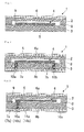
- Fig. 1 is a schematic diagram in vertical section showing an electronic device 1 according to a first embodiment of the invention.
- the electronic device 1 includes a lid substrate 2 made of soda-lime glass, a base substrate 3 made of soda-lime glass, bonded to the lid substrate 2, and forming a cavity 4 hermetically sealed from the outside air between the base substrate 3 and the lid substrate 2, an electronic element 5 housed in the cavity 4 and surface-mounted on the base substrate 3, and a mold member 6 placed on an outer face of the lid substrate 2 on the side opposite to the cavity 4.
- the lid substrate 2 and the base substrate 3 are bonded together with a metal material 8 interposed between them.
- the cavity 4 is formed of a recess portion 9 formed in the lid substrate 2.
- the lid substrate 2 is easily warped such that the side of the recess portion 9 protrudes.
- the mold member 6 is placed on the surface of the lid substrate 2 on the side opposite to the recess portion 9.
- the soda-lime glass has a coefficient of linear expansion of 9 to 11 (ppm/°C), and the mold member 6 is set to have a coefficient of linear expansion smaller than that of the soda-lime glass.
- a mold material is applied to the surface of the lid substrate 2 and thermally cured at a temperature of 100°C or higher to form the mold member 6.
- the lid substrate 2 When the mold member 6 is cooled to room temperature, the lid substrate 2 has the coefficient of linear expansion larger than the coefficient of linear expansion of the mold member 6 and thus the outer face of the lid substrate 2 is subjected to a compressive stress. Since this corrects the warping of the lid substrate 2 in which the side of the recess portion 9 protrudes, the lid substrate 2 is flattened.
- the coefficient of linear expansion of the mold member 6 can be adjusted by the type and the amount of the filler contained in the mold member 6. When epoxy resin filled with silica is used as the mold material, the filling amount of the silica can be increased to reduce the coefficient of linear expansion of the mold member 6.
- the warping of the lid substrate 2 is reduced to facilitate the alignment of the lid substrate 2 and the base substrate 3. This allows the use of a large substrate from which a number of devices can be obtained, so that the cost of the electronic device can be reduced.
- the reduced warping of the electronic device 1 relieves variations in stress applied to the electronic element resulting from a change in ambient temperature, which stabilizes the characteristics of the electronic element.
- Fig. 2 is a schematic diagram in vertical section showing an electronic device 1 according to a second embodiment of the invention.
- the electronic device 1 includes a lid substrate 2 made of soda-lime glass, a base substrate 3 made of soda-lime glass, bonded to the lid substrate 2, and forming a cavity 4 hermetically sealed from the outside air between the base substrate 3 and the lid substrate 2, an electronic element 5 housed in the cavity 4 and surface-mounted on the base substrate 3, and mold members 6a and 6b placed on outer faces of the lid substrate 2 and the base substrate 3, respectively.
- the electronic device 1 further includes through electrodes 7a and 7b passing through the base substrate 3, and electrode terminals 10a and 10b formed on an outer face of the mold member 6b and passing through the mold member 6b to electrically connect to the through electrodes 7a and 7b, respectively.
- the electronic element 5 is electrically connected to the through electrodes 7a and 7b through an electrode, not shown, and is mounted on the base substrate 3. Thus, the electronic element 5 can be supplied with power from the outside and can perform transmission to the outside through the electrode terminals 10a and 10b.
- the coefficient of linear expansion of the mold member 6b may be adjusted on the basis of the warping of the base substrate 3 or warping of the lid substrate 2 and the base substrate 3 bonded together. For example when the base substrate 3 alone or the lid substrate 2 and the base substrate 3 bonded together are easily warped such that the side of the electronic element 5 protrudes, the coefficient of linear expansion of the mold member 6b may be set to be smaller than the coefficient of linear expansion of the soda-lime glass.
- the mold member 6b serves as a shock-absorbing member when the electronic device 1 is mounted on a substrate or the like.
- the through electrodes 7a and 7b are directly bonded to a mounting electrode on the substrate or the like in mounting the electronic device 1 on the substrate or the like.
- a large stress is applied to the through electrodes 7a and 7b in mounting the electronic device 1 or due to other environmental changes to cause a defect such as chipping or cracking in the base substrate 3 near the through electrodes 7a and 7b, for example the glass substrate.
- the mold member 6b and the electrode terminals 10a and 10b are present between the electrode on the mounting substrate and the through electrodes 7a and 7b in the present embodiment, so that the stress applied to the base substrate 3 near the through electrodes 7a and 7b can be relieved to prevent occurrence of cracking or chipping in the base substrate 3.
- the mold members 6a and 6b are placed on the outer faces of the lid substrate 2 and the base substrate 3 in this manner, the warping of each of the lid substrate 2 and the base substrate 3 is reduced to relieve the stress applied to the electronic element 5 to stabilize the characteristics.
- variations in stress applied to the electronic element resulting from a change in ambient temperature can be reduced to stabilize the characteristics of the electronic element.
- the mold members 6a and 6b can serve as the stress relieving layers to prevent the occurrence of cracking or chipping in the base substrate 3 due to environmental changes.
- the mold members 6a and 6b may, but need not, have different coefficients of linear expansion.
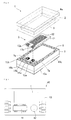
- Fig. 3 and Fig. 4 are a schematic diagram in vertical section and an exploded perspective view showing an electronic device 1 according to a third embodiment of the invention, respectively.
- the third embodiment differs from the second embodiment in that an electronic element 5 is mounted in the form of a cantilever on a base substrate 3, and the other configurations are substantially similar to those of the second embodiment.
- description is mainly made of the different points.
- the same portions or the portions having the same functions are designated with the same reference numerals.
- a lid substrate 2 and the base substrate 3 are anodic-bonded on the outer peripheral portions of the substrates by using a metal material 8 as a bonding material.
- the electronic element 5 is formed of a piezoelectric vibrating strip 11 made of monocrystalline crystal, an exciting electrode 12 formed on each face of the piezoelectric vibrating strip 11, and connecting electrodes 13a and 13b electrically connected to the exciting electrode 12.
- the electronic element 5 is mounted such that one end portion thereof is cantilevered on two mounting portions 14a and 14b.
- the two connecting electrodes 13a and 13b are connected to electrode terminals 10a and 10b (or 10c) through the mounting portions 14a and 14b, routing electrodes 15a and 15b, and through electrodes 7a and 7b, respectively, such that the electrodes 13a and 13b are electrically isolated from each other.
- the coefficient of linear expansion of a mold member 6b can be set to be smaller than the coefficient of linear expansion of the lid substrate 2 or the base substrate 3, for example the coefficient of linear expansion of the soda-lime glass.
- the coefficient of linear expansion of the mold member 6b can be set to be larger than the coefficient of linear expansion of the soda-lime glass.
- an AT-cut crystal vibrating strip is used as the piezoelectric vibrating strip 11.
- Each of the lid substrate 2 and the base substrate 3 has an outer diameter of approximately 2 mm x approximately 1 mm.
- Each of the lid substrate 2 and the base substrate 3 has a thickness of approximately 0.2 mm.
- Each of the mold members 6a and 6b has a thickness of approximately 50 ⁇ m.
- a recess portion 9 formed in the lid substrate 2 has a depth of approximately 0.1 mm. Vacuum is maintained in a cavity 4, and the vibrations of the piezoelectric vibrating strip 11 do not undergo air resistance.
- the mold members 6a and 6b are placed on the outer faces of the lid substrate 2 and the base substrate 3 in this manner, the warping of each of the lid substrate 2 and the base substrate 3 is reduced to facilitate the alignment in bonding the lid substrate 2 to the base substrate 3, and the stress applied to the piezoelectric vibrating strip 11 is reduced to relieve variations in the vibration rate of the piezoelectric vibrating strip 11. In addition, the frequency characteristics are stabilized when the ambient temperature is changed. Furthermore, the mold member 6b can serve as a buffer member to prevent the occurrence of cracking or chipping in the base substrate 3 in mounting the electronic device 1 or due to other environmental changes. Since the mold members 6a and 6b serve as the outer peripheral face of the electronic device 1, an identification number or the like can be marked on the mold member 6a or 6b to ensure the specification of each product.
- Fig. 5 is a schematic diagram of a top face showing an oscillator 40 according to a fourth embodiment of the invention.
- the oscillator 40 has the electronic device 1 incorporated therein which employs the piezoelectric vibrating strip 11 made of monocrystalline crystal shown in the third embodiment.
- the oscillator 40 includes a substrate 43, the electronic device 1 placed on the substrate, an integrated circuit 41, and an electronic part 42.
- the electronic device 1 produces a signal at a certain frequency based on a driving signal supplied to the electrode terminals 10a and 10b.
- the integrated circuit 41 and the electronic part 42 process the signal at the certain frequency supplied from the electronic device 1 to produce a reference signal such as a clock signal. Since the electronic device 1 according to the invention can be formed with high reliability and small size, the overall oscillator 40 can be made compact.
- a method of manufacturing the electronic device includes a recess portion forming step of forming the recess portion in the lid substrate, a mounting step of mounting the electronic element on the base substrate, a mold member placing step of placing the mold member on the outer face of one or both of the lid substrate and the base substrate, and a bonding step of bonding the lid substrate to the base substrate with the electronic element housed in the recess portion.
- the mold member placed on the outer face of one or both of the lid substrate and the base substrate can reduce warping of the lid substrate or the base substrate to facilitate the alignment of the lid substrate and the base substrate.
- the mounting of the electronic part can be facilitated at the mounting step to reduce the occurrence of defects.
- the reduced warping of the substrate allows the use of a large substrate from which a number of devices can be obtained, thereby cutting the cost of the electronic device.
- variations in characteristics of the electronic element can be reduced when environmental changes occur, so that the quality of the electronic device can be improved.
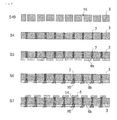
- Fig. 6 to Fig. 9 are diagrams for explaining the method of manufacturing the electronic device according to a fifth embodiment of the invention.
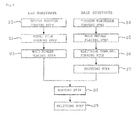
- Fig. 6 is a process diagram showing the method of manufacturing the electronic device.
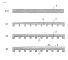
- Fig. 7 , Fig. 8 , and Fig. 9 are explanatory diagrams for the respective steps.
- soda-lime glass is used as the lid substrate 2 and the base substrate 3, and the electronic element 5 is formed of a crystal oscillator.
- a method of manufacturing the lid substrate 2 is described with reference to Fig. 6 and Fig. 7 .
- the lid substrate 2 in plate shape is prepared at a lid substrate preparing step S10.
- the lid substrate 2 is placed in a mold with a molding method and is pressed while heating, thereby forming a plurality of recess portions 9 simultaneously.
- a number of recess portions 9 having a depth of approximately 0.1 mm are simultaneously formed in a soda-lime glass plate having an outer diameter of 4 inches and a thickness of approximately 0.2 mm.
- a number of recess portions 9 may be formed simultaneously in this recess forming step S1 with a sandblast method or an etching method by placing a mask on the surface of the lid substrate 2, instead of the formation with the molding.
- a metal film 17 made of aluminum containing amorphous silicon is deposited on the surface of the lid substrate 2 on the side of the recess portion 9 with a sputtering method.
- the metal film 17 is used as a bonding material between the lid substrate 2 and the base substrate 3 at a later step.
- the metal film 17 may be deposited with an evaporation method or a plating method. Another metal material can be used as required.
- the mold member 6a is placed on the outer face of the lid substrate 2 on the side opposite to the recess portion 9.
- An epoxy resin material filled with silica is used as the mold material, is applied to the outer face of the lid substrate 2, and is cured through heating to a temperature of approximately 150C° to form the mold member 6a.
- the mold member 6a is formed with a thickness of 20 ⁇ m to 100 ⁇ m, preferably with a thickness of 50 ⁇ m.
- a method of manufacturing the base substrate 3 is described with reference to Fig. 6 and Fig. 8 .
- the base substrate 3 in plate shape is prepared, and a plurality of through holes 16 are formed in the base substrate 3 at a through hole forming step S40.
- the plurality of through holes 16 can be formed simultaneously with the molding method similarly to the formation of the recess portions 9. Instead of the molding method, the plurality of through holes 16 can be formed simultaneously with the sandblasting method or the etching method by placing a mask on the surface.
- the through holes 16 having a diameter of 50 ⁇ m to 0.3 mm are formed with a pitch of approximately 0.5 mm to 2 mm in a vertical direction and a horizontal direction in a soda-lime glass plate having an outer diameter of 4 inches and a thickness of approximately 0.2 mm.
- the through hole 16 is filled with a metal material to provide the through electrode 7 at a through electrode forming step S4.
- a metal rod can be inserted into the through hole 16, and the glass and the metal rod can be hermetically bonded together through heat welding or an adhesive.
- the surface of the base substrate 3 is planarized by grinding or polishing.
- the mold member 6b is placed such that an end face of the through electrode 7 is exposed on a lower face of the base substrate 3 at the mold member placing step S5.
- An epoxy resin material filled with silica is used as the mold material, is applied to the outer face of the base substrate 3, and is cured through heating to a temperature of approximately 150°C to form the mold member 6b.
- the mold member 6b is formed to have a thickness of 20 ⁇ m to 100 ⁇ m, preferably a thickness of 50 ⁇ m.
- the coefficient of linear expansion of the mold member 6b is set by adjusting the type or the amount of the filler in consideration of the state of warping of the base substrate 3 or the state of warping of the base substrate 3 after the bonding to the lid substrate 2.
- the coefficient of linear expansion of the mold member 6b is set to be smaller than the coefficient of linear expansion of the soda-lime glass.
- the coefficient of linear expansion of the mold member 6b is set to be larger than the coefficient of linear expansion of the soda-lime glass.
- the electrode terminal 10 is formed on the face of the mold member 6b and the exposed face of the through electrode 7 on the side of the mole member 6b at an electrode terminal forming step S6.
- the electrode terminal 10 can be formed by depositing a metal film on the outer face of the mold member 6b with the evaporation method, the sputtering method, or the plating method and patterning the film with the photolithography and etching method.
- the electrode terminal 10 can be provided by printing and thermally treating a pattern formed of a conductive material.
- the electronic element 5 is mounted in the form of a cantilever over an upper face of the base substrate 3 with the mounting portion 14 interposed. This causes the connecting electrode, not shown, formed on the face of the electronic element 5 to be electrically connected to the electrode terminal 10 through the mounting portion 14 and the through electrode 7.
- the electronic element 5 is a crystal vibrator with one end fixed to the mounting portion 14 and the other end separated from the base substrate 3 for vibration.
- the bonding step S8 and a splitting step S9 for the lid substrate 2 and the base substrate 3 are described with reference to Fig. 6 and Fig. 9 .
- the lid substrate 2 and the base substrate 3 are placed one on another with the metal film 17 interposed between them such that the electronic element 5 mounted on the base substrate 3 is housed in the recess portion 9 of the lid substrate 2.
- the bonding step S8 is performed under vacuum. Since the mold members 6a and 6b are placed on the outer faces of the lid substrate 2 and the base substrate 3, respectively, each of the substrates is warped only slightly to allow easy alignment thereof.
- the lid substrate 2 and the base substrate 3 are heated, and a high voltage is applied between the lid substrate 2 and the base substrate 3 to anodic-bond the abutting portions of the substrates.
- a high voltage is applied between the lid substrate 2 and the base substrate 3 to anodic-bond the abutting portions of the substrates.
- heating is performed to a temperature of 200°C to 250°C, and a voltage of 500V is applied to the lid substrate 2 and the base substrate 3 to perform the anodic bonding.
- the substrates are split into individual electronic devices 1 by a dicer at the splitting step S9.
- the warping amount of each of the substrates is reduced to facilitate the alignment in this manner, a larger substrate can be used to form a number of electronic devices 1 simultaneously to cut the cost.
- variations in stress applied to the electronic element due to a change in ambient temperature can be reduced to stabilize the characteristics of the electronic element to improve the quality of the electronic device.
- the metal film 17 is formed on the lid substrate 2 in the present embodiment, the metal film 17 may be formed on the base substrate 3. While the metal film 17 is formed on the side face and the bottom face of the recess portion 9 of the lid substrate 2 in the present embodiment, the metal film 17 on the bottom face and the side face of the recess portion 9 may be removed since it is only required that the metal film 17 should serve as the bonding material.
- the anodic bonding is not essential in the invention, and for example, the lid substrate 2 and the base substrate 3 may be bonded together by using an adhesive.
- the mold members 6a and 6b are formed on the outer faces of the substrates before the bonding of the lid substrate 2 and the base substrate 3 in the embodiments described above, the invention is not limited thereto, and the mold members 6a and 6b may be placed on the outer face of the lid substrate 2 or the base substrate 3 after the bonding of the lid substrate 2 and the base substrate 3. This is limited to the case where the lid substrate 2 and the base substrate 3 can be aligned.
- the mold material is applied to the substrate face to form the mold member 6 in the embodiments described above, the invention is not limited thereto.
- the mold member 6 may be formed with transfer molding by placing the lid substrate 2 and the base substrate 3 in a mold and pouring a mold material into the mold.
Landscapes
- Physics & Mathematics (AREA)
- Acoustics & Sound (AREA)
- Piezo-Electric Or Mechanical Vibrators, Or Delay Or Filter Circuits (AREA)
- Oscillators With Electromechanical Resonators (AREA)
Abstract
Description
- The present invention relates to an electronic device including an electronic element mounted in a cavity formed between two substrates, an oscillator, and a method of manufacturing the electronic device.
- Portable information terminals such as cellular phones widely available in recent years often employ electronic devices with small packages of a surface mount type. For example, a vibrator, a MEMS, a gyrosensor, an acceleration sensor or the like has a structure in which an electronic element is housed in a package of a hollow cavity structure. A known example of the package of the hollow cavity type is provided by anodic-bonding a base substrate to a lid substrate with a metal film interposed between them. A method of the anodic bonding is described, for example in
JP-A-9-2845 -
Fig. 10 shows a method of simultaneously forming a number ofelectronic devices 50 of this type. First, abase substrate 51 and alid substrate 52 are prepared. Next, a plurality of through holes are formed in thebase substrate 51, and a conductive material is embedded in each of the through holes to provide a throughelectrode 56. Anelectrode terminal 58 is formed on a back face of thebase substrate 51 for electrical connection to the throughelectrode 56. A number ofelectronic elements 55 are mounted on a front face of thebase substrate 51. In mounting of theelectronic element 55, theelectronic element 55 is electrically connected to the throughelectrode 56. - A number of
recess portions 59 are formed in thelid substrate 52. Then, thebase substrate 51 is overlaid on thelid substrate 52 and they are bonded together. The bonding is performed with an adhesive or anodic bonding. Therecess portion 59 in thelid substrate 52 provides acavity 54, and theelectronic element 55 is housed in thecavity 54. Then, the substrates are split into individual electronic devices. - As shown in
Fig. 10 , however, thebase substrate 51 and thelid substrate 52 are deformed when thethrough electrodes 56 and therecess portions 59 are formed. This reduces the accuracy of the alignment of thelid substrate 52 and thebase substrate 51. Warping also occurs as shown inFig. 10 after the bonding of thebase substrate 51 to thelid substrate 52. The substrates are significantly warped, especially when the outer diameters of thebase substrate 51 and thelid substrate 52 are increased to obtain a larger number of devices, which makes it difficult to align thebase substrate 51 with thelid substrate 52. In addition, a change in ambient temperature changes the stress applied to the mountedelectronic element 55, and the stress change disadvantageously varies the characteristics of theelectronic element 55. - The invention has been made in view of the problems described above, and it is an object thereof to provide an electronic device with reduced deformation of a substrate, and a method of manufacturing the same.
- An electronic device according to a first aspect of the invention includes a lid substrate, a base substrate bonded to the lid substrate and forming a cavity hermetically sealed from the outside air between the base substrate and the lid substrate, an electronic element housed in the cavity, and a mold member placed on an outer face of the lid substrate or the base substrate.
- Preferably, the lid substrate has a recess portion and the recess portion forms the cavity.
- Preferably, the base substrate has a through electrode passing from an inner face on the side of the cavity to an outer face on the side opposite to the cavity, and the electronic element is electrically connected to the through electrode.
- Preferably, the lid substrate and the base substrate are bonded together with a bonding material including a metal material interposed between them.
- Preferably, the electronic element is a crystal vibrator mounted in the form of a cantilever on the inner face of the base substrate.
- Preferably, the mold member is formed of an epoxy resin.
- An oscillator according to a second aspect of the invention includes the electronic device described in any of the above, and a driving circuit supplying a driving signal to the electronic device.
- A method of manufacturing an electronic device according to a third aspect the invention includes a recess portion forming step of forming a recess portion in a lid substrate, a mounting step of mounting an electronic element on a base substrate, a mold member placing step of placing a mold member on an outer face of the lid substrate or the base substrate, and a bonding step of bonding the lid substrate to the base substrate with the electronic element housed in the recess portion.
- Preferably, the mold member placing step is performed before the bonding step.
- Preferably, the mold member placing step is performed after the bonding step.
- Preferably, a through electrode forming step of forming a through electrode in the base substrate is further included, and the mold member placing step is a step of placing the mold member such that the through electrode is exposed on an outer face of the base substrate on the side opposite to the side where the electronic element is mounted.
- Preferably, the recess portion forming step is a step of mounting a plurality of recess portions in the lid substrate, and the mounting step is a step of mounting a plurality of the electronic elements on the base substrate. A splitting step of cutting and splitting a stack formed of the lid substrate and the base substrate bonded together is included.
- The electronic device according to the invention includes the lid substrate, the base substrate bonded to the lid substrate and forming the cavity between the base substrate and the lid substrate, the electronic element housed in the cavity, and the mold member placed on the outer face of the lid substrate or the base substrate. The mold member placed on the outer face of the lid substrate or the base substrate can reduce warping of the substrate to facilitate alignment of the lid substrate and the base substrate, thereby reducing the rate of occurrence of defects. In addition, variations in stress applied to the electronic element from the lid substrate or the base substrate can be reduced to stabilize the characteristics of the electronic element.
- Embodiments of the present invention will now be described by way of further example only and with reference to the accompanying drawings, in which:
-
Fig. 1 is a schematic diagram in vertical section showing an electronic device according to a first embodiment of the invention. -
Fig. 2 is a schematic diagram in vertical section showing an electronic device according to a second embodiment of the invention. -
Fig. 3 is a schematic diagram in vertical section showing an electronic device according to a third embodiment of the invention. -
Fig. 4 is an exploded perspective view showing the electronic device according to the third embodiment of the invention. -
Fig. 5 is a schematic diagram of a top face showing an oscillator according to a fourth embodiment of the invention. -
Fig. 6 is a process diagram showing a method of manufacturing an electronic device according to a fifth embodiment of the invention. -
Fig. 7 is a diagram for explaining the method of manufacturing the electronic device according to the fifth embodiment of the invention. -
Fig. 8 is a diagram for explaining the method of manufacturing the electronic device according to the fifth embodiment of the invention. -
Fig. 9 is a diagram for explaining the method of manufacturing the electronic device according to the fifth embodiment of the invention. -
Fig. 10 shows a method of simultaneously forming a number of electronic devices conventionally known. - An electronic device according to the invention includes a lid substrate, a base substrate bonded to the lid substrate and forming a cavity between the base substrate and the lid substrate, an electronic element housed in the cavity, and a mold member placed on an outer face of the lid substrate or the base substrate.
- The configuration of the invention can reduce warping of the lid substrate or the base substrate to facilitate the alignment of the lid substrate and the base substrate, thereby reducing the rate of occurrence of defects. The reduced warping of the substrate allows the use of a large glass substrate from which a number of devices can be obtained, so that the cost of the electronic device can be cut. In addition, the reduced warping of the substrate relieves variations in stress applied to the electronic element resulting from a change in ambient temperature, which stabilizes the characteristics of the electronic element.
- The lid substrate and the base substrate can be provided by using glass, ceramics, synthetic resin, or other materials. When a glass material is used, working thereof is easily performed and impregnation with water or other impurities can be prevented, and therefore, a package can be formed at low cost and with high reliability. The cavity may be formed of a recess portion formed in the lid substrate or a recess portion formed in the base substrate. The electronic element may be mounted on an inner face of the lid substrate or may be mounted on an inner face of the base substrate.
- The mold member may be formed on the outer face of the lid substrate, may be formed on the outer face of the base substrate, or may be formed on each of the outer faces of both of the lid substrate and the base substrate. The mold member can be provided by using a resin material, for example an epoxy resin and a filler added thereto. The filler can be provided by using silica, alumina, alumina powder or the like. The coefficient of linear expansion of the mold member can be adjusted on the basis of the type and the amount of the filler. Since the mold member serves as the outer peripheral face of the electronic device, an identification number or the like can be marked on the mold member to ensure the specification of each product.
- The lid substrate and the base substrate are bonded together by using an adhesive or can be anodic-bonded with a metal material interposed between them. The anodic bonding can provide a highly hermetic cavity. An electrical connection from the electronic element enclosed in the cavity to the outside can be made through an electrode formed on a bonding face of the lid substrate and/or the base substrate or can be made through a through electrode passing through the base substrate and/or the lid substrate.
-
Fig. 1 is a schematic diagram in vertical section showing anelectronic device 1 according to a first embodiment of the invention. Theelectronic device 1 includes alid substrate 2 made of soda-lime glass, abase substrate 3 made of soda-lime glass, bonded to thelid substrate 2, and forming acavity 4 hermetically sealed from the outside air between thebase substrate 3 and thelid substrate 2, anelectronic element 5 housed in thecavity 4 and surface-mounted on thebase substrate 3, and amold member 6 placed on an outer face of thelid substrate 2 on the side opposite to thecavity 4. Thelid substrate 2 and thebase substrate 3 are bonded together with ametal material 8 interposed between them. Thecavity 4 is formed of arecess portion 9 formed in thelid substrate 2. - After the
recess portion 9 is formed, thelid substrate 2 is easily warped such that the side of therecess portion 9 protrudes. To address this, themold member 6 is placed on the surface of thelid substrate 2 on the side opposite to therecess portion 9. In this case, the soda-lime glass has a coefficient of linear expansion of 9 to 11 (ppm/°C), and themold member 6 is set to have a coefficient of linear expansion smaller than that of the soda-lime glass. A mold material is applied to the surface of thelid substrate 2 and thermally cured at a temperature of 100°C or higher to form themold member 6. When themold member 6 is cooled to room temperature, thelid substrate 2 has the coefficient of linear expansion larger than the coefficient of linear expansion of themold member 6 and thus the outer face of thelid substrate 2 is subjected to a compressive stress. Since this corrects the warping of thelid substrate 2 in which the side of therecess portion 9 protrudes, thelid substrate 2 is flattened. The coefficient of linear expansion of themold member 6 can be adjusted by the type and the amount of the filler contained in themold member 6. When epoxy resin filled with silica is used as the mold material, the filling amount of the silica can be increased to reduce the coefficient of linear expansion of themold member 6. - Since the
mold member 6 is placed on the outer face of thelid substrate 2 in this manner, the warping of thelid substrate 2 is reduced to facilitate the alignment of thelid substrate 2 and thebase substrate 3. This allows the use of a large substrate from which a number of devices can be obtained, so that the cost of the electronic device can be reduced. In addition, the reduced warping of theelectronic device 1 relieves variations in stress applied to the electronic element resulting from a change in ambient temperature, which stabilizes the characteristics of the electronic element. -
Fig. 2 is a schematic diagram in vertical section showing anelectronic device 1 according to a second embodiment of the invention. Theelectronic device 1 includes alid substrate 2 made of soda-lime glass, abase substrate 3 made of soda-lime glass, bonded to thelid substrate 2, and forming acavity 4 hermetically sealed from the outside air between thebase substrate 3 and thelid substrate 2, anelectronic element 5 housed in thecavity 4 and surface-mounted on thebase substrate 3, andmold members lid substrate 2 and thebase substrate 3, respectively. - The
electronic device 1 further includes throughelectrodes base substrate 3, andelectrode terminals mold member 6b and passing through themold member 6b to electrically connect to the throughelectrodes electronic element 5 is electrically connected to the throughelectrodes base substrate 3. Thus, theelectronic element 5 can be supplied with power from the outside and can perform transmission to the outside through theelectrode terminals - Since the
mold member 6b is also placed on the outer face of thebase substrate 3 in the present embodiment, warping of thebase substrate 3 can be reduced. The coefficient of linear expansion of themold member 6b may be adjusted on the basis of the warping of thebase substrate 3 or warping of thelid substrate 2 and thebase substrate 3 bonded together. For example when thebase substrate 3 alone or thelid substrate 2 and thebase substrate 3 bonded together are easily warped such that the side of theelectronic element 5 protrudes, the coefficient of linear expansion of themold member 6b may be set to be smaller than the coefficient of linear expansion of the soda-lime glass. - In addition, the
mold member 6b serves as a shock-absorbing member when theelectronic device 1 is mounted on a substrate or the like. Specifically, when themold member 6b is not used, the throughelectrodes electronic device 1 on the substrate or the like. A large stress is applied to the throughelectrodes electronic device 1 or due to other environmental changes to cause a defect such as chipping or cracking in thebase substrate 3 near the throughelectrodes mold member 6b and theelectrode terminals electrodes base substrate 3 near the throughelectrodes base substrate 3. - Since the
mold members lid substrate 2 and thebase substrate 3 in this manner, the warping of each of thelid substrate 2 and thebase substrate 3 is reduced to relieve the stress applied to theelectronic element 5 to stabilize the characteristics. In addition, variations in stress applied to the electronic element resulting from a change in ambient temperature can be reduced to stabilize the characteristics of the electronic element. Furthermore, themold members base substrate 3 due to environmental changes. Thus, the electronic device with stable characteristics, high reliability, and high quality can be provided. Themold members -
Fig. 3 andFig. 4 are a schematic diagram in vertical section and an exploded perspective view showing anelectronic device 1 according to a third embodiment of the invention, respectively. The third embodiment differs from the second embodiment in that anelectronic element 5 is mounted in the form of a cantilever on abase substrate 3, and the other configurations are substantially similar to those of the second embodiment. In the following, description is mainly made of the different points. The same portions or the portions having the same functions are designated with the same reference numerals. - A
lid substrate 2 and thebase substrate 3 are anodic-bonded on the outer peripheral portions of the substrates by using ametal material 8 as a bonding material. Theelectronic element 5 is formed of a piezoelectric vibratingstrip 11 made of monocrystalline crystal, anexciting electrode 12 formed on each face of the piezoelectric vibratingstrip 11, and connectingelectrodes exciting electrode 12. Theelectronic element 5 is mounted such that one end portion thereof is cantilevered on two mountingportions electrodes electrode terminals portions routing electrodes electrodes electrodes lid substrate 2 and thebase substrate 3 bonded together are easily warped with the side of thelid substrate 2 protruded, the coefficient of linear expansion of amold member 6b can be set to be smaller than the coefficient of linear expansion of thelid substrate 2 or thebase substrate 3, for example the coefficient of linear expansion of the soda-lime glass. Alternatively, when thelid substrate 2 and thebase substrate 3 bonded together are easily warped with the side of thebase substrate 3 protruded, the coefficient of linear expansion of themold member 6b can be set to be larger than the coefficient of linear expansion of the soda-lime glass. - In the present embodiment, an AT-cut crystal vibrating strip is used as the piezoelectric vibrating
strip 11. Each of thelid substrate 2 and thebase substrate 3 has an outer diameter of approximately 2 mm x approximately 1 mm. Each of thelid substrate 2 and thebase substrate 3 has a thickness of approximately 0.2 mm. Each of themold members recess portion 9 formed in thelid substrate 2 has a depth of approximately 0.1 mm. Vacuum is maintained in acavity 4, and the vibrations of the piezoelectric vibratingstrip 11 do not undergo air resistance. - Since the
mold members lid substrate 2 and thebase substrate 3 in this manner, the warping of each of thelid substrate 2 and thebase substrate 3 is reduced to facilitate the alignment in bonding thelid substrate 2 to thebase substrate 3, and the stress applied to the piezoelectric vibratingstrip 11 is reduced to relieve variations in the vibration rate of the piezoelectric vibratingstrip 11. In addition, the frequency characteristics are stabilized when the ambient temperature is changed. Furthermore, themold member 6b can serve as a buffer member to prevent the occurrence of cracking or chipping in thebase substrate 3 in mounting theelectronic device 1 or due to other environmental changes. Since themold members electronic device 1, an identification number or the like can be marked on themold member -
Fig. 5 is a schematic diagram of a top face showing anoscillator 40 according to a fourth embodiment of the invention. Theoscillator 40 has theelectronic device 1 incorporated therein which employs the piezoelectric vibratingstrip 11 made of monocrystalline crystal shown in the third embodiment. As shown inFig. 5 , theoscillator 40 includes asubstrate 43, theelectronic device 1 placed on the substrate, anintegrated circuit 41, and anelectronic part 42. Theelectronic device 1 produces a signal at a certain frequency based on a driving signal supplied to theelectrode terminals integrated circuit 41 and theelectronic part 42 process the signal at the certain frequency supplied from theelectronic device 1 to produce a reference signal such as a clock signal. Since theelectronic device 1 according to the invention can be formed with high reliability and small size, theoverall oscillator 40 can be made compact. - A method of manufacturing the electronic device according to the invention includes a recess portion forming step of forming the recess portion in the lid substrate, a mounting step of mounting the electronic element on the base substrate, a mold member placing step of placing the mold member on the outer face of one or both of the lid substrate and the base substrate, and a bonding step of bonding the lid substrate to the base substrate with the electronic element housed in the recess portion.
- The mold member placed on the outer face of one or both of the lid substrate and the base substrate can reduce warping of the lid substrate or the base substrate to facilitate the alignment of the lid substrate and the base substrate. In addition, when the mold member is placed on the base substrate, the mounting of the electronic part can be facilitated at the mounting step to reduce the occurrence of defects. The reduced warping of the substrate allows the use of a large substrate from which a number of devices can be obtained, thereby cutting the cost of the electronic device. At the same time, variations in characteristics of the electronic element can be reduced when environmental changes occur, so that the quality of the electronic device can be improved.
-
Fig. 6 to Fig. 9 are diagrams for explaining the method of manufacturing the electronic device according to a fifth embodiment of the invention.Fig. 6 is a process diagram showing the method of manufacturing the electronic device.Fig. 7 ,Fig. 8 , andFig. 9 are explanatory diagrams for the respective steps. In the present embodiment, soda-lime glass is used as thelid substrate 2 and thebase substrate 3, and theelectronic element 5 is formed of a crystal oscillator. - A method of manufacturing the
lid substrate 2 is described with reference toFig. 6 andFig. 7 . First, thelid substrate 2 in plate shape is prepared at a lid substrate preparing step S10. Next, thelid substrate 2 is placed in a mold with a molding method and is pressed while heating, thereby forming a plurality ofrecess portions 9 simultaneously. For example, a number ofrecess portions 9 having a depth of approximately 0.1 mm are simultaneously formed in a soda-lime glass plate having an outer diameter of 4 inches and a thickness of approximately 0.2 mm. A number ofrecess portions 9 may be formed simultaneously in this recess forming step S1 with a sandblast method or an etching method by placing a mask on the surface of thelid substrate 2, instead of the formation with the molding. - Next, at a metal film forming step S2, a
metal film 17 made of aluminum containing amorphous silicon is deposited on the surface of thelid substrate 2 on the side of therecess portion 9 with a sputtering method. Themetal film 17 is used as a bonding material between thelid substrate 2 and thebase substrate 3 at a later step. Themetal film 17 may be deposited with an evaporation method or a plating method. Another metal material can be used as required. - Next, at the mold member placing step S3, the
mold member 6a is placed on the outer face of thelid substrate 2 on the side opposite to therecess portion 9. An epoxy resin material filled with silica is used as the mold material, is applied to the outer face of thelid substrate 2, and is cured through heating to a temperature of approximately 150C° to form themold member 6a. Themold member 6a is formed with a thickness of 20 µm to 100 µm, preferably with a thickness of 50 µm. - A method of manufacturing the
base substrate 3 is described with reference toFig. 6 andFig. 8 . First, thebase substrate 3 in plate shape is prepared, and a plurality of throughholes 16 are formed in thebase substrate 3 at a through hole forming step S40. The plurality of throughholes 16 can be formed simultaneously with the molding method similarly to the formation of therecess portions 9. Instead of the molding method, the plurality of throughholes 16 can be formed simultaneously with the sandblasting method or the etching method by placing a mask on the surface. For example, the throughholes 16 having a diameter of 50 µm to 0.3 mm are formed with a pitch of approximately 0.5 mm to 2 mm in a vertical direction and a horizontal direction in a soda-lime glass plate having an outer diameter of 4 inches and a thickness of approximately 0.2 mm. - Next, the through
hole 16 is filled with a metal material to provide the throughelectrode 7 at a through electrode forming step S4. For example, a metal rod can be inserted into the throughhole 16, and the glass and the metal rod can be hermetically bonded together through heat welding or an adhesive. Then, the surface of thebase substrate 3 is planarized by grinding or polishing. - Next, the
mold member 6b is placed such that an end face of the throughelectrode 7 is exposed on a lower face of thebase substrate 3 at the mold member placing step S5. An epoxy resin material filled with silica is used as the mold material, is applied to the outer face of thebase substrate 3, and is cured through heating to a temperature of approximately 150°C to form themold member 6b. Themold member 6b is formed to have a thickness of 20 µm to 100 µm, preferably a thickness of 50 µm. The coefficient of linear expansion of themold member 6b is set by adjusting the type or the amount of the filler in consideration of the state of warping of thebase substrate 3 or the state of warping of thebase substrate 3 after the bonding to thelid substrate 2. More specifically, when thebase substrate 3 is warped with the mount side of theelectronic element 5 protruded or when thebase substrate 3 bonded to thelid substrate 2 is warped with the side of thelid substrate 2 protruded, the coefficient of linear expansion of themold member 6b is set to be smaller than the coefficient of linear expansion of the soda-lime glass. Conversely, when thebase substrate 3 is warped with the side of themold member 6b protruded or when thelid substrate 2 and thebase substrate 3 bonded together are warped with the side of thebase substrate 3 protruded, the coefficient of linear expansion of themold member 6b is set to be larger than the coefficient of linear expansion of the soda-lime glass. - Next, the
electrode terminal 10 is formed on the face of themold member 6b and the exposed face of the throughelectrode 7 on the side of themole member 6b at an electrode terminal forming step S6. Theelectrode terminal 10 can be formed by depositing a metal film on the outer face of themold member 6b with the evaporation method, the sputtering method, or the plating method and patterning the film with the photolithography and etching method. Alternatively, theelectrode terminal 10 can be provided by printing and thermally treating a pattern formed of a conductive material. - Next, at the mounting
step 7, theelectronic element 5 is mounted in the form of a cantilever over an upper face of thebase substrate 3 with the mountingportion 14 interposed. This causes the connecting electrode, not shown, formed on the face of theelectronic element 5 to be electrically connected to theelectrode terminal 10 through the mountingportion 14 and the throughelectrode 7. In the present embodiment, theelectronic element 5 is a crystal vibrator with one end fixed to the mountingportion 14 and the other end separated from thebase substrate 3 for vibration. - The bonding step S8 and a splitting step S9 for the
lid substrate 2 and thebase substrate 3 are described with reference toFig. 6 andFig. 9 . At the bonding step S8, thelid substrate 2 and thebase substrate 3 are placed one on another with themetal film 17 interposed between them such that theelectronic element 5 mounted on thebase substrate 3 is housed in therecess portion 9 of thelid substrate 2. The bonding step S8 is performed under vacuum. Since themold members lid substrate 2 and thebase substrate 3, respectively, each of the substrates is warped only slightly to allow easy alignment thereof. Next, thelid substrate 2 and thebase substrate 3 are heated, and a high voltage is applied between thelid substrate 2 and thebase substrate 3 to anodic-bond the abutting portions of the substrates. For example, heating is performed to a temperature of 200°C to 250°C, and a voltage of 500V is applied to thelid substrate 2 and thebase substrate 3 to perform the anodic bonding. This shields theelectronic element 5 from the outside air and holds it under vacuum. Next, the substrates are split into individualelectronic devices 1 by a dicer at the splitting step S9. - Since the warping amount of each of the substrates is reduced to facilitate the alignment in this manner, a larger substrate can be used to form a number of
electronic devices 1 simultaneously to cut the cost. In addition, variations in stress applied to the electronic element due to a change in ambient temperature can be reduced to stabilize the characteristics of the electronic element to improve the quality of the electronic device. - While the
metal film 17 is formed on thelid substrate 2 in the present embodiment, themetal film 17 may be formed on thebase substrate 3. While themetal film 17 is formed on the side face and the bottom face of therecess portion 9 of thelid substrate 2 in the present embodiment, themetal film 17 on the bottom face and the side face of therecess portion 9 may be removed since it is only required that themetal film 17 should serve as the bonding material. The anodic bonding is not essential in the invention, and for example, thelid substrate 2 and thebase substrate 3 may be bonded together by using an adhesive. - While the
mold members lid substrate 2 and thebase substrate 3 in the embodiments described above, the invention is not limited thereto, and themold members lid substrate 2 or thebase substrate 3 after the bonding of thelid substrate 2 and thebase substrate 3. This is limited to the case where thelid substrate 2 and thebase substrate 3 can be aligned. While the mold material is applied to the substrate face to form themold member 6 in the embodiments described above, the invention is not limited thereto. For example, themold member 6 may be formed with transfer molding by placing thelid substrate 2 and thebase substrate 3 in a mold and pouring a mold material into the mold. - The foregoing description has been given by way of example only and it will be appreciated by a person skilled in the art that modifications can be made without departing from the scope of the present invention.
Claims (12)
- An electronic device (1) comprising:a lid substrate (2);a base substrate (3) bonded to the lid substrate and forming a cavity (4) hermetically sealed from the outside air between the base substrate and the lid substrate;an electronic element (5) housed in the cavity; anda mold member (6a, 6b) placed on an outer face at least one of the lid substrate and the base substrate.
- The electronic device according to claim 1, wherein the lid substrate has a recess portion (9) and the recess portion forms the cavity.
- The electronic device according to claim 1 or 2, wherein the base substrate has a through electrode (7a, 7b) passing from an inner face on a side of the cavity to an outer face on a side opposite to the cavity, and the electronic element is electrically connected to the through electrode.
- The electronic device according to any one of claims 1 to 3, wherein the lid substrate and the base substrate are bonded together with a bonding material (8) including a metal material interposed between them.
- The electronic device according to any one of claims 1 to 4, wherein the electronic element is a crystal vibrator mounted in the form of a cantilever on the inner face of the base substrate.
- The electronic device according to any one of claims 1 to 5, wherein the mold member is formed of an epoxy resin.
- An oscillator (40) comprising:the electronic device according to claim 5; anda driving circuit (41) supplying a driving signal to the electronic device.
- A method of manufacturing an electronic device comprising:a recess portion forming step (S1) of forming a recess portion (9) in a lid substrate (2);a mounting step (S7) of mounting an electronic element (5) on a base substrate (3);a mold member placing step (S3, S5) of placing a mold member (6a, 6b) on an outer face of the lid substrate or the base substrate; anda bonding step (S8) of bonding the lid substrate to the base substrate with the electronic element housed in the recess portion.
- The method of manufacturing the electronic device according to claim 8, wherein the mold member placing step (S3, S5) is performed before the bonding step (S8).
- The method of manufacturing the electronic device according to claim 8, wherein the mold member placing step (S3, S5) is performed after the bonding step (S8).
- The method of manufacturing the electronic device according to any one of claims 8 to 10, further comprising a through electrode forming step (S4) of forming a through electrode (7a, 7b) in the base substrate,
wherein the mold member placing step (S5) is a step of placing the mold member (6b) such that the through electrode (7a, 7b) is exposed on an outer face of the base substrate (3) on a side opposite to a side where the electronic element (5) is mounted. - The method of manufacturing the electronic device according to any one of claims 8 to 11, wherein the recess portion forming step (S1) is a step of providing a plurality of recess portions (9) in the lid substrate (2), and
the mounting step (S7) is a step of mounting a plurality of the electronic elements on the base substrate (3),
further comprising a splitting step (S9) of cutting and splitting a stack formed of the lid substrate (2) and the base substrate (3) bonded together.
Applications Claiming Priority (1)
| Application Number | Priority Date | Filing Date | Title |
|---|---|---|---|
| JP2011165291A JP5779030B2 (en) | 2011-07-28 | 2011-07-28 | Electronic device, oscillator, and method of manufacturing electronic device |
Publications (2)
| Publication Number | Publication Date |
|---|---|
| EP2552020A2 true EP2552020A2 (en) | 2013-01-30 |
| EP2552020A3 EP2552020A3 (en) | 2014-01-08 |
Family
ID=46320763
Family Applications (1)
| Application Number | Title | Priority Date | Filing Date |
|---|---|---|---|
| EP12168387.4A Withdrawn EP2552020A3 (en) | 2011-07-28 | 2012-05-16 | Electronic device, oscillator, and method of manufacturing electronic device |
Country Status (6)
| Country | Link |
|---|---|
| US (1) | US20130027145A1 (en) |
| EP (1) | EP2552020A3 (en) |
| JP (1) | JP5779030B2 (en) |
| KR (1) | KR20130014384A (en) |
| CN (1) | CN102904539A (en) |
| TW (1) | TW201306475A (en) |
Families Citing this family (6)
| Publication number | Priority date | Publication date | Assignee | Title |
|---|---|---|---|---|
| JP6342643B2 (en) * | 2013-10-25 | 2018-06-13 | セイコーインスツル株式会社 | Electronic devices |
| JP6516399B2 (en) * | 2013-10-25 | 2019-05-22 | セイコーインスツル株式会社 | Electronic device |
| KR101675453B1 (en) | 2015-05-15 | 2016-11-11 | 주식회사 바디프랜드 | Massage Chair for improving Growth and Rest by Massage |
| JP2022002249A (en) * | 2020-06-19 | 2022-01-06 | キオクシア株式会社 | Semiconductor device and manufacturing method thereof |
| KR102759225B1 (en) * | 2022-12-23 | 2025-01-22 | 성균관대학교산학협력단 | Electronic package and manufacturing method of Electronic package |
| CN119341509B (en) * | 2024-11-12 | 2025-07-25 | 上海摩仑工业技术有限公司 | Integrated oscillator and preparation method |
Citations (1)
| Publication number | Priority date | Publication date | Assignee | Title |
|---|---|---|---|---|
| JPH092845A (en) | 1995-06-19 | 1997-01-07 | Canon Inc | Bonding body of conductor thin film and amorphous insulator and method for forming the same |
Family Cites Families (11)
| Publication number | Priority date | Publication date | Assignee | Title |
|---|---|---|---|---|
| JP2000174151A (en) * | 1998-12-10 | 2000-06-23 | Sharp Corp | Hermetic sealing structure of semiconductor mounting substrate and method of manufacturing the same |
| JP2002231843A (en) * | 2001-02-01 | 2002-08-16 | Tdk Corp | Electronic component protection cap and method of manufacturing the same, and electronic device and method of manufacturing the same |
| KR100856610B1 (en) * | 2001-03-27 | 2008-09-03 | 가부시키가이샤 네오맥스 마테리아르 | Package for electronic parts and manufacturing method |
| JP3879923B2 (en) * | 2002-09-25 | 2007-02-14 | セイコーエプソン株式会社 | Manufacturing method of lid for electronic parts |
| JP4889974B2 (en) * | 2005-08-01 | 2012-03-07 | 新光電気工業株式会社 | Electronic component mounting structure and manufacturing method thereof |
| US7649235B2 (en) * | 2006-02-07 | 2010-01-19 | Panasonic Corporation | Electronic component package |
| JP2009194091A (en) * | 2008-02-13 | 2009-08-27 | Seiko Instruments Inc | Electronic component, electronic device, and base member manufacturing method |
| JP5121493B2 (en) * | 2008-02-21 | 2013-01-16 | セイコーインスツル株式会社 | Method for manufacturing piezoelectric vibrator |
| JP2009283553A (en) * | 2008-05-20 | 2009-12-03 | Nec Electronics Corp | Electronic device and method of manufacturing the same |
| JP2010187326A (en) * | 2009-02-13 | 2010-08-26 | Seiko Instruments Inc | Method for manufacturing piezoelectric vibrator, piezoelectric vibrator, and oscillator |
| JP2011049992A (en) * | 2009-08-28 | 2011-03-10 | Seiko Instruments Inc | Piezoelectric device and method of manufacturing the piezoelectric device |
-
2011
- 2011-07-28 JP JP2011165291A patent/JP5779030B2/en not_active Expired - Fee Related
-
2012
- 2012-04-24 TW TW101114535A patent/TW201306475A/en unknown
- 2012-05-16 EP EP12168387.4A patent/EP2552020A3/en not_active Withdrawn
- 2012-06-07 US US13/490,910 patent/US20130027145A1/en not_active Abandoned
- 2012-07-26 KR KR1020120081526A patent/KR20130014384A/en not_active Withdrawn
- 2012-07-27 CN CN2012102623934A patent/CN102904539A/en active Pending
Patent Citations (1)
| Publication number | Priority date | Publication date | Assignee | Title |
|---|---|---|---|---|
| JPH092845A (en) | 1995-06-19 | 1997-01-07 | Canon Inc | Bonding body of conductor thin film and amorphous insulator and method for forming the same |
Also Published As
| Publication number | Publication date |
|---|---|
| TW201306475A (en) | 2013-02-01 |
| JP5779030B2 (en) | 2015-09-16 |
| EP2552020A3 (en) | 2014-01-08 |
| JP2013030957A (en) | 2013-02-07 |
| CN102904539A (en) | 2013-01-30 |
| US20130027145A1 (en) | 2013-01-31 |
| KR20130014384A (en) | 2013-02-07 |
Similar Documents
| Publication | Publication Date | Title |
|---|---|---|
| US8702891B2 (en) | Method for manufacturing glass-sealed package, apparatus for manufacturing glass-sealed package, and oscillator | |
| JP2012019108A (en) | Method for manufacturing glass substrate and method for manufacturing electronic component | |
| JP4864152B2 (en) | Surface mount crystal unit | |
| US20130027145A1 (en) | Electronic device, oscillator, and method of manufacturing electronic device | |
| US20100207696A1 (en) | Piezoelectric vibrator, method for manufacturing piezoelectric vibrator, and oscillator | |
| JP5550373B2 (en) | Package manufacturing method | |
| JP2004214787A (en) | Piezoelectric oscillator and method of manufacturing the same | |
| KR20140095002A (en) | Electronic device and method for manufacturing electronic device | |
| US20130207735A1 (en) | Vibrating device and oscillator | |
| JP2013122375A (en) | Physical quantity detection device, physical quantity detector and electronic apparatus | |
| US8499443B2 (en) | Method of manufacturing a piezoelectric vibrator | |
| JP2008104151A (en) | Piezoelectric device and method for manufacturing piezoelectric device | |
| JP2005278069A (en) | Piezoelectric vibrating piece and piezoelectric device using the same | |
| KR20060114821A (en) | Crystal oscillator | |
| CN101997503A (en) | Method for manufacturing package, method for manufacturing piezoelectric vibrator, oscillator, electronic device, and radio-controlled timepiece | |
| US8823247B2 (en) | Piezoelectric vibrating devices including respective packages in which castellations include respective connecting electrodes | |
| JP2012220461A (en) | Acceleration detector, acceleration detection device and electronic apparatus | |
| JP2008219348A (en) | Method for manufacturing piezoelectric device and piezoelectric device | |
| KR20170109805A (en) | Thermistor for piezoelectric device and piezoelectric device package including the same | |
| JPS6144408B2 (en) | ||
| JP4078606B2 (en) | Structure and manufacturing method of piezoelectric vibrator | |
| JP2010268439A (en) | Surface mount crystal unit | |
| JP2013168893A (en) | Piezoelectric vibration device | |
| JP2004119625A (en) | Lid for electronic component, method of manufacturing the same, piezoelectric device, portable telephone device using piezoelectric device, and electronic device using piezoelectric device | |
| JP4020031B2 (en) | Piezoelectric vibrating piece, piezoelectric device using the piezoelectric vibrating piece, mobile phone device using the piezoelectric device, and electronic equipment using the piezoelectric device |
Legal Events
| Date | Code | Title | Description |
|---|---|---|---|
| PUAI | Public reference made under article 153(3) epc to a published international application that has entered the european phase |
Free format text: ORIGINAL CODE: 0009012 |
|
| AK | Designated contracting states |
Kind code of ref document: A2 Designated state(s): AL AT BE BG CH CY CZ DE DK EE ES FI FR GB GR HR HU IE IS IT LI LT LU LV MC MK MT NL NO PL PT RO RS SE SI SK SM TR |
|
| AX | Request for extension of the european patent |
Extension state: BA ME |
|
| PUAL | Search report despatched |
Free format text: ORIGINAL CODE: 0009013 |
|
| RAP1 | Party data changed (applicant data changed or rights of an application transferred) |
Owner name: SIL CRYSTAL TECHNOLOGY INC. |
|
| AK | Designated contracting states |
Kind code of ref document: A3 Designated state(s): AL AT BE BG CH CY CZ DE DK EE ES FI FR GB GR HR HU IE IS IT LI LT LU LV MC MK MT NL NO PL PT RO RS SE SI SK SM TR |
|
| AX | Request for extension of the european patent |
Extension state: BA ME |
|
| RIC1 | Information provided on ipc code assigned before grant |
Ipc: H01L 23/04 20060101ALI20131202BHEP Ipc: H03H 9/05 20060101ALI20131202BHEP Ipc: H03H 9/10 20060101AFI20131202BHEP |
|
| STAA | Information on the status of an ep patent application or granted ep patent |
Free format text: STATUS: THE APPLICATION IS DEEMED TO BE WITHDRAWN |
|
| 18D | Application deemed to be withdrawn |
Effective date: 20140709 |