EP2551866B1 - Electrical distribution system - Google Patents
Electrical distribution system Download PDFInfo
- Publication number
- EP2551866B1 EP2551866B1 EP12178134.8A EP12178134A EP2551866B1 EP 2551866 B1 EP2551866 B1 EP 2551866B1 EP 12178134 A EP12178134 A EP 12178134A EP 2551866 B1 EP2551866 B1 EP 2551866B1
- Authority
- EP
- European Patent Office
- Prior art keywords
- traces
- conduction paths
- conductors
- along
- conductor
- Prior art date
- Legal status (The legal status is an assumption and is not a legal conclusion. Google has not performed a legal analysis and makes no representation as to the accuracy of the status listed.)
- Active
Links
Images


Classifications
-
- H—ELECTRICITY
- H01—ELECTRIC ELEMENTS
- H01H—ELECTRIC SWITCHES; RELAYS; SELECTORS; EMERGENCY PROTECTIVE DEVICES
- H01H1/00—Contacts
- H01H1/0036—Switches making use of microelectromechanical systems [MEMS]
-
- H—ELECTRICITY
- H01—ELECTRIC ELEMENTS
- H01H—ELECTRIC SWITCHES; RELAYS; SELECTORS; EMERGENCY PROTECTIVE DEVICES
- H01H1/00—Contacts
- H01H1/58—Electric connections to or between contacts; Terminals
-
- H—ELECTRICITY
- H01—ELECTRIC ELEMENTS
- H01H—ELECTRIC SWITCHES; RELAYS; SELECTORS; EMERGENCY PROTECTIVE DEVICES
- H01H9/00—Details of switching devices, not covered by groups H01H1/00 - H01H7/00
- H01H9/30—Means for extinguishing or preventing arc between current-carrying parts
- H01H9/40—Multiple main contacts for the purpose of dividing the current through, or potential drop along, the arc
-
- H—ELECTRICITY
- H01—ELECTRIC ELEMENTS
- H01H—ELECTRIC SWITCHES; RELAYS; SELECTORS; EMERGENCY PROTECTIVE DEVICES
- H01H59/00—Electrostatic relays; Electro-adhesion relays
- H01H59/0009—Electrostatic relays; Electro-adhesion relays making use of micromechanics
-
- Y—GENERAL TAGGING OF NEW TECHNOLOGICAL DEVELOPMENTS; GENERAL TAGGING OF CROSS-SECTIONAL TECHNOLOGIES SPANNING OVER SEVERAL SECTIONS OF THE IPC; TECHNICAL SUBJECTS COVERED BY FORMER USPC CROSS-REFERENCE ART COLLECTIONS [XRACs] AND DIGESTS
- Y10—TECHNICAL SUBJECTS COVERED BY FORMER USPC
- Y10T—TECHNICAL SUBJECTS COVERED BY FORMER US CLASSIFICATION
- Y10T29/00—Metal working
- Y10T29/49—Method of mechanical manufacture
- Y10T29/49002—Electrical device making
- Y10T29/49105—Switch making
Definitions
- Electrical distribution systems are systems that serve to distribute electrical energy, often times from a source, such as a voltage source, to one or more electrical loads.
- Electrical distribution systems can include, for example, a series of busbars that serve to carry large currents, other conductors, such as wires, configured to carry smaller currents, electrical switches and switchgear to allow the distribution of current amongst the various current carrying components (busbars, wires) to be selectively affected, energy storage devices (e.g. , batteries, capacitors, etc.), and/or active and passive components, such as resistors, inductors, and transistors.
- energy storage devices e.g. , batteries, capacitors, etc.
- active and passive components such as resistors, inductors, and transistors.
- EP 2 053 017 A2 discloses a parallel circuit array comprising multiple microswitch beams.
- WO 01/80258 A2 discloses a micro relay
- an electrical distribution system may include multiple conductors connected in a parallel arrangement. By affecting a relatively uniform distribution of current through the parallel conductors, the overall current carrying capacity of the parallel conductors may be enhanced relative to a non-uniform current distribution.
- an apparatus such as an electrical distribution system
- the apparatus can include a first conductor and a second conductor.
- Multiple conduction paths can form parallel electrical connections along a connection span between the first and second conductors, each of said conduction paths respectively includes a switch with each of the conduction paths having a respectively similar nominal electrical resistance.
- the first and second conductors can have respective cross-sectional areas that decrease in opposing directions along said connection span.
- a method for example, for fabricating an electrical distribution system.
- the method can include depositing a film on a substrate.
- the film can be patterned to form first and second traces.
- Multiple switches can be simultaneously microfabricated on the substrate, such that the switches are configured to form parallel electrical connections along a connection span between the first and second traces.
- the film can be patterned such that the first and second traces have respective cross-sectional areas that decrease in opposing directions along the connection span.
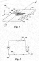
- the system 100 can include a first conductor, such as a first trace 102, and a second conductor, such as a second trace 104.
- the first trace 102 can connect, for example, to an input bus 106
- the second trace 104 can connect to an output bus 108.
- the input and output buses 106, 108 can connect to opposing sides of an energy source, such as a voltage source 110.
- a substrate 112 can include a major surface 114 that acts to support the traces 102, 104 and the buses 106, 108.
- the substrate 112 can include, for example, a silicon wafer, and the traces 102, 104 and/or buses 106, 108 can include metallizations (e.g. , copper) with thicknesses (perpendicular to the substrate) in the micrometer to nanometer range and lateral dimensions in the millimeter to nanometer range.
- metallizations e.g. , copper
- Multiple conduction paths 116 may form parallel electrical connections between opposing lengths of the first and second traces 102, 104.
- the first and second traces 102, 104 may be elongated along a length direction L that is parallel to the surface 114, and each of the conduction paths can respectively extend in a direction having a component orthogonal to the length direction.
- electrical power can be transmitted from the voltage source 110 through the input bus 106 to the first trace 102, and then through the conduction paths 116 to the second trace 104 and the output bus 108.
- the length along which the conduction paths 116 extend between opposing portions of the traces 102, 104 is referred to as the connection span 118. All of the conduction paths 116 can be configured to have respectively similar nominal electrical resistances. That is, assuming a similar configuration of the electrical input and output, each conduction path 116, analyzed individually, would be expected to exhibit a roughly similar electrical resistance.
- Each of the conduction paths 116 can respectively include a switch 120.
- Each switch 120 may, for example, be what is commonly referred to as microelectromechanical system (MEMS) switch.
- the MEMS switches 120 can respectively include cantilevers 122 that extend from anchor structures 124 that connect to one trace 102.
- the switches 120 (and the entireties of the conduction paths 116) can be formed of metal, such as copper.
- An actuation pad 126 can be configured to selectively receive an electrical charge, and can be disposed so as to cause, when charged, the cantilever 122 to be urged into contact with the other trace 104 due to an electrostatic force (this being referred to as the "closed" position of the switch, the alternative being the "open” position).
- the MEMS switches 120 can be substantially similar to one another.
- MEMS switches are relatively small in scale and often formed through standard microfabrication techniques that allow for batch processing of multiple switches that are all substantially similar in construction.
- the MEMS switches 120 can be configured to be actuated together, and in this way, power can be selectively provided from the voltage source 110 through the conduction paths 116, with the array of switches acting as a "switch element.”
- the traces 102, 104 can be configured to have respective cross-sectional areas A (taken transverse to the length direction L ) that decrease in opposing directions along the connection span 118.
- the traces 102, 104 may have constant thicknesses t (measured normally to the surface 114) and may have widths W (measured transversely to both the length direction L and the direction normal to the surface 114) that decrease in opposing directions along the connection span 118.
- the widths W of the traces 102, 104 may decrease continuously along the connection span 118.
- the traces can have a triangular shape (e.g.
- the widths W of the traces 102, 104 may decrease in discrete steps along the connection span 118.
- the shapes of the traces 102, 104 can be selected in a variety of ways to achieve the targeted decrease in cross sectional area A along the connection span 118, including utilizing traces of varying shape and/or thickness.
- electrical power can be transmitted from the voltage source 110 through the input bus 106 to the first trace 102, and then through the switches 120 (when those switches are in the closed position) to the second trace 104 and the output bus 108.
- an electrical current I can flow along the same path.
- the first trace 102 can have a cross-sectional area that decreases in the direction of current flow along the connection span 118.
- the second trace 104 can have a cross-sectional area that increases in the direction of current flow along the connection span 118.
- Electrical distribution systems configured in accordance with the above description (e.g. , the electrical distribution system 100 of Fig. 1 ) may exhibit a more uniform distribution of electrical current therethrough than that exhibited by conventional electrical distribution systems.
- the system 200 can include a first trace 202 that is configured to receive electrical current from an input bus (not shown), and a second trace 204 that is configured to deliver electrical current to an output bus (not shown).
- the traces may be formed of a conductive material, such as metal ( e.g. , copper).
- the traces 202, 204 may have widths W and thicknesses (measured out of the page in Fig. 9 ) that are roughly uniform, such that the cross sectional areas of the traces are relatively constant.
- Multiple conduction paths 216 may form parallel electrical connections between opposing lengths of the first and second traces 202, 204. All of the conduction paths 216 can be configured to have respectively similar nominal electrical resistances (a typical scenario for conventional electrical distribution systems employing arrays of switches of similar construction).
- the conduction paths 216 can be formed, for example, of metal ( e.g., copper). Referring to Fig. 10 , in operation, current I can travel along the first trace 202, through the conduction paths 216, and then through the second trace 204.
- the resistivity of the conduction paths 216 is of about the same order of magnitude as that for the traces 202, 204 ( e.g ., where both the traces and conduction paths are formed of a metal such as copper), Applicants have discovered that current will tend to be distributed somewhat non-uniformly amongst the various conduction paths. This can limit the overall current carrying capacity of the array of conduction paths 216.
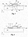
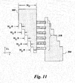
- FIG. 11 therein is shown an electrical distribution system 300 configured in accordance with another example embodiment.
- the electrical distribution system 300 can include traces 302, 304 and conduction paths 316 that connect the traces along a connection span 318.
- the traces 302, 304 can have constant thicknesses (measured out of the page in Fig. 11 ) and can have widths W that decrease in opposing directions along the connection span.
- the electrical distribution system 300 can have a number N of conduction paths (in Fig.
- a respective one of the traces 302, 304 can have a width W 0 .
- the traces 302, 304 can have widths that decrease by an amount W 0 / N when moving from one conduction path 316 to an adjacent conduction path along the connection span 318. For example, considering specific conduction paths 316a and 316b, the width of the first trace 302 decreases by W 0 /6 when moving from conduction path 316a to conduction path 316b, and the width of the second trace 304 decreases by W 0 /6 when moving from conduction path conduction path 316b to conduction path 316a.
- This decrease in trace width could be continuous along the connection span 318 ( e.g ., as depicted in Fig. 5 ) or could be accomplished in discrete increments (as shown in Fig. 11 ).
- Other rates of decrease of the cross-sectional area of the traces 302, 304 are also possible, and the rate chosen will depend on the electrical characteristics of the system 300 as well as any limitations on circuit layout ( e.g. , routing requirements where the electrical distribution system is part of an integrated circuit).
- the shaping of the traces 302, 304 to induce a more uniform distribution of current through the conduction paths 316 may become more important when the effective resistance of the conduction paths is smaller than or of the same order of magnitude as the traces. That is, where the conduction paths 316 present a relatively high resistance, current will flow quickly along the traces 302, 304 and will be distributed fairly evenly amongst the conduction paths. But, where the resistance presented by the conduction paths 316 is similar to or less than the resistance presented by the traces 302, 304, current may flow through the conduction paths without being fully distributed along the traces.
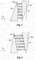
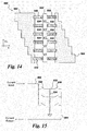
- the electrical distribution system 400 can include traces 402, 404 and conduction paths 416 that connect the traces along a connection span 418.
- Each of the conduction paths 416 can include a pair of switches, for example, substantially similar MEMS switches 420.
- the MEMS switches 420 can respectively include cantilevers 422 that extend from anchor structures 424.
- each conduction path 416 can be electrically connected in series ( e.g. , in the "back-to-back" configuration depicted in Fig. 13 , wherein the anchor structures 424 are included in an intermediate conductor 432) and configured to be actuated together.
- the intermediate conductor 432 can serve to respectively interconnect the various MEMS switches 420, and can also selectively ( e.g. , through a switch) connect to ground (connection not shown) to avoid the accumulation of electrical charge in the conduction paths 416 when both switches 420 are open, each of the conduction paths 416 is electrically isolated from the traces 402, 404 and the balance of the electrical distribution system 400. Referring to Figs.
- each pair of MEMS switches 520 that extends between traces 502, 504 can be interconnected by a respective intermediate conductor 532, with adjacent intermediate conductors being electrically connected by regions of increased resistance 534.
- regions of increased resistance 534 By introducing the regions of increased resistance 534, a majority of the current can be directed through the traces 502, 504, rather than through the intermediate conductors 532, when the switches 520 are in the closed position.
- many of the various components of the electrical distribution system 100 may be formed via standard microfabrication techniques, including thin film deposition and/or growth, photolithography, and film patterning through preferential growth and/or etching.
- standard microfabrication techniques including thin film deposition and/or growth, photolithography, and film patterning through preferential growth and/or etching.
- a process for fabricating the electrical distribution system 100 can begin by depositing, for example, via physical or chemical vapor deposition, a film 140 on a substrate 112 ( e.g. , see Fig. 16 ).
- the film 140 may be a metal film, such as copper.
- the film 140 can be patterned, for example, via photolithography, to form first and second traces 102, 104 that have respective cross-sectional areas that decrease in opposing directions ( e.g. , see Fig. 17 ).
- Multiple MEMS switches 120 can be simultaneously microfabricated on the substrate, either prior to or subsequent to the traces 102, 104.
- a sacrificial layer 142 can be patterned ( e.g.
- a film 144 can be deposited over the sacrificial layer ( e.g. , see Fig. 19 ).
- the film 144 can be patterned to form the switches 120 ( e.g. , see Fig. 20 ), which can be configured to form parallel electrical connections along the connection span 118 between the first and second traces 102, 104.
- the sacrificial layer 142 can be removed ( e.g. , see Fig. 21 ).
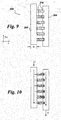
- an array of traces 602, 604 may be interconnected, with each set of adjacent traces 602, 604 being connected by multiple conduction paths 616 arranged as an array 650.
- Each of the conduction paths 616 can include a pair of switches 620 arranged in a back-to-back configuration.
- a single intermediate conductor 632 can serve to interconnect all of the switches 620 of all of the arrays 650.
Landscapes
- Physics & Mathematics (AREA)
- Electromagnetism (AREA)
- Micromachines (AREA)
- Design And Manufacture Of Integrated Circuits (AREA)
Applications Claiming Priority (1)
| Application Number | Priority Date | Filing Date | Title |
|---|---|---|---|
| US13/194,002 US8916996B2 (en) | 2011-07-29 | 2011-07-29 | Electrical distribution system |
Publications (2)
| Publication Number | Publication Date |
|---|---|
| EP2551866A1 EP2551866A1 (en) | 2013-01-30 |
| EP2551866B1 true EP2551866B1 (en) | 2014-04-02 |
Family
ID=47076046
Family Applications (1)
| Application Number | Title | Priority Date | Filing Date |
|---|---|---|---|
| EP12178134.8A Active EP2551866B1 (en) | 2011-07-29 | 2012-07-26 | Electrical distribution system |
Country Status (4)
| Country | Link |
|---|---|
| US (1) | US8916996B2 (ja) |
| EP (1) | EP2551866B1 (ja) |
| JP (1) | JP5973274B2 (ja) |
| CN (1) | CN102904168B (ja) |
Families Citing this family (5)
| Publication number | Priority date | Publication date | Assignee | Title |
|---|---|---|---|---|
| US10265086B2 (en) | 2014-06-30 | 2019-04-23 | Neuravi Limited | System for removing a clot from a blood vessel |
| US10413258B2 (en) | 2015-07-27 | 2019-09-17 | Koninklijke Philips N.V. | Medical placement alarm |
| ES2910600T3 (es) | 2019-03-04 | 2022-05-12 | Neuravi Ltd | Catéter de recuperación de coágulos accionado |
| US11944327B2 (en) | 2020-03-05 | 2024-04-02 | Neuravi Limited | Expandable mouth aspirating clot retrieval catheter |
| US11937839B2 (en) | 2021-09-28 | 2024-03-26 | Neuravi Limited | Catheter with electrically actuated expandable mouth |
Family Cites Families (19)
| Publication number | Priority date | Publication date | Assignee | Title |
|---|---|---|---|---|
| US4674180A (en) * | 1984-05-01 | 1987-06-23 | The Foxboro Company | Method of making a micromechanical electric shunt |
| US5587890A (en) * | 1994-08-08 | 1996-12-24 | Cooper Industries, Inc. | Vehicle electric power distribution system |
| AU2001253609A1 (en) | 2000-04-18 | 2001-10-30 | Standard Mems, Inc. | A micro relay |
| US6556099B2 (en) * | 2001-01-25 | 2003-04-29 | Motorola, Inc. | Multilayered tapered transmission line, device and method for making the same |
| AU2002355553A1 (en) * | 2001-08-07 | 2003-02-24 | Corporation For National Research Initiatives | An electromechanical switch and method of fabrication |
| US6876085B1 (en) * | 2001-09-24 | 2005-04-05 | Nortel Networks Limited | Signal layer interconnect using tapered traces |
| JP4278960B2 (ja) * | 2002-08-08 | 2009-06-17 | 富士通コンポーネント株式会社 | マイクロリレー及びマイクロリレーの製造方法 |
| US6832029B2 (en) * | 2002-12-17 | 2004-12-14 | Mcnc | Impedance control devices for use in the transition regions of electromagnetic and optical circuitry and methods for using the same |
| JP2004214112A (ja) * | 2003-01-08 | 2004-07-29 | Hitachi Ltd | マイクロマシンスイッチ |
| WO2004079855A1 (en) * | 2003-03-07 | 2004-09-16 | Ericsson Telecomunicações S.A. | Impedance-matching coupler |
| US8853001B2 (en) * | 2003-11-08 | 2014-10-07 | Stats Chippac, Ltd. | Semiconductor device and method of forming pad layout for flipchip semiconductor die |
| WO2005048314A2 (en) * | 2003-11-12 | 2005-05-26 | Silicon Pipe, Inc. | Tapered dielectric and conductor structures and applications thereof |
| WO2005117051A1 (ja) * | 2004-05-31 | 2005-12-08 | Yokohama Tlo Company Ltd. | マイクロマシンスイッチ |
| DE602005002330T2 (de) * | 2004-10-08 | 2008-05-29 | Alliant Techsystems Inc., Edina | Logarithmisch periodische Mikrostreifengruppenantenne mit geerdetem halbkoplanaren Übergang von Wellenleiter auf Mikrostreifenleitung |
| US7633725B2 (en) | 2005-12-20 | 2009-12-15 | General Electric Company | Micro-electromechanical system based soft switching |
| US7971193B2 (en) | 2006-07-14 | 2011-06-28 | Hewlett-Packard Development Company, L.P. | Methods for performining cross module context-sensitive security analysis |
| US7915696B2 (en) | 2007-10-24 | 2011-03-29 | General Electric Company | Electrical connection through a substrate to a microelectromechanical device |
| US7554222B2 (en) | 2007-11-01 | 2009-06-30 | General Electric Company | Micro-electromechanical system based switching |
| US8576029B2 (en) | 2010-06-17 | 2013-11-05 | General Electric Company | MEMS switching array having a substrate arranged to conduct switching current |
-
2011
- 2011-07-29 US US13/194,002 patent/US8916996B2/en active Active
-
2012
- 2012-07-25 JP JP2012164288A patent/JP5973274B2/ja active Active
- 2012-07-26 EP EP12178134.8A patent/EP2551866B1/en active Active
- 2012-07-27 CN CN201210263056.7A patent/CN102904168B/zh active Active
Also Published As
| Publication number | Publication date |
|---|---|
| US8916996B2 (en) | 2014-12-23 |
| US20130025934A1 (en) | 2013-01-31 |
| EP2551866A1 (en) | 2013-01-30 |
| JP5973274B2 (ja) | 2016-08-23 |
| CN102904168A (zh) | 2013-01-30 |
| JP2013232391A (ja) | 2013-11-14 |
| CN102904168B (zh) | 2017-08-08 |
Similar Documents
| Publication | Publication Date | Title |
|---|---|---|
| EP2551866B1 (en) | Electrical distribution system | |
| US7839028B2 (en) | Nanoelectromechanical systems and methods for making the same | |
| US20100015744A1 (en) | Micro-Electromechanical Device and Method of Making the Same | |
| WO2000024021A1 (en) | Micromechanical switching devices | |
| US7692519B2 (en) | MEMS switch with improved standoff voltage control | |
| US7346981B2 (en) | Method for fabricating microelectromechanical system (MEMS) devices | |
| US9443658B2 (en) | Variable capacitor compromising MEMS devices for radio frequency applications | |
| US6812810B2 (en) | Bridges for microelectromechanical structures | |
| US9123493B2 (en) | Microelectromechanical switches for steering of RF signals | |
| US10181837B2 (en) | Widely tunable cavity filter using low voltage, large out-of-plane actuation MEMS | |
| EP2239796A2 (en) | Method of fabricating a resistive switching element including nanogap electrodes | |
| KR101262606B1 (ko) | 커패시터 및 이의 제조방법 | |
| RU2541439C1 (ru) | Электростатический мэмс ключ | |
| WO2022218595A1 (de) | Mikroelektromechanisches schaltelement, vorrichtung und betriebsverfahren | |
| US20170271114A1 (en) | Printed mems switch | |
| WO2011016815A1 (en) | Nanotube esd protective devices and corresponding nonvolatile and volatile nanotube switches | |
| Angira et al. | Design and pull-in voltage optimization of series metal-to-metal contact RF MEMS switch | |
| KR20160003541U (ko) | 그래핀의 굽힘변형, 위치이동, 중 하나 이상 선택되는 것을 이용하여 하나 이상의 일 함수를 하나 이상 조절하는 트랜지스터 | |
| KR20150084695A (ko) | 그래핀의 굽힘변형, 위치이동, 중 하나 이상 선택되는 것을 이용하여 하나 이상의 일 함수를 하나 이상 조절하는 트랜지스터 | |
| TW201521349A (zh) | 用於微機電系統裝置之控制電路繞線組態 | |
| JP2008283473A (ja) | 電力増幅器 |
Legal Events
| Date | Code | Title | Description |
|---|---|---|---|
| PUAI | Public reference made under article 153(3) epc to a published international application that has entered the european phase |
Free format text: ORIGINAL CODE: 0009012 |
|
| AK | Designated contracting states |
Kind code of ref document: A1 Designated state(s): AL AT BE BG CH CY CZ DE DK EE ES FI FR GB GR HR HU IE IS IT LI LT LU LV MC MK MT NL NO PL PT RO RS SE SI SK SM TR |
|
| AX | Request for extension of the european patent |
Extension state: BA ME |
|
| 17P | Request for examination filed |
Effective date: 20130730 |
|
| RBV | Designated contracting states (corrected) |
Designated state(s): AL AT BE BG CH CY CZ DE DK EE ES FI FR GB GR HR HU IE IS IT LI LT LU LV MC MK MT NL NO PL PT RO RS SE SI SK SM TR |
|
| GRAP | Despatch of communication of intention to grant a patent |
Free format text: ORIGINAL CODE: EPIDOSNIGR1 |
|
| RIC1 | Information provided on ipc code assigned before grant |
Ipc: H01H 1/58 20060101ALI20131104BHEP Ipc: H01H 1/00 20060101AFI20131104BHEP Ipc: B81B 7/00 20060101ALI20131104BHEP Ipc: H01H 59/00 20060101ALN20131104BHEP Ipc: H01H 9/40 20060101ALI20131104BHEP |
|
| INTG | Intention to grant announced |
Effective date: 20131125 |
|
| GRAS | Grant fee paid |
Free format text: ORIGINAL CODE: EPIDOSNIGR3 |
|
| GRAA | (expected) grant |
Free format text: ORIGINAL CODE: 0009210 |
|
| AK | Designated contracting states |
Kind code of ref document: B1 Designated state(s): AL AT BE BG CH CY CZ DE DK EE ES FI FR GB GR HR HU IE IS IT LI LT LU LV MC MK MT NL NO PL PT RO RS SE SI SK SM TR |
|
| REG | Reference to a national code |
Ref country code: GB Ref legal event code: FG4D |
|
| REG | Reference to a national code |
Ref country code: AT Ref legal event code: REF Ref document number: 660558 Country of ref document: AT Kind code of ref document: T Effective date: 20140415 Ref country code: CH Ref legal event code: EP |
|
| REG | Reference to a national code |
Ref country code: IE Ref legal event code: FG4D |
|
| REG | Reference to a national code |
Ref country code: DE Ref legal event code: R096 Ref document number: 602012001276 Country of ref document: DE Effective date: 20140508 |
|
| REG | Reference to a national code |
Ref country code: AT Ref legal event code: MK05 Ref document number: 660558 Country of ref document: AT Kind code of ref document: T Effective date: 20140402 |
|
| REG | Reference to a national code |
Ref country code: NL Ref legal event code: VDEP Effective date: 20140402 |
|
| REG | Reference to a national code |
Ref country code: LT Ref legal event code: MG4D |
|
| PG25 | Lapsed in a contracting state [announced via postgrant information from national office to epo] |
Ref country code: NO Free format text: LAPSE BECAUSE OF FAILURE TO SUBMIT A TRANSLATION OF THE DESCRIPTION OR TO PAY THE FEE WITHIN THE PRESCRIBED TIME-LIMIT Effective date: 20140702 Ref country code: CY Free format text: LAPSE BECAUSE OF FAILURE TO SUBMIT A TRANSLATION OF THE DESCRIPTION OR TO PAY THE FEE WITHIN THE PRESCRIBED TIME-LIMIT Effective date: 20140402 Ref country code: FI Free format text: LAPSE BECAUSE OF FAILURE TO SUBMIT A TRANSLATION OF THE DESCRIPTION OR TO PAY THE FEE WITHIN THE PRESCRIBED TIME-LIMIT Effective date: 20140402 Ref country code: CZ Free format text: LAPSE BECAUSE OF FAILURE TO SUBMIT A TRANSLATION OF THE DESCRIPTION OR TO PAY THE FEE WITHIN THE PRESCRIBED TIME-LIMIT Effective date: 20140402 Ref country code: GR Free format text: LAPSE BECAUSE OF FAILURE TO SUBMIT A TRANSLATION OF THE DESCRIPTION OR TO PAY THE FEE WITHIN THE PRESCRIBED TIME-LIMIT Effective date: 20140703 Ref country code: BG Free format text: LAPSE BECAUSE OF FAILURE TO SUBMIT A TRANSLATION OF THE DESCRIPTION OR TO PAY THE FEE WITHIN THE PRESCRIBED TIME-LIMIT Effective date: 20140702 Ref country code: NL Free format text: LAPSE BECAUSE OF FAILURE TO SUBMIT A TRANSLATION OF THE DESCRIPTION OR TO PAY THE FEE WITHIN THE PRESCRIBED TIME-LIMIT Effective date: 20140402 Ref country code: IS Free format text: LAPSE BECAUSE OF FAILURE TO SUBMIT A TRANSLATION OF THE DESCRIPTION OR TO PAY THE FEE WITHIN THE PRESCRIBED TIME-LIMIT Effective date: 20140802 Ref country code: LT Free format text: LAPSE BECAUSE OF FAILURE TO SUBMIT A TRANSLATION OF THE DESCRIPTION OR TO PAY THE FEE WITHIN THE PRESCRIBED TIME-LIMIT Effective date: 20140402 |
|
| PGFP | Annual fee paid to national office [announced via postgrant information from national office to epo] |
Ref country code: DE Payment date: 20140729 Year of fee payment: 3 |
|
| PG25 | Lapsed in a contracting state [announced via postgrant information from national office to epo] |
Ref country code: HR Free format text: LAPSE BECAUSE OF FAILURE TO SUBMIT A TRANSLATION OF THE DESCRIPTION OR TO PAY THE FEE WITHIN THE PRESCRIBED TIME-LIMIT Effective date: 20140402 Ref country code: AT Free format text: LAPSE BECAUSE OF FAILURE TO SUBMIT A TRANSLATION OF THE DESCRIPTION OR TO PAY THE FEE WITHIN THE PRESCRIBED TIME-LIMIT Effective date: 20140402 Ref country code: LV Free format text: LAPSE BECAUSE OF FAILURE TO SUBMIT A TRANSLATION OF THE DESCRIPTION OR TO PAY THE FEE WITHIN THE PRESCRIBED TIME-LIMIT Effective date: 20140402 Ref country code: SE Free format text: LAPSE BECAUSE OF FAILURE TO SUBMIT A TRANSLATION OF THE DESCRIPTION OR TO PAY THE FEE WITHIN THE PRESCRIBED TIME-LIMIT Effective date: 20140402 Ref country code: RS Free format text: LAPSE BECAUSE OF FAILURE TO SUBMIT A TRANSLATION OF THE DESCRIPTION OR TO PAY THE FEE WITHIN THE PRESCRIBED TIME-LIMIT Effective date: 20140402 Ref country code: PL Free format text: LAPSE BECAUSE OF FAILURE TO SUBMIT A TRANSLATION OF THE DESCRIPTION OR TO PAY THE FEE WITHIN THE PRESCRIBED TIME-LIMIT Effective date: 20140402 Ref country code: ES Free format text: LAPSE BECAUSE OF FAILURE TO SUBMIT A TRANSLATION OF THE DESCRIPTION OR TO PAY THE FEE WITHIN THE PRESCRIBED TIME-LIMIT Effective date: 20140402 |
|
| PG25 | Lapsed in a contracting state [announced via postgrant information from national office to epo] |
Ref country code: PT Free format text: LAPSE BECAUSE OF FAILURE TO SUBMIT A TRANSLATION OF THE DESCRIPTION OR TO PAY THE FEE WITHIN THE PRESCRIBED TIME-LIMIT Effective date: 20140804 |
|
| REG | Reference to a national code |
Ref country code: DE Ref legal event code: R097 Ref document number: 602012001276 Country of ref document: DE |
|
| PG25 | Lapsed in a contracting state [announced via postgrant information from national office to epo] |
Ref country code: DK Free format text: LAPSE BECAUSE OF FAILURE TO SUBMIT A TRANSLATION OF THE DESCRIPTION OR TO PAY THE FEE WITHIN THE PRESCRIBED TIME-LIMIT Effective date: 20140402 Ref country code: SK Free format text: LAPSE BECAUSE OF FAILURE TO SUBMIT A TRANSLATION OF THE DESCRIPTION OR TO PAY THE FEE WITHIN THE PRESCRIBED TIME-LIMIT Effective date: 20140402 Ref country code: EE Free format text: LAPSE BECAUSE OF FAILURE TO SUBMIT A TRANSLATION OF THE DESCRIPTION OR TO PAY THE FEE WITHIN THE PRESCRIBED TIME-LIMIT Effective date: 20140402 Ref country code: RO Free format text: LAPSE BECAUSE OF FAILURE TO SUBMIT A TRANSLATION OF THE DESCRIPTION OR TO PAY THE FEE WITHIN THE PRESCRIBED TIME-LIMIT Effective date: 20140402 Ref country code: BE Free format text: LAPSE BECAUSE OF FAILURE TO SUBMIT A TRANSLATION OF THE DESCRIPTION OR TO PAY THE FEE WITHIN THE PRESCRIBED TIME-LIMIT Effective date: 20140402 |
|
| PLBE | No opposition filed within time limit |
Free format text: ORIGINAL CODE: 0009261 |
|
| STAA | Information on the status of an ep patent application or granted ep patent |
Free format text: STATUS: NO OPPOSITION FILED WITHIN TIME LIMIT |
|
| PG25 | Lapsed in a contracting state [announced via postgrant information from national office to epo] |
Ref country code: LU Free format text: LAPSE BECAUSE OF FAILURE TO SUBMIT A TRANSLATION OF THE DESCRIPTION OR TO PAY THE FEE WITHIN THE PRESCRIBED TIME-LIMIT Effective date: 20140726 |
|
| 26N | No opposition filed |
Effective date: 20150106 |
|
| REG | Reference to a national code |
Ref country code: DE Ref legal event code: R097 Ref document number: 602012001276 Country of ref document: DE Effective date: 20150106 |
|
| REG | Reference to a national code |
Ref country code: IE Ref legal event code: MM4A |
|
| PG25 | Lapsed in a contracting state [announced via postgrant information from national office to epo] |
Ref country code: RS Free format text: LAPSE BECAUSE OF FAILURE TO SUBMIT A TRANSLATION OF THE DESCRIPTION OR TO PAY THE FEE WITHIN THE PRESCRIBED TIME-LIMIT Effective date: 20141119 |
|
| PG25 | Lapsed in a contracting state [announced via postgrant information from national office to epo] |
Ref country code: SI Free format text: LAPSE BECAUSE OF FAILURE TO SUBMIT A TRANSLATION OF THE DESCRIPTION OR TO PAY THE FEE WITHIN THE PRESCRIBED TIME-LIMIT Effective date: 20140402 |
|
| PG25 | Lapsed in a contracting state [announced via postgrant information from national office to epo] |
Ref country code: IE Free format text: LAPSE BECAUSE OF NON-PAYMENT OF DUE FEES Effective date: 20140726 |
|
| REG | Reference to a national code |
Ref country code: DE Ref legal event code: R119 Ref document number: 602012001276 Country of ref document: DE |
|
| REG | Reference to a national code |
Ref country code: CH Ref legal event code: PL |
|
| PG25 | Lapsed in a contracting state [announced via postgrant information from national office to epo] |
Ref country code: DE Free format text: LAPSE BECAUSE OF NON-PAYMENT OF DUE FEES Effective date: 20160202 Ref country code: MC Free format text: LAPSE BECAUSE OF FAILURE TO SUBMIT A TRANSLATION OF THE DESCRIPTION OR TO PAY THE FEE WITHIN THE PRESCRIBED TIME-LIMIT Effective date: 20140402 Ref country code: SM Free format text: LAPSE BECAUSE OF FAILURE TO SUBMIT A TRANSLATION OF THE DESCRIPTION OR TO PAY THE FEE WITHIN THE PRESCRIBED TIME-LIMIT Effective date: 20140402 Ref country code: LI Free format text: LAPSE BECAUSE OF NON-PAYMENT OF DUE FEES Effective date: 20150731 Ref country code: CH Free format text: LAPSE BECAUSE OF NON-PAYMENT OF DUE FEES Effective date: 20150731 |
|
| PG25 | Lapsed in a contracting state [announced via postgrant information from national office to epo] |
Ref country code: MT Free format text: LAPSE BECAUSE OF FAILURE TO SUBMIT A TRANSLATION OF THE DESCRIPTION OR TO PAY THE FEE WITHIN THE PRESCRIBED TIME-LIMIT Effective date: 20140402 |
|
| REG | Reference to a national code |
Ref country code: FR Ref legal event code: PLFP Year of fee payment: 5 |
|
| PG25 | Lapsed in a contracting state [announced via postgrant information from national office to epo] |
Ref country code: HU Free format text: LAPSE BECAUSE OF FAILURE TO SUBMIT A TRANSLATION OF THE DESCRIPTION OR TO PAY THE FEE WITHIN THE PRESCRIBED TIME-LIMIT; INVALID AB INITIO Effective date: 20120726 Ref country code: TR Free format text: LAPSE BECAUSE OF FAILURE TO SUBMIT A TRANSLATION OF THE DESCRIPTION OR TO PAY THE FEE WITHIN THE PRESCRIBED TIME-LIMIT Effective date: 20140402 |
|
| REG | Reference to a national code |
Ref country code: FR Ref legal event code: PLFP Year of fee payment: 6 |
|
| REG | Reference to a national code |
Ref country code: FR Ref legal event code: PLFP Year of fee payment: 7 |
|
| PG25 | Lapsed in a contracting state [announced via postgrant information from national office to epo] |
Ref country code: MK Free format text: LAPSE BECAUSE OF FAILURE TO SUBMIT A TRANSLATION OF THE DESCRIPTION OR TO PAY THE FEE WITHIN THE PRESCRIBED TIME-LIMIT Effective date: 20140402 |
|
| PG25 | Lapsed in a contracting state [announced via postgrant information from national office to epo] |
Ref country code: AL Free format text: LAPSE BECAUSE OF FAILURE TO SUBMIT A TRANSLATION OF THE DESCRIPTION OR TO PAY THE FEE WITHIN THE PRESCRIBED TIME-LIMIT Effective date: 20140402 |
|
| PGFP | Annual fee paid to national office [announced via postgrant information from national office to epo] |
Ref country code: IT Payment date: 20230620 Year of fee payment: 12 Ref country code: FR Payment date: 20230621 Year of fee payment: 12 |
|
| PGFP | Annual fee paid to national office [announced via postgrant information from national office to epo] |
Ref country code: GB Payment date: 20230620 Year of fee payment: 12 |