EP2549492A1 - High power inductors using a magnetic basis - Google Patents
High power inductors using a magnetic basis Download PDFInfo
- Publication number
- EP2549492A1 EP2549492A1 EP12180116A EP12180116A EP2549492A1 EP 2549492 A1 EP2549492 A1 EP 2549492A1 EP 12180116 A EP12180116 A EP 12180116A EP 12180116 A EP12180116 A EP 12180116A EP 2549492 A1 EP2549492 A1 EP 2549492A1
- Authority
- EP
- European Patent Office
- Prior art keywords
- ferromagnetic plate
- inductor
- biased
- magnetic
- adhesive
- Prior art date
- Legal status (The legal status is an assumption and is not a legal conclusion. Google has not performed a legal analysis and makes no representation as to the accuracy of the status listed.)
- Withdrawn
Links
- 230000005291 magnetic effect Effects 0.000 title claims abstract description 53
- 230000005294 ferromagnetic effect Effects 0.000 claims abstract description 95
- 239000000853 adhesive Substances 0.000 claims abstract description 30
- 230000001070 adhesive effect Effects 0.000 claims abstract description 30
- 239000004020 conductor Substances 0.000 claims abstract description 30
- 239000000843 powder Substances 0.000 claims abstract description 30
- 230000004907 flux Effects 0.000 claims description 25
- 239000000696 magnetic material Substances 0.000 claims description 11
- 229910000859 α-Fe Inorganic materials 0.000 claims description 10
- 229910052761 rare earth metal Inorganic materials 0.000 claims description 9
- 150000002910 rare earth metals Chemical class 0.000 claims description 9
- RYGMFSIKBFXOCR-UHFFFAOYSA-N Copper Chemical compound [Cu] RYGMFSIKBFXOCR-UHFFFAOYSA-N 0.000 claims description 7
- 229910052802 copper Inorganic materials 0.000 claims description 7
- 239000010949 copper Substances 0.000 claims description 7
- 239000004593 Epoxy Substances 0.000 claims description 6
- 239000002313 adhesive film Substances 0.000 claims description 6
- 229910045601 alloy Inorganic materials 0.000 claims description 4
- 239000000956 alloy Substances 0.000 claims description 4
- QJVKUMXDEUEQLH-UHFFFAOYSA-N [B].[Fe].[Nd] Chemical compound [B].[Fe].[Nd] QJVKUMXDEUEQLH-UHFFFAOYSA-N 0.000 claims description 3
- 229910001172 neodymium magnet Inorganic materials 0.000 claims description 3
- 229910000938 samarium–cobalt magnet Inorganic materials 0.000 claims description 3
- KPLQYGBQNPPQGA-UHFFFAOYSA-N cobalt samarium Chemical compound [Co].[Sm] KPLQYGBQNPPQGA-UHFFFAOYSA-N 0.000 claims description 2
- 239000006247 magnetic powder Substances 0.000 claims description 2
- 238000000034 method Methods 0.000 abstract description 13
- 239000000203 mixture Substances 0.000 abstract description 13
- 230000008901 benefit Effects 0.000 description 6
- XEEYBQQBJWHFJM-UHFFFAOYSA-N Iron Chemical compound [Fe] XEEYBQQBJWHFJM-UHFFFAOYSA-N 0.000 description 5
- 239000000463 material Substances 0.000 description 5
- 239000003302 ferromagnetic material Substances 0.000 description 3
- 239000000654 additive Substances 0.000 description 2
- 230000000996 additive effect Effects 0.000 description 2
- 239000000919 ceramic Substances 0.000 description 2
- 230000007423 decrease Effects 0.000 description 2
- 230000001965 increasing effect Effects 0.000 description 2
- 229910052742 iron Inorganic materials 0.000 description 2
- 238000004519 manufacturing process Methods 0.000 description 2
- 239000002245 particle Substances 0.000 description 2
- 238000007650 screen-printing Methods 0.000 description 2
- 230000005465 channeling Effects 0.000 description 1
- 230000005347 demagnetization Effects 0.000 description 1
- 230000009977 dual effect Effects 0.000 description 1
- 230000001939 inductive effect Effects 0.000 description 1
- 230000001788 irregular Effects 0.000 description 1
- -1 molypermalloy (MPP) Inorganic materials 0.000 description 1
- 239000012256 powdered iron Substances 0.000 description 1
- 238000009738 saturating Methods 0.000 description 1
- 229910000702 sendust Inorganic materials 0.000 description 1
- 239000007779 soft material Substances 0.000 description 1
- 230000003068 static effect Effects 0.000 description 1
Images


Classifications
-
- H—ELECTRICITY
- H01—ELECTRIC ELEMENTS
- H01F—MAGNETS; INDUCTANCES; TRANSFORMERS; SELECTION OF MATERIALS FOR THEIR MAGNETIC PROPERTIES
- H01F3/00—Cores, Yokes, or armatures
- H01F3/10—Composite arrangements of magnetic circuits
- H01F3/14—Constrictions; Gaps, e.g. air-gaps
-
- H—ELECTRICITY
- H01—ELECTRIC ELEMENTS
- H01F—MAGNETS; INDUCTANCES; TRANSFORMERS; SELECTION OF MATERIALS FOR THEIR MAGNETIC PROPERTIES
- H01F17/00—Fixed inductances of the signal type
- H01F17/04—Fixed inductances of the signal type with magnetic core
- H01F17/043—Fixed inductances of the signal type with magnetic core with two, usually identical or nearly identical parts enclosing completely the coil (pot cores)
-
- H—ELECTRICITY
- H01—ELECTRIC ELEMENTS
- H01F—MAGNETS; INDUCTANCES; TRANSFORMERS; SELECTION OF MATERIALS FOR THEIR MAGNETIC PROPERTIES
- H01F27/00—Details of transformers or inductances, in general
- H01F27/28—Coils; Windings; Conductive connections
- H01F27/2847—Sheets; Strips
-
- Y—GENERAL TAGGING OF NEW TECHNOLOGICAL DEVELOPMENTS; GENERAL TAGGING OF CROSS-SECTIONAL TECHNOLOGIES SPANNING OVER SEVERAL SECTIONS OF THE IPC; TECHNICAL SUBJECTS COVERED BY FORMER USPC CROSS-REFERENCE ART COLLECTIONS [XRACs] AND DIGESTS
- Y10—TECHNICAL SUBJECTS COVERED BY FORMER USPC
- Y10T—TECHNICAL SUBJECTS COVERED BY FORMER US CLASSIFICATION
- Y10T29/00—Metal working
- Y10T29/49—Method of mechanical manufacture
- Y10T29/49002—Electrical device making
- Y10T29/4902—Electromagnet, transformer or inductor
- Y10T29/49073—Electromagnet, transformer or inductor by assembling coil and core
Definitions
- Low profile inductors commonly defined as inductors having a profile less than about 10 mm are in existence today in the form of ferrites with unique geometries and pressed iron powder around a wound coil. Ferrite based low profile inductors have an inherent limitation of magnetic saturation at relatively low levels of current. When magnetic saturation occurs, inductance value decreases dramatically.
- Pressed iron inductors allow for much higher input current than ferrite inductors, but have the limitation of producing high core losses at high frequencies (such as frequencies greater than 200 kHz). What is needed is an efficient means to provide inductance at high frequencies allowing high input currents.
- Another object, feature, or advantage of the present invention is to use adhesive film thickness or magnet particle size to adjust inductance characteristics.
- a further object, feature, or advantage of the present invention is to increase the capability of an inductor to effectively handle more DC while maintaining inductance.
- a biased gap inductor includes a first ferromagnetic plate, a second ferromagnetic plate, a conductor sandwiched between the first ferromagnetic plate and the second ferromagnetic plate, and an adhesive between the first ferromagnetic plate and the second ferromagnetic plate, the adhesive comprising magnetically hard magnet powder to thereby form at least one magnetic gap.
- the adhesive has a thickness of less than 500 um and preferably less than 100 um.
- the magnetic powder size can be used to set the inductance level of the part. Also the amount of magnet powder can modify characteristics of the part to produce a desired performance.
- a method of forming an inductor includes providing a first ferromagnetic plate and a second ferromagnetic plate and a conductor, placing the conductor between the first ferromagnetic plate and the second ferromagnetic plate, adhering the first ferromagnetic plate to the second ferromagnetic plate with a composition comprising an adhesive and a magnet powder to form magnetic gaps, and magnetizing the inductor.
- the composition has a thickness of less than 500 um and preferably less than 100 um.
- a biased gap inductor includes a first ferromagnetic plate and a second ferromagnetic plate.
- a conductor is sandwiched between the first ferromagnetic plate and the second ferromagnetic plate.
- a magnetic material having a thickness of less than 100 um is between the first ferromagnetic plate and the second ferromagnetic plate to from at least one magnetic gap. The thickness may be used to define inductance characteristics of the inductor.
- FIG. 1 illustrates a prior art device where a single strip of copper can be placed between two ferrite parts to create an inductor. While this is effective in creating low value, high frequency inductors, it limits the amount of input current the inductor can handle without saturating. The primary cause of saturation comes from the fact that all magnetic flux induced by the copper flows through narrow cross-sectional areas.
- FIG. 1 illustrates the flux pattern in a single copper strip inductor.
- an inductor 10 has a first ferromagnetic plate 12 and a second ferromagnetic plate 14. There is a spacing 16 between the first ferromagnetic plate 12 and the second ferromagnetic plate 14.
- the magnetic flux induced by a current through the single strip copper conductor 18 is split between each plate 12, 14. Input current 20 is shown using notation to indicate that the current is flowing into the page. Arrows 22, 24, 26, 28 indicate the direction of magnetic flux induced by the current 20 through the conductor 18. Note that all the magnetic flux induced by the current in the copper conductor 18 flows through narrow cross-sectional 22, 26 areas thereby becoming the primary cause of saturation.
- FIG. 2 illustrates one embodiment of the present invention.
- An inductor 30 is shown which is formed from a first ferromagnetic plate 12 and a second ferromagnetic plate 14.
- the first ferromagnetic plate 12 and the second ferromagnetic plate 14 are mechanically bonded through a composition 32 which includes an adhesive and a magnet powder.
- Arrows 22, 26, 38, 40 indicate the direction of magnetic flux induced by the current 20 through the conductor 18.
- Arrows 34, 36, 42, 44 indicate the direction of magnet induced "counter" flux.
- the composition 32 may be comprised of epoxy and magnet powder mixed in predetermined ratios.
- the use of the adhesive with the magnet powder has a dual role in the assembly of an inductive component. Varying the size of the magnet particulate raises or lowers the inductance of the part. Small magnet powder size creates a thin gap inductor with a high inductance level. A large magnet powder increases the gap size resulting in a reduced inductance of a part.
- the magnet powder particulate size can be selected to tailor the inductance of a part for a specific application. In other words, the magnet powder size can be used to set the inductance level of the part. Also, the amount of magnet powder used can modify characteristics of the part to produce a desired performance.
- the second role of the adhesive is to permanently bind the parts together making the assembly robust to mechanical loads.
- the thickness of the magnet particulate layer is between about 0 to 100 um. Larger magnetic bias thickness of between about 0 and 500 may also be used.
- the magnet powder can consist of a spherical or irregular shaped material. Ceramic magnet powders can be used as the magnet powder.
- the preferred materials are spherical rare earth magnetic material such as, but not limited to, Neodymium-Iron-Boron or Samarium-Cobalt magnet powder.
- Neodymium-Iron-Boron or Samarium-Cobalt magnet powder.
- Ferromagnetic plates can be made from a magnetically soft material such as, without limitation, ferrite, molypermalloy (MPP), Sendust, Hi Flux, or pressed iron. Although other materials may be used, a preferred material is ferrite as it has low core losses at high frequencies and is generally less expensive than alternatives. Ferrite has low magnetic saturation resistance and thus benefits from introducing a magnetic bias.
- MPP molypermalloy
- Sendust Sendust
- Hi Flux or pressed iron.
- a preferred material is ferrite as it has low core losses at high frequencies and is generally less expensive than alternatives. Ferrite has low magnetic saturation resistance and thus benefits from introducing a magnetic bias.
- the present invention provides for adding magnet powder filled adhesive between ferromagnetic plates. Once the adhesive is fully cured, the component is magnetized such that the magnetic material applies a steady state magnetic flux field that opposes the direction induced from a current carrying inductor.
- FIG. 2 illustrates the static magnetic flux and the induced magnetic flux from the conductor.
- FIG. 3 is a hypothetical B-H loop of soft ferromagnetic ferrite plates.
- the ferromagnetic material is polarized or biased such that its flux field is near the maximum negative saturation point. When DC is applied, this negative flux field gradually decreases until the magnetic flux density in the ferromagnetic material is zero. Upon further increase in DC, the magnetic flux field begins to go positive until magnetic saturation occurs. Introducing magnetic material in the gap thus increases the ferromagnetic material's ability to withstand saturation thereby significantly increasing its range, such as by two times.
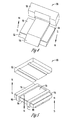
- FIG. 4 is a perspective view of a single conductor inductor 50 with two magnetic gaps.
- two ferromagnetic plates 52, 53 are combined together by a distance set by the size of the magnetic particulate.
- a mixture of magnet powder and epoxy forms the composition 56 which may be screen printed onto one of the sides of the ferromagnetic plates, ferromagnetic plate 52 as shown in FIG. 4 .
- a magnetic gap is created in each region where the composition 56 is applied.
- a second ferromagnetic plate 53 is placed upon the first and the adhesive is heat cured to permanently bond the assembly together. Once the parts are cured, they are then magnetized.
- FIG. 4 is a perspective view of a single conductor inductor 50 with two magnetic gaps.
- two ferromagnetic plates 52, 53 are combined together by a distance set by the size of the magnetic particulate.
- a mixture of magnet powder and epoxy forms the composition 56 which may be screen printed onto one of the sides of the ferromagnetic plates, ferromagnetic plate 52
- FIG. 4 illustrates the polarity of the magnetic material such that the subsequent flux field between the two ferromagnetic plates adds to each others magnetic flux direction.
- the polarity of the magnet induced flux is set in the opposite direction to any magnetic induced flux caused from direct current input into the conductor.
- FIG. 5 is a perspective view of one embodiment where there are three magnetic gaps, each of the magnetic gaps formed for a mixture containing magnet powder and preferably an adhesive such as epoxy.
- the mixture can be deposited by screen printing and can be considered a magnetic film as it includes a magnet powder is applied in three separate places, 70A, 70B, 70C.
- the outside magnetic films 70A, 70B are polarized in the same direction while the center 70C is polarized in an opposite direction. This is performed in order to form a magnetic field that will be additive for all three magnetic films.
- the inductor 60 include a first ferromagnetic plate 62 and a second ferromagnetic plate 64. There are grooves 63 cut in ferromagnetic plate 62.
- the grooves 63 extend from one side of the ferromagnetic plate 62 to an opposite side of the ferromagnetic plate 62.
- a conductor 65 is shown.
- the conductor 65 which includes segments 66, 68 on the side of the second ferromagnetic plate 64 is bent around the second ferromagnetic plate 64 to form three surfaces 70A, 70B, 70C upon each of which the magnetic film is adhered.
- the adhesive may be heat cured, then device 60 may be magnetized.
- FIG. 5 provides a multi-poled configuration as the outside magnetic films are polarized in the same direction while the center is polarized in an opposite direction. This is done to form a magnetic field that will be additive for all three magnetic films.
- the polarity of the magnet induced flux is set in the opposite direction to any magnetic induced flux caused from direct current input into the conductor.
- the present invention provides for improved inductors and methods of manufacturing the same.
- the present invention contemplates numerous variations in the types of materials used, manufacturing techniques applied, and other variations which are within the spirit and scope of the invention.
Abstract
A biased gap inductor includes a first ferromagnetic plate, a second ferromagnetic plate, a conductor sandwiched between the first ferromagnetic plate and the second ferromagnetic plate, and an adhesive between the first ferromagnetic plate and the second ferromagnetic plate, the adhesive comprising magnet powder to thereby form at least one magnetic gap. A method of forming an inductor includes providing a first ferromagnetic plate and a second ferromagnetic plate and a conductor, placing the conductor between the first ferromagnetic plate and the second ferromagnetic plate, adhering the first ferromagnetic plate to the second ferromagnetic plate with a composition comprising an adhesive and a magnet powder to form magnetic gaps, and magnetizing the inductor.
Description
- This application claims priority under 35 U.S.C. § 119 to provisional application Serial No.
60/970,578 filed September 7, 2007 - Low profile inductors, commonly defined as inductors having a profile less than about 10 mm are in existence today in the form of ferrites with unique geometries and pressed iron powder around a wound coil. Ferrite based low profile inductors have an inherent limitation of magnetic saturation at relatively low levels of current. When magnetic saturation occurs, inductance value decreases dramatically.
- Pressed iron inductors allow for much higher input current than ferrite inductors, but have the limitation of producing high core losses at high frequencies (such as frequencies greater than 200 kHz). What is needed is an efficient means to provide inductance at high frequencies allowing high input currents.
- It is therefore a primary, object, feature, or advantage of the present invention to improve upon the state of the art.
- It is a further object, feature, or advantage of the present invention to provide an inductor which has lower core losses at high ripple currents (> 5 A) and frequencies (> 200 kHz) in a thin package yet also have the high saturation current performance of powdered iron.
- Another object, feature, or advantage of the present invention is to use adhesive film thickness or magnet particle size to adjust inductance characteristics.
- A further object, feature, or advantage of the present invention is to increase the capability of an inductor to effectively handle more DC while maintaining inductance.
- One or more of these and/or other objects, features, or advantages of the present invention will become apparent from the description of the invention that follows.
- According to one aspect of the present invention, a biased gap inductor includes a first ferromagnetic plate, a second ferromagnetic plate, a conductor sandwiched between the first ferromagnetic plate and the second ferromagnetic plate, and an adhesive between the first ferromagnetic plate and the second ferromagnetic plate, the adhesive comprising magnetically hard magnet powder to thereby form at least one magnetic gap. The adhesive has a thickness of less than 500 um and preferably less than 100 um. The magnetic powder size can be used to set the inductance level of the part. Also the amount of magnet powder can modify characteristics of the part to produce a desired performance.
- According to another aspect of the present invention, a method of forming an inductor includes providing a first ferromagnetic plate and a second ferromagnetic plate and a conductor, placing the conductor between the first ferromagnetic plate and the second ferromagnetic plate, adhering the first ferromagnetic plate to the second ferromagnetic plate with a composition comprising an adhesive and a magnet powder to form magnetic gaps, and magnetizing the inductor. The composition has a thickness of less than 500 um and preferably less than 100 um.
- According to another aspect of the present invention, a biased gap inductor is provided. The inductor includes a first ferromagnetic plate and a second ferromagnetic plate. A conductor is sandwiched between the first ferromagnetic plate and the second ferromagnetic plate. A magnetic material having a thickness of less than 100 um is between the first ferromagnetic plate and the second ferromagnetic plate to from at least one magnetic gap. The thickness may be used to define inductance characteristics of the inductor.
-
-
FIG. 1 is a cross-section of a prior art inductor without flux channeling. -
FIG. 2 is a cross-section of one embodiment of a flux-channeled inductor of the present invention. -
FIG. 3 illustrates a relationship between DC voltage and a BH-loop and how operation range is increased with the biased gap. -
FIG. 4 illustrates a single conductor inductor with two magnetic gaps. -
FIG. 5 is a perspective view of a multi-poled configuration of an inductor. -
FIG. 1 illustrates a prior art device where a single strip of copper can be placed between two ferrite parts to create an inductor. While this is effective in creating low value, high frequency inductors, it limits the amount of input current the inductor can handle without saturating. The primary cause of saturation comes from the fact that all magnetic flux induced by the copper flows through narrow cross-sectional areas.FIG. 1 illustrates the flux pattern in a single copper strip inductor. InFIG. 1 , aninductor 10 has a firstferromagnetic plate 12 and a secondferromagnetic plate 14. There is aspacing 16 between the firstferromagnetic plate 12 and the secondferromagnetic plate 14. The magnetic flux induced by a current through the singlestrip copper conductor 18 is split between eachplate Input current 20 is shown using notation to indicate that the current is flowing into the page.Arrows conductor 18. Note that all the magnetic flux induced by the current in thecopper conductor 18 flows throughnarrow cross-sectional - The present invention provides a low cost method which enables inductors to extend their operating range up to a factor of two. The invention introduces adhesive filled with magnet powder in the gaps between ferromagnetic pieces.
FIG. 2 illustrates one embodiment of the present invention. Aninductor 30 is shown which is formed from a firstferromagnetic plate 12 and a secondferromagnetic plate 14. The firstferromagnetic plate 12 and the secondferromagnetic plate 14 are mechanically bonded through acomposition 32 which includes an adhesive and a magnet powder.Arrows conductor 18.Arrows - The
composition 32 may be comprised of epoxy and magnet powder mixed in predetermined ratios. The use of the adhesive with the magnet powder has a dual role in the assembly of an inductive component. Varying the size of the magnet particulate raises or lowers the inductance of the part. Small magnet powder size creates a thin gap inductor with a high inductance level. A large magnet powder increases the gap size resulting in a reduced inductance of a part. Thus, the magnet powder particulate size can be selected to tailor the inductance of a part for a specific application. In other words, the magnet powder size can be used to set the inductance level of the part. Also, the amount of magnet powder used can modify characteristics of the part to produce a desired performance. The second role of the adhesive is to permanently bind the parts together making the assembly robust to mechanical loads. In a preferred embodiment, the thickness of the magnet particulate layer is between about 0 to 100 um. Larger magnetic bias thickness of between about 0 and 500 may also be used. - The magnet powder can consist of a spherical or irregular shaped material. Ceramic magnet powders can be used as the magnet powder. The preferred materials are spherical rare earth magnetic material such as, but not limited to, Neodymium-Iron-Boron or Samarium-Cobalt magnet powder. One reason is that spherical particulate is more consistent at achieving specific distances between plates. The second reason is rare earth magnets have sufficiently high intrinsic coercive forces to resist demagnetization in application.
- Ferromagnetic plates can be made from a magnetically soft material such as, without limitation, ferrite, molypermalloy (MPP), Sendust, Hi Flux, or pressed iron. Although other materials may be used, a preferred material is ferrite as it has low core losses at high frequencies and is generally less expensive than alternatives. Ferrite has low magnetic saturation resistance and thus benefits from introducing a magnetic bias.
- The present invention provides for adding magnet powder filled adhesive between ferromagnetic plates. Once the adhesive is fully cured, the component is magnetized such that the magnetic material applies a steady state magnetic flux field that opposes the direction induced from a current carrying inductor.
-
FIG. 2 illustrates the static magnetic flux and the induced magnetic flux from the conductor.FIG. 3 is a hypothetical B-H loop of soft ferromagnetic ferrite plates. At zero input DC into the conductor, the ferromagnetic material is polarized or biased such that its flux field is near the maximum negative saturation point. When DC is applied, this negative flux field gradually decreases until the magnetic flux density in the ferromagnetic material is zero. Upon further increase in DC, the magnetic flux field begins to go positive until magnetic saturation occurs. Introducing magnetic material in the gap thus increases the ferromagnetic material's ability to withstand saturation thereby significantly increasing its range, such as by two times. -
FIG. 4 is a perspective view of asingle conductor inductor 50 with two magnetic gaps. InFIG. 4 , twoferromagnetic plates 52, 53 are combined together by a distance set by the size of the magnetic particulate. A mixture of magnet powder and epoxy forms thecomposition 56 which may be screen printed onto one of the sides of the ferromagnetic plates,ferromagnetic plate 52 as shown inFIG. 4 . A magnetic gap is created in each region where thecomposition 56 is applied. A second ferromagnetic plate 53 is placed upon the first and the adhesive is heat cured to permanently bond the assembly together. Once the parts are cured, they are then magnetized.FIG. 4 illustrates the polarity of the magnetic material such that the subsequent flux field between the two ferromagnetic plates adds to each others magnetic flux direction. The polarity of the magnet induced flux is set in the opposite direction to any magnetic induced flux caused from direct current input into the conductor. -
FIG. 5 is a perspective view of one embodiment where there are three magnetic gaps, each of the magnetic gaps formed for a mixture containing magnet powder and preferably an adhesive such as epoxy. The mixture can be deposited by screen printing and can be considered a magnetic film as it includes a magnet powder is applied in three separate places, 70A, 70B, 70C. The configuration shown in a multi-poled configuration. The outside magnetic films 70A, 70B are polarized in the same direction while the center 70C is polarized in an opposite direction. This is performed in order to form a magnetic field that will be additive for all three magnetic films. Theinductor 60 include a firstferromagnetic plate 62 and a secondferromagnetic plate 64. There are grooves 63 cut inferromagnetic plate 62. The grooves 63 extend from one side of theferromagnetic plate 62 to an opposite side of theferromagnetic plate 62. A conductor 65 is shown. The conductor 65, which includessegments ferromagnetic plate 64 is bent around the secondferromagnetic plate 64 to form three surfaces 70A, 70B, 70C upon each of which the magnetic film is adhered. After theferromagnetic plates device 60 may be magnetized.FIG. 5 provides a multi-poled configuration as the outside magnetic films are polarized in the same direction while the center is polarized in an opposite direction. This is done to form a magnetic field that will be additive for all three magnetic films. The polarity of the magnet induced flux is set in the opposite direction to any magnetic induced flux caused from direct current input into the conductor. - Thus, it should be apparent that the present invention provides for improved inductors and methods of manufacturing the same. The present invention contemplates numerous variations in the types of materials used, manufacturing techniques applied, and other variations which are within the spirit and scope of the invention.
-
- 1. A biased gap inductor, comprising:
- a first ferromagnetic plate;
- a second ferromagnetic plate;
- a conductor sandwiched between the first ferromagnetic plate and the second ferromagnetic plate;
- an adhesive between the first ferromagnetic plate and the second ferromagnetic plate, the adhesive comprising magnet powder to thereby form at least one magnetic gap; and
- wherein the adhesive having a thickness of less than 500 um.
- 2. The biased gap inductor of item 1 wherein the adhesive is epoxy.
- 3. The biased gap inductor of item 1 wherein the magnet powder comprises spherical rare earth magnetic particulate.
- 4. The bias gaped inductor of item 3 wherein the spherical rare earth magnetic particulate comprises a neodymium-iron-boron alloy.
- 5. The bias gaped inductor of item 3 wherein the spherical rare earth magnetic particulate comprises a samarium-cobalt alloy.
- 6. The bias gaped inductor of item 1 wherein each of the first ferromagnetic plate and the second ferromagnetic plate comprises ferrite.
- 7. The bias gaped inductor of item 1 wherein the conductor comprises copper.
- 8. The bias gaped inductor of item 1 wherein the conductor is configured in a multiple loop configuration.
- 9. The bias gaped inductor of item 1 wherein the adhesive comprises an adhesive film between the first ferromagnetic plate and the second ferromagnetic plate, and the thickness is used to define inductance characteristics of the inductor.
- 10. The bias gaped inductor of item 1 wherein the thickness is less than 100 um.
- 11. A method of forming an inductor, comprising:
- providing a first ferromagnetic plate and a second ferromagnetic plate and a conductor;
- placing the conductor between the first ferromagnetic plate and the second ferromagnetic plate;
- adhering the first ferromagnetic plate to the second ferromagnetic plate with a composition comprising an adhesive and a magnet powder to form magnetic gaps;
- magnetizing the inductor; and
- wherein the composition having a thickness of less than 500 um.
- 12. The method of item 11 wherein the step of adhering includes curing the adhesive.
- 13. The method of item 11 wherein the adhesive is epoxy.
- 14. The method of item 11 wherein the magnet powder comprises spherical rare earth magnetic particulate.
- 15. The method of item 11 wherein the magnet powder comprises spherical ceramic particulate.
- 16. The method of item 11 further comprising determining a type of magnet powder based on desired properties for the inductor, wherein the type includes the size of particles of the magnet powder.
- 17. The method of item 11 wherein the step of adhering includes screen printing the composition.
- 18. The method of item 11 wherein the thickness is less than 100 um.
- 19. A biased gap inductor, comprising:
- a first ferromagnetic plate;
- a second ferromagnetic plate;
- a conductor sandwiched between the first ferromagnetic plate and the second ferromagnetic plate;
- a magnetic material having a thickness of less than 100 um between the first ferromagnetic plate and the second ferromagnetic plate to form at least one magnetic gap, wherein the thickness being used to define inductance characteristics of the inductor.
Claims (14)
- A biased gap inductor, comprising:a first ferromagnetic plate;a second ferromagnetic plate;a conductor sandwiched between the first ferromagnetic plate and the second ferromagnetic plate;an adhesive between the first ferromagnetic plate and the second ferromagnetic plate, the adhesive comprising magnetic powder to thereby form at least one magnetic gap, the adhesive binding the plates together and providing an induced flux set in the opposite direction from a magnetic induced flux caused from direct current input into the conductor to thereby increase the operating range of the inductor.
- The biased gap inductor of claim 1 wherein the adhesive is epoxy.
- The biased gap inductor of claim 1 wherein the magnet powder comprises spherical rare earth magnetic particulate.
- The biased gaped inductor of claim 3 wherein the spherical rare earth magnetic particulate comprises a neodymium-iron-boron alloy.
- The biased gaped inductor of claim 3 wherein the spherical rare earth magnetic particulate comprises a samarium-cobalt alloy.
- The biased gaped inductor of claim 1 wherein each of the first ferromagnetic plate and the second ferromagnetic plate comprises ferrite.
- The biased gaped inductor of claim 1 wherein the conductor comprises copper.
- The biased gaped inductor of claim 1 wherein the conductor is configured in a multiple loop configuration.
- The biased gaped inductor of claim 1 wherein the adhesive comprises an adhesive film between the first ferromagnetic plate and the second ferromagnetic plate, and the thickness of the adhesive film is used to define inductance characteristics of the inductor.
- The biased gaped inductor of claim 1 wherein the thickness is less than 100 um.
- A biased gap inductor, comprising:a first ferromagnetic plate;a second ferromagnetic plate;a conductor sandwiched between the first ferromagnetic plate and the second ferromagnetic plate;a magnetic material having a thickness of less than less than 500 um between the first ferromagnetic plate and the second ferromagnetic plate to form at least one magnetic gap, the magnetic material binding the plates together, the thickness of the magnetic material being used to define inductance characteristics of the inductor.
- The biased gap inductor of claim 11, wherein the magnetic material has a thickness of less than 100 um.
- The biased gaped inductor of claim 11 wherein the magnetic material comprises an adhesive film between the first ferromagnetic plate and the second ferromagnetic plate, and the thickness of the adhesive film is used to define inductance characteristics of the inductor.
- The biased gaped inductor of claim 13, wherein the adhesive is magnetized to thereby apply a steady state magnetic flux.
Applications Claiming Priority (3)
| Application Number | Priority Date | Filing Date | Title |
|---|---|---|---|
| US97057807P | 2007-09-07 | 2007-09-07 | |
| US12/134,240 US8004379B2 (en) | 2007-09-07 | 2008-06-06 | High powered inductors using a magnetic bias |
| EP08770489A EP2198435A1 (en) | 2007-09-07 | 2008-06-09 | High power inductors using a magnetic bias |
Related Parent Applications (1)
| Application Number | Title | Priority Date | Filing Date |
|---|---|---|---|
| EP08770489.6 Division | 2008-06-09 |
Publications (1)
| Publication Number | Publication Date |
|---|---|
| EP2549492A1 true EP2549492A1 (en) | 2013-01-23 |
Family
ID=39884583
Family Applications (2)
| Application Number | Title | Priority Date | Filing Date |
|---|---|---|---|
| EP12180116A Withdrawn EP2549492A1 (en) | 2007-09-07 | 2008-06-09 | High power inductors using a magnetic basis |
| EP08770489A Withdrawn EP2198435A1 (en) | 2007-09-07 | 2008-06-09 | High power inductors using a magnetic bias |
Family Applications After (1)
| Application Number | Title | Priority Date | Filing Date |
|---|---|---|---|
| EP08770489A Withdrawn EP2198435A1 (en) | 2007-09-07 | 2008-06-09 | High power inductors using a magnetic bias |
Country Status (8)
| Country | Link |
|---|---|
| US (2) | US8004379B2 (en) |
| EP (2) | EP2549492A1 (en) |
| JP (2) | JP2010538494A (en) |
| KR (1) | KR101170230B1 (en) |
| CN (1) | CN101836270B (en) |
| MX (1) | MX2010002413A (en) |
| TW (2) | TW201310475A (en) |
| WO (1) | WO2009032377A1 (en) |
Families Citing this family (17)
| Publication number | Priority date | Publication date | Assignee | Title |
|---|---|---|---|---|
| US7915993B2 (en) * | 2004-09-08 | 2011-03-29 | Cyntec Co., Ltd. | Inductor |
| US8941457B2 (en) | 2006-09-12 | 2015-01-27 | Cooper Technologies Company | Miniature power inductor and methods of manufacture |
| US7791445B2 (en) | 2006-09-12 | 2010-09-07 | Cooper Technologies Company | Low profile layered coil and cores for magnetic components |
| US8378777B2 (en) * | 2008-07-29 | 2013-02-19 | Cooper Technologies Company | Magnetic electrical device |
| US8310332B2 (en) * | 2008-10-08 | 2012-11-13 | Cooper Technologies Company | High current amorphous powder core inductor |
| US8466764B2 (en) | 2006-09-12 | 2013-06-18 | Cooper Technologies Company | Low profile layered coil and cores for magnetic components |
| US8004379B2 (en) * | 2007-09-07 | 2011-08-23 | Vishay Dale Electronics, Inc. | High powered inductors using a magnetic bias |
| US8198969B2 (en) * | 2009-09-30 | 2012-06-12 | Astec International Limited | Low cost charger transformer |
| CN102314998B (en) * | 2011-05-16 | 2013-06-26 | 台达电子企业管理(上海)有限公司 | Magnetic assembly and method for generating electrical inductance |
| JP5940822B2 (en) * | 2012-02-03 | 2016-06-29 | 株式会社神戸製鋼所 | Winding element |
| CN105097188B (en) * | 2014-05-13 | 2018-10-09 | 台达电子企业管理(上海)有限公司 | Inductor and converter with the inductor |
| KR102029726B1 (en) * | 2014-10-13 | 2019-10-10 | 주식회사 위츠 | Coil type unit for wireless power transmission and manufacturing method of coil type unit for wireless power transmission |
| DE102015110142A1 (en) * | 2015-06-24 | 2016-12-29 | Epcos Ag | Inductive component for a busbar |
| JP6830340B2 (en) * | 2016-11-08 | 2021-02-17 | 株式会社村田製作所 | Coil parts |
| JP6509929B2 (en) * | 2017-03-07 | 2019-05-08 | 矢崎総業株式会社 | Conductor unit |
| CN111937099B (en) * | 2018-04-27 | 2024-03-12 | 松下知识产权经营株式会社 | Inductor(s) |
| US20220208446A1 (en) * | 2020-12-30 | 2022-06-30 | Power Integrations, Inc. | Energy transfer element magnetized after assembly |
Citations (7)
| Publication number | Priority date | Publication date | Assignee | Title |
|---|---|---|---|---|
| JPH07283046A (en) * | 1994-04-13 | 1995-10-27 | Nippon Steel Corp | Thin inductor |
| WO1997005632A1 (en) * | 1995-08-02 | 1997-02-13 | Northeast Ventures, Inc. | Bobbin assembled transformers |
| US6392525B1 (en) * | 1998-12-28 | 2002-05-21 | Matsushita Electric Industrial Co., Ltd. | Magnetic element and method of manufacturing the same |
| EP1225601A2 (en) * | 2001-01-22 | 2002-07-24 | Tokin Corporation | Inductor component |
| JP2002222707A (en) * | 2001-01-26 | 2002-08-09 | Nec Tokin Corp | Inductance component |
| EP1286371A2 (en) * | 2001-08-22 | 2003-02-26 | Osram-Sylvania Inc. | Method and paste for joining cut surfaces of ferrite cores for fluorescent lamps |
| US20050212643A1 (en) * | 2003-12-22 | 2005-09-29 | Katsutoshi Kuroiwa | Surface-mounting coil component and method of producing the same |
Family Cites Families (30)
| Publication number | Priority date | Publication date | Assignee | Title |
|---|---|---|---|---|
| US3195086A (en) * | 1962-05-16 | 1965-07-13 | Western Union Telegraph Co | Temperature compensated inductor |
| JPS62167368A (en) * | 1986-01-17 | 1987-07-23 | Sumitomo Metal Mining Co Ltd | Paste for forming magnetic coating film |
| US5656983A (en) * | 1992-11-11 | 1997-08-12 | Kabushiki Kaisha Toyoda Jidoshokki Seisakusho | Inductive coupler for transferring electrical power |
| JPH07176431A (en) * | 1993-12-16 | 1995-07-14 | Tabuchi Denki Kk | Induction electromagnetic device |
| JPH07335463A (en) * | 1994-06-07 | 1995-12-22 | Murata Mfg Co Ltd | Manufacture of fly-back transformer |
| JP3354751B2 (en) * | 1995-07-06 | 2002-12-09 | アルプス電気株式会社 | Magnetic head device and method of manufacturing the same |
| JP3437428B2 (en) * | 1997-12-09 | 2003-08-18 | いわき電子株式会社 | Trance |
| JPH11345715A (en) * | 1998-06-02 | 1999-12-14 | Kijima:Kk | Miniaturized electric winding parts |
| JP2951324B1 (en) * | 1998-08-21 | 1999-09-20 | ティーディーケイ株式会社 | Coil device |
| JP3670575B2 (en) * | 2000-01-12 | 2005-07-13 | Tdk株式会社 | Method for manufacturing coil-enclosed dust core and coil-enclosed dust core |
| JP2001230110A (en) * | 2000-02-16 | 2001-08-24 | Seiko Instruments Inc | Method of manufacturing rare darth magnet |
| JP2001323245A (en) * | 2000-05-15 | 2001-11-22 | Murata Mfg Co Ltd | Adhesive resin composition, method for producing adhesive resin composition and chip-formed coil part |
| JP3610884B2 (en) * | 2000-06-02 | 2005-01-19 | 株式会社村田製作所 | Trance |
| JP2002083722A (en) * | 2000-09-08 | 2002-03-22 | Tokin Corp | Inductor and transformer |
| DE60101951T2 (en) * | 2000-11-29 | 2004-12-23 | Nec Tokin Corp., Sendai | Magnetic core with a pre-magnetizing connecting magnet and inductor part that uses it |
| JP3974773B2 (en) * | 2000-11-30 | 2007-09-12 | Necトーキン株式会社 | Magnetic core having magnet for magnetic bias and inductance component using the same |
| US6753751B2 (en) * | 2000-11-30 | 2004-06-22 | Nec Tokin Corporation | Magnetic core including magnet for magnetic bias and inductor component using the same |
| JP2002359125A (en) * | 2001-06-01 | 2002-12-13 | Nec Tokin Corp | Inductor component |
| JP2003124041A (en) * | 2001-10-19 | 2003-04-25 | Nec Tokin Corp | Inductor part |
| US20030113573A1 (en) * | 2001-12-19 | 2003-06-19 | Pepin John Graeme | Thick film composition yielding magnetic properties |
| CN2562318Y (en) * | 2002-06-17 | 2003-07-23 | 深圳市麦捷微电子科技有限公司 | Sheet electric inductor |
| EP1548765B1 (en) * | 2002-09-19 | 2009-07-22 | Nec Tokin Corporation | Method for manufacturing bonded magnet and method for manufacturing magnetic device having bonded magnet |
| US7352269B2 (en) * | 2002-12-13 | 2008-04-01 | Volterra Semiconductor Corporation | Method for making magnetic components with N-phase coupling, and related inductor structures |
| JP2004247478A (en) * | 2003-02-13 | 2004-09-02 | Toyota Motor Corp | Reactor device |
| JP2005019716A (en) * | 2003-06-26 | 2005-01-20 | Nec Tokin Corp | Magnetic core and its manufacturing method, and choke coil |
| JP2006108255A (en) * | 2004-10-01 | 2006-04-20 | Tdk Corp | Rare earth bond magnet and manufacturing method thereof |
| KR20070088554A (en) * | 2004-12-27 | 2007-08-29 | 스미다 코포레이션 | Magnetic device |
| US7864015B2 (en) * | 2006-04-26 | 2011-01-04 | Vishay Dale Electronics, Inc. | Flux channeled, high current inductor |
| US8018310B2 (en) * | 2006-09-27 | 2011-09-13 | Vishay Dale Electronics, Inc. | Inductor with thermally stable resistance |
| US8004379B2 (en) * | 2007-09-07 | 2011-08-23 | Vishay Dale Electronics, Inc. | High powered inductors using a magnetic bias |
-
2008
- 2008-06-06 US US12/134,240 patent/US8004379B2/en not_active Expired - Fee Related
- 2008-06-09 EP EP12180116A patent/EP2549492A1/en not_active Withdrawn
- 2008-06-09 JP JP2010524066A patent/JP2010538494A/en active Pending
- 2008-06-09 WO PCT/US2008/066305 patent/WO2009032377A1/en active Application Filing
- 2008-06-09 MX MX2010002413A patent/MX2010002413A/en active IP Right Grant
- 2008-06-09 KR KR1020107006356A patent/KR101170230B1/en not_active IP Right Cessation
- 2008-06-09 EP EP08770489A patent/EP2198435A1/en not_active Withdrawn
- 2008-06-09 CN CN2008801057917A patent/CN101836270B/en not_active Expired - Fee Related
- 2008-06-10 TW TW101141524A patent/TW201310475A/en unknown
- 2008-06-10 TW TW097121494A patent/TWI404083B/en not_active IP Right Cessation
-
2011
- 2011-08-19 US US13/213,877 patent/US20110298572A1/en not_active Abandoned
-
2012
- 2012-08-06 JP JP2012174322A patent/JP2012238892A/en active Pending
Patent Citations (7)
| Publication number | Priority date | Publication date | Assignee | Title |
|---|---|---|---|---|
| JPH07283046A (en) * | 1994-04-13 | 1995-10-27 | Nippon Steel Corp | Thin inductor |
| WO1997005632A1 (en) * | 1995-08-02 | 1997-02-13 | Northeast Ventures, Inc. | Bobbin assembled transformers |
| US6392525B1 (en) * | 1998-12-28 | 2002-05-21 | Matsushita Electric Industrial Co., Ltd. | Magnetic element and method of manufacturing the same |
| EP1225601A2 (en) * | 2001-01-22 | 2002-07-24 | Tokin Corporation | Inductor component |
| JP2002222707A (en) * | 2001-01-26 | 2002-08-09 | Nec Tokin Corp | Inductance component |
| EP1286371A2 (en) * | 2001-08-22 | 2003-02-26 | Osram-Sylvania Inc. | Method and paste for joining cut surfaces of ferrite cores for fluorescent lamps |
| US20050212643A1 (en) * | 2003-12-22 | 2005-09-29 | Katsutoshi Kuroiwa | Surface-mounting coil component and method of producing the same |
Also Published As
| Publication number | Publication date |
|---|---|
| KR101170230B1 (en) | 2012-07-31 |
| TW200912968A (en) | 2009-03-16 |
| US20090066454A1 (en) | 2009-03-12 |
| WO2009032377A1 (en) | 2009-03-12 |
| TW201310475A (en) | 2013-03-01 |
| JP2010538494A (en) | 2010-12-09 |
| TWI404083B (en) | 2013-08-01 |
| EP2198435A1 (en) | 2010-06-23 |
| US8004379B2 (en) | 2011-08-23 |
| CN101836270A (en) | 2010-09-15 |
| MX2010002413A (en) | 2010-04-27 |
| US20110298572A1 (en) | 2011-12-08 |
| KR20100054839A (en) | 2010-05-25 |
| JP2012238892A (en) | 2012-12-06 |
| CN101836270B (en) | 2013-07-10 |
Similar Documents
| Publication | Publication Date | Title |
|---|---|---|
| US8004379B2 (en) | High powered inductors using a magnetic bias | |
| EP2529380B1 (en) | Magnetic core | |
| KR101655752B1 (en) | Reactor | |
| EP1207540B1 (en) | Inductor component having a permanent magnet in the vicinity of magnetic gap | |
| JP2009004670A (en) | Drum-type inductor and its manufacturing method | |
| JPWO2004027795A1 (en) | Method for manufacturing bonded magnet and method for manufacturing magnetic device including bonded magnet | |
| TW522412B (en) | Inductance component having a permanent magnet in the vicinity of a magnetic gap | |
| US8797023B2 (en) | Coercive force specifying apparatus | |
| JP2003100509A (en) | Magnetic core and inductance part using the same | |
| JP2003109832A (en) | Magnetic core and inductance part using the same | |
| JP2002231540A (en) | Magnetic core having magnet for magnetic bias and inductance part using it | |
| JP2002289443A (en) | Inductor component | |
| JP2003059727A (en) | Magnetic core and inductance component using it | |
| JP3973968B2 (en) | Magnetic core and inductance component using the same | |
| JP2002175918A (en) | Inductor | |
| JP2002231541A (en) | Magnetic core having magnet for magnetic bias and inductance part using it | |
| JP2000243616A (en) | Ring core | |
| JP2003007520A (en) | Magnetic core equipped with magnetic bias magnet and inductance part using the same | |
| JP2004103658A (en) | Magnetic core and inductance component using it | |
| JP2004247409A (en) | Magnetic core and inductance component using the same | |
| JP2004356152A (en) | Magnetic core and inductance component using it | |
| JP2003332149A (en) | Magnetic core and inductance component using the same | |
| JP2002050522A (en) | Inductor and transformer |
Legal Events
| Date | Code | Title | Description |
|---|---|---|---|
| PUAI | Public reference made under article 153(3) epc to a published international application that has entered the european phase |
Free format text: ORIGINAL CODE: 0009012 |
|
| AC | Divisional application: reference to earlier application |
Ref document number: 2198435 Country of ref document: EP Kind code of ref document: P |
|
| AK | Designated contracting states |
Kind code of ref document: A1 Designated state(s): AT BE BG CH CY CZ DE DK EE ES FI FR GB GR HR HU IE IS IT LI LT LU LV MC MT NL NO PL PT RO SE SI SK TR |
|
| STAA | Information on the status of an ep patent application or granted ep patent |
Free format text: STATUS: THE APPLICATION IS DEEMED TO BE WITHDRAWN |
|
| 18D | Application deemed to be withdrawn |
Effective date: 20130724 |