EP2547174A2 - Appareil de éclairage et communication, et système - Google Patents
Appareil de éclairage et communication, et système Download PDFInfo
- Publication number
- EP2547174A2 EP2547174A2 EP12176282A EP12176282A EP2547174A2 EP 2547174 A2 EP2547174 A2 EP 2547174A2 EP 12176282 A EP12176282 A EP 12176282A EP 12176282 A EP12176282 A EP 12176282A EP 2547174 A2 EP2547174 A2 EP 2547174A2
- Authority
- EP
- European Patent Office
- Prior art keywords
- impedance
- unit
- light source
- dimming rate
- source unit
- Prior art date
- Legal status (The legal status is an assumption and is not a legal conclusion. Google has not performed a legal analysis and makes no representation as to the accuracy of the status listed.)
- Granted
Links
- 238000004891 communication Methods 0.000 title claims abstract description 135
- 238000005286 illumination Methods 0.000 title claims abstract description 119
- 238000001514 detection method Methods 0.000 description 17
- 239000000758 substrate Substances 0.000 description 7
- 239000003990 capacitor Substances 0.000 description 6
- 238000010586 diagram Methods 0.000 description 6
- 238000009499 grossing Methods 0.000 description 6
- 238000000034 method Methods 0.000 description 4
- 238000005401 electroluminescence Methods 0.000 description 2
- 230000000717 retained effect Effects 0.000 description 2
- 239000004065 semiconductor Substances 0.000 description 2
- 230000005540 biological transmission Effects 0.000 description 1
- 230000007423 decrease Effects 0.000 description 1
- 238000013461 design Methods 0.000 description 1
- 239000004973 liquid crystal related substance Substances 0.000 description 1
- 238000012986 modification Methods 0.000 description 1
- 230000004048 modification Effects 0.000 description 1
- 238000012545 processing Methods 0.000 description 1
Images


Classifications
-
- H—ELECTRICITY
- H05—ELECTRIC TECHNIQUES NOT OTHERWISE PROVIDED FOR
- H05B—ELECTRIC HEATING; ELECTRIC LIGHT SOURCES NOT OTHERWISE PROVIDED FOR; CIRCUIT ARRANGEMENTS FOR ELECTRIC LIGHT SOURCES, IN GENERAL
- H05B45/00—Circuit arrangements for operating light-emitting diodes [LED]
- H05B45/30—Driver circuits
- H05B45/32—Pulse-control circuits
- H05B45/325—Pulse-width modulation [PWM]
-
- H—ELECTRICITY
- H04—ELECTRIC COMMUNICATION TECHNIQUE
- H04B—TRANSMISSION
- H04B10/00—Transmission systems employing electromagnetic waves other than radio-waves, e.g. infrared, visible or ultraviolet light, or employing corpuscular radiation, e.g. quantum communication
- H04B10/11—Arrangements specific to free-space transmission, i.e. transmission through air or vacuum
- H04B10/114—Indoor or close-range type systems
- H04B10/116—Visible light communication
-
- H—ELECTRICITY
- H05—ELECTRIC TECHNIQUES NOT OTHERWISE PROVIDED FOR
- H05B—ELECTRIC HEATING; ELECTRIC LIGHT SOURCES NOT OTHERWISE PROVIDED FOR; CIRCUIT ARRANGEMENTS FOR ELECTRIC LIGHT SOURCES, IN GENERAL
- H05B45/00—Circuit arrangements for operating light-emitting diodes [LED]
- H05B45/10—Controlling the intensity of the light
-
- H—ELECTRICITY
- H05—ELECTRIC TECHNIQUES NOT OTHERWISE PROVIDED FOR
- H05B—ELECTRIC HEATING; ELECTRIC LIGHT SOURCES NOT OTHERWISE PROVIDED FOR; CIRCUIT ARRANGEMENTS FOR ELECTRIC LIGHT SOURCES, IN GENERAL
- H05B45/00—Circuit arrangements for operating light-emitting diodes [LED]
- H05B45/40—Details of LED load circuits
-
- H—ELECTRICITY
- H05—ELECTRIC TECHNIQUES NOT OTHERWISE PROVIDED FOR
- H05B—ELECTRIC HEATING; ELECTRIC LIGHT SOURCES NOT OTHERWISE PROVIDED FOR; CIRCUIT ARRANGEMENTS FOR ELECTRIC LIGHT SOURCES, IN GENERAL
- H05B47/00—Circuit arrangements for operating light sources in general, i.e. where the type of light source is not relevant
- H05B47/10—Controlling the light source
- H05B47/165—Controlling the light source following a pre-assigned programmed sequence; Logic control [LC]
-
- H—ELECTRICITY
- H05—ELECTRIC TECHNIQUES NOT OTHERWISE PROVIDED FOR
- H05B—ELECTRIC HEATING; ELECTRIC LIGHT SOURCES NOT OTHERWISE PROVIDED FOR; CIRCUIT ARRANGEMENTS FOR ELECTRIC LIGHT SOURCES, IN GENERAL
- H05B47/00—Circuit arrangements for operating light sources in general, i.e. where the type of light source is not relevant
- H05B47/10—Controlling the light source
- H05B47/175—Controlling the light source by remote control
- H05B47/185—Controlling the light source by remote control via power line carrier transmission
-
- H—ELECTRICITY
- H05—ELECTRIC TECHNIQUES NOT OTHERWISE PROVIDED FOR
- H05B—ELECTRIC HEATING; ELECTRIC LIGHT SOURCES NOT OTHERWISE PROVIDED FOR; CIRCUIT ARRANGEMENTS FOR ELECTRIC LIGHT SOURCES, IN GENERAL
- H05B47/00—Circuit arrangements for operating light sources in general, i.e. where the type of light source is not relevant
- H05B47/10—Controlling the light source
- H05B47/175—Controlling the light source by remote control
- H05B47/19—Controlling the light source by remote control via wireless transmission
Definitions
- the present invention relates to an illumination light communication device performing visible light communication by modulating an intensity of illumination light, and an illumination apparatus and illumination system including same.
- the illumination apparatus described in Japanese Patent Application Publication No. 2011-34713 includes a light emitting portion substrate on which light emitting diodes serving as semiconductor light emitting elements are disposed, a lighting circuit substrate which is connected to the light emitting portion substrate to control lighting of the light emitting diodes, and a visible light communication control substrate which performs a visible light communication control of the light emitting diodes.
- the visible light communication control substrate is detachably connected between the lighting circuit substrate and the light emitting portion substrate, and thus, in this conventional example, it is possible to generalize the design of the illumination apparatuses with/without the visible light communication function.
- the visible light communication is carried out by modulating an intensity of the illumination light based on an information signal (communication signal) to be transmitted.
- an information signal communication signal
- the communication signal is superimposed on the illumination light by turning on/off an illumination light outputted from a light source unit including the light emitting diodes as a light source.
- a receiver on the receiving side receives the communication signal by detecting a difference between a light intensity when the pulse of the communication signal is not superimposed and a light intensity when the pulse of the communication signal is superimposed.
- the light intensity is modulated, e.g., at a modulation degree of 50%, i.e., such that 50% of a maximum of the load current becomes a minimum of the load current.
- a modulation degree of 50% i.e., such that 50% of a maximum of the load current becomes a minimum of the load current.
- the present invention provides an illumination light communication device capable of maintaining fine communication even when dimming is controlled to result in a low (dark)light level, and an illumination apparatus and illumination system including same.
- an illumination light communication device including: a light source unit including light emitting elements; a power supply unit which controls a load current flowing through the light source unit to be maintained at a constant value based on a dimming signal; an impedance unit connected in series to the light source unit to vary an impedance; a switch element connected in parallel to the impedance unit to connect or disconnect the impedance unit with the light source unit; and a control unit configured to control on/off of the switch element to modulate a light intensity of illumination light outputted from the light source unit such that a binary communication signal is superimposed on the illumination light.
- control unit controls the impedance of the impedance unit such that a difference between a magnitude of the load current when a pulse of the communication signal is superimposed and a magnitude of the load current when a pulse of the communication signal is not superimposed is maintained constant regardless of a dimming rate of the dimming signal in a range of a dimming rate equal to or greater than a first predetermined dimming rate.
- an illumination light communication device including: a light source unit including light emitting elements; a power supply unit which controls a load current flowing through the light source unit to be maintained at a constant value based on a dimming signal; an impedance unit connected in series to the light source unit to vary an impedance; a switch element connected in parallel to the impedance unit to connect or disconnect the impedance unit with the light source unit; and a control unit configured to control on/off of the switch element to modulate a light intensity of illumination light outputted from the light source unit such that a binary communication signal is superimposed on the illumination light.
- control unit controls the impedance of the impedance unit such that a modulation degree of the light intensity of the illumination light from the light source unit is maintained constant in a range of a dimming rate of the dimming signal equal to or greater than a first predetermined dimming rate and a difference between a magnitude of the load current when a pulse of the communication signal is superimposed and a magnitude of the load current when a pulse of the communication signal is not superimposed is maintained constant regardless of a dimming rate of the dimming signal in a range of a dimming rate less than the first predetermined dimming rate and equal to or greater than a second predetermined dimming rate.
- control unit may perform dimming on the light source unit by varying a ratio of on-duty per unit time of the load current flowing through the light source unit in the range of a dimming rate less than the first predetermined dimming rate.
- the impedance unit may include a series circuit or a parallel circuit of one or more impedance elements and one or more switching elements, or a combination thereof to vary the impedance by controlling on/off of the switching elements.
- an illumination apparatus including an apparatus body including the illumination light communication device described above.
- an illumination system including: the illumination light communication device described above; and a receiver which receives the communication signal transmitted from the illumination light communication device.
- fine communication can be maintained even when dimming is controlled to result in a low light level.
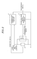
- the illumination light communication device in this embodiment includes, as shown in FIG. 1A , a DC-DC converter 2 connected to a DC power supply 1 as an input source, a rectifier circuit 3 having a diode and a smoothing capacitor C1.
- the DC-DC converter 2 converts a DC voltage from the DC power supply 1 to a predetermined DC voltage by switching it through a switch element Q1 such as a MOSFET and rectifying and smoothing its output through the rectifier circuit 3 and the smoothing capacitor C1.
- a light source unit 4 including light emitting diodes (light emitting elements) LD1 and a current detection resistor 5.
- One end of the current detection resistor 5 is connected to an inverting input terminal of an error amplifier A1. Accordingly, a potential of one end of the current detection resistor 5 is inputted to the inverting input terminal of the error amplifier A1.
- the other end of the current detection resistor 5 is connected to a noninverting input terminal of the error amplifier A1 via a reference voltage source E1.
- the error amplifier A1 outputs, to an output control unit 7, a signal obtained by amplifying a difference between a voltage drop through the current detection resistor 5 and a source voltage of the reference voltage source E1.
- the output control unit 7 controls the on/off of the switch element Q1 based on an externally inputted dimming signal and a feedback signal inputted from the error amplifier A1. Accordingly, the output control unit 7 maintains a load current I1 flowing through the light source unit 4 at a constant value and controls the load current I1 based on the dimming signal.
- phase compensation circuit 6A including a resistor R1 and a capacitor C2 serving as an integral element is connected between the output terminal and the inverting input terminal of the error amplifier A1.
- the phase compensation circuit 6A adjusts a phase of the feedback signal by suppressing the gain in a high frequency region while increasing the gain in a low frequency region.
- a constant current feedback circuit 6 is configured to include the error amplifier A1 and the phase compensation circuit 6A.
- a power supply unit for controlling the load current I1 flowing through the light source unit 4 is configured to include the DC power supply 1, the DC-DC converter 2, the rectifier circuit 3, the smoothing capacitor C1, the current detection resistor 5, the constant current feedback circuit 6 and the output control unit 7.
- the impedance unit Z1 includes, e.g., a plurality of impedance elements (not shown) such as variable resistors and is configured so as to change the impedance by an externally inputted selection signal.
- the impedance unit Z1 includes a series circuit or parallel circuit of each impedance element Zi and one or more switching elements SWi, or a combination thereof. Further, the impedance unit Z1 can vary the impedance by controlling the on/off of each switching element appropriately based on the selection signal.
- the impedance unit Z1 can be connected to or disconnected from the light source unit 4.
- the magnitude of the load current I1 flowing through the light source unit 4 i.e., the light intensity of the illumination light from the light source unit 4. Consequently, it is possible to modulate the light intensity of the illumination light from the light source unit 4.
- the impedance of the impedance unit Z1 since it is possible to change the impedance of the impedance unit Z1 based on the selection signal, it is possible to finely adjust the magnitude of the load current I1 flowing through the light source unit 4, i.e., the modulation width of the light intensity of the illumination light from the light source unit 4.
- a dimming rate detection circuit 8 for detecting a dimming rate of the light source unit 4 and a communication signal generating circuit 9 for generating a communication signal.
- the dimming rate detection circuit 8 detects the dimming rate of the light source unit 4 based on the load current or the load voltage of the light source unit 4, generates a selection signal based on the detected dimming rate and outputs the selection signal to the impedance unit Z1. That is, the dimming rate detection circuit 8 variably controls the impedance of the impedance unit Z1 based on the detected dimming rate.
- the communication signal generating circuit 9 generates a binary communication signal and outputs the binary communication signal to the switch element Q2.
- the communication signal generating circuit 9 generates the binary communication signal on the basis of a transmission signal inputted from an external device (not shown). That is, in this embodiment, a control unit is configured to include the dimming rate detection circuit 8 and the communication signal generating circuit 9 to control the on/off of the switch element Q2 such that the communication signal is superimposed on the illumination light outputted from the light source unit 4.
- the visible light communication is carried out by modulating the light intensity of the illumination light from the light source unit 4 by using the communication signal, and a four pulse position modulation (4PPM) scheme is employed as its modulation scheme.
- the four pulse position modulation is to transmit two bits of data by dividing a predetermined time defined as a symbol time into four slots, and inputting a pulse to any one of these slots, as shown in FIG. 3 .
- the communication signal (4PPM signal) in one symbol time is "1000”
- data of "00” can be transmitted
- the communication signal in one symbol time is "0100”
- data of "01” can be transmitted.
- the communication signal in one symbol time is "0010”
- data of "10” can be transmitted
- the communication signal in one symbol time is "0001”
- data of "11” can be transmitted.
- the light emission time having a large light intensity per symbol time is 25%, and the illumination efficiency becomes poor.
- the light intensity of the illumination light from the light source unit 4 is reduced when the pulse of the communication signal is superimposed on the illumination light and is increased when the pulse of the communication signal is not superimposed on the illumination light has been employed. Accordingly, the light emission time having a large light intensity per symbol time is ensured to be at least 75%, thereby improving the illumination efficiency.
- the impedance of the impedance unit Z1 is controlled such that a difference between the magnitude of the load current I1 when the pulse of the communication signal is superimposed and the magnitude of the load current I1 when the pulse of the communication signal is not superimposed is kept constant regardless of the dimming rate in a range of a dimming rate equal to or greater than a predetermined dimming rate. Further, the impedance of the impedance unit Z1 is controlled such that the light source unit 4 is turned off when the pulse of the communication signal is superimposed in a range of a dimming rate less than the predetermined dimming rate.
- the impedance of the impedance unit Z1 when the switch element Q2 is turned off is controlled such that a difference between the magnitude of the load current I1 when the pulse of the communication signal is superimposed and the magnitude of the load current I1 when the pulse of the communication signal is not superimposed becomes constant, i.e., an amplitude depth D1, regardless of the dimming rate, wherein the amplitude depth D1 is a difference between a maximum and a minimum of the load current I1 when the dimming rate is 100%.
- the dimming rate is less than 50%
- the impedance of the impedance unit Z1 is controlled such that the magnitude of the load current I1 when the pulse of the communication signal is superimposed becomes zero.
- the amplitude depth D1 can be maintained at a constant until the dimming rate becomes 50%.
- a dimming rate ratio e.g., dimming rate of 50%/ dimming rate of 100%
- a load current ratio e.g., magnitude of the load current at the dimming rate of 50%/magnitude of the load current at the dimming rate of 100%
- the difference between the maximum and the minimum of the light intensity of the illumination light from the light source unit 4 can be sufficiently large even if the dimming is controlled to result in a low light level, and thus it is easier to detect the difference on the receiver side, and fine communication can be maintained.
- the amplitude depth D1 cannot be maintained at a constant, however, as shown in FIG. 1B , two values of the binary communication signal correspond to the presence/absence of the load current I1, i.e., the turn-on/turn-off of the light source unit 4. For this reason, the communication signal can be easily detected on the receiver side based on the presence/absence of the light intensity, so that it is possible to maintain fine communication.
- the modulation degree can be defined as follow:
- the modulation degree is set to 50% and the dimming rate of 50% is set as a boundary condition in the above embodiment, they are merely exemplary values, and the modulation degree and the dimming rate set as a boundary condition can be changed variously. However, the dimming rate set as a boundary condition is required to be greater than zero.
- the impedance of the impedance unit Z1 is controlled such that the modulation degree of the light intensity of the illumination light from the light source unit 4 is kept constant in a range of a dimming rate equal to or greater than a predetermined dimming rate, while an amplitude depth D2 of the light intensity of the illumination light from the light source unit 4 is kept constant in a range of a dimming rate less than the predetermined dimming rate.
- the impedance of the impedance unit Z1 is controlled such that the modulation degree is maintained at 50% irrespective of changes in the dimming rate.
- the dimming result is controlled to be not too dark, even if it is controlled to make the modulation degree constant as in the conventional case, the difference between the maximum and the minimum of the light intensity of the illumination light from the light source unit 4 can be sufficiently large. Accordingly, it is easier to detect such difference on the receiver side, and fine communication can be maintained.
- the impedance of the impedance unit Z1 is controlled such that the amplitude depth D2 at the modulation degree of 50% in case where the dimming rate is 40% is maintained constant regardless of the dimming rate.
- the impedance of the impedance unit Z1 is controlled such that the difference between the magnitudes of the load currents I1 flowing through the light source unit 4 respectively when the pulse of the communication signal is superimposed and when the pulse of the communication signal is not superimposed is kept constant regardless of the dimming rate.
- the difference between the maximum and the minimum of the light intensity of the illumination light from the light source unit 4 can be sufficiently large even if the dimming is controlled to result in a low light level, and thus it is easier to detect such difference on the receiver side, and fine communication can be maintained.
- the amplitude depth D2 cannot be maintained at a constant.
- two values of the binary communication signal correspond to the presence/absence of the load current I1, i.e., the turn-on/turn-off of the light source unit 4. For this reason, the communication signal can be easily detected on the receiver side based on the presence/absence of the light intensity, so that it is possible to maintain fine communication.
- the modulation degree is set to 50% and the dimming rates of 40% and 20% are set as a boundary condition in the above embodiment, they are merely exemplary values, and the modulation degree and the dimming rate set as a boundary condition can be changed variously. However, the dimming rate set as a boundary condition is required to be greater than zero.
- a switching circuit SW1 is connected in series to the light source unit 4 to open and close a path connecting between the smoothing capacitor C1 and the light source unit 4.
- the switching circuit SW1 is switched on/off on the basis of a switching signal applied from the dimming rate detection circuit 8.
- the light source unit 4 can be dimmed by a so-called PWM control in which a period (ON time) during which the load current I1 flows through the light source unit 4 and a period (OFF time) during which no load current I1 flows through the light source unit 4 are alternately repeated.
- the impedance of the impedance unit Z1 is controlled such that the modulation degree of the light intensity of the illumination light from the light source unit 4 is maintained constant in a range of a dimming rate equal to or greater than a predetermined dimming rate in the same way as in the second embodiment.
- dimming on the light source unit 4 is performed by the PWM control to change a ratio of on-duty per unit time (e.g., 1/9600 second) of the load current I1 flowing through the light source unit 4.
- the impedance of the impedance unit Z1 is controlled such that the modulation degree is maintained at 50% irrespective of changes in the dimming rate.
- the difference between the maximum and the minimum of the light intensity of the illumination light from the light source unit 4 can be sufficiently large. Accordingly, it is easier to detect the difference on the receiver side, and fine communication can be maintained.
- the dimming rate detection circuit 8 starts controlling to switch the on/off of the switching circuit SW1 by providing a switching signal to the switching circuit SW1, thereby starting to perform dimming on the light source unit 4 by the PWM control.
- the impedance of the impedance unit Z1 is controlled such that the difference between the magnitude of the load current I1 when the pulse of the communication signal is superimposed and the magnitude of the load current I1 when the pulse of the communication signal is not superimposed becomes constant, i.e., the amplitude depth D3, regardless of the dimming rate, wherein the amplitude depth D3 is an amplitude depth of the light intensity of the illumination light from the light source unit 4 at the modulation degree of 50% in case where the dimming rate is 20%. Therefore, in this embodiment, the range of the dimming control can be further expanded to a lower light level while the amplitude depth D3 of the load current I1 is maintained constant.
- the dimming rate can be reduced to, e.g., 15%, 10% or 5% by reducing a ratio of on-duty per unit time of the load current I1 as shown in FIG. 5C .
- the dimming rate can be reduced to, e.g., 7.5%, 5% or 2.5% by reducing a ratio of on-duty per unit time of the load current I1 as shown in FIG. 5C .
- dimming can be performed up to the dimming rate of 1% when a ratio of on-duty per unit time of the load current I1 is reduced to 10%.
- a switching frequency of the switching circuit SW1 at the time of the PWM control is equal to the frequency (e.g., 9.6 kHz) of the communication signal to be superimposed, and the PWM control is carried out in synchronization with the communication signal. Further, the switching frequency may be set to an integer multiple of the frequency of communication signal.
- the dimming signal externally inputted to the output control unit 7 is also inputted to the dimming rate detection circuit 8. Accordingly, in a range where the dimming rate is equal to or greater than 20%, the dimming rate detection circuit 8 detects the load current controlled by the output control unit 7 to detect the dimming rate of the light source unit 4, and variably controls the impedance of the impedance unit Z1 based on the detected dimming rate.
- the dimming rate detection circuit 8 detects the dimming rate based on the dimming signal inputted to the dimming rate detection circuit 8 rather than the load current or load voltage. That is, in a range where the dimming rate is less than 20%, when the dimming rate detection circuit 8 detects that the dimming rate becomes less than 20% based on the dimming signal, it transmits a signal to the output control unit 7 to maintain the load current at the dimming rate of 20%, thereby performing the PWM control to control the on/off of the switching circuit SW1 while maintaining the load current at the dimming rate of 20%.
- the dimming rate can be reduced by reducing a ratio of on-duty per unit time of the load current while the impedance of the impedance unit Z1 is controlled such that the difference (amplitude depth D3) between the magnitude of the load current when the pulse of the communication signal is superimposed and the magnitude of the load current when the pulse of the communication signal is not superimposed is kept constant regardless of the dimming rate.
- the dimming rate of 20% is set as a boundary condition in this embodiment
- the dimming rate of 40% may be set as a boundary condition. That is, the modulation degree of 50% and the dimming rate of 20% in the above embodiment are merely exemplary values, and the modulation degree and the dimming rate set as a boundary condition can be changed variously. However, the dimming rate set as a boundary condition is required to be greater than zero.
- the first embodiment and the third embodiment may be combined with each other.
- the impedance of the impedance unit Z1 is controlled such that the amplitude depth D1 of the light intensity of the illumination light from the light source unit 4 is kept constant regardless of the dimming rate.
- the dimming rate may be controlled by the PWM control to control the on/off of the switching circuit SW1 as in the third embodiment while the load current is maintained at the dimming rate of 50% and the amplitude depth D1 of the light intensity of the illumination light from the light source unit 4 when the pulse of the communication signal is superimposed is maintained constant.
- the second embodiment and the third embodiment may be combined with each other.
- the dimming rate is equal to or greater than 40%
- it is controlled such that the modulation degree is maintained constant.
- the dimming rate is equal to or greater than 20% and less than 40%
- it is controlled such that the difference between the magnitudes of the load currents respectively when the pulse of the communication signal is superimposed and when the pulse of the communication signal is not superimposed is maintained constant regardless of the dimming rate.
- the dimming rate may be controlled by the PWM control as in the third embodiment while the load current is maintained at the dimming rate of 20% and the amplitude depth D3 of the light intensity of the illumination light from the light source unit 4 when the pulse of the communication signal is superimposed is maintained constant.
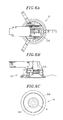
- An illumination apparatus 10 of this embodiment is, e.g., of a down light with a mortar-shaped apparatus body 10A whose bottom is open as shown in FIG. 6A to 6C . Further, the illumination light communication device (not shown) of any of the first to third embodiments is retained in the apparatus body 10A.
- the light source unit 4 included in the illumination light communication device is disposed to face an external space through a bottom opening of the apparatus body 10A, and irradiates illumination light toward the external space.
- the illumination apparatus 10 may be an illumination apparatus having other configurations without being limited to the down light.
- the illumination system in this embodiment includes, as shown in FIG. 7A , the illumination light communication device (not shown) of one of the first to third embodiments and a receiver 11 which receives the communication signal transmitted from the illumination light communication device. Further, in this embodiment, the illumination light communication device is retained in the illumination apparatus 10 embedded in the ceiling.
- the receiver 11 is formed of, e.g., a mobile terminal and includes a photodiode 11A receiving the illumination light irradiated from the illumination apparatus 10, as shown in FIG. 7B . Further, the receiver 11 includes a display unit 11B formed of, e.g., a liquid crystal monitor or the like, an operation unit (not shown), and a processing circuit (not shown) which reads the communication signal based on the light intensity of the illumination light received by the photodiode 11A. Further, the operation unit may be implemented by configuring the display unit 11B as a touch panel. In addition, the receiver 11 may be a receiver having other configurations without being limited to the mobile terminal.
- the user is in possession of the receiver 11 and can receive the communication signal superimposed on the illumination light from the illumination apparatus 10 within an illumination range of the illumination apparatus 10.
- the receiver 11 detects, e.g., position information contained in the communication signal and displays an image on the display unit 11B or outputs voice through a built-in speaker, thereby informing the user of a current position.
- the purpose of this embodiment may be any other purpose without being limited to the purpose of informing the user of the current position.
- the visible light communication is performed by using the illumination light communication device of one of the first to third embodiments, fine communication can be maintained even if the dimming is controlled to result in a low light level.
- the light emitting diodes LD1 are used as light emitting elements included in the light source unit 4.
- other light emitting elements such as organic electroluminescence (EL) elements and semiconductor lasers may be used.
Landscapes
- Engineering & Computer Science (AREA)
- Computer Networks & Wireless Communication (AREA)
- Physics & Mathematics (AREA)
- Electromagnetism (AREA)
- Signal Processing (AREA)
- Circuit Arrangement For Electric Light Sources In General (AREA)
- Optical Communication System (AREA)
Applications Claiming Priority (1)
| Application Number | Priority Date | Filing Date | Title |
|---|---|---|---|
| JP2011157173A JP5906408B2 (ja) | 2011-07-15 | 2011-07-15 | 照明光通信装置及びそれを用いた照明器具、並びに照明システム |
Publications (3)
| Publication Number | Publication Date |
|---|---|
| EP2547174A2 true EP2547174A2 (fr) | 2013-01-16 |
| EP2547174A3 EP2547174A3 (fr) | 2014-10-22 |
| EP2547174B1 EP2547174B1 (fr) | 2017-01-11 |
Family
ID=47010180
Family Applications (1)
| Application Number | Title | Priority Date | Filing Date |
|---|---|---|---|
| EP12176282.7A Active EP2547174B1 (fr) | 2011-07-15 | 2012-07-13 | Appareil de éclairage et communication, et système |
Country Status (4)
| Country | Link |
|---|---|
| US (1) | US8810155B2 (fr) |
| EP (1) | EP2547174B1 (fr) |
| JP (1) | JP5906408B2 (fr) |
| CN (1) | CN102882599B (fr) |
Cited By (7)
| Publication number | Priority date | Publication date | Assignee | Title |
|---|---|---|---|---|
| EP2744124A1 (fr) * | 2012-12-11 | 2014-06-18 | Panasonic Corporation | Dispositif de communication de lumière d'éclairage |
| WO2014149596A3 (fr) * | 2013-03-15 | 2014-11-13 | Microchip Technology Incorporated | Port de communications d'attaque de del à luminosité constante |
| FR3019268A1 (fr) * | 2014-03-26 | 2015-10-02 | Luciom | Dispositif de commande de l'intensite lumineuse d'ambiance d'un systeme d'eclairage et de transfert de donnees |
| WO2016074961A1 (fr) * | 2014-11-11 | 2016-05-19 | Philips Lighting Holding B.V. | Commande d'élément d'éclairage |
| WO2017140436A1 (fr) * | 2016-02-18 | 2017-08-24 | Osram Gmbh | Dispositif et procédé de communication pour la communication à base de rayonnement entre des véhicules et véhicule équipé dudit dispositif de communication |
| WO2018073069A1 (fr) | 2016-10-21 | 2018-04-26 | Philips Lighting Holding B.V. | Circuit de modulation de courant, circuit d'attaque et procédé de commande d'une charge d'éclairage avec modulation de courant |
| EP3945750A1 (fr) * | 2020-07-29 | 2022-02-02 | Eaton Intelligent Power Limited | Luminaire et système d'éclairage |
Families Citing this family (34)
| Publication number | Priority date | Publication date | Assignee | Title |
|---|---|---|---|---|
| US9455783B2 (en) * | 2013-05-06 | 2016-09-27 | Federal Law Enforcement Development Services, Inc. | Network security and variable pulse wave form with continuous communication |
| WO2008148053A1 (fr) | 2007-05-24 | 2008-12-04 | Federal Law Enforcement Development Services, Inc. | Système mondial de localisation (gps) et de communication d'acheminement à éclairage à del |
| US9100124B2 (en) | 2007-05-24 | 2015-08-04 | Federal Law Enforcement Development Services, Inc. | LED Light Fixture |
| US9414458B2 (en) | 2007-05-24 | 2016-08-09 | Federal Law Enforcement Development Services, Inc. | LED light control assembly and system |
| US11265082B2 (en) | 2007-05-24 | 2022-03-01 | Federal Law Enforcement Development Services, Inc. | LED light control assembly and system |
| US8890773B1 (en) | 2009-04-01 | 2014-11-18 | Federal Law Enforcement Development Services, Inc. | Visible light transceiver glasses |
| US8767902B2 (en) * | 2010-02-22 | 2014-07-01 | Advanced Reactor Concepts LLC | Small, fast neutron spectrum nuclear power plant with a long refueling interval |
| JP5842161B2 (ja) * | 2011-11-22 | 2016-01-13 | パナソニックIpマネジメント株式会社 | 照明器具及び同器具を用いた可視光通信システム |
| KR101432250B1 (ko) * | 2012-11-26 | 2014-09-25 | 경희대학교 산학협력단 | 가시광 통신 시스템과, 그 시스템에서의 데이터 변조 방법 및 성능 정보 궤환 방법 |
| CN203519822U (zh) * | 2013-04-09 | 2014-04-02 | 北京半导体照明科技促进中心 | 基于可见光的室内定位装置和系统 |
| US9407367B2 (en) | 2013-04-25 | 2016-08-02 | Beijing Guo Cheng Wan Tong Information Co. Ltd | Methods and devices for transmitting/obtaining information by visible light signals |
| JP6145928B2 (ja) * | 2013-04-25 | 2017-06-14 | パナソニックIpマネジメント株式会社 | 可視光通信装置およびそれを用いた照明器具 |
| JP6120217B2 (ja) * | 2013-04-26 | 2017-04-26 | パナソニックIpマネジメント株式会社 | 可視光通信装置およびそれを用いた照明器具 |
| CN103259186A (zh) * | 2013-04-27 | 2013-08-21 | 南京理工大学 | 基于pwm控制的半导体激光器电源装置 |
| JP6264821B2 (ja) * | 2013-10-07 | 2018-01-24 | パナソニックIpマネジメント株式会社 | 可視光通信装置 |
| US20150198941A1 (en) | 2014-01-15 | 2015-07-16 | John C. Pederson | Cyber Life Electronic Networking and Commerce Operating Exchange |
| US9432116B2 (en) | 2014-10-07 | 2016-08-30 | Abl Ip Holding Llc | Use of very high frequency switching power converters for also modulating light output from solid state emitter to communicate data |
| CN104539361B (zh) * | 2015-01-04 | 2017-06-30 | 中国联合网络通信集团有限公司 | 一种室内可见光通信中调节光照范围的方法和照明装置 |
| JP6504447B2 (ja) | 2015-04-03 | 2019-04-24 | パナソニックIpマネジメント株式会社 | 点灯装置、照明装置および看板装置 |
| US20170048953A1 (en) | 2015-08-11 | 2017-02-16 | Federal Law Enforcement Development Services, Inc. | Programmable switch and system |
| CN107925440B (zh) * | 2015-08-12 | 2021-09-21 | 费斯托股份两合公司 | 现场设备耦合单元和系统 |
| JP6631913B2 (ja) * | 2016-01-21 | 2020-01-15 | パナソニックIpマネジメント株式会社 | 照明器具 |
| JP6607522B2 (ja) * | 2016-03-24 | 2019-11-20 | 東芝ライテック株式会社 | 点灯装置および照明器具 |
| TWI655446B (zh) * | 2016-04-08 | 2019-04-01 | 財團法人工業技術研究院 | 可見光定位系統與定位方法 |
| US9954614B2 (en) | 2016-04-08 | 2018-04-24 | Industrial Technology Research Institute | Luminaire positioning system and method thereof |
| JP6771182B2 (ja) * | 2016-04-27 | 2020-10-21 | パナソニックIpマネジメント株式会社 | 信号送信装置、信号受信装置、点灯システム、照明器具、及び照明システム |
| TWI600286B (zh) | 2016-08-09 | 2017-09-21 | 財團法人工業技術研究院 | 可見光通訊裝置與其驅動方法 |
| JP6799819B2 (ja) | 2017-01-30 | 2020-12-16 | パナソニックIpマネジメント株式会社 | 点灯装置、照明器具及び看板 |
| JP6837218B2 (ja) | 2017-01-30 | 2021-03-03 | パナソニックIpマネジメント株式会社 | 点灯装置、照明器具及び看板 |
| JP6899549B2 (ja) * | 2017-05-25 | 2021-07-07 | パナソニックIpマネジメント株式会社 | 点灯装置、照明器具、及び、看板 |
| JP6979588B2 (ja) * | 2018-02-23 | 2021-12-15 | パナソニックIpマネジメント株式会社 | 照明光通信装置 |
| CN109148402B (zh) * | 2018-08-29 | 2020-09-15 | 开发晶照明(厦门)有限公司 | 发光二极管封装结构及其制造方法 |
| US12022587B2 (en) | 2020-02-25 | 2024-06-25 | Signify Holding B.V. | LED lighting system and control method |
| CN112291885B (zh) * | 2020-12-29 | 2021-03-09 | 南京优利博电气科技有限公司 | 一种智慧照明功耗控制系统 |
Citations (1)
| Publication number | Priority date | Publication date | Assignee | Title |
|---|---|---|---|---|
| JP2011034713A (ja) | 2009-07-30 | 2011-02-17 | Toshiba Lighting & Technology Corp | 照明器具 |
Family Cites Families (18)
| Publication number | Priority date | Publication date | Assignee | Title |
|---|---|---|---|---|
| JP3981036B2 (ja) * | 2003-03-27 | 2007-09-26 | 株式会社東芝 | ワイヤレス光通信システム |
| JP4333186B2 (ja) * | 2003-04-07 | 2009-09-16 | ソニー株式会社 | 通信システム及び通信照明装置 |
| JP4641767B2 (ja) * | 2004-09-01 | 2011-03-02 | アバゴ・テクノロジーズ・イーシービーユー・アイピー(シンガポール)プライベート・リミテッド | 光通信システム及びそれに用いられる照明装置 |
| JP4692991B2 (ja) * | 2005-05-20 | 2011-06-01 | 株式会社中川研究所 | データ送信装置及びデータ受信装置 |
| JP4325604B2 (ja) * | 2005-09-30 | 2009-09-02 | 日本電気株式会社 | 可視光制御装置、可視光通信装置、可視光制御方法及びプログラム |
| US7656103B2 (en) * | 2006-01-20 | 2010-02-02 | Exclara, Inc. | Impedance matching circuit for current regulation of solid state lighting |
| JP5000327B2 (ja) * | 2007-02-22 | 2012-08-15 | パナソニック株式会社 | 可視光通信システム |
| JP4577525B2 (ja) * | 2007-05-31 | 2010-11-10 | 東芝ライテック株式会社 | 照明装置 |
| JP2009117892A (ja) * | 2007-11-01 | 2009-05-28 | Toshiba Corp | 可視光通信装置 |
| TW200949325A (en) * | 2008-02-12 | 2009-12-01 | Koninkl Philips Electronics Nv | Adaptive modulation and data embedding in light for advanced lighting control |
| JP4687735B2 (ja) * | 2008-03-24 | 2011-05-25 | 東芝ライテック株式会社 | 電源装置及び照明器具 |
| JP4573885B2 (ja) * | 2008-06-26 | 2010-11-04 | シャープ株式会社 | 照明光受信装置及び照明光通信システム |
| JP4600583B2 (ja) * | 2008-09-10 | 2010-12-15 | 東芝ライテック株式会社 | 調光機能を有する電源装置及び照明器具 |
| JP2010193365A (ja) * | 2009-02-20 | 2010-09-02 | Toshiba Lighting & Technology Corp | 可視光通信システム |
| CN101938310A (zh) * | 2010-07-21 | 2011-01-05 | 中国科学院半导体研究所 | 一种可见光通信控制系统及其实现方法 |
| US8729811B2 (en) * | 2010-07-30 | 2014-05-20 | Cirrus Logic, Inc. | Dimming multiple lighting devices by alternating energy transfer from a magnetic storage element |
| TWI424782B (zh) * | 2010-11-12 | 2014-01-21 | Au Optronics Corp | 光源系統與發光二極體驅動方法 |
| JP5891393B2 (ja) * | 2011-07-15 | 2016-03-23 | パナソニックIpマネジメント株式会社 | 照明光通信装置及びそれを用いた照明器具、並びに照明システム |
-
2011
- 2011-07-15 JP JP2011157173A patent/JP5906408B2/ja active Active
-
2012
- 2012-07-12 US US13/547,361 patent/US8810155B2/en active Active
- 2012-07-13 EP EP12176282.7A patent/EP2547174B1/fr active Active
- 2012-07-16 CN CN201210246797.4A patent/CN102882599B/zh active Active
Patent Citations (1)
| Publication number | Priority date | Publication date | Assignee | Title |
|---|---|---|---|---|
| JP2011034713A (ja) | 2009-07-30 | 2011-02-17 | Toshiba Lighting & Technology Corp | 照明器具 |
Cited By (13)
| Publication number | Priority date | Publication date | Assignee | Title |
|---|---|---|---|---|
| US9385806B2 (en) | 2012-12-11 | 2016-07-05 | Panasonic Intellectual Property Management Co., Ltd. | Visible light communication device |
| EP2744124A1 (fr) * | 2012-12-11 | 2014-06-18 | Panasonic Corporation | Dispositif de communication de lumière d'éclairage |
| WO2014149596A3 (fr) * | 2013-03-15 | 2014-11-13 | Microchip Technology Incorporated | Port de communications d'attaque de del à luminosité constante |
| US9210769B2 (en) | 2013-03-15 | 2015-12-08 | Microchip Technology Incorporated | Constant brightness LED drive communications port |
| EP2974538B1 (fr) * | 2013-03-15 | 2024-05-22 | Microchip Technology Incorporated | Port de communications d'attaque de del à luminosité constante |
| FR3019268A1 (fr) * | 2014-03-26 | 2015-10-02 | Luciom | Dispositif de commande de l'intensite lumineuse d'ambiance d'un systeme d'eclairage et de transfert de donnees |
| US10820389B2 (en) | 2014-11-11 | 2020-10-27 | Signify Holding B.V. | Driving a lighting element |
| WO2016074961A1 (fr) * | 2014-11-11 | 2016-05-19 | Philips Lighting Holding B.V. | Commande d'élément d'éclairage |
| RU2707876C2 (ru) * | 2014-11-11 | 2019-12-02 | Филипс Лайтинг Холдинг Б.В. | Возбуждение осветительного элемента |
| WO2017140436A1 (fr) * | 2016-02-18 | 2017-08-24 | Osram Gmbh | Dispositif et procédé de communication pour la communication à base de rayonnement entre des véhicules et véhicule équipé dudit dispositif de communication |
| US10602575B2 (en) | 2016-10-21 | 2020-03-24 | Signify Holding B.V. | Current modulation circuit, a driving circuit, and a method for driving a lighting load with current modulation |
| WO2018073069A1 (fr) | 2016-10-21 | 2018-04-26 | Philips Lighting Holding B.V. | Circuit de modulation de courant, circuit d'attaque et procédé de commande d'une charge d'éclairage avec modulation de courant |
| EP3945750A1 (fr) * | 2020-07-29 | 2022-02-02 | Eaton Intelligent Power Limited | Luminaire et système d'éclairage |
Also Published As
| Publication number | Publication date |
|---|---|
| US20130015785A1 (en) | 2013-01-17 |
| CN102882599A (zh) | 2013-01-16 |
| EP2547174B1 (fr) | 2017-01-11 |
| JP2013026690A (ja) | 2013-02-04 |
| US8810155B2 (en) | 2014-08-19 |
| CN102882599B (zh) | 2015-08-26 |
| JP5906408B2 (ja) | 2016-04-20 |
| EP2547174A3 (fr) | 2014-10-22 |
Similar Documents
| Publication | Publication Date | Title |
|---|---|---|
| EP2547174B1 (fr) | Appareil de éclairage et communication, et système | |
| EP2547173B1 (fr) | Appareil de éclairage et communication, et lampe et système | |
| US8217584B2 (en) | Driving circuit for driving light emitting diodes and dimmer | |
| US20130221875A1 (en) | Light emitting device driver circuit and control method thereof | |
| JP2009123681A (ja) | Led調光装置 | |
| JP5834239B2 (ja) | 照明光通信装置及びそれを用いた照明器具、並びに照明システム | |
| JP5000327B2 (ja) | 可視光通信システム | |
| US10588193B2 (en) | LED module and lighting apparatus | |
| JP2008146949A (ja) | バックライト駆動装置 | |
| EP3531585B1 (fr) | Appareil de communication lumineuse visible | |
| JP2013233033A (ja) | バックライト用ledストリングの駆動回路および駆動方法、ならびにそれを用いたバックライト装置および電子機器 | |
| US9222657B2 (en) | Vehicle lighting device | |
| KR20180017076A (ko) | 스위칭 컨버터 및 그 제어 회로, 그것을 사용한 조명 장치, 전자 기기 | |
| JP2014007078A (ja) | Led駆動回路、led駆動方法、led照明装置、led表示装置、及び、テレビジョン受像機 | |
| US9814113B2 (en) | Voltage converter for operating lamps | |
| JP2014086689A (ja) | 発光装置の制御回路、それを用いた発光装置および電子機器 | |
| US10630052B2 (en) | Efficiency improved driver for laser diode in optical communication | |
| CN111819742B (zh) | 光学通信中效率改善的激光二极管驱动器 | |
| EP4185073B1 (fr) | Système de commande et procédé de commande d'une source de courant d'un dispositif de fonctionnement pour moyens d'éclairage, dispositif d'éclairage et luminaire | |
| US20140062428A1 (en) | Feedback detection circuit | |
| JP6015109B2 (ja) | 点灯装置、電源装置及び調光方法 | |
| JP2019041298A (ja) | 照明光通信装置および通信モジュール | |
| JP2020027751A (ja) | 点灯装置及びそれを用いた照明器具 | |
| JP2010186827A (ja) | 光源駆動装置および光源駆動方法 |
Legal Events
| Date | Code | Title | Description |
|---|---|---|---|
| PUAI | Public reference made under article 153(3) epc to a published international application that has entered the european phase |
Free format text: ORIGINAL CODE: 0009012 |
|
| AK | Designated contracting states |
Kind code of ref document: A2 Designated state(s): AL AT BE BG CH CY CZ DE DK EE ES FI FR GB GR HR HU IE IS IT LI LT LU LV MC MK MT NL NO PL PT RO RS SE SI SK SM TR |
|
| AX | Request for extension of the european patent |
Extension state: BA ME |
|
| 17P | Request for examination filed |
Effective date: 20140327 |
|
| RBV | Designated contracting states (corrected) |
Designated state(s): AL AT BE BG CH CY CZ DE DK EE ES FI FR GB GR HR HU IE IS IT LI LT LU LV MC MK MT NL NO PL PT RO RS SE SI SK SM TR |
|
| PUAL | Search report despatched |
Free format text: ORIGINAL CODE: 0009013 |
|
| AK | Designated contracting states |
Kind code of ref document: A3 Designated state(s): AL AT BE BG CH CY CZ DE DK EE ES FI FR GB GR HR HU IE IS IT LI LT LU LV MC MK MT NL NO PL PT RO RS SE SI SK SM TR |
|
| AX | Request for extension of the european patent |
Extension state: BA ME |
|
| RIC1 | Information provided on ipc code assigned before grant |
Ipc: H04B 10/116 20130101ALI20140912BHEP Ipc: H05B 37/02 20060101ALI20140912BHEP Ipc: H05B 33/08 20060101AFI20140912BHEP |
|
| RAP1 | Party data changed (applicant data changed or rights of an application transferred) |
Owner name: PANASONIC INTELLECTUAL PROPERTY MANAGEMENT CO., LT |
|
| GRAP | Despatch of communication of intention to grant a patent |
Free format text: ORIGINAL CODE: EPIDOSNIGR1 |
|
| INTG | Intention to grant announced |
Effective date: 20160818 |
|
| GRAS | Grant fee paid |
Free format text: ORIGINAL CODE: EPIDOSNIGR3 |
|
| GRAA | (expected) grant |
Free format text: ORIGINAL CODE: 0009210 |
|
| AK | Designated contracting states |
Kind code of ref document: B1 Designated state(s): AL AT BE BG CH CY CZ DE DK EE ES FI FR GB GR HR HU IE IS IT LI LT LU LV MC MK MT NL NO PL PT RO RS SE SI SK SM TR |
|
| REG | Reference to a national code |
Ref country code: GB Ref legal event code: FG4D |
|
| REG | Reference to a national code |
Ref country code: CH Ref legal event code: EP |
|
| REG | Reference to a national code |
Ref country code: AT Ref legal event code: REF Ref document number: 862316 Country of ref document: AT Kind code of ref document: T Effective date: 20170115 |
|
| REG | Reference to a national code |
Ref country code: IE Ref legal event code: FG4D |
|
| REG | Reference to a national code |
Ref country code: DE Ref legal event code: R096 Ref document number: 602012027644 Country of ref document: DE |
|
| REG | Reference to a national code |
Ref country code: LT Ref legal event code: MG4D |
|
| REG | Reference to a national code |
Ref country code: NL Ref legal event code: MP Effective date: 20170111 |
|
| REG | Reference to a national code |
Ref country code: AT Ref legal event code: MK05 Ref document number: 862316 Country of ref document: AT Kind code of ref document: T Effective date: 20170111 |
|
| PG25 | Lapsed in a contracting state [announced via postgrant information from national office to epo] |
Ref country code: NL Free format text: LAPSE BECAUSE OF FAILURE TO SUBMIT A TRANSLATION OF THE DESCRIPTION OR TO PAY THE FEE WITHIN THE PRESCRIBED TIME-LIMIT Effective date: 20170111 |
|
| PG25 | Lapsed in a contracting state [announced via postgrant information from national office to epo] |
Ref country code: FI Free format text: LAPSE BECAUSE OF FAILURE TO SUBMIT A TRANSLATION OF THE DESCRIPTION OR TO PAY THE FEE WITHIN THE PRESCRIBED TIME-LIMIT Effective date: 20170111 Ref country code: LT Free format text: LAPSE BECAUSE OF FAILURE TO SUBMIT A TRANSLATION OF THE DESCRIPTION OR TO PAY THE FEE WITHIN THE PRESCRIBED TIME-LIMIT Effective date: 20170111 Ref country code: IS Free format text: LAPSE BECAUSE OF FAILURE TO SUBMIT A TRANSLATION OF THE DESCRIPTION OR TO PAY THE FEE WITHIN THE PRESCRIBED TIME-LIMIT Effective date: 20170511 Ref country code: HR Free format text: LAPSE BECAUSE OF FAILURE TO SUBMIT A TRANSLATION OF THE DESCRIPTION OR TO PAY THE FEE WITHIN THE PRESCRIBED TIME-LIMIT Effective date: 20170111 Ref country code: NO Free format text: LAPSE BECAUSE OF FAILURE TO SUBMIT A TRANSLATION OF THE DESCRIPTION OR TO PAY THE FEE WITHIN THE PRESCRIBED TIME-LIMIT Effective date: 20170411 Ref country code: GR Free format text: LAPSE BECAUSE OF FAILURE TO SUBMIT A TRANSLATION OF THE DESCRIPTION OR TO PAY THE FEE WITHIN THE PRESCRIBED TIME-LIMIT Effective date: 20170412 |
|
| PG25 | Lapsed in a contracting state [announced via postgrant information from national office to epo] |
Ref country code: PL Free format text: LAPSE BECAUSE OF FAILURE TO SUBMIT A TRANSLATION OF THE DESCRIPTION OR TO PAY THE FEE WITHIN THE PRESCRIBED TIME-LIMIT Effective date: 20170111 Ref country code: ES Free format text: LAPSE BECAUSE OF FAILURE TO SUBMIT A TRANSLATION OF THE DESCRIPTION OR TO PAY THE FEE WITHIN THE PRESCRIBED TIME-LIMIT Effective date: 20170111 Ref country code: BG Free format text: LAPSE BECAUSE OF FAILURE TO SUBMIT A TRANSLATION OF THE DESCRIPTION OR TO PAY THE FEE WITHIN THE PRESCRIBED TIME-LIMIT Effective date: 20170411 Ref country code: AT Free format text: LAPSE BECAUSE OF FAILURE TO SUBMIT A TRANSLATION OF THE DESCRIPTION OR TO PAY THE FEE WITHIN THE PRESCRIBED TIME-LIMIT Effective date: 20170111 Ref country code: RS Free format text: LAPSE BECAUSE OF FAILURE TO SUBMIT A TRANSLATION OF THE DESCRIPTION OR TO PAY THE FEE WITHIN THE PRESCRIBED TIME-LIMIT Effective date: 20170111 Ref country code: SE Free format text: LAPSE BECAUSE OF FAILURE TO SUBMIT A TRANSLATION OF THE DESCRIPTION OR TO PAY THE FEE WITHIN THE PRESCRIBED TIME-LIMIT Effective date: 20170111 Ref country code: LV Free format text: LAPSE BECAUSE OF FAILURE TO SUBMIT A TRANSLATION OF THE DESCRIPTION OR TO PAY THE FEE WITHIN THE PRESCRIBED TIME-LIMIT Effective date: 20170111 Ref country code: PT Free format text: LAPSE BECAUSE OF FAILURE TO SUBMIT A TRANSLATION OF THE DESCRIPTION OR TO PAY THE FEE WITHIN THE PRESCRIBED TIME-LIMIT Effective date: 20170511 |
|
| REG | Reference to a national code |
Ref country code: DE Ref legal event code: R097 Ref document number: 602012027644 Country of ref document: DE |
|
| PG25 | Lapsed in a contracting state [announced via postgrant information from national office to epo] |
Ref country code: CZ Free format text: LAPSE BECAUSE OF FAILURE TO SUBMIT A TRANSLATION OF THE DESCRIPTION OR TO PAY THE FEE WITHIN THE PRESCRIBED TIME-LIMIT Effective date: 20170111 Ref country code: SK Free format text: LAPSE BECAUSE OF FAILURE TO SUBMIT A TRANSLATION OF THE DESCRIPTION OR TO PAY THE FEE WITHIN THE PRESCRIBED TIME-LIMIT Effective date: 20170111 Ref country code: RO Free format text: LAPSE BECAUSE OF FAILURE TO SUBMIT A TRANSLATION OF THE DESCRIPTION OR TO PAY THE FEE WITHIN THE PRESCRIBED TIME-LIMIT Effective date: 20170111 Ref country code: EE Free format text: LAPSE BECAUSE OF FAILURE TO SUBMIT A TRANSLATION OF THE DESCRIPTION OR TO PAY THE FEE WITHIN THE PRESCRIBED TIME-LIMIT Effective date: 20170111 Ref country code: IT Free format text: LAPSE BECAUSE OF FAILURE TO SUBMIT A TRANSLATION OF THE DESCRIPTION OR TO PAY THE FEE WITHIN THE PRESCRIBED TIME-LIMIT Effective date: 20170111 |
|
| PLBE | No opposition filed within time limit |
Free format text: ORIGINAL CODE: 0009261 |
|
| STAA | Information on the status of an ep patent application or granted ep patent |
Free format text: STATUS: NO OPPOSITION FILED WITHIN TIME LIMIT |
|
| PG25 | Lapsed in a contracting state [announced via postgrant information from national office to epo] |
Ref country code: SM Free format text: LAPSE BECAUSE OF FAILURE TO SUBMIT A TRANSLATION OF THE DESCRIPTION OR TO PAY THE FEE WITHIN THE PRESCRIBED TIME-LIMIT Effective date: 20170111 Ref country code: DK Free format text: LAPSE BECAUSE OF FAILURE TO SUBMIT A TRANSLATION OF THE DESCRIPTION OR TO PAY THE FEE WITHIN THE PRESCRIBED TIME-LIMIT Effective date: 20170111 |
|
| 26N | No opposition filed |
Effective date: 20171012 |
|
| PG25 | Lapsed in a contracting state [announced via postgrant information from national office to epo] |
Ref country code: SI Free format text: LAPSE BECAUSE OF FAILURE TO SUBMIT A TRANSLATION OF THE DESCRIPTION OR TO PAY THE FEE WITHIN THE PRESCRIBED TIME-LIMIT Effective date: 20170111 |
|
| REG | Reference to a national code |
Ref country code: CH Ref legal event code: PL |
|
| GBPC | Gb: european patent ceased through non-payment of renewal fee |
Effective date: 20170713 |
|
| REG | Reference to a national code |
Ref country code: IE Ref legal event code: MM4A |
|
| REG | Reference to a national code |
Ref country code: FR Ref legal event code: ST Effective date: 20180330 |
|
| PG25 | Lapsed in a contracting state [announced via postgrant information from national office to epo] |
Ref country code: CH Free format text: LAPSE BECAUSE OF NON-PAYMENT OF DUE FEES Effective date: 20170731 Ref country code: LI Free format text: LAPSE BECAUSE OF NON-PAYMENT OF DUE FEES Effective date: 20170731 Ref country code: GB Free format text: LAPSE BECAUSE OF NON-PAYMENT OF DUE FEES Effective date: 20170713 Ref country code: IE Free format text: LAPSE BECAUSE OF NON-PAYMENT OF DUE FEES Effective date: 20170713 |
|
| PG25 | Lapsed in a contracting state [announced via postgrant information from national office to epo] |
Ref country code: FR Free format text: LAPSE BECAUSE OF NON-PAYMENT OF DUE FEES Effective date: 20170731 |
|
| REG | Reference to a national code |
Ref country code: BE Ref legal event code: MM Effective date: 20170731 |
|
| PG25 | Lapsed in a contracting state [announced via postgrant information from national office to epo] |
Ref country code: LU Free format text: LAPSE BECAUSE OF NON-PAYMENT OF DUE FEES Effective date: 20170713 |
|
| PG25 | Lapsed in a contracting state [announced via postgrant information from national office to epo] |
Ref country code: BE Free format text: LAPSE BECAUSE OF NON-PAYMENT OF DUE FEES Effective date: 20170731 |
|
| PG25 | Lapsed in a contracting state [announced via postgrant information from national office to epo] |
Ref country code: MT Free format text: LAPSE BECAUSE OF NON-PAYMENT OF DUE FEES Effective date: 20170713 |
|
| PG25 | Lapsed in a contracting state [announced via postgrant information from national office to epo] |
Ref country code: HU Free format text: LAPSE BECAUSE OF FAILURE TO SUBMIT A TRANSLATION OF THE DESCRIPTION OR TO PAY THE FEE WITHIN THE PRESCRIBED TIME-LIMIT; INVALID AB INITIO Effective date: 20120713 Ref country code: MC Free format text: LAPSE BECAUSE OF FAILURE TO SUBMIT A TRANSLATION OF THE DESCRIPTION OR TO PAY THE FEE WITHIN THE PRESCRIBED TIME-LIMIT Effective date: 20170111 |
|
| PG25 | Lapsed in a contracting state [announced via postgrant information from national office to epo] |
Ref country code: CY Free format text: LAPSE BECAUSE OF NON-PAYMENT OF DUE FEES Effective date: 20170111 |
|
| REG | Reference to a national code |
Ref country code: DE Ref legal event code: R079 Ref document number: 602012027644 Country of ref document: DE Free format text: PREVIOUS MAIN CLASS: H05B0033080000 Ipc: H05B0045000000 |
|
| PG25 | Lapsed in a contracting state [announced via postgrant information from national office to epo] |
Ref country code: MK Free format text: LAPSE BECAUSE OF FAILURE TO SUBMIT A TRANSLATION OF THE DESCRIPTION OR TO PAY THE FEE WITHIN THE PRESCRIBED TIME-LIMIT Effective date: 20170111 |
|
| PG25 | Lapsed in a contracting state [announced via postgrant information from national office to epo] |
Ref country code: TR Free format text: LAPSE BECAUSE OF FAILURE TO SUBMIT A TRANSLATION OF THE DESCRIPTION OR TO PAY THE FEE WITHIN THE PRESCRIBED TIME-LIMIT Effective date: 20170111 |
|
| PG25 | Lapsed in a contracting state [announced via postgrant information from national office to epo] |
Ref country code: AL Free format text: LAPSE BECAUSE OF FAILURE TO SUBMIT A TRANSLATION OF THE DESCRIPTION OR TO PAY THE FEE WITHIN THE PRESCRIBED TIME-LIMIT Effective date: 20170111 |
|
| PGFP | Annual fee paid to national office [announced via postgrant information from national office to epo] |
Ref country code: DE Payment date: 20230719 Year of fee payment: 12 |