EP2546731A2 - Positionserkennungssensor und Positionsdetektor - Google Patents
Positionserkennungssensor und Positionsdetektor Download PDFInfo
- Publication number
- EP2546731A2 EP2546731A2 EP12169444A EP12169444A EP2546731A2 EP 2546731 A2 EP2546731 A2 EP 2546731A2 EP 12169444 A EP12169444 A EP 12169444A EP 12169444 A EP12169444 A EP 12169444A EP 2546731 A2 EP2546731 A2 EP 2546731A2
- Authority
- EP
- European Patent Office
- Prior art keywords
- detecting sensor
- position detecting
- axis direction
- disposed
- plural
- Prior art date
- Legal status (The legal status is an assumption and is not a legal conclusion. Google has not performed a legal analysis and makes no representation as to the accuracy of the status listed.)
- Withdrawn
Links
Images





Classifications
-
- G—PHYSICS
- G06—COMPUTING OR CALCULATING; COUNTING
- G06F—ELECTRIC DIGITAL DATA PROCESSING
- G06F3/00—Input arrangements for transferring data to be processed into a form capable of being handled by the computer; Output arrangements for transferring data from processing unit to output unit, e.g. interface arrangements
- G06F3/01—Input arrangements or combined input and output arrangements for interaction between user and computer
- G06F3/03—Arrangements for converting the position or the displacement of a member into a coded form
- G06F3/041—Digitisers, e.g. for touch screens or touch pads, characterised by the transducing means
- G06F3/046—Digitisers, e.g. for touch screens or touch pads, characterised by the transducing means by electromagnetic means
-
- G—PHYSICS
- G06—COMPUTING OR CALCULATING; COUNTING
- G06F—ELECTRIC DIGITAL DATA PROCESSING
- G06F3/00—Input arrangements for transferring data to be processed into a form capable of being handled by the computer; Output arrangements for transferring data from processing unit to output unit, e.g. interface arrangements
- G06F3/01—Input arrangements or combined input and output arrangements for interaction between user and computer
- G06F3/03—Arrangements for converting the position or the displacement of a member into a coded form
- G06F3/033—Pointing devices displaced or positioned by the user, e.g. mice, trackballs, pens or joysticks; Accessories therefor
- G06F3/0354—Pointing devices displaced or positioned by the user, e.g. mice, trackballs, pens or joysticks; Accessories therefor with detection of two-dimensional [2D] relative movements between the device, or an operating part thereof, and a plane or surface, e.g. 2D mice, trackballs, pens or pucks
- G06F3/03545—Pens or stylus
-
- G—PHYSICS
- G06—COMPUTING OR CALCULATING; COUNTING
- G06F—ELECTRIC DIGITAL DATA PROCESSING
- G06F3/00—Input arrangements for transferring data to be processed into a form capable of being handled by the computer; Output arrangements for transferring data from processing unit to output unit, e.g. interface arrangements
- G06F3/01—Input arrangements or combined input and output arrangements for interaction between user and computer
- G06F3/03—Arrangements for converting the position or the displacement of a member into a coded form
- G06F3/041—Digitisers, e.g. for touch screens or touch pads, characterised by the transducing means
-
- G—PHYSICS
- G06—COMPUTING OR CALCULATING; COUNTING
- G06F—ELECTRIC DIGITAL DATA PROCESSING
- G06F3/00—Input arrangements for transferring data to be processed into a form capable of being handled by the computer; Output arrangements for transferring data from processing unit to output unit, e.g. interface arrangements
- G06F3/01—Input arrangements or combined input and output arrangements for interaction between user and computer
- G06F3/03—Arrangements for converting the position or the displacement of a member into a coded form
- G06F3/041—Digitisers, e.g. for touch screens or touch pads, characterised by the transducing means
- G06F3/0412—Digitisers structurally integrated in a display
-
- G—PHYSICS
- G06—COMPUTING OR CALCULATING; COUNTING
- G06F—ELECTRIC DIGITAL DATA PROCESSING
- G06F3/00—Input arrangements for transferring data to be processed into a form capable of being handled by the computer; Output arrangements for transferring data from processing unit to output unit, e.g. interface arrangements
- G06F3/01—Input arrangements or combined input and output arrangements for interaction between user and computer
- G06F3/03—Arrangements for converting the position or the displacement of a member into a coded form
- G06F3/041—Digitisers, e.g. for touch screens or touch pads, characterised by the transducing means
- G06F3/044—Digitisers, e.g. for touch screens or touch pads, characterised by the transducing means by capacitive means
-
- G—PHYSICS
- G06—COMPUTING OR CALCULATING; COUNTING
- G06F—ELECTRIC DIGITAL DATA PROCESSING
- G06F3/00—Input arrangements for transferring data to be processed into a form capable of being handled by the computer; Output arrangements for transferring data from processing unit to output unit, e.g. interface arrangements
- G06F3/01—Input arrangements or combined input and output arrangements for interaction between user and computer
- G06F3/03—Arrangements for converting the position or the displacement of a member into a coded form
- G06F3/041—Digitisers, e.g. for touch screens or touch pads, characterised by the transducing means
- G06F3/044—Digitisers, e.g. for touch screens or touch pads, characterised by the transducing means by capacitive means
- G06F3/0446—Digitisers, e.g. for touch screens or touch pads, characterised by the transducing means by capacitive means using a grid-like structure of electrodes in at least two directions, e.g. using row and column electrodes
-
- G—PHYSICS
- G06—COMPUTING OR CALCULATING; COUNTING
- G06F—ELECTRIC DIGITAL DATA PROCESSING
- G06F2203/00—Indexing scheme relating to G06F3/00 - G06F3/048
- G06F2203/041—Indexing scheme relating to G06F3/041 - G06F3/045
- G06F2203/04106—Multi-sensing digitiser, i.e. digitiser using at least two different sensing technologies simultaneously or alternatively, e.g. for detecting pen and finger, for saving power or for improving position detection
Definitions
- the present invention relates to a position detecting sensor, which is disposed so as to be superposed on a display surface of a display device such as a Liquid Crystal Display (LCD) device or the like, in order to detect a position where an input manipulation is carried out by an indication body, and a position detector that incorporates such position detecting sensor.
- a position detecting sensor which is disposed so as to be superposed on a display surface of a display device such as a Liquid Crystal Display (LCD) device or the like, in order to detect a position where an input manipulation is carried out by an indication body, and a position detector that incorporates such position detecting sensor.
- LCD Liquid Crystal Display
- a position detector for detecting a position indicated by an indication body such as a finger or a pen
- Various types of position detecting systems may be used in the position detector, such as a resistance film system, an electromagnetic induction system, and a capacitive system.
- the capacitive system includes two sub-types: a Surface Capacitive Type; and a Projected Capacitive Type. With both the Surface Capacitive Type and the Projected Capacitive Type, a change in a capacitive coupling state between a sensor electrode and an indication body is detected, to thereby detect a position indicated by the indication body.
- Patent Document 1 Japanese Patent Laid-Open No. 2009-9249 discloses a position detector utilizing the capacitive system and having a construction including a two-dimensional capacitive sensor, that is, a construction including an X-axis sensor trace (sensor conductor) and a Y-axis sensor trace (sensor conductor).
- the X-axis sensor trace and the Y-axis sensor trace, each composed of a light-permeable transparent conductor, are formed on a light-permeable base member, for example, a transparent substrate such as a glass plate.
- Such construction is based on the assumption that the sensor of the position detector disclosed in Patent Document 1 is disposed so as to be superposed on a display surface of a display device.
- the X-axis sensor traces (each extending in the Y-axis direction) are provided at predetermined intervals in the X-axis direction on the transparent substrate.
- the X-axis sensor traces have such a shape that plural diamond-shaped transparent conductors are continuously connected to one another in the Y-axis direction (in the longitudinal direction).
- the Y-axis sensor traces (each extending in the X-axis direction) are disposed at predetermined intervals in the Y-axis direction on the transparent substrate.
- the Y-axis sensor traces have such a shape that plural diamond-shaped transparent conductors are continuously connected to one another in the X-axis direction.
- the diamond-shaped conductors of the X-axis sensor traces and the diamond-shaped conductors of the Y-axis sensor traces do not overlap each other, and the X-axis sensor traces and the Y-axis sensor traces are combined with each other in a state of being electrically independent of each other, whereby a two-dimensional capacitive sensor is constructed on the transparent substrate. Therefore, the two-dimensional capacitive sensor comes to have a pattern shape, in which the diamond-shaped transparent conductors are uniformly disposed on the transparent substrate. As a result, approximately uniform light permeability can be obtained over the entire transparent substrate.
- the two-dimensional capacitive sensor disclosed in Patent Document 1 is a sensor utilizing a so-called line detection system, with which a change in capacitance in any of the plural X-axis sensor traces is detected to thereby detect a position of a finger or a position indicator in the X-axis direction, and a change in capacitance in any of the plural Y-axis sensor traces is detected to thereby detect a position of the finger or the position indicator in the Y-axis direction.
- FIG. 9 shows a schematic structure surrounding a sensor portion of the position detector utilizing the cross-point capacitive system.
- the sensor portion of the position detector utilizing the cross-point capacitive system is constructed in such a way that plural upper electrodes Ex each extending, for example, in a Y-axis direction (in a longitudinal direction) on an indication input surface and plural lower electrodes Ey each extending in an X-axis direction (in a transverse direction) are disposed at predetermined intervals in the X-axis direction and in the Y-axis direction, respectively, so as to form right angles with each other with a slight space provided therebetween.
- predetermined capacitance Co fixed capacitance
- capacitance Cf is formed between the indication body and the electrodes Ex and Ey corresponding to the position.
- the indication body 100 is electrically connected through the user's body to the ground via predetermined capacitance Cg.
- the shifting amount of electric charge between the upper electrode Ex and the lower electrode Ey is changed at the position indicated (pointed to) by the indication body 100.
- the position detector utilizing the cross-point capacitive system, the change in the shifting amount of electric charge is detected, to thereby specify the position within the indication input surface indicated by the indication body 100.
- the lower electrode Ey is used as a transmission electrode and a predetermined signal is supplied to the lower electrode Ey, and the upper electrode Ex is used as a reception electrode. Then, a change in current in a received signal from the reception electrode is detected, to thereby detect the change in the shifting amount of electric charge.
- the upper electrode Ex and the lower electrode Ey are formed in such a way that conductive patterns each having a given width and light permeability and, for example, composed of an Indium Tin Oxide (ITO) film extend in the Y-axis direction and in the X-axis direction, respectively, and are disposed on a surface of a light-permeable base member, for example, a transparent glass substrate or the like.
- ITO Indium Tin Oxide
- Patent Document 2 Japanese Patent Laid-Open No. 2011-3035
- a dummy pattern 114 made of a light-permeable material for example, the same ITO film as used to form each of the upper electrodes 110 and lower electrodes 112
- the dummy pattern 114 is electrically independent of any of the upper electrodes 110 and the lower electrodes 112, and is in an electrically floating state (in a floating state).
- the position detecting sensor disclosed in Patent Document 2 due to the presence of the dummy pattern disposed close to each of the upper electrode 110 and the corresponding lower electrode 112, it is possible to achieve uniform optical characteristics by suppressing non-uniformity of transmittance.
- plural upper electrodes and plural lower electrodes are disposed linearly in the X-axis direction (in the transverse direction) and in the Y-axis direction (in the longitudinal direction), respectively, to cross each other at right angles on the light-permeable substrate, to thereby form a sensor pattern having a so-called grid pattern.
- dummy patterns are provided in the individual areas defined by the plural upper electrodes and the plural lower electrodes, with a predetermined space provided between the dummy pattern and each of the upper electrodes and the lower electrodes.
- Patent Document 3 U.S. Published Application No. 2009/0273577A1 discloses the invention that can either decrease or prevent the Moire effect between the sensor electrodes of a position detector and the pixel disposition in a display device.
- sub-pixels R, G, and B are repetitively disposed in order in the X-axis direction (in the transverse direction).
- the disposition in the X-axis direction is also repeated in the Y-axis direction (in the longitudinal direction), whereby display pixels are two-dimensionally disposed.
- the sub-pixels corresponding to the same color are disposed in a line in the Y-axis direction, and thus it is known that the Moire effect may easily result between the disposition of the pixels in the Y-axis direction, and the electrodes in the Y-axis direction in the position detecting sensor.
- Patent Document 3 discloses a position detecting sensor 600, which is superposed on the display surface of the display device 602 and includes a transmission electrode 604 and a reception electrode 618. As shown in Figure 10 , in an electrode 618 in the Y-axis direction of the position detecting sensor 600, a transparent conductor having a given width is formed so as to have a bent shape (zigzag shape) with a predetermined inclination with respect to the Y-axis direction. As a result, in Patent Document 3, it is possible to either decrease or prevent the Moire effect between the disposition of the pixels in the Y-axis direction, and the electrodes in the Y-axis direction of the position detecting sensor.
- Patent Document 1
- Patent Document 2
- an electrode having a given width is formed so as to have a bent shape or a wave-like shape of a curved line.
- the cross-points are located at positions corresponding to the bent shape or the curved-line shape of the reception electrodes 618, and thus are not located on straight lines.
- the shape defined by four cross-points which are defined by two adjacent transmission electrodes 604 in the X-axis direction and two adjacent reception electrodes 618 in the Y-axis direction, is preferably a rectangle for ease of position detection calculation operation.
- the shape defined by the four cross-points is not a rectangle. Therefore, in the case of the position detecting sensor disclosed in Patent Document 3, during position detection, it is necessary to execute signal correction processing to correct a detected position, which results in a complicated configuration of the position detector.
- a position detecting sensor is provided, which is capable of solving the problems described above.
- the invention according to an exemplary embodiment provides a position detecting sensor configured to be superposed on a display surface of a display device including plural pixels disposed in a first direction and in a second direction perpendicular to the first direction.
- the position detecting sensor is configured to detect a position indicated thereon by an indication body.
- the position detecting sensor includes a grid structure composed of plural electrodes extending in the first direction and each having light permeability, and of plural electrodes extending in the second direction and each having light permeability.
- a rectangular area is formed by four cross-points at which two adjacent electrodes extending in the first direction and two adjacent electrodes extending in the second direction intersect with each other.
- an electrode extending in the first direction means an elongate electrode that extends in the first direction or in a direction parallel to the first direction.
- an electrode extending in the second direction means an elongate electrode that extends in the second direction or in a direction parallel to the second direction.
- a dummy pattern having light permeability is disposed in a portion within the rectangular area, in which none of the electrodes is formed, so as to be proximate to the electrodes formed in the rectangular area to thereby provide uniform optical characteristics for the position detecting sensor.
- the dummy pattern is disposed to electrically float.
- At least some of the plural electrodes extending in the first direction are shaped to have determined inclinations with respect to the first direction between two adjacent cross-points disposed in the first direction, so as to reduce a Moire effect between the plural pixels disposed in the first direction and the plural electrodes extending in the first direction. Further, at least some of the plural electrodes extending in the first direction are each shaped to be line-symmetric about a straight line extending in the first direction.
- the plural electrodes extending in the first direction and each having light permeability are shaped to have determined inclinations with respect to the first direction, whereby it is possible to reduce or prevent the generation of the Moire fringes between the plural pixels disposed in the first direction and the plural electrodes.
- the structure is adopted such that the area defined by the four cross-points, at which two adjacent electrodes disposed in the first direction and two adjacent electrodes disposed in the second direction intersect with each other, forms a rectangle. Therefore, although the inclinations measures to reduce the Moire effect are taken, the cross-points of the position detecting sensor remain disposed on straight lines in the first direction and in the second direction, respectively. Accordingly, it is unnecessary to execute signal processing required to correct a detected position based on an indicated position.
- the plural electrodes extending in the first direction have a shape which is line-symmetric about a straight line in the first direction. Specifically, a central line in the first direction that connects midpoints of the widths extending in the second direction of the electrode extending in the first direction becomes the axis of line-symmetry for the electrode extending in the first direction.
- the central line is set as a straight line parallel with the first direction. Therefore, in the present invention, it is unnecessary to execute signal correcting processing required for correcting a detected position, and thus a position indicated by the indication body can be precisely detected.
- the dummy patterns are disposed in the sensor pattern having a grid structure, whereby uniform light permeability can be ensured over the entire sensor area.
- the position detecting sensor is superposed on the display surface of a display device, it is possible to either decrease or prevent generation of the Moire fringes, due to the disposition of the dummy patterns, between the pixel disposition in the display surface and the position detecting sensor.
- a position indicated by the indication body can be precisely detected without any correction processing in the signal processing circuit.
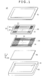
- Figure 1 is an exploded perspective view showing an example of a position detector including a first embodiment of a position detecting sensor according to the present invention.
- the example shown in Figure 1 illustrates a construction of a tablet device, including a position detecting sensor for detecting a position on a display surface of a display device indicated by, for example, a pen (stylus).
- the tablet device 10 of the example is composed of the position detecting sensor 20, a Liquid Crystal Display (LCD) device 30 as an example of the display device, a printed wiring board 40, and an upper case 51 and a lower case 52 that form a chassis of the tablet device 10.
- LCD Liquid Crystal Display
- the LCD 30 includes a display surface 33, on which a large number of display pixels 32 are disposed in the X-axis direction (in a transverse or horizontal direction) on an LCD substrate 31, and a large number of display pixels 32 are also disposed in the Y-axis direction (in a longitudinal or vertical direction) crossing at right angles with the X-axis direction on the LCD substrate 31.
- the position detecting sensor 20 is disposed so as to be superposed on the display surface 33 of the LCD 30.
- the position detecting sensor 20 adopts a construction of a sensor utilizing a cross-point capacitive system.
- the position detecting sensor 20 is constructed in such a way that a transparent electrode group 22 composed of plural electrodes each having light permeability is formed on one surface (a surface on a side opposite to a surface facing the display surface 33 of the LCD 30) of a transparent substrate 21. Also disposed on the display surface 33 are dummy patterns 23 each having predetermined light permeability.
- the transparent substrate 21 is composed, for example, of a glass substrate.
- the transparent electrode group 22 is composed of plural first transparent electrodes 24 disposed so as to each extend in the Y-axis direction, and plural second transparent electrodes 25 disposed so as to each extend in the X-axis direction crossing at right angles with the Y-axis direction.
- the first transparent electrodes 24 are disposed at predetermined intervals in the X-axis direction.
- the second transparent electrodes 25 are disposed at predetermined intervals in the Y-axis direction.
- Each of the first transparent electrodes 24 and the second transparent electrodes 25 is composed of a conductor made of a light-permeable conductive material, for example, of an ITO film.
- the first transparent electrodes 24 and the second transparent electrodes 25, in this example, are formed on the same one surface side of the transparent substrate 21. For this reason, at each of the cross-points where the first transparent electrodes 24 and the second transparent electrodes 25 intersect each other at right angles, an insulating material is disposed between each of the first transparent electrodes 24 and the corresponding second transparent electrode 25, whereby the first transparent electrodes 24 and the second transparent electrodes 25 are electrically insulated from each other. A detailed structure of the insulation between the first transparent electrodes 24 and the second transparent electrodes 25 in the area of the cross-point will be described later.
- the dummy pattern 23 is provided in an area surrounded by two adjacent first transparent electrodes 24 and two adjacent second transparent electrodes 25.
- the dummy pattern 23 is provided to equalize the light transmittance of an area, in which none of the first transparent electrode 24 and the second transparent electrode 25 is formed, with that of an area in which the first transparent electrode 24 and the second transparent electrode 25 are formed, to thereby attain uniform optical characteristics for the sensor substrate.
- the dummy pattern 23 should only be made of a material having a transmittance which is identical or comparable to that of each of the first transparent electrode 24 and the second transparent electrode 25, and thus the dummy pattern 23 needs not to be composed of a conductive member.
- the dummy pattern 23 is also composed of an ITO film used as the material for forming each of the first transparent electrode 24 and the second transparent electrode 25, in consideration of uniformity of the light transmittance and ease of manufacturing the position detecting sensor 20.
- the dummy pattern 23 is disposed with a predetermined space provided from each of the first transparent electrodes 24 and the second transparent electrodes 25, and is electrically independent of each of the first transparent electrodes 24 and the second transparent electrodes 25. Also, the dummy pattern 23 provided in the area surrounded by the first transparent electrodes 24 and the corresponding second transparent electrodes 25 is held in an electrically floating state (in a floating state).
- a sensor circuit portion (not shown in Figure 1 ) serving as a signal processing circuit portion is provided on the transparent substrate 21, on which the first transparent electrodes 24, the second transparent electrodes 25, and the dummy patterns 23 are all disposed in the manner as described above.
- the sensor circuit portion includes a transmission signal generating circuit 201, a transmission electrode selecting circuit 202, a reception electrode selecting circuit 203, a received signal processing circuit 204, an output circuit 205, and a control circuit 206.
- the transmission signal generating circuit 201 and the transmission electrode selecting circuit 202 compose a transmission signal supplying circuit
- the reception electrode selecting circuit 203 and the received signal processing circuit 204 compose a signal receiving circuit.
- each of the first transparent electrodes 24 is used as a reception electrode
- each of the second transparent electrodes 25 is used as a transmission electrode.
- the transmission signal generating circuit 201 supplies a predetermined transmission signal to the transmission electrode selecting circuit 202 at a timing controlled by the control circuit 206.
- the transmission electrode selecting circuit 202 selects predetermined second transparent electrodes 25 in accordance with the selection control by the control circuit 206.
- a transmission signal is supplied from the transmission signal generating circuit 201 to each of the second transparent electrodes 25 selected by the transmission electrode selecting circuit 202.
- the reception electrode selecting circuit 203 successively selects the first transparent electrodes 24 in accordance with the control by the control circuit 206, and successively supplies received signals from the first transparent electrodes 24 thus selected to the received signal processing circuit 204.
- the received signal processing circuit 204 processes the received signal in accordance with the control by the control circuit 206, detects a signal change caused by a position indicating operation of the indication body, such as a finger or a position indicator, on the position detecting sensor via the first transparent electrode 24, and supplies a detection output to the output circuit 205.
- a position indicating operation of the indication body such as a finger or a position indicator
- the output circuit 205 generates and outputs a detection signal corresponding to the position indicated by the indication body, such as the finger or the position indicator, based on detection of the first transparent electrode 24, in which the signal change is generated, from the detection output from the received signal processing circuit 204 and the second transparent electrode 25, to which the transmission signal is supplied at that time, in accordance with the control by the control circuit 206.
- the printed wiring board 40 Mounted on the printed wiring board 40 are an Integrated Circuit (IC) for controlling the tablet device 10, other electronic components, and a copper foil wiring pattern.
- IC Integrated Circuit
- the printed wiring board 40 is provided with a connector (not shown), through which the printed wiring board 40 is connected to a sensor circuit of the sensor 20 described above and a display drive circuit of the LCD 30.
- the upper case 51 and the lower case 52 composing the chassis of the tablet device 10 are made, for example, of synthetic resins.
- a concave portion 53 is formed in the lower case 52 of the chassis, for accommodating therein the transparent substrate 21, on which the position detecting sensor 20 is provided in position, the LCD substrate 31, and the printed wiring board 40. After the transparent substrate 21, on which the position detecting sensor 20 is provided in position, the LCD substrate 31, and the printed wiring board 40 are accommodated in the concave portion 53, the upper case 51 is adhered to the lower case 52 by, for example, using an adhesive agent to cover the concave portion 53, thereby assembling the tablet device 10.
- an ITO film is uniformly formed on a predetermined area on one surface of the transparent substrate 21.
- a mask pattern is used for the ITO film and, for example, a photolithography process is carried out by using the mask pattern, whereby an electrode pattern having the grid structure is formed.
- the first transparent electrodes 24 and the second transparent electrodes 25, and the dummy patterns 23 which are electrically independent of each of the first transparent electrodes 24 and the second transparent electrodes 25 and each of which is held in the electrically floating state, all composed of the ITO film, are formed at the same time.
- Figure 3 shows only a portion of the transparent electrode group 22 composed of three of the first transparent electrodes 24 and three of the second transparent electrodes 25, and also shows the structures of the first transparent electrodes 24, the second transparent electrodes 25, and the dummy patterns 23 in detail.
- the first transparent electrodes 24 are formed as the conductive members each extending in the Y-axis direction and having a predetermined outline, as will be described later, and are disposed on the transparent substrate 21 at the predetermined intervals in the X-axis direction.
- the second transparent electrodes 25 are formed as the conductive members each having a given width Wy and extending in the X-axis direction, and are disposed on the transparent substrate 21 at the predetermined intervals in the Y-axis direction.
- plural conductive member pieces 25P are disposed on the transparent substrate 21 in the X-axis direction, which are electrically separated from one another at portions where the first transparent electrodes 24 exist.
- an insulating layer (not shown) is formed in the intersection portion between each of the first transparent electrodes 24 and the corresponding second transparent electrode 25 by, for example, carrying out the photolithography process.
- a conductive layer 26 is formed for electrically connecting (bridging) two adjacent conductive member pieces 25P in the X-axis direction on the insulating layer by, for example, carrying out the photolithography process in a state in which the insulation between the corresponding ones of the first transparent electrodes 24 and the conductive layer 26 is maintained by the insulation layer.
- each of the plural conductive member pieces 25P disposed in the X-axis direction is electrically connected to one another, thereby forming the second transparent electrodes 25 extending in the X-axis direction.
- a width of the first transparent electrode 24 is narrowed and a width of the conductive member piece 25P forming the second transparent electrode 25 is also narrowed, and each of the insulating layer and the conductive layer 26 is formed as small as possible.
- the device is made such that the light transmittance of each cross-point portion where each of the first transparent electrodes 24 and the corresponding second transparent electrode 25 cross each other is made to vary as little as possible to be inconspicuous from that of other portions of the sensor substrate 21.
- an example shown in Figure 3 corresponds to the case where each of an outline of the electrode pattern of the first transparent electrodes 24, and an outline extending in the Y-axis direction of the dummy patterns 23, serves to decrease the Moire effect caused between the pixel disposition pattern of the LCD 30 in the Y-axis direction and the pattern of the first transparent electrodes 24.
- the sub-pixels corresponding to the same color are disposed in a line in the Y-axis direction. Therefore, the Moire effect is easily and conspicuously generated between the pixel disposition in the Y-axis direction, and the first transparent electrodes 24 extending in the Y-axis direction in the position detecting sensor 20.
- each of the outline of the electrode pattern of the second transparent electrodes 25 extending in the X-axis direction, and the outline of the dummy pattern 23 extending in the X-axis direction can be equally applied to address (decrease) the Moire effect generated between a pixel disposition in the X-axis direction of the LCD 30 and the conductor pattern.
- an area defined by four cross-points, where two adjacent first transparent electrodes 24 and two adjacent second transparent electrodes 25 cross each other, has a generally rectangular shape.
- the positions of the cross-points of the position detecting sensor 20 can be located along the straight lines in the Y-axis direction and in the X-axis direction, respectively. As a result, it becomes unnecessary to execute any position correction processing during the position detection calculation operation, and thus the position detection operation becomes easier.
- the first transparent electrode 24 is formed so as to have a predetermined electrode pattern between two cross-points disposed along the Y-axis direction.
- the first transparent electrode 24 has a shape, which has a predetermined inclination (or a tilt) with respect to the Y-axis direction, and which is line-symmetric about a straight line in the Y-axis direction. Specifically, as shown in Figure 3 , the first transparent electrode 24 has the shape defined by two contours 241 and 242 extending in the Y-axis direction. In this case, the two contours 241 and 242 of the first transparent electrode 24 extending in the Y-axis direction are made nonparallel with the Y-axis direction.
- the contour 241 and the contour 242 have a structure, in which line segments 241a and 242a each inclining at + ⁇ ( ⁇ > 0) with respect to the Y-axis direction, and line segments 241b and 242b each inclining at - ⁇ with respect to the Y-axis direction are connected to each other.
- the contour 241 and the contour 242 are formed in such a way that the line segment 241a inclining at + ⁇ with respect to the Y-axis direction and the line segment 242b inclining at - ⁇ with respect to the Y-axis direction face each other in the X-axis direction, and the line segment 241b inclining at - ⁇ with respect to the Y-axis direction and the line segment 242a inclining at + ⁇ with respect to the Y-axis direction face each other in the X-axis direction.
- the inclination angle ⁇ , with respect to the Y-axis direction, of the line segments 241a, 241b, and 242a, 242b composing the contours 241 and 242, respectively, of the first transparent electrode 24 can be considered as an angle relative to the longitudinal direction, in which the same sub-pixels are disposed in the LCD 30.
- the inclination angle ⁇ is suitably selected in order to prevent generation of the Moire fringes.
- the inclination angle ⁇ was set in the range equal to or larger than 5 degrees and equal to or smaller than 45 degrees, the effect of preventing generation of the Moire fringes was visually confirmed.
- each of the first transparent electrodes 24 is structured so as to have a shape that is line-symmetric about the central line 243 as the axis of symmetry, which is a straight line parallel with the Y-axis direction.
- the same circuit as that which is used when the first transparent electrode 24 has a straight (linear) pattern having a constant width can be used as the received signal processing circuit 204 when the first transparent electrode 24 is used as the reception electrode. Thus, it is unnecessary to perform position correcting processing or the like based on an indicated position.
- the first transparent electrode 24 has the shape, in which the line segments 241a and 242a each inclining at + ⁇ with respect to the Y-axis direction, and the line segments 241b and 242b each inclining at - ⁇ with respect to the Y-axis direction, are repetitively disposed plural times, in this example, twice in the Y-axis direction between two adjacent cross-points.
- the first transparent electrode 24 has at least one structure having both of the inclinations inclining at + ⁇ and - ⁇ with respect to the Y-axis direction, respectively, between two adjacent cross-points disposed in the Y-axis direction.
- the first transparent electrode 24 has only one shape having both of the inclinations inclining at + ⁇ and - ⁇ with respect to the Y-axis direction, respectively, between two adjacent cross-points disposed in the Y-axis direction, a maximum value of the width Wx of the first transparent electrode 24 becomes large, and thus a noise becomes easily detectable.
- the contours 241 and 242 in the Y-axis direction of the first transparent electrode 24 become approximately straight lines parallel with the Y-axis direction, to thereby lose some of the effect of preventing the Moire effect.
- the first transparent electrode 24 it is desirable for the first transparent electrode 24 to have a structure in which the shape having both of the inclination angles of + ⁇ and - ⁇ with respect to the Y-axis direction, respectively, is repeated twice or more, but less than a number of times at which the Moire preventing effect starts to lessen, between two adjacent cross-points disposed in the Y-axis direction as measures against both the noise and the Moire effect.
- the second transparent electrode 25 (the conductive member pieces 25P) disposed in the X-axis direction has a shape defined by two contours 251 and 252 extending in the X-axis direction.
- the sub-pixels corresponding to the same color are disposed in a line in the Y-axis direction. For this reason, it is known that the Moire effect is not as likely to occur between the pixels 32 of the LCD 30 disposed in the X-axis direction and the second transparent electrodes 25, as with the case of the first transparent electrodes 24.
- each of the contours 251 and 252 of the second transparent electrode 25 extending in the X-axis direction may be made as a straight line, and the second transparent electrode 25 is composed of a conductive member such as an ITO film having a given width Wy similarly to the conventional case.
- outlines of the dummy pattern 23 in the Y-axis direction are defmed by two contours 231 and 232 disposed close to the contours 242 and 241 of the first transparent electrode 24, respectively.
- outlines of the dummy pattern 23 extending in the X-axis direction are defined by two contours 233 and 234 disposed close to the contours 252 and 251 of the second transparent electrode 25, respectively.
- the two contours 231 and 232 extending in the Y-axis direction of the dummy pattern 23 are formed with spaces 27 each having a predetermined width from the two contours 242 and 241 of the first transparent electrode 24, respectively, so as to attain uniform optical characteristics for the position detecting sensor 20. Therefore, the two contours 231 and 232 extending along the Y-axis direction of the dummy pattern 23 have shapes, in which line segments 231a and 232a each inclining at + ⁇ with respect to the Y-axis direction, and line segments 231b and 232b each inclining at - ⁇ with respect to the Y-axis direction, are continuously connected to each other, respectively. It is noted that the space 27 is formed with a given width.
- Two contours 233 and 234 extending in the X-direction of the dummy pattern 23, and two contours 252 and 251 of the two adjacent second transparent electrodes 25 which hold the dummy pattern 23 between them in the Y-axis direction, are formed with spaces 28 therebetween each having a predetermined width. It is noted that the space 28 is formed with a given width.
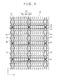
- Figure 4 shows an example of a positional relationship among the pixel disposition pattern, the electrode pattern of the first transparent electrodes 24 and the second transparent electrodes 25, and the dummy patterns 23 when the position detecting sensor 20 is superposed on the display surface 33 of the LCD 30.
- sub-pixels 34R, 34G, and 34B corresponding to the three primary colors: red; green; and blue and composing the pixel 32 are repetitively disposed in order in the same row in the X-axis direction (in the transverse direction).
- the same sub-pixel is repetitively disposed in the same column in the Y-axis direction, thereby composing the display surface 33 of the LCD 30.
- the sub-pixels 34R, 34G, and 34B each corresponding to the same color are disposed in a line in the Y-axis direction.
- the Moire effect is likely to occur between the pixel disposition in the Y-axis direction and the first transparent electrodes 24 extending in the Y-axis direction of the sensor 20.
- the contours of each of the first transparent electrodes 24 extending in the Y-axis direction have the shapes having the predetermined inclination angles of + ⁇ and - ⁇ with respect to the Y-axis direction, respectively.
- the dummy pattern 23 disposed close to the first transparent electrode 24 via the space 27 so as to attain uniform optical characteristics for the position detecting sensor 20 also has the predetermined inclination angles of + ⁇ and - ⁇ with respect to the Y-axis direction, respectively. Therefore, generation of the Moire fringes is reduced or prevented between the disposition pattern in the Y-axis direction of the display pixels 32 of the LCD 30 and the electrode pattern of the sensor 20.
- the shape of the area formed by the four cross-points at which two adjacent first transparent electrodes 24 and two adjacent second transparent electrodes 25 cross each other is maintained as a rectangular shape even when the measures against the Moire effect are taken.
- it is unnecessary to execute any position correction processing based on a position indication made by the indication body, which would otherwise be needed when the area does not have a rectangular shape.
- each of the first transparent electrodes 24 extending in the Y-axis direction has a shape that is line-symmetric about a straight central line 243, which is formed in the Y-axis direction by connecting the central points of the (varying) width Wx that extend in the X-axis direction, as the axis of symmetry. Therefore, the same circuit as that which is used when each of the first transparent electrodes 24 has a straight (linear) line pattern having a given (fixed) width in the X-axis direction can be used as the received signal processing circuit 204 for receiving the signal from the first transparent electrode 24 used as a reception electrode. As a result, it is unnecessary to execute position correction processing, which is typically required when a reception electrode does not having a given (fixed) width in the X-axis direction.
- the inclination angles ⁇ are set identical to one another in the plural first transparent electrodes 24, though it is obvious that the inclination angles ⁇ need not be identical to one another in all of the plural first transparent electrodes 24.
- first transparent electrodes 24 having different inclination angles are by no means limited to the case where every other first transparent electrode 24 along the X-axis direction has different inclination angles, and it is possible to have every two or more electrodes 24 have different inclination angles, for example.
- a portion of the first transparent electrode 24 located between two adjacent cross-points disposed in the Y-axis direction has a structure in which the contours composed of the line segment inclining at + ⁇ with respect to the Y-axis direction, and the line segment inclining at - ⁇ with respect to the Y-axis direction, are repetitively disposed twice.
- contours composed of the line segment inclining at + ⁇ with respect to the Y-axis direction and the line segment inclining at - ⁇ with respect to the Y-axis direction it is possible to provide contours composed of line segments having inclination angles that are not + ⁇ and - ⁇ .
- a predetermined space is formed between the contours 241 and 242 extending in the Y-axis direction of the first transparent electrode 24 and the contours 232 and 231 of the dummy pattern 23 facing the contours 241 and 242, respectively.
- a desired value can be selected as the width of the space, as long as determined uniform optical characteristics can be ensured for the position detecting sensor 20.
- the width of the space need not be constant. In other words, as described above, in accordance with various embodiments of the present invention, it is only necessary for the dummy pattern 23 to have contours including determined inclination angles with respect to the disposition of the pixels 32 of the LCD 30 along the Y-axis direction.
- the present invention can be also applied to the outlines extending in the X-axis direction, as defined by the shape (contours) of each of the second transparent electrodes 25 extending in the X-axis direction and the contours 233 and 234 extending in the X-axis direction of the dummy pattern 23.
- the present invention can be also applied to the outlines extending in the X-axis direction, as defined by the shape (contours) of each of the second transparent electrodes 25 extending in the X-axis direction and the contours 233 and 234 extending in the X-axis direction of the dummy pattern 23.
- the present invention can be also applied to the outlines extending in the X-axis direction, as defined by the shape (contours) of each of the second transparent electrodes 25 extending in the X-axis direction and the contours 233 and 234 extending in the X-axis direction of the dummy pattern 23.
- a capacitance change that occurs when the indication body, such as a finger or a position indicator, comes close to or in contact with the sensor 20 is detected relative to the coupling capacitance between the first transparent electrode 24 and the corresponding second transparent electrode 25. Therefore, when the coupling capacitance between the first transparent electrode 24 and the corresponding second transparent electrode 25 becomes large, it becomes difficult to detect a capacitance change that occurs when the indication body comes close to or in contact with the sensor 20.
- a divided dummy pattern DP composed of plural small dummy patterns, into which the dummy pattern 23 is divided, is provided in the area surrounded by the two adjacent first transparent electrodes 24 and the two adjacent transparent electrodes 25, instead of the dummy pattern 23 composed of one unitary area.
- the coupling capacitance between the first transparent electrode 24 and the corresponding second transparent electrode 25 can be regarded as a capacitance of plural capacitors that are connected in series with one another.
- the coupling capacitance it becomes possible to reduce the coupling capacitance as compared with the case of the dummy pattern 23 composed of one unitary area. Therefore, it becomes easier to detect a capacitance change that occurs when the indication body, such as a finger or a position indicator, comes close to or comes in contact with the position detecting sensor, and thus it is possible to increase the position detection sensitivity.
- the Moire effect might occur between contours (outlines) of the small dummy patterns and the disposition pattern of the pixels 32 of the LCD 30.
- measures are taken to reduce or prevent the Moire effect from occurring between the disposition pattern of the pixels 32 of the LCD 30 and the contours of the small dummy patterns.
- Figure 5 shows an example of a pattern shape of the electrode pattern having the grid structure, which includes the first transparent electrodes 24 and the second transparent electrodes 25 and the divided dummy pattern DP, in a position detecting sensor 60 of the second embodiment.
- a position detecting sensor 60 of the second embodiment shown in Figure 5 portions having the same structures as those in the position detecting sensor 20 of the first embodiment described above are designated by the same reference symbols, respectively, and detailed description thereof is omitted.
- the Moire effect may occur between the disposition of the pixels 32 of the LCD 30 extending in the Y-axis direction and the electrode pattern of the small dummy patterns in the position detecting sensor 60, and measures to be taken against generation of the Moire effect will now be described.
- the first transparent electrodes 24 and the second transparent electrodes 25 have the electrode patterns having the same shapes as those in the case of the first embodiment described above.
- the divided dummy pattern DP is provided by combining two kinds of parallelogram-like small dummy patterns 61 and 62, and two kinds of triangle-like small dummy patterns 63 and 64.
- the small dummy pattern 61 has a parallelogram-like shape, which is surrounded by contours 611 and 612 each parallel with the X-axis direction and contours 613 and 614 each having an inclination angle of - ⁇ with respect to the Y-axis direction.
- the small dummy pattern 62 has a parallelogram-like shape, which is surrounded by contours 621 and 622 parallel with the X-axis direction and contours 623 and 624 each having an inclination angle of + ⁇ with respect to the Y-axis direction.
- the small dummy pattern 63 has a triangle-like shape, which is surrounded by a contour 631 parallel with the X-axis direction, a contour 632 having an inclination angle of + ⁇ with respect to the Y-axis direction, and a contour 633 having an inclination angle of - ⁇ with respect to the Y-axis direction.
- the small dummy pattern 64 has a triangle-like shape, which is surrounded by a contour 641 parallel with the X-axis direction, a contour 642 having an inclination angle of + ⁇ with respect to the Y-axis direction, and a contour 643 having an inclination angle of - ⁇ with respect to the Y-axis direction.
- the triangle-like small dummy pattern 63 is disposed so as to have a vertex located downward
- the triangle-like small dummy pattern 64 is disposed so as to have a vertex located upward, as shown in Figure 5 .
- the contours 613 and 614 in the Y-axis direction of the parallelogram-like small dummy pattern 61 become parallel with the line segments 241b and 242b each having the inclination of - ⁇ with respect to the Y-axis direction, which form the contours 241 and 242 of the first transparent electrode 24, respectively.
- the contours 623 and 624 in the Y-axis direction of the parallelogram-like small dummy pattern 62 become parallel with the line segments 241a and 242a each having the inclination of + ⁇ with respect to the Y-axis direction, which form the contours 241 and 242 of the first transparent electrode 24, respectively.
- the contours 632 and 642 of the triangle-like small dummy patterns 63 and 64 become parallel with the line segments 241a and 242a, each having the inclination of + ⁇ with respect to the Y-axis direction, which form the contours 241 and 242 of the first transparent electrode 24, respectively. Also, the contours 633 and 643 of the triangle-like small dummy patterns 63 and 64 become parallel with the line segments 241b and 242b each having the inclination of - ⁇ with respect to the Y-axis direction, which form the contours 241 and 242 of the first transparent electrode 24, respectively.
- two parallelogram-like small dummy patterns 61 and two parallelogram-like small dummy patterns 62 and one triangle-like small dummy pattern 63 or 64 are disposed in the X-axis direction.
- this disposition pattern is repeated in four rows, to thereby form the structure in the Y-axis direction.
- the triangle-like small dummy patterns 63 and 64 are provided along the Y-axis direction at the center in the X-axis direction in the disposition of the divided dummy pattern DP.
- These small dummy patterns 61, 62, 63, and 64 are formed so as to electrically float. In other words, these small dummy patterns 61, 62, 63, and 64 are formed so as to have predetermined spaces from the first transparent electrodes 24 and the second transparent electrodes 25. Also, these small dummy patterns 61, 62, 63, and 64 are formed so as to have predetermined spaces from each other, i.e., among the small dummy patterns 61, 62, 63, and 64.
- a mask pattern is used for an ITO film formed over the entire surface of the transparent substrate 21, and the divided dummy patterns DP are then formed together with the first and second transparent electrodes 24 and 25 by carrying out the photolithography process.
- the divided dummy pattern DP in the second embodiment has a structure, which is point-symmetric about a central point in both the X-axis direction and the Y-axis direction of the area occupied by the divided dummy pattern DP. Therefore, the divided dummy patterns DP have the structure, which is point-symmetric about each of the intersection points (cross-points) between the first transparent electrodes 24 and the second transparent electrodes 25.
- each of the divided dummy patterns DP is structured so as to have the shape which is line-symmetric about the central line extending in the X-axis direction of the area occupied by the corresponding one of the divided dummy patterns DP, and is also structured so as to have the shape which is line-symmetric about the central line extending in the Y-axis direction of that area as the axis of symmetry.
- the divided dummy patterns DP have the pattern shape which is point-symmetric about each of the intersection points (cross-points) defined by the first transparent electrodes 24 and the second transparent electrodes 25. Therefore, according to the second embodiment, the position detection characteristics become uniform in all of the cross-points, and thus uniform sensor characteristics are obtained for the entire detection area of the sensor 20 (60).
- the pattern shapes of the divided dummy patterns DP should be vertically symmetric about the second transparent electrode 25 as the axis of symmetry.
- the pattern shapes of the divided dummy patterns DP should be horizontally symmetric about the first transparent electrode 24 as the axis of symmetry.
- the divided dummy patterns DP are structured so as to have the pattern shapes as described above, whereby according to the second embodiment, it is possible to obtain the same effects as those in the first embodiment. Also, since line segments formed by the contours 241 and 242 of the first transparent electrode 24, and the contours 613, 614, 623, 624, 632, 633, 642, 643 in the Y-axis direction of the small dummy patterns 61, 62, 63, and 64 have predetermined inclinations with respect to the Y-axis direction, generation of the Moire fringes between these line segments and the disposition pattern in the Y-axis direction of the pixels 32 of the LCD 30 is either decreased or prevented.
- the second embodiment has been described in such a way that the contours with respect to the Y-axis direction of the plural small dummy patterns 61, 62, 63, and 64 have the inclinations of ⁇ in the divided dummy patterns DP.
- the divided dummy pattern DP it is only necessary for the divided dummy pattern DP to have a shape corresponding to the shapes of the first transparent electrodes 24 and the second transparent electrodes 25, respectively, so that uniform transmittance can be ensured for the entire position detecting sensor 60.
- the dummy pattern DP is structured so as to have the shape which is line-symmetric about the central line in the X-axis direction of the area occupied by the dummy pattern DP, and is also line-symmetric about the central line in the Y-axis direction, and is further point-symmetric about the central point in the X-axis direction and in the Y-axis direction, it becomes possible to have uniform sensor characteristics over the entire sensor substrate.
- the contours 241 and 242 in the Y-axis direction of the first transparent electrode 24 are composed of the straight line segments 241a and 242a each having the predetermined inclination of + ⁇ with respect to the Y-axis direction and the straight line segments 241b and 242b each having the predetermined inclination of - ⁇ with respect to the Y-axis direction, whereby the contours of the plural first transparent electrodes 24 have the shapes having the respective predetermined inclinations with respect to the Y-axis direction.
- the present invention is by no means limited to the case where the shapes of the plural first transparent electrodes are composed of such straight line segments having the inclinations of 8 with respect to the Y-axis direction.
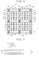
- a position detecting sensor 70 of an example shown in Figure 6 is a case where an arc-like curved line shape in the Y-axis direction, a so-called rounded shape, is used as a shape of a first transparent electrode to obtain a shape having a predetermined inclination with respect to the Y-axis direction.
- the position detecting sensor 70 of the example shown in Figure 6 is a case where the second embodiment is applied, in which a dummy pattern is formed as a divided dummy pattern. It is noted that, in the position detecting sensor 70 of the example shown in Figure 6 , portions having the same structures as those shown in the first embodiment described above are designated by the same reference symbols, respectively, and a detailed description thereof is omitted.
- first transparent electrodes 24R of an example shown in Figure 6 two contours in the Y-axis direction are composed of arc-like curved lines 241R and 242R, which are line-symmetric about a central line 243R of a width of the corresponding one of the first transparent electrodes 24R.
- the first transparent electrode 24R has a shape in which the arc-like curved lines 241R and 242R that are line-symmetric are repetitively disposed twice between two adjacent cross-points disposed in the Y-axis direction.
- the number of times the pattern disposition is repeated is set to two or more, but less than a number of times at which the Moire prevention effect may start to lessen, so as to achieve measures against both the Moire effect and the noise.
- a divided dummy pattern DPR of an example shown in Figure 6 is composed of six kinds of small dummy patterns 71, 72, 73, 74, 75, and 76 having respective shapes corresponding to the outline of the first transparent electrode 24R.
- any of the small dummy patterns 71, 72, 73, and 74 has two contours each composed of a straight line parallel with the X-axis direction.
- the small dummy pattern 71 further has contours of two curved lines parallel with the first-half curved line of the arc-like curved line 242R extending between two adjacent cross-points disposed in the Y-axis direction, and has a quadrangle-like shape surrounded by these contours of the two curved lines and the two straight lines parallel with the X-axis direction.
- the small dummy pattern 72 has contours of two curved lines parallel with the second-half curved line of the arc-like curved line 242R extending between two adjacent cross-points disposed in the Y-axis direction, and has a quadrangle-like shape surrounded by these contours of the two curved lines and the two straight lines parallel with the X-axis direction.
- the small dummy pattern 73 has contours of two curved lines parallel with the first-half curved line of the arc-like curved line 241R extending between two adjacent cross-points disposed in the Y-axis direction, and has a quadrangle-like shape surrounded by these contours of the two curved lines and the two straight lines parallel with the X-axis direction.
- the small dummy pattern 74 has contours of two curved lines parallel with the second-half curved line of the arc-like curved line 241R extending between two adjacent cross-points disposed in the Y-axis direction, and has a quadrangle-like shape surrounded by these contours of the two curved lines and the two straight lines parallel with the X-axis direction.
- the small dummy pattern 75 has a wedge-like shape surrounded by a contour parallel with the first-half curved line of the arc-like curved line 241R extending between two adjacent cross-points disposed in the Y-axis direction, a contour parallel with the first-half curved line of the arc-like curved line 242R extending between two adjacent cross-points disposed in the Y-axis direction, and a contour of a straight line parallel with the X-axis direction.
- the small dummy pattern 76 has a wedge-like shape surrounded by a contour parallel with the second-half curved line of the arc-like curved line 241R extending between two adjacent cross-points disposed in the Y-axis direction, a contour parallel with the second-half curved line of the arc-like curved line 242R extending between two adjacent cross-points disposed in the Y-axis direction, and a contour of a straight line parallel with the X-axis direction.
- the six kinds of small dummy patterns 71, 72, 73, 74, 75, and 76 are each composed of the same ITO film as that of each of the first transparent electrode 24R and the second transparent electrode 25, electrically independent of one another, and formed in an electrically floating state.
- the divided dummy patterns DPR are formed concurrently with the formation of the first transparent electrodes 24R and the second transparent electrodes 25 by carrying out the photolithography process.
- a first disposition pattern is formed, in which the small dummy pattern 71 is repetitively disposed twice in the X-axis direction, followed by the wedge-like small dummy pattern 75, which is in turn followed by the disposition of two of the small dummy patterns 73, and the first disposition pattern is repetitively disposed twice in the Y-axis direction.
- a second disposition pattern is formed, in which the small dummy pattern 72 is repetitively disposed twice in the X-axis direction, followed by the wedge-like small dummy pattern 76, which is in turn followed by the disposition of two of the small dummy patterns 74, and the second disposition pattern is repetitively disposed twice in the Y-axis direction.
- the divided dummy pattern DPR of the example shown in Figure 6 also has a structure which is point-symmetric about a central point in the X-axis direction and in the Y-axis direction of the area occupied by the divided dummy pattern DPR. Therefore, the divided dummy patterns DPR have the structure which is point-symmetric about each of the intersection points (cross-points) between the first transparent electrodes 24R and the second transparent electrodes 25. It is noted that the divided dummy pattern DPR is structured so as to have a shape which is line-symmetric about a central line in the X-axis direction of the area occupied by the divided dummy pattern DPR, and is also line-symmetric about the central line in the Y-axis direction of that area as the axis of symmetry.
- the first transparent electrodes, the second transparent electrodes, and the dummy patterns are all formed on one surface side of the transparent substrate
- both of the first and second transparent electrodes are provided on one surface of the transparent substrate, and the dummy patterns are formed on the other surface of the transparent substrate.
- the first transparent electrodes, the second transparent electrodes, and the dummy patterns are all formed on one surface side of the transparent substrate, there is an advantage that the number of processes required for manufacturing the position detecting sensor 20 is reduced, and thus the position detecting sensor 20 can be inexpensively manufactured.
- the first transparent electrodes, the second transparent electrodes, and the dummy patterns are separately formed on one surface and the other surface of the transparent substrate, a problem may arise that the visibility of the contours of the first transparent electrodes, the second transparent electrodes and the dummy patterns may vary depending on the thickness of the transparent substrate. Such problem can be avoided by forming all of the first transparent electrodes, the second transparent electrodes and the dummy patterns on one surface side of the transparent substrate.
- the present invention can also be applied in another system, in which the pixels are linearly disposed to construct a display device such as an LCD or an organic EL element, and a transparent position detecting sensor is disposed so as to be superposed on a display surface of the display device.
- the present invention can also be applied to a position detecting sensor 80 utilizing an electromagnetic induction system, as shown in Figures 7 and 8 .
- the position detecting sensor 80 utilizing the electromagnetic induction system of this example includes a detecting coil substrate 82, having light permeability and being superposed on a display surface 81D of a display device 81 such as an LCD, and a driving coil substrate 83 disposed on a side opposite to the display surface 81D of the display device 81.
- a position indicator 84 including a resonance circuit 841 is provided for use with the position detecting sensor 80 of this example.
- a driving coil is disposed on a substrate that is made of, for example, resin or the like. Since the driving coil substrate 83 is provided on a back surface side of the display device 81, it is not necessary to form the driving coil substrate or the driving coil with a transparent material.
- a signal having a predetermined frequency is supplied to the driving coil on the driving coil substrate 83 to generate an induced magnetic field, and an energy corresponding to the induced magnetic field is accumulated in the resonance circuit 841 of the position indicator 84. Then, the position indicator 84 supplies the magnetic field energy accumulated in the resonance circuit 841 to the detecting coil substrate 82.
- detecting loop coils 822X and 822Y each composed, for example, of an ITO film are formed in a grid, and a signal processing circuit portion 800 is provided in the periphery of the detecting loop coils 822X and 822Y.
- the detecting loop coils 822X include a long portion disposed in the Y-axis direction.
- the plural detecting loop coils 822X are disposed at predetermined intervals in the X-axis direction on the detecting coil substrate 82.
- the detecting loop coils 822Y include a long portion disposed in the X-axis direction.
- the plural detecting loop coils 822Y are disposed at predetermined intervals in the Y-axis direction on the detecting coil substrate 82.
- the signal processing circuit portion 800 includes selecting circuits 823X and 823Y, and a position calculating circuit 824.
- the selecting circuit 823X selects any one of the detecting loop coils 822X in accordance with the control by the position calculating circuit 824.
- the selecting circuit 823Y selects any one of the detecting loop coils 822Y in accordance with the control by the position calculating circuit 824.
- the position calculating circuit 824 detects a position indicated by the position indicator 84 in accordance with signals, which are received at the detecting loop coils 822X and 822Y selected by the selecting circuits 823X and 823Y, respectively. In other words, induced currents are caused to flow through the detecting loop coils 822X and 822Y, respectively, based on a magnetic field generated by the resonance circuit 841 of the position indicator 84.
- the position calculating circuit 824 determines the positions of the detecting loop coils 822X and 822Y, through which the induced currents are caused to flow, respectively, while switching the selecting circuits 823X and 823Y, and calculates the position indicated by the position indicator 84 based on the determined positions of the loop coils 822X and 822Y to output a signal corresponding to the calculated position.
- the detecting loop coils 822X and 822Y each composed of an ITO film are disposed in the X-axis direction and in the Y-axis direction, respectively, on the detecting coil substrate 82. Therefore, the detecting loop coils 822X and 822Y composed of the ITO film have shapes including predetermined contours, respectively.
- the Moire effect may occur between the pixels composing the display device 81 and the detecting loop coils 822X and 822Y. Therefore, the present invention can be applied not only to the position detecting sensor utilizing the capacitive system as described above, but also to the position detecting sensor utilizing the electromagnetic induction system having such a structure.
- a dummy pattern composed, for example, of an ITO film is provided in an area that exists between the detecting loop coils 822X and the detecting loop coils 822Y.
- the dummy pattern having a shape corresponding to contour shapes of conductive members of the detecting loop coils 822X and 822Y is applied in this example.
- the dummy pattern may also be structured as a divided dummy pattern composed of plural small dummy patterns as with the second embodiment.
- the driving coils are disposed on the driving coil substrate 83, and thus are disposed on a side opposite to the display surface 81D of the display device 81, alternatively, the driving coils can be disposed in the periphery on the display surface 81D side of the display device 81.
- the driving coils may also be disposed as circumferential exciting coil(s) 830 either on one surface of the detecting coil substrate 82 including the detecting loop coils 822X and 822Y disposed in the grid pattern, or in the circumference of the other surface of the detecting coil substrate 82.
- the circumferential exciting coil(s) 830 energy corresponding to the induced magnetic field is accumulated in the resonance circuit 841 of the position indicator 84, similarly to the case when the driving coils provided on the driving coil substrate 83 are used. Then, the position indicator 84 supplies the magnetic field energy accumulated in the resonance circuit 841 to the detecting coil substrate 82.
- the ITO film is used as the transparent conductive member, it is, of course, possible to use any other suitable transparent conductive material.
- the dummy pattern need not be made of the same transparent material as that of the conductive member composing the first transparent electrodes and the second transparent electrodes, and thus the dummy pattern may be made of a transparent material whose light transmittance is either equal or comparable to that of the first transparent electrode and the second transparent electrode.
- the dummy pattern need not be composed of a conductive member, the dummy pattern can be made, for example, of a nonconductive material such as a transparent resin or the like.
- the position detecting sensor of the present invention can also be applied, for example, in a portable terminal such as a cellular phone unit or a mobile personal computer, a stationary-type electronic apparatus, and other various kinds of electronic apparatus.
- the present invention is by no means limited to the LCD, and the present invention can be applied in various other types of display device, such as an organic electroluminescence display device, in which display pixels are regularly disposed.
Landscapes
- Engineering & Computer Science (AREA)
- General Engineering & Computer Science (AREA)
- Theoretical Computer Science (AREA)
- Physics & Mathematics (AREA)
- Human Computer Interaction (AREA)
- General Physics & Mathematics (AREA)
- Electromagnetism (AREA)
- Position Input By Displaying (AREA)
- Length Measuring Devices By Optical Means (AREA)
Applications Claiming Priority (1)
| Application Number | Priority Date | Filing Date | Title |
|---|---|---|---|
| JP2011155285A JP5777094B2 (ja) | 2011-07-14 | 2011-07-14 | 位置検出センサおよび位置検出装置 |
Publications (2)
| Publication Number | Publication Date |
|---|---|
| EP2546731A2 true EP2546731A2 (de) | 2013-01-16 |
| EP2546731A3 EP2546731A3 (de) | 2015-09-02 |
Family
ID=46458140
Family Applications (1)
| Application Number | Title | Priority Date | Filing Date |
|---|---|---|---|
| EP12169444.2A Withdrawn EP2546731A3 (de) | 2011-07-14 | 2012-05-25 | Positionserkennungssensor und Positionsdetektor |
Country Status (7)
| Country | Link |
|---|---|
| US (1) | US8885178B2 (de) |
| EP (1) | EP2546731A3 (de) |
| JP (1) | JP5777094B2 (de) |
| KR (1) | KR20130009608A (de) |
| CN (2) | CN202870788U (de) |
| IL (1) | IL219881A (de) |
| TW (1) | TWI550480B (de) |
Families Citing this family (31)
| Publication number | Priority date | Publication date | Assignee | Title |
|---|---|---|---|---|
| JP5777094B2 (ja) * | 2011-07-14 | 2015-09-09 | 株式会社ワコム | 位置検出センサおよび位置検出装置 |
| US20140015790A1 (en) * | 2012-07-11 | 2014-01-16 | J Touch Corporation | Capacitive touch control sensor |
| JP5826165B2 (ja) | 2012-12-28 | 2015-12-02 | 株式会社ジャパンディスプレイ | タッチ検出機能付き表示装置及び電子機器 |
| WO2014136455A1 (ja) * | 2013-03-07 | 2014-09-12 | 三菱電機株式会社 | 表示装置 |
| JP5865285B2 (ja) | 2013-03-27 | 2016-02-17 | 株式会社ジャパンディスプレイ | タッチ検出機能付き表示装置及び電子機器 |
| CN104102333B (zh) * | 2013-04-10 | 2017-04-12 | 宏碁股份有限公司 | 操作系统及其操作方法 |
| JP6131123B2 (ja) * | 2013-06-25 | 2017-05-17 | 株式会社ジャパンディスプレイ | タッチパネル付表示装置 |
| JP2015109067A (ja) * | 2013-10-22 | 2015-06-11 | パナソニックIpマネジメント株式会社 | 入力装置および表示装置 |
| WO2015118879A1 (ja) * | 2014-02-10 | 2015-08-13 | パナソニックIpマネジメント株式会社 | タッチパネル |
| KR101584423B1 (ko) * | 2014-02-21 | 2016-01-11 | 하이디스 테크놀로지 주식회사 | 모아레 감소를 위한 오버코트층을 구비한 터치 패널, 터치 패널을 구비한 액정표시장치 및 터치 패널 형성 방법 |
| KR101527320B1 (ko) * | 2014-02-26 | 2015-06-09 | 하이디스 테크놀로지 주식회사 | 매트릭스 스위칭 타입 터치패널 |
| JP6375678B2 (ja) * | 2014-04-24 | 2018-08-22 | 凸版印刷株式会社 | 磁気センサー |
| JP2015232819A (ja) * | 2014-06-10 | 2015-12-24 | 株式会社ジャパンディスプレイ | センサ付き表示装置 |
| KR102286730B1 (ko) * | 2014-06-13 | 2021-08-09 | 미래나노텍(주) | 비정형 센서 패턴을 구비한 터치 센서 및 이를 이용한 터치스크린 패널 |
| TWI552039B (zh) * | 2014-06-27 | 2016-10-01 | 群創光電股份有限公司 | 觸控顯示裝置 |
| KR101605622B1 (ko) * | 2014-07-15 | 2016-03-23 | 하이디스 테크놀로지 주식회사 | 터치 패널 |
| KR102318028B1 (ko) * | 2015-03-13 | 2021-10-27 | 삼성전자주식회사 | 디지타이저 회로 패터닝 방법 및 이를 지원하는 전자 장치 |
| TWI628567B (zh) * | 2015-05-28 | 2018-07-01 | 鴻海精密工業股份有限公司 | 觸控裝置 |
| US10064270B2 (en) * | 2015-06-05 | 2018-08-28 | North Carolina State University | Flexible interconnects, systems, and uses thereof |
| JPWO2017060936A1 (ja) * | 2015-10-06 | 2018-11-01 | ニューコムテクノ株式会社 | タッチセンサ |
| JP6639296B2 (ja) * | 2016-03-23 | 2020-02-05 | 株式会社ジャパンディスプレイ | 表示装置 |
| KR101919554B1 (ko) | 2016-04-28 | 2018-11-19 | 삼성디스플레이 주식회사 | 터치 표시 장치 및 이의 제조 방법 |
| KR102601650B1 (ko) * | 2016-07-26 | 2023-11-13 | 삼성디스플레이 주식회사 | 표시 장치 |
| CN106249963B (zh) * | 2016-09-29 | 2019-02-12 | 京东方科技集团股份有限公司 | 触控电极结构以及触控显示面板 |
| EP3564800A1 (de) * | 2016-12-28 | 2019-11-06 | Fujikura Ltd. | Verdrahtungskörper, verdrahtungsplatine und berührungssensor |
| CN108628483B (zh) * | 2017-03-15 | 2021-03-05 | 京东方科技集团股份有限公司 | 触控单元、互电容触控屏和触控显示装置 |
| JP6369589B1 (ja) * | 2017-03-30 | 2018-08-08 | Smk株式会社 | 静電容量式タッチパネル |
| JPWO2018193891A1 (ja) * | 2017-04-17 | 2020-02-27 | パナソニックIpマネジメント株式会社 | タッチセンサ |
| CN108415615B (zh) * | 2018-04-28 | 2020-07-28 | 京东方科技集团股份有限公司 | 金属网格、触摸屏和显示装置 |
| JP7395402B2 (ja) * | 2020-03-26 | 2023-12-11 | 株式会社ジャパンディスプレイ | 検出装置 |
| EP4239458A4 (de) | 2021-02-09 | 2024-02-21 | Samsung Electronics Co., Ltd. | Digitalisiertafel und elektronische vorrichtung mit der digitalisiertafel |
Family Cites Families (19)
| Publication number | Priority date | Publication date | Assignee | Title |
|---|---|---|---|---|
| JPH07109575B2 (ja) * | 1986-09-16 | 1995-11-22 | 株式会社ワコム | 位置指示器の状態検出方式 |
| JPH08202487A (ja) * | 1995-01-27 | 1996-08-09 | Totoku Electric Co Ltd | 透明型デジタイザセンサ板および電磁誘導方式デジタイザ |
| JPH11110115A (ja) * | 1997-09-30 | 1999-04-23 | Fujitsu General Ltd | デジタイザ装置 |
| JP2009009249A (ja) | 2007-06-26 | 2009-01-15 | Nissha Printing Co Ltd | 静電容量式タッチパネル及びこれを用いた2方式併用タッチパネル |
| JP5094376B2 (ja) * | 2007-12-28 | 2012-12-12 | 株式会社ワコム | 位置検出装置 |
| JP4945483B2 (ja) * | 2008-02-27 | 2012-06-06 | 株式会社 日立ディスプレイズ | 表示パネル |
| JP2009259063A (ja) * | 2008-04-18 | 2009-11-05 | Gunze Ltd | タッチパネルおよびその製造方法 |
| US20090273577A1 (en) * | 2008-04-30 | 2009-11-05 | Apple Inc. | Moire-Free Touch Screen with Tilted or Curved ITO Pattern |
| US8159467B2 (en) * | 2008-08-21 | 2012-04-17 | Wacom Co. Ltd. | Meshed touchscreen pattern |
| JP5491020B2 (ja) * | 2008-11-26 | 2014-05-14 | 株式会社ジャパンディスプレイ | タッチパネル |
| US8593410B2 (en) * | 2009-04-10 | 2013-11-26 | Apple Inc. | Touch sensor panel design |
| US9075484B2 (en) * | 2009-06-02 | 2015-07-07 | Pixart Imaging Inc. | Sensor patterns for mutual capacitance touchscreens |
| JP5295008B2 (ja) * | 2009-06-18 | 2013-09-18 | 株式会社ワコム | 指示体検出装置 |
| US8957874B2 (en) * | 2009-06-29 | 2015-02-17 | Apple Inc. | Touch sensor panel design |
| CN101630216B (zh) * | 2009-07-31 | 2012-06-27 | 深圳市旺博科技有限公司 | 一种柔性防干扰投射式电容触摸屏 |
| JP2011065450A (ja) * | 2009-09-17 | 2011-03-31 | Wacom Co Ltd | 位置検出装置及び位置指示器 |
| JP3167700U (ja) * | 2011-02-22 | 2011-05-12 | 洋華光電股▲ふん▼有限公司 | 透明タッチコントロールセンサー |
| JP2012194274A (ja) * | 2011-03-15 | 2012-10-11 | Japan Display West Co Ltd | 表示装置 |
| JP5777094B2 (ja) * | 2011-07-14 | 2015-09-09 | 株式会社ワコム | 位置検出センサおよび位置検出装置 |
-
2011
- 2011-07-14 JP JP2011155285A patent/JP5777094B2/ja active Active
-
2012
- 2012-05-01 US US13/461,177 patent/US8885178B2/en active Active
- 2012-05-17 IL IL219881A patent/IL219881A/en active IP Right Grant
- 2012-05-23 TW TW101118331A patent/TWI550480B/zh active
- 2012-05-25 EP EP12169444.2A patent/EP2546731A3/de not_active Withdrawn
- 2012-05-30 KR KR1020120057455A patent/KR20130009608A/ko not_active Withdrawn
- 2012-07-16 CN CN2012203440090U patent/CN202870788U/zh not_active Expired - Lifetime
- 2012-07-16 CN CN2012102458180A patent/CN102880365A/zh active Pending
Also Published As
| Publication number | Publication date |
|---|---|
| EP2546731A3 (de) | 2015-09-02 |
| US8885178B2 (en) | 2014-11-11 |
| JP2013020560A (ja) | 2013-01-31 |
| TW201308177A (zh) | 2013-02-16 |
| US20130016363A1 (en) | 2013-01-17 |
| KR20130009608A (ko) | 2013-01-23 |
| IL219881A (en) | 2016-06-30 |
| CN102880365A (zh) | 2013-01-16 |
| IL219881A0 (en) | 2012-07-31 |
| JP5777094B2 (ja) | 2015-09-09 |
| TWI550480B (zh) | 2016-09-21 |
| CN202870788U (zh) | 2013-04-10 |
Similar Documents
| Publication | Publication Date | Title |
|---|---|---|
| US8885178B2 (en) | Position detecting sensor and position detector | |
| US8077161B2 (en) | Screen-input image display device | |
| CN107193417B (zh) | 触控显示屏和显示装置 | |
| CN111665998B (zh) | 触控显示面板 | |
| CN104969154B (zh) | 用于在触摸屏设备中降低可见度的网格传感器设计 | |
| TWI441071B (zh) | 電容式觸碰感測器面板、包含其之電容式觸碰感測器系統及資訊輸入輸出元件 | |
| TWI460494B (zh) | 具有觸控式感測輸入元件的顯示裝置 | |
| US20120242606A1 (en) | Trace design for reduced visibility in touch screen devices | |
| US20120001867A1 (en) | Capacitance sensor and information input apparatus | |
| JP6494287B2 (ja) | タッチスクリーン、タッチパネル、表示装置、および電子機器 | |
| US10037109B2 (en) | Touch-panel substrate and electronic device with electrodes provided on different plane surfaces and reduced non-uniformity of in-plane light transmittance | |
| JP2007048278A (ja) | 電磁デジタイザセンサアレイ構造 | |
| CN106775050A (zh) | 触控显示面板及装置 | |
| US20150062449A1 (en) | Touch panel | |
| US9563324B2 (en) | Touch panel substrate, electronic device, and production method for electronic device | |
| JP2025084876A (ja) | 電子機器 | |
| JP6053571B2 (ja) | タッチスクリーン、タッチパネル及びそれを備える表示装置 | |
| US20130057790A1 (en) | Apparatus, Methods and Computer Programs for configuring Output of a Display | |
| US11334199B2 (en) | Spatially encoded sensor electrodes | |
| CN114585994B (zh) | 触控基板、触控模组及触控显示装置 | |
| EP3413178B1 (de) | Leitfähige folie, berührungsbildschirm und anzeigevorrichtung | |
| CN115605834B (zh) | 阵列基板及显示装置 | |
| CN118444802A (zh) | 触控面板及其制备方法和显示装置 |
Legal Events
| Date | Code | Title | Description |
|---|---|---|---|
| PUAI | Public reference made under article 153(3) epc to a published international application that has entered the european phase |
Free format text: ORIGINAL CODE: 0009012 |
|
| AK | Designated contracting states |
Kind code of ref document: A2 Designated state(s): AL AT BE BG CH CY CZ DE DK EE ES FI FR GB GR HR HU IE IS IT LI LT LU LV MC MK MT NL NO PL PT RO RS SE SI SK SM TR |
|
| AX | Request for extension of the european patent |
Extension state: BA ME |
|
| PUAL | Search report despatched |
Free format text: ORIGINAL CODE: 0009013 |
|
| AK | Designated contracting states |
Kind code of ref document: A3 Designated state(s): AL AT BE BG CH CY CZ DE DK EE ES FI FR GB GR HR HU IE IS IT LI LT LU LV MC MK MT NL NO PL PT RO RS SE SI SK SM TR |
|
| AX | Request for extension of the european patent |
Extension state: BA ME |
|
| RIC1 | Information provided on ipc code assigned before grant |
Ipc: G06F 3/046 20060101ALI20150729BHEP Ipc: G06F 3/044 20060101AFI20150729BHEP |
|
| 17P | Request for examination filed |
Effective date: 20160223 |
|
| RBV | Designated contracting states (corrected) |
Designated state(s): AL AT BE BG CH CY CZ DE DK EE ES FI FR GB GR HR HU IE IS IT LI LT LU LV MC MK MT NL NO PL PT RO RS SE SI SK SM TR |
|
| STAA | Information on the status of an ep patent application or granted ep patent |
Free format text: STATUS: THE APPLICATION HAS BEEN WITHDRAWN |
|
| 18W | Application withdrawn |
Effective date: 20170123 |