EP2545209B1 - Procede de preparation d'une couche mince d'absorbeur pour cellules photovoltaïques - Google Patents
Procede de preparation d'une couche mince d'absorbeur pour cellules photovoltaïques Download PDFInfo
- Publication number
- EP2545209B1 EP2545209B1 EP20110713307 EP11713307A EP2545209B1 EP 2545209 B1 EP2545209 B1 EP 2545209B1 EP 20110713307 EP20110713307 EP 20110713307 EP 11713307 A EP11713307 A EP 11713307A EP 2545209 B1 EP2545209 B1 EP 2545209B1
- Authority
- EP
- European Patent Office
- Prior art keywords
- equal
- mixture
- group
- layer
- thin film
- Prior art date
- Legal status (The legal status is an assumption and is not a legal conclusion. Google has not performed a legal analysis and makes no representation as to the accuracy of the status listed.)
- Active
Links
Images


Classifications
-
- C—CHEMISTRY; METALLURGY
- C25—ELECTROLYTIC OR ELECTROPHORETIC PROCESSES; APPARATUS THEREFOR
- C25D—PROCESSES FOR THE ELECTROLYTIC OR ELECTROPHORETIC PRODUCTION OF COATINGS; ELECTROFORMING; APPARATUS THEREFOR
- C25D3/00—Electroplating: Baths therefor
- C25D3/02—Electroplating: Baths therefor from solutions
- C25D3/56—Electroplating: Baths therefor from solutions of alloys
-
- C—CHEMISTRY; METALLURGY
- C25—ELECTROLYTIC OR ELECTROPHORETIC PROCESSES; APPARATUS THEREFOR
- C25D—PROCESSES FOR THE ELECTROLYTIC OR ELECTROPHORETIC PRODUCTION OF COATINGS; ELECTROFORMING; APPARATUS THEREFOR
- C25D11/00—Electrolytic coating by surface reaction, i.e. forming conversion layers
-
- C—CHEMISTRY; METALLURGY
- C25—ELECTROLYTIC OR ELECTROPHORETIC PROCESSES; APPARATUS THEREFOR
- C25D—PROCESSES FOR THE ELECTROLYTIC OR ELECTROPHORETIC PRODUCTION OF COATINGS; ELECTROFORMING; APPARATUS THEREFOR
- C25D3/00—Electroplating: Baths therefor
- C25D3/02—Electroplating: Baths therefor from solutions
- C25D3/56—Electroplating: Baths therefor from solutions of alloys
- C25D3/58—Electroplating: Baths therefor from solutions of alloys containing more than 50% by weight of copper
-
- C—CHEMISTRY; METALLURGY
- C25—ELECTROLYTIC OR ELECTROPHORETIC PROCESSES; APPARATUS THEREFOR
- C25D—PROCESSES FOR THE ELECTROLYTIC OR ELECTROPHORETIC PRODUCTION OF COATINGS; ELECTROFORMING; APPARATUS THEREFOR
- C25D9/00—Electrolytic coating other than with metals
- C25D9/04—Electrolytic coating other than with metals with inorganic materials
- C25D9/08—Electrolytic coating other than with metals with inorganic materials by cathodic processes
-
- H—ELECTRICITY
- H10—SEMICONDUCTOR DEVICES; ELECTRIC SOLID-STATE DEVICES NOT OTHERWISE PROVIDED FOR
- H10F—INORGANIC SEMICONDUCTOR DEVICES SENSITIVE TO INFRARED RADIATION, LIGHT, ELECTROMAGNETIC RADIATION OF SHORTER WAVELENGTH OR CORPUSCULAR RADIATION
- H10F10/00—Individual photovoltaic cells, e.g. solar cells
- H10F10/10—Individual photovoltaic cells, e.g. solar cells having potential barriers
- H10F10/16—Photovoltaic cells having only PN heterojunction potential barriers
- H10F10/167—Photovoltaic cells having only PN heterojunction potential barriers comprising Group I-III-VI materials, e.g. CdS/CuInSe2 [CIS] heterojunction photovoltaic cells
-
- H—ELECTRICITY
- H10—SEMICONDUCTOR DEVICES; ELECTRIC SOLID-STATE DEVICES NOT OTHERWISE PROVIDED FOR
- H10F—INORGANIC SEMICONDUCTOR DEVICES SENSITIVE TO INFRARED RADIATION, LIGHT, ELECTROMAGNETIC RADIATION OF SHORTER WAVELENGTH OR CORPUSCULAR RADIATION
- H10F77/00—Constructional details of devices covered by this subclass
- H10F77/10—Semiconductor bodies
- H10F77/12—Active materials
- H10F77/126—Active materials comprising only Group I-III-VI chalcopyrite materials, e.g. CuInSe2, CuGaSe2 or CuInGaSe2 [CIGS]
-
- H—ELECTRICITY
- H10—SEMICONDUCTOR DEVICES; ELECTRIC SOLID-STATE DEVICES NOT OTHERWISE PROVIDED FOR
- H10F—INORGANIC SEMICONDUCTOR DEVICES SENSITIVE TO INFRARED RADIATION, LIGHT, ELECTROMAGNETIC RADIATION OF SHORTER WAVELENGTH OR CORPUSCULAR RADIATION
- H10F77/00—Constructional details of devices covered by this subclass
- H10F77/30—Coatings
-
- Y—GENERAL TAGGING OF NEW TECHNOLOGICAL DEVELOPMENTS; GENERAL TAGGING OF CROSS-SECTIONAL TECHNOLOGIES SPANNING OVER SEVERAL SECTIONS OF THE IPC; TECHNICAL SUBJECTS COVERED BY FORMER USPC CROSS-REFERENCE ART COLLECTIONS [XRACs] AND DIGESTS
- Y02—TECHNOLOGIES OR APPLICATIONS FOR MITIGATION OR ADAPTATION AGAINST CLIMATE CHANGE
- Y02E—REDUCTION OF GREENHOUSE GAS [GHG] EMISSIONS, RELATED TO ENERGY GENERATION, TRANSMISSION OR DISTRIBUTION
- Y02E10/00—Energy generation through renewable energy sources
- Y02E10/50—Photovoltaic [PV] energy
- Y02E10/541—CuInSe2 material PV cells
Definitions
- the present invention relates to the manufacture of photovoltaic cells, in particular for the conversion of solar energy into electrical energy. More particularly, the present invention relates to a method for preparing a thin absorber layer for photovoltaic cells and a method of manufacturing a solar cell comprising a thin absorber layer prepared according to the invention.
- Photovoltaic cells often have a structure according to a stack of thin layers, at least one of these thin layers has photovoltaic properties.
- photovoltaic cell structure An example of photovoltaic cell structure is shown on the figure 1 .
- a photovoltaic cell generally has a stack of layers disposed on an insulating support 12.
- the insulating support 12 is a glass layer.
- molybdenum layer 14 On the insulating support 12 is deposited a layer of molybdenum 14 with a thickness of between 0.5 microns and 1 micron.
- the molybdenum layer 14 is generally deposited by evaporation under vacuum or spraying.
- An absorber layer 16 is deposited on the molybdenum layer 14.
- the absorber layer 16 generally has a thickness of about 2 microns and can be deposited by evaporation under vacuum or sputtering.
- An interfacial layer 18 is deposited on the absorber layer 16.
- the interfacial layer 18 also called the buffer layer, may comprise cadmium sulphide or zinc sulphide deposited by chemical means in solution.
- the interfacial layer 18 has a thickness generally between 10 nm and 80 nm.
- a lightly doped zinc oxide layer 20 is deposited by sputtering onto interfacial layer 18.
- the lightly doped zinc oxide layer 20 has a thickness of about 50 nm to 100 nm.
- An aluminum-doped zinc oxide layer 22 is deposited on the low-doped zinc oxide layer 20.
- the aluminum-doped zinc oxide layer 22 is conventionally deposited by vacuum spraying so as to have a thickness of about 0.5 microns to 1 micron.
- this zinc oxide layer is to render this n-type conductive layer and to serve as an electrode (transparent in the visible) on the front face of the photovoltaic cell.
- Photovoltaic cells whose absorber layer 16 consists of compounds of CuInSe 2 or Cu (In x , Ga 1-x ) Se 2 type , have conversion efficiencies of up to 20%.
- the main method of preparation of thin-film photovoltaic cells uses physical channels, for example co-evaporation or cathodic sputtering.
- the photovoltaic properties of CuInSe 2 or Cu (In x , Ga 1-x ) Se 2 thin films depend largely on the composition of the thin absorber layer. Thus, it is important to be able to control as precisely as possible the composition of the thin absorber layer.
- the document EP 0 574 716 A1 proposes a method for preparing a thin absorber layer for photovoltaic cells of type ABC 2 or A 2 - (D x , E 1-x ) -C 4 comprising steps of depositing oxides of elements A or B by laser ablation on a molybdenum substrate, and annealing under a reducing atmosphere comprising a group 16 element, at a temperature between 400 ° C and 600 ° C.
- the document GB 2,370,282 proposes a process for the preparation of a thin absorber layer for photovoltaic cells of the CIS or CIGS type comprising the steps of electroplating the unoxidized Cu, In and / or Ga elements on a molybdenum, selenization or sulphurization substrate, then annealing.
- Document XP000690723 is an article describing a method for preparing a thin absorber layer for CIS type photovoltaic cells comprising a step of electroplating all the elements of the layer, followed by annealing under vacuum at 400 ° C. .
- the document DE 196 30 321 discloses a method for preparing a thin absorber layer for CIS type photovoltaic cells comprising the steps of electroplating all elements of the layer followed by annealing at a temperature of between 100 ° C and 550 ° C.
- Electrochemical deposition is a process that can improve the control of composition of thin films of CuInSe 2 or Cu (In x , Ga 1-x ) Se 2 type .
- the electrochemical deposition of the elements of the groups 11, 12, 13, and 14 in the form of oxide and / or hydroxides is easier to achieve and allows better control of the final composition than the electrochemical deposition of these elements under non-oxidized form.
- the electrolyte solution is more stable when it is desired to form the oxides in the absence of elements Se or S in solution and unlike the electrochemical deposition of the prior art, the chemical composition of the absorber thin film does not evolve during the growth of said layer.
- the invention also relates to a method for manufacturing a solar cell, comprising a method for preparing a thin absorber layer for photovoltaic cells according to the invention.
- the invention relates to a method for preparing a thin absorber layer for photovoltaic cells.
- the thin absorber layer being based on an alloy of type ABC 2 or A 2 - (D x , E 1-x ) -C 4 with 0 x x 1 1 and A is an element or a mixture of elements selected from group 11, B is an element or element selected from group 13, C is an element or a mixture of elements selected from group 16, D is an element or a mixture of elements selected from group 12 and E is an element or mixture of elements selected from group 14.
- A is an element or a mixture of elements chosen from copper (Cu) and silver (Ag).
- B is an element or a mixture of elements chosen from aluminum (Al), gallium (Ga), and indium (In).
- C is an element or a mixture of elements chosen from sulfur (S) and selenium (Se).
- D is an element or a mixture of elements chosen from zinc (Zn) and cadmium (Cd).
- E is an element or a mixture of elements chosen from silicon (Si), germanium (Ge), tin (Sn) and lead (Pb).
- the absorber thin film is based on a Cu (In x Ga 1-x ) Se 2 type alloy with 0 x x 1 1 .
- the absorber thin film is based on a Cu 2 type alloy (Sn x Zn 1-x ) (Se y S 1-y ) 4 with 0 x x 1 1 and 0 ⁇ y ⁇ 1.
- the method comprises a step of preparing an electrolyte.
- the process according to the invention uses the deposition of oxide layer of elements A, B, D, or E.
- This deposition of the layer of oxides and / or hydroxides can be carried out by low-level electrolysis. temperature, higher or equal to 5 ° C and less than or equal to 95 ° C, and does not require expensive vacuum or vapor deposition apparatus.
- the electrolyte may, for example, be an aqueous solution containing a mixture of salts of A and B in order to prepare a preparation of a type ABC 2 layer or a mixture of salts of A, D and / or or E for a layer of type A 2 - (D x E 1-x ) -C 4 .
- the salts are mixed in the presence of an oxygen donor species.
- the salts of the elements A, B, D and E may be nitrates.
- the oxygen donor species may be nitrate, or oxygen gas or hydrogen peroxide or hypochlorite ions.
- the aqueous solution may also comprise a support electrolyte in order to increase its conductivity.
- the aqueous electrolyte solutions according to the invention are stable and show no tendency to precipitation.
- the electrochemical deposition can be done by applying to a deposit electrode a potential with respect to a reference electrode or a current density.
- the deposition electrode may comprise an insulating plate, for example a glass plate covered with a layer of molybdenum.
- the reference electrode may be a saturated calomel electrode or a mercurous sulfate electrode or an Ag / AgCl electrode.
- the electrochemical deposition is carried out at a temperature greater than or equal to 5 ° C. and less than or equal to 95 ° C., for example at a temperature greater than or equal to 30 ° C., preferably greater than or equal to 60 ° C. ° C and less than or equal to 83 ° C, for example substantially equal to 80 ° C.
- the element A is copper and the element B is chosen from indium, gallium and aluminum or one of their mixtures
- the electrochemical deposition is carried out by imposing on the electrode a potential with respect to a saturated mercurous sulfate reference electrode greater than or equal to -1.8 V, for example greater than or equal to -1V, and less than or equal to -0.5V, for example less than or equal to -0, 70 V. It is also possible to impose a current density of between 1.0 and 30 mAcm -2 .
- the oxide and / or hydroxide layer is deposited on the electrode comprising an insulating substrate covered with a layer of molybdenum in the form of a thin layer whose thickness is controlled by the quantity of electricity exchanged during the reaction, the reaction temperature and the reaction time.
- Deposition rates are high about 3.5 micrometers per hour at 25 ° C and more than 10 micrometers per hour at 80 ° C.
- the deposition is carried out in aqueous solution for a period of about 10 to 20 minutes and leads to the formation of an oxide layer having a thickness of between 600 and 2,000 nanometers, for example between 800 and 1,200 nanometers .
- composition of the deposited absorber layer is controlled on the one hand by the salt composition of the aqueous solution and by the potential or the current density imposed on the deposition electrode.
- photovoltaic cells obtained with absorber layers comprising alloys of type ABC 2 exhibit improved conversion efficiencies when the atomic ratio of elements A and B in the electrolyte solution. is greater than or equal to 0.2, for example greater than 0.8, and less than or equal to 1.5, for example less than or equal to 1.2, for example less than or equal to 1, for example substantially equal to 1 .
- the inventors have observed that the conversion efficiency is improved when the atomic ratio Cu / (In + Ga) is close of the unit and the gallium content: Ga / (In + Ga) is greater than or equal to 0.2 and less than or equal to 0.35, for example substantially equal to 0.3.
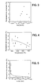
- the figure 3 illustrates the influence of the gallium content in the Cu (In x Ga 1-x ) S 2 absorber layer on the conversion efficiency of the photovoltaic cell comprising said absorber layer.
- the conversion efficiency is optimal for a gallium Ga / (In + Ga) content of between 0.2 and 0.35, preferably substantially equal to 0.3.
- the inventors have been able to observe by X-ray diffraction that the deposits of the oxides and / or hydroxides have an amorphous appearance.
- the method according to the invention further comprises a step of annealing under a reducing atmosphere of the thin oxide layer obtained during the electrochemical deposition.
- the figure 4 illustrates the influence of the temperature of the annealing step under a reducing atmosphere on the conversion efficiency of a photovoltaic cell comprising a Cu absorber layer (In x Ga 1-x ) S 2 , the step of annealing being carried out under an ethanol atmosphere for 20 seconds.
- the annealing step under a reducing atmosphere is carried out at a temperature greater than or equal to 300 ° C and less than or equal to 650 ° C, for example at a temperature greater than or equal to 500 ° C and less than or equal to 575 ° C, for example at a temperature substantially equal to 550 ° C.
- the annealing step under a reducing atmosphere can last between 20 seconds and 15 minutes, for example between 20 seconds and 5 minutes.
- the figure 5 illustrates the influence of the duration of the annealing step under a reducing atmosphere on the conversion efficiency of a photovoltaic cell comprising a Cu (In x Ga 1-x ) S 2 absorber layer, the step of annealing being carried out under an ethanol atmosphere at a temperature of 550 ° C.
- the annealing step under a reducing atmosphere lasts between 20 seconds and 50 seconds.
- the annealing step under a reducing atmosphere can be carried out using an H 2 / N 2 mixture or alcohol, hydrocarbon vapors or even ammonia vapors.
- the annealing step in a reducing atmosphere allows a reduction of the metal alloy oxide layer.
- the figure 6 is an X-ray diffraction pattern of a mixture of copper, gallium and indium oxide oxide after the annealing step under a reducing atmosphere.
- the diffraction pattern shown in FIG. figure 6 allows to distinguish a cubic phase of Cu 9 In 4 and Cu 9 Ga 4 type as well as a large peak corresponding to the molybdenum substrate.
- the diagram can be indexed as a mixed phase Cu 9 (In x , Ga 1-x ) 4 of cubic structure and an intermediate parameter between that of Cu 9 In 4 and Cu 9 Ga 4 .
- the method according to the invention further comprises a step of adding at least one element of group 16 so as to form a thin film of type ABC 2 or A 2 - (D x , E 1-x ) -C 4 with 0 ⁇ x ⁇ 1.
- the adding step may be a conventional selenization step which leads to the formation of a CIS or CIGS type compound.
- the invention also relates to a method of manufacturing a solar cell comprising the preparation of a thin absorber layer according to the invention and the steps of supplementing the cells with a buffer layer of CdS for example with CBD (" Chemical Bath Deposition ”) and the deposition of the final TCO layer (" Transparent Conductive Oxide ").
- the solar cells can then be characterized in a conventional manner.
- Example of preparation of a photovoltaic cell comprising a Cu absorber layer (In x Ga 1-x ) If 2 .
- the temperature of the solution is set at 80 ° C.
- a deposition electrode consisting of a glass plate covered with a 500 nm thick layer of molybdenum is used.
- Electrolysis is performed at a potential difference of -0.825 V between the deposition electrode and a saturated mercurous sulfate electrode (Hg / Hg 2 SO 4 / saturated K 2 SO 4 ) for about 8 minutes.
- the composition of the oxide layer analyzed by X-ray fluorescence is of 44 atomic% of copper, 38 atomic% of indium and 18 atomic% of gallium, the ratio gallium / (indium + gallium) is thus of 0,32 and the ratio copper / (indium + gallium) is 0,8 .
- the thickness of the oxide layer is about 1 micrometer.
- Fast annealing under ethanol vapor in a lamp furnace is carried out for about 20 seconds at 580 ° C. according to the temperature profile shown in FIG. figure 7 .
- the reducing treatment is followed by a longer annealing under pressure of selenium vapor according to the temperature profile shown in FIG. figure 8 .
- the thickness of the layer is about 2.8 micrometers
- the film contains about 21 atomic% of copper, 54 atomic% of selenium, 19 atomic% of indium and 7% atomic gallium is a ratio (selenium / copper + indium + gallium) of about 1.1.
- the layer is then subjected to a conventional pickling treatment in a cyanide medium followed by deposition of a layer of CdS by chemical deposition.
- a final double layer of lightly doped zinc oxide followed by an aluminum doped zinc oxide layer is deposited by sputtering.
- the conversion efficiency of the solar cell obtained is measured with the solar simulator in standard condition (AM 1.5).
- the conversion efficiency is about 7.8% over an area of 0.1 cm 2 , the open circuit voltage is about 0.375 V, the open circuit current density is about 35 mA.cm -2 and the form factor about 60%.
- the invention is not limited to the embodiments described and must be interpreted in a non-limiting manner, and encompassing any equivalent embodiment.
Landscapes
- Chemical & Material Sciences (AREA)
- Engineering & Computer Science (AREA)
- Chemical Kinetics & Catalysis (AREA)
- Electrochemistry (AREA)
- Materials Engineering (AREA)
- Metallurgy (AREA)
- Organic Chemistry (AREA)
- Inorganic Chemistry (AREA)
- Photovoltaic Devices (AREA)
- Life Sciences & Earth Sciences (AREA)
- Sustainable Energy (AREA)
Description
- La présente invention concerne la fabrication de cellules photovoltaïques, notamment pour la conversion de l'énergie solaire en énergie électrique. Plus particulièrement, la présente invention se rapporte à un procédé de préparation d'une couche mince d'absorbeur pour cellules photovoltaïques et à un procédé de fabrication d'une cellule solaire comprenant une couche mince d'absorbeur préparée selon l'invention.
- Les cellules photovoltaïques présentent souvent une structure selon un empilement de couches minces dont l'une au moins de ces couches minces possède des propriétés photovoltaïques.
- Un exemple de structure de cellules photovoltaïques est représenté sur la
figure 1 . - Comme représenté sur la
figure 1 , une cellule photovoltaïque présente généralement un empilement de couches disposées sur un support isolant 12. Généralement, le support isolant 12 est une couche de verre. - Sur le support isolant 12 est déposée une couche de molybdène 14 d'une épaisseur comprise entre 0,5 µm et 1 µm. La couche de molybdène 14 est généralement déposée par évaporation sous vide ou pulvérisation.
- Une couche d'absorbeur 16 est déposée sur la couche de molybdène 14. La couche d'absorbeur 16 présente généralement une épaisseur d'environ 2 microns et peut être déposée par évaporation sous vide ou pulvérisation cathodique.
- Une couche interfaciale 18 est déposée sur la couche d'absorbeur 16. La couche interfaciale 18 aussi appelée couche tampon, peut comprendre du sulfure de cadmium ou du sulfure de zinc déposé par voie chimique en solution. La couche interfaciale 18 présente une épaisseur comprise généralement entre 10 nm et 80 nm.
- Une couche d'oxyde de zinc faiblement dopée 20 est déposée par pulvérisation cathodique sur la couche interfaciale 18. La couche d'oxyde de zinc faiblement dopée 20 présente une épaisseur d'environ 50 nm à 100 nm.
- Une couche d'oxyde de zinc dopée à l'aluminium 22 est déposée sur la couche d'oxyde de zinc faiblement dopée 20. La couche d'oxyde de zinc dopée à l'aluminium 22 est classiquement déposée par pulvérisation sous vide de manière à présenter une épaisseur d'environ 0,5 µm à 1 µm.
- Le dopage de cette couche d'oxyde de zinc a pour but de rendre cette couche conductrice de type n et de servir d'électrode, (transparente dans le visible) en face avant de la cellule photovoltaïque.
- Des cellules photovoltaïques dont la couche d'absorbeur 16 est constituée de composés de type CuInSe2 ou Cu(Inx,Ga1-x)Se2, présentent des rendements de conversion pouvant aller jusqu'à 20 %.
- La principale méthode de préparation de cellules photovoltaïques en couches minces fait appel à des voies physiques, par exemple co-évaporation ou encore pulvérisation cathodique.
- Les propriétés photovoltaïques des couches minces de type CuInSe2 ou Cu(Inx, Ga1-x)Se2 dépendent grandement de la composition de la couche mince d'absorbeur. Ainsi, il est important de pouvoir contrôler le plus précisément possible la composition de la couche mince d'absorbeur.
- Le document
EP 0 574 716 A1 propose un procédé de préparation d'une couche mince d'absorbeur pour cellules photovoltaïques de type A-B-C2 ou A2-(Dx,E1-x)-C4 comprenant des étapes de dépôt d'oxydes des éléments A ou B par ablation laser sur un substrat molybdène, et de recuit sous atmosphère réductrice comprenant un élément du groupe 16, à une température comprise entre 400°C et 600°C. - Le document
GB 2 370 282 - Le document XP000690723 est un article décrivant un procédé de préparation d'une couche mince d'absorbeur pour cellules photovoltaïques de type CIS comprenant une étape d'électroplacage de tous les éléments de la couche, suivi d'un recuit sous vide à 400°C.
- Le document
DE 196 30 321 décrit un procédé de préparation d'une couche mince d'absorbeur pour cellules photovoltaïques de type CIS comprenant les étapes d'électroplacage de tous les éléments de la couche suivi d'un recuit à une température comprise entre 100°C et 550°C. - Le dépôt par voie électrochimique est un procédé qui peut permettre d'améliorer le contrôle de la composition des couches minces de type CuInSe2 ou Cu (Inx, Ga1-x) Se2.
- Un procédé de dépôt d'un alliage de CuInSe2 par voie électrochimique est décrit dans la demande
US 4,581,108 . - Le procédé décrit dans la demande
US 4,581,108 comprend les étapes successives suivantes : - dépôt électrochimique d'une couche mince de cuivre (Cu) et d'Indium (In),
- apport de Sélénium (Se) par sélénisation de sorte à former une couche de CuInSe2.
- La réalisation d'une couche mince d'absorbeur par dépôt électrochimique est complexe à mettre en oeuvre entre autre en raison de :
- la très grande différence de potentiels d'oxydoréduction des différents éléments constituant la couche mince,
- la faible solubilité des sels d'indium et/ou de gallium,
- la forte affinité du gallium pour l'oxygène, et
- la grande complexité de la chimie du sélénium.
- Il existe donc un besoin d'un procédé facile à mettre en oeuvre et permettant de réaliser des couches d'absorbeur dont la composition est bien contrôlée.
- L'invention propose ainsi, un procédé de préparation d'une couche mince d'absorbeur pour cellules photovoltaïques de type A-B-C2 ou A2-(Dx,E1-x)-C4 avec 0≤x≤1, A est un élément ou un mélange d'éléments choisis dans le groupe 11, B est un élément ou un mélange d'éléments choisis dans le groupe 13, C est un élément ou un mélange d'éléments choisis dans le groupe 16, D est un élément ou un mélange d'éléments choisis dans le groupe 12 et E est un élément ou un mélange d'éléments choisis dans le groupe 14, ledit procédé comprenant les étapes successives suivantes :
- une première étape de dépôt électrochimique d'une couche mince d'un mélange d'oxydes et/ou d'hydroxydes comprenant pour une couche de type A-B-C2 au moins un élément du groupe 11 et un élément du groupe 13 ou pour une couche de type A2-(Dx,E1-x)-C4 au moins un élément du groupe 11, au moins un élément du groupe 12 si x>0, et au moins un élément du groupe 14 si x<1,
- une seconde étape de recuit sous atmosphère réductrice de la couche mince,
- une troisième étape d' apport d'au moins un élément du groupe 16 de manière à former une couche mince de type A-B-C2 ou A2-(Dx,E1-x)-C4 avec 0≤x≤1.
- Avantageusement, le dépôt électrochimique des éléments des groupes 11, 12, 13, et 14 sous forme d'oxyde et/ou d'hydroxydes est plus facile à réaliser et permet un meilleur contrôle de la composition finale que le dépôt électrochimique de ces éléments sous forme non-oxydée. En particulier, la solution d'électrolyte est plus stable lorsque l'on veut former les oxydes en absence d'éléments Se ou S en solution et contrairement au dépôt électrochimique de l'art antérieur, la composition chimique de la couche mince d'absorbeur n'évolue pas au cours de la croissance de ladite couche.
- Avantageusement, il est possible de déposer sur de grandes surfaces par une technique de revêtement parfaitement établie sur un plan industriel et de grand intérêt pour la production de panneaux photovoltaïques à grandes échelles et à bas coût.
- Un procédé selon l'invention peut en outre comporter une ou plusieurs des caractéristiques optionnelles ci-dessous, considérées individuellement ou selon toutes les combinaisons possibles :
- le dépôt électrochimique est réalisé à une température supérieure ou égale à 5°C et inférieure ou égale à 95°C ;
- le recuit sous atmosphère réductrice est réalisé à une température supérieure ou égale à 300°C et inférieure ou égale à 650°C ;
- le recuit sous atmosphère réductrice a une durée supérieure ou égale à 20 secondes et inférieure ou égale à 15 minutes ;
- préalablement au dépôt électrochimique de la couche mince, on prépare une solution aqueuse contenant un mélange de sels de A et de B pour une couche de type A-B-C2 ou un mélange de sel de A, D et/ou E pour une couche de type A2-(Dx,E1-x)-C4, en présence d'au moins une espèce donneuse d'oxygène ;
- l'espèce donneuse d'oxygène est constituée par un ion nitrate, ou du dioxygène, ou du peroxyde d'hydrogène ou des ions hypochlorites ;
- l'élément A est du cuivre ou de l'argent ou un mélange de cuivre et d'argent et C est du sélénium ou du soufre ou un mélange de sélénium et de soufre ;
- la couche mince d'absorbeur pour cellules photovoltaïques est de type A-B-C2 et B comprenant un ou plusieurs éléments choisis parmi l'indium, le gallium, l'aluminium ou l'un de leurs mélanges ;
- le dépôt électrochimique est réalisé en imposant un potentiel supérieur ou égal à -1,8 V, par exemple supérieur ou égal à -1,0 V, et inférieur ou égal à -0,5V, par exemple inférieur ou égal à -0,70 V, par rapport à une électrode de référence Hg/Hg2SO4/K2SO4 saturée à une électrode comprenant un substrat isolant recouvert d'une couche de molybdène ou une densité de courant comprise entre 1 et 30 mAcm-2 ;
- le dépôt électrochimique est réalisé en imposant un potentiel
- supérieur ou égal à -1,8 V et strictement inférieur à -1,0 V, ou
- supérieur ou égale à -1,0 V et inférieur ou égal à -0,70 V, ou
- strictement supérieur à -0,70 V et inférieur ou égal à -0,5V,
- le rapport atomique des éléments A et B dans la solution d'électrolyte est supérieur ou égal à 0,2, par exemple supérieur ou égal à 0,8 et inférieur ou égal à 1,5, par exemple inférieur ou égal à 1,2 ;
- le rapport atomique des éléments A et B dans la solution d'électrolyte est :
- supérieur ou égal à 0,2 et strictement inférieur à 0,8, ou
- supérieur ou égal à 0,8 et inférieur ou égal à 1,2, ou
- strictement supérieur à 1,2 et inférieur ou égal à 1,5 ;
- la couche mince d'absorbeur pour cellules photovoltaïques est de type A-B-C2 et B comprenant un mélange d'indium et de gallium, et dans lequel le rapport des concentrations en indium et en gallium dans la solution d'électrolyte est supérieur ou égal à 0,2, par exemple supérieur ou égal à 0,8, et inférieur ou égal à 1,5, par exemple inférieur ou égal à 1,2 ; et
- la couche mince d'absorbeur pour cellules photovoltaïques est de type A-B-C2 et B comprenant un mélange d'indium et de gallium, et dans lequel le rapport des concentrations en indium et en gallium dans la solution d'électrolyte est :
- supérieur ou égal à 0,2 et strictement inférieur à 0,8, ou
- supérieur ou égal à 0,8 et inférieur ou égal à 1,2, ou
- strictement supérieur à 1,2 et inférieur ou égal à 1,5.
- L'invention se rapporte également à un procédé de fabrication d'une cellule solaire, comportant un procédé de préparation d'une couche mince d'absorbeur pour cellules photovoltaïques selon l'invention.
- L'invention sera mieux comprise à la lecture de la description qui va suivre, donnée uniquement à titre d'exemple et faite en se référant aux dessins annexés dans lesquels :
- la
figure 1 représente schématiquement un empilement de couches minces formant une cellule photovoltaïque, - la
figure 2 représente les différentes étapes d'un procédé selon l'invention, - la
figure 3 est un graphique illustrant l'influence de la teneur en gallium dans la couche mince d'absorbeur sur le rendement de conversion d'une cellule photovoltaïque comprenant une telle couche mince d'absorbeur, - la
figure 4 est un graphique illustrant l'influence de la durée du recuit sous atmosphère réductrice de la couche mince de l'absorbeur sur le rendement de conversion d'une cellule photovoltaïque comprenant une telle couche mince d'absorbeur, - la
figure 5 est un graphique illustrant l'influence de la température du recuit sous atmosphère réductrice d'une couche mince d'absorbeur sur le rendement de conversion d'une cellule photovoltaïque comprenant une telle couche mince d'absorbeur, - la
figure 6 est un diagramme de diffraction des rayons X d'une couche mince d'absorbeur après recuit en atmosphère réductrice, - les
figures 7 et 8 représentent des profils de température du recuit en atmosphère réductrice et du recuit sous vapeur de sélénium d'un exemple de réalisation de l'invention. - Pour des raisons de clarté, les différents éléments représentés sur les figures ne sont pas nécessairement à l'échelle.
- L'invention se rapporte à un procédé de préparation d'une couche mince d'absorbeur pour cellules photovoltaïques. La couche mince d'absorbeur étant à base d'un alliage de type A-B-C2 ou A2-(Dx, E1-x)-C4 avec 0≤x≤1 et A est un élément ou un mélange d'éléments choisis dans le groupe 11, B est un élément ou un élément choisi dans le groupe 13, C est un élément ou un mélange d'éléments choisis dans le groupe 16, D est un élément ou un mélange d'éléments choisis dans le groupe 12 et E est un élément ou mélange d'éléments choisis dans le groupe 14.
- Selon un mode de réalisation de l'invention, A est un élément ou un mélange d'éléments choisis parmi le cuivre (Cu) et l'argent (Ag).
- Selon un mode de réalisation de l'invention, B est un élément ou un mélange d'éléments choisis parmi l'aluminium (Al), le gallium (Ga), et l'indium (In).
- Selon un mode de réalisation de l'invention, C est un élément ou un mélange d'éléments choisis parmi le soufre (S) et le sélénium (Se).
- Selon un mode de réalisation de l'invention, D est un élément ou un mélange d'éléments choisis parmi le zinc (Zn) et le cadmium (Cd).
- Selon un mode de réalisation de l'invention, E est un élément ou un mélange d'éléments choisis parmi le silicium (Si), le germanium (Ge), l'étain (Sn) et le plomb (Pb).
- Selon un mode de réalisation de l'invention, la couche mince d'absorbeur est à base d'un alliage de type CupAg1-p(InxGayAlz)Se2 avec 0≤p≤1, 0≤x≤1, 0≤y≤1, 0≤z≤1 et x+y+z = 1.
- Selon un mode de réalisation de l'invention, la couche mince d'absorbeur est à base d'un alliage de type Cu(InxGa1-x)Se2 avec 0≤x≤1.
- Selon un mode de réalisation de l'invention, la couche mince d'absorbeur est à base d'un alliage de type Cu2(SnxZn1-x) (SeyS1-y)4 avec 0≤x≤1 et 0≤y≤1.
- Comme représenté sur la
figure 2 , un procédé selon l'invention comprend : - une étape de dépôt électrochimique S1,
- une étape de recuit sous atmosphère réductrice S2, et
- une étape d'apport S3 d'au moins un élément du groupe 16.
- Selon un mode de réalisation de l'invention préalablement à l'étape de dépôt électrochimique S1, le procédé comprend une étape de préparation d'un électrolyte.
- Avantageusement, le procédé selon l'invention utilise le dépôt de couche d'oxyde d'éléments A, B, D, ou E. Ce dépôt de la couche d'oxydes et/ou d'hydroxydes peut s'effectuer par électrolyse à basse température, supérieure ou égale à 5°C et inférieure ou égale à 95°C, et ne nécessite pas d'appareillage couteux de dépôt sous vide ou en phase vapeur.
- L'électrolyte peut, par exemple, être une solution aqueuse contenant un mélange de sels de A et de B en vue de préparer un suivi de la préparation d'une couche de type A-B-C2 ou un mélange de sels de A, D et/ou E pour une couche de type A2-(DxE1-x)-C4. Les sels sont mélangés en présence d'une espèce donneuse d'oxygène. Selon un mode de réalisation, les sels des éléments A, B, D et E peuvent être des nitrates. L'espèce donneuse d'oxygène peut être un nitrate, ou encore de l'oxygène gazeux ou du peroxyde d'hydrogène ou des ions hypochlorites.
- La solution aqueuse peut comprendre également un électrolyte support afin d'augmenter sa conductivité.
- Avantageusement, les solutions aqueuses électrolytes selon l'invention sont stables et ne présentent aucune tendance à la précipitation.
- Le dépôt électrochimique peut se faire en appliquant à une électrode de dépôt un potentiel par rapport à une électrode de référence ou une densité de courant. L'électrode de dépôt peut comprendre une plaque d'isolant, par exemple une plaque en verre recouverte d'une couche de molybdène. L'électrode de référence peut être une électrode au calomel saturée ou une électrode au sulfate mercureux ou encore une électrode Ag/AgCl.
- Selon un mode de réalisation, le dépôt électrochimique est réalisé à une température supérieure ou égale à 5°C et inférieure ou égale à 95°C, par exemple à une température supérieure ou égale à 30°C, de préférence supérieure ou égale à 60°C et inférieure ou égale à 83°C, par exemple sensiblement égale à 80°C.
- Selon le mode de réalisation l'élément A est du cuivre et l'élément B est choisi parmi l'indium, le gallium et l'aluminium ou l'un de leurs mélanges, le dépôt électrochimique est réalisé en imposant à l'électrode un potentiel par rapport à une électrode de référence au sulfate mercureux saturée supérieur ou égal à -1,8 V, par exemple supérieur ou égal à -1V, et inférieur ou égal à -0,5V, par exemple inférieur ou égal à -0,70 V. On peut également imposer une densité de courant comprise entre 1,0 et 30 mAcm-2.
- La couche d'oxyde et/ou d'hydroxyde est déposée sur l'électrode comprenant un substrat isolant recouvert d'une couche de molybdène sous forme d'une couche mince dont l'épaisseur est contrôlée par la quantité d'électricité échangée pendant la réaction, la température de réaction et la durée de réaction.
- Les vitesses de dépôt sont élevées environ 3,5 micromètres par heure à 25°C et plus de 10 micromètres par heure à 80°C.
- Typiquement, le dépôt est effectué en solution aqueuse pendant une durée d'environ 10 à 20 minutes et conduit à la formation d'une couche d'oxyde d'épaisseur comprise entre 600 et 2 000 nanomètres, par exemple entre 800 et 1 200 nanomètres.
- La composition de la couche d'absorbeur déposée est maîtrisée d'une part par la composition en sels de la solution aqueuse et par le potentiel ou la densité de courant imposé à l'électrode de dépôt.
- Les inventeurs ont pu remarquer que les cellules photovoltaïques obtenues avec des couches d'absorbeurs comprenant des alliages de types A-B-C2 présentent des rendements de conversion améliorés lorsque le rapport atomique des éléments A et B dans la solution d'électrolyte est supérieur ou égal à 0,2, par exemple supérieur à 0,8, et inférieur ou égal à 1,5, par exemple inférieur ou égal à 1,2, par exemple inférieur ou égal à 1, par exemple sensiblement égal à 1.
- Par exemple, dans le cas d'absorbeur comprenant un alliage de type Cu(InxGa1-x)Se2, les inventeurs ont observé que le rendement de conversion est amélioré lorsque le rapport atomique Cu/(In+Ga) est proche de l'unité et la teneur en gallium : Ga/(In+Ga) est supérieure ou égale à 0,2 et inférieure ou égale à 0,35, par exemple, sensiblement égale à 0,3.
- La
figure 3 illustre l'influence de la teneur en gallium dans la couche d'absorbeur de type Cu(InxGa1-x)S2 sur le rendement de conversion de la cellule photovoltaïque comprenant ladite couche d'absorbeur. - Il apparaît que le rendement de conversion est optimal pour une teneur en gallium Ga/(In+Ga) comprise entre 0,2 et 0,35 de préférence sensiblement égal à 0,3. Les inventeurs ont pu observer par diffraction des rayons X que les dépôts des oxydes et/ou hydroxydes présentent un aspect amorphe.
- Le procédé selon l'invention comprend en outre une étape de recuit sous atmosphère réductrice de la couche mince d'oxyde obtenue lors du dépôt électrochimique.
- La
figure 4 illustre l'influence de la température de l'étape de recuit sous atmosphère réductrice sur le rendement de conversion d'une cellule photovoltaïque comprenant une couche d'absorbeur de type Cu(InxGa1-x)S2, l'étape de recuit étant réalisée sous atmosphère d'éthanol pendant 20 secondes. - Comme illustré sur la
figure 4 , il est avantageux afin d'augmenter le rendement de conversion que l'étape de recuit sous atmosphère réductrice soit réalisée à une température supérieure ou égale à 300°C et inférieure ou égale à 650°C, par exemple à une température supérieure ou égale à 500°C et inférieure ou égale à 575°C, par exemple à une température sensiblement égale à 550°C. - Selon un mode de réalisation de l'invention, l'étape de recuit sous atmosphère réductrice peut durer entre 20 secondes et 15 minutes, par exemple entre 20 secondes et 5 minutes.
- La
figure 5 illustre l'influence de la durée de l'étape de recuit sous atmosphère réductrice sur le rendement de conversion d'une cellule photovoltaïque comprenant une couche d'absorbeur de type Cu(InxGa1-x)S2, l'étape de recuit étant réalisée sous atmosphère d'éthanol à une température de 550°C. - Comme illustré sur la
figure 5 , il est avantageux afin d'augmenter le rendement de conversion que l'étape de recuit sous atmosphère réductrice dure entre 20 secondes et 50 secondes. - L'étape de recuit sous atmosphère réductrice peut se faire en utilisant un mélange H2/N2 ou des vapeurs d'alcool, d'hydrocarbures ou encore des vapeurs d'ammoniaque.
- L'étape de recuit sous atmosphère réductrice permet une réduction de la couche d'oxyde en alliage métallique.
- La
figure 6 est un diagramme de diffraction des rayons X d'un dépôt de mélange d'oxyde de cuivre, gallium et indium après l'étape de recuit sous atmosphère réductrice. Le diagramme de diffraction représenté à lafigure 6 permet de distinguer une phase cubique de type Cu9In4 et Cu9Ga4 ainsi qu'un grand pic correspondant au substrat de molybdène. Le diagramme peut être indexé comme une phase mixte Cu9(Inx, Ga1-x)4 de structure cubique et un paramètre intermédiaire entre celui de Cu9In4 et de Cu9Ga4. - Comme il apparaît sur le diagramme de la
figure 6 à l'issue de l'étape de recuit sous atmosphère réductrice, l'ensemble des oxydes ont été réduits. - Le procédé selon l'invention comprend en outre une étape d'ajout d'au moins un élément du groupe 16 de manière à former une couche mince de type A-B-C2 ou A2-(Dx, E1-x)-C4 avec 0≤x≤1. Par exemple, l'étape d'ajout peut être une étape classique de sélénisation qui conduit à la formation d'un composé de type CIS ou CIGS.
- L'invention se rapporte également à un procédé de fabrication d'une cellule solaire comprenant la préparation d'une couche mince d'absorbeur selon l'invention et les étapes de compléter les cellules par une couche tampon de CdS par exemple par CBD (« Chemical Bath Deposition ») et le dépôt de la couche finale TCO (« Oxyde Transparent Conducteur »).
- Les cellules solaires peuvent ensuite être caractérisées de façon classique.
- Une solution de nitrate de cuivre à 15x10-3 mol.l-1, de nitrate d'indium à 8x10⁻³ mol.l-1 et de nitrate de gallium à 8x10⁻³ mol.l-1 et mélangée à un électrolyte support de nitrate de sodium à 0,1 mol.l-1 à un pH de 1,86. La température de la solution est fixée à 80°C.
- Une électrode de dépôt constituée d'une plaque de verre recouverte d'une couche de molybdène de 500 nm d'épaisseur est utilisée.
- Une électrolyse est réalisée à une différence de potentiel de -0,825 V entre l'électrode de dépôt et une électrode au sulfate mercureux saturée (Hg/Hg2SO4 / K2SO4 saturé) pendant 8 minutes environ. La composition de la couche d'oxyde analysée par fluorescence des rayons X est de 44 % atomique de cuivre, 38 % atomique d'indium et 18 % atomique de gallium, le rapport gallium/(indium+gallium) est donc de 0,32 et le rapport cuivre/(indium+gallium) est de 0,8. L'épaisseur de la couche d'oxyde est d'environ 1 micromètre.
- Un recuit rapide sous vapeur d'éthanol dans un four à lampe est effectué pendant environ 20 secondes à 580°C selon le profil de température représenté à la
figure 7 . - Après ce recuit sous atmosphère réductrice, on obtient un film d'alliage Cu-In-Ga de structure proche de Cu9(In,Ga)4 comme le confirme le diagramme de diffraction représenté à la
figure 6 . - Le traitement réducteur est suivi d'un recuit plus long sous pression de vapeur de sélénium selon de profil de température représenté à la
figure 8 . - Après ce deuxième traitement thermique sous vapeur de sélénium, l'épaisseur de la couche est d'environ 2,8 micromètres, le film contient environ 21 % atomique de cuivre, 54 % atomique de sélénium, 19 % atomique d'indium et 7 % atomique de gallium soit un rapport (sélénium/cuivre+indium+gallium) d'environ 1,2.La couche subit ensuite un traitement classique de décapage en milieu cyanuré suivi du dépôt d'une couche de CdS par dépôt chimique.
- Une double couche finale d'oxyde de zinc faiblement dopée suivie d'une couche d'oxyde de zinc dopée à l'aluminium est déposée par pulvérisation cathodique.
- Le rendement de conversion de la cellule solaire obtenue est mesuré au simulateur solaire en condition standard (AM 1,5).
- Le rendement de conversion est d'environ 7,8 % sur une surface de 0,1 cm2, la tension de circuit ouvert est d'environ 0,375 V, la densité de courant de circuit ouvert est d'environ 35 mA.cm-2 et le facteur de forme d'environ 60 %. L'invention ne se limite pas aux modes de réalisations décrits et doit être interprétée de façon non limitative, et englobant tout mode de réalisation équivalent.
Claims (12)
- Procédé de préparation d'une couche mince d'absorbeur pour cellules photovoltaïques de type A-B-C2 ou A2-(Dx,E1-x)-C4 avec 0≤x≤1, A est un élément ou un mélange d'éléments choisis dans le groupe 11, B est un élément ou un mélange d'éléments choisis dans le groupe 13, C est un élément ou un mélange d'éléments choisis dans le groupe 16, D est un élément ou un mélange d'éléments choisis dans le groupe 12 et E est un élément ou un mélange d'éléments choisis dans le groupe 14, ledit procédé comprenant :• une première étape de dépôt électrochimique d'une couche mince d'un mélange d'oxydes et/ou d'hydroxydes comprenant pour une couche de type A-B-C2 au moins un élément du groupe 11 et un élément du groupe 13 ou pour une couche de type A2-(Dx,E1-x)-C4 au moins un élément du groupe 11, au moins un élément du groupe 12 si x>0, et au moins un élément du groupe 14 si x<1,• une seconde étape de recuit sous atmosphère réductrice de la couche mince,• une troisième étape d'apport d'au moins un élément du groupe 16 de manière à former une couche mince de type A-B-C2 ou A2-(Dx,E1-x)-C4 avec 0≤x≤1.
- Procédé selon la revendication 1, dans lequel le dépôt électrochimique est réalisé à une température supérieure ou égale à 5°C et inférieure ou égale à 95°C.
- Procédé selon l'une des revendications 1 ou 2, dans lequel le recuit sous atmosphère réductrice est réalisé à une température supérieure ou égale à 300°C et inférieure ou égale à 650°C.
- Procédé selon l'une quelconques des revendications précédentes, dans lequel le recuit sous atmosphère réductrice a une durée supérieure ou égale à 20 secondes et inférieure ou égale à 15 minutes.
- Procédé selon l'une quelconques des revendications précédentes, dans lequel préalablement au dépôt électrochimique de la couche mince on prépare une solution aqueuse contenant un mélange de sels de A et de B pour une couche de type A-B-C2 ou un mélange de sel de A, D et/ou E pour une couche de type A2-(Dx,E1-x)-C4, en présence d'au moins une espèce donneuse d'oxygène.
- Procédé selon la revendication 5, dans lequel l'espèce donneuse d'oxygène est constituée par un ion nitrate, ou du dioxygène, ou du peroxyde d'hydrogène ou des ions hypochlorites.
- Procédé selon l'une quelconques des revendications précédentes, dans lequel A est du cuivre ou de l'argent ou un mélange de cuivre et d'argent et C est du sélénium ou du soufre ou un mélange de sélénium et de soufre.
- Procédé selon l'une quelconques des revendications précédentes, dans lequel la couche mince d'absorbeur pour cellules photovoltaïques est de type A-B-C2 et B comprenant un ou plusieurs éléments choisis parmi l'indium, le gallium, l'aluminium ou l'un de leurs mélanges.
- Procédé selon la revendication 8, dans lequel le dépôt électrochimique est réalisé en imposant une densité de courant entre 1 et 30 mA cm-2 ou un potentiel supérieur ou égal à -1,8 V et inférieur ou égal à -0,5 V à une électrode comprenant un substrat isolant recouvert d'une couche de molybdène et une électrode de référence Hg/Hg2SO4/K2SO4 saturée.
- Procédé selon l'une des revendications 8 ou 9, dans lequel le rapport atomique des éléments A et B dans la solution d'électrolyte est supérieur ou égal à 0,2 et inférieur ou égal à 1,5.
- Procédé selon l'une quelconques des revendications précédentes, dans lequel la couche mince d'absorbeur pour cellules photovoltaïques est de type A-B-C2 et B comprenant un mélange d'indium et de gallium, et dans lequel le rapport des concentrations en indium et en gallium dans la solution d'électrolyte est supérieur ou égal à 0,2 et inférieur ou égal à 1,5.
- Procédé de fabrication d'une cellule solaire, caractérisé en ce qu'il comporte un procédé de préparation d'une couche mince d'absorbeur pour cellules photovoltaïques selon l'une des revendications précédentes.
Applications Claiming Priority (2)
| Application Number | Priority Date | Filing Date | Title |
|---|---|---|---|
| FR1051769A FR2957365B1 (fr) | 2010-03-11 | 2010-03-11 | Procede de preparation d'une couche mince d'absorbeur pour cellules photovoltaiques |
| PCT/FR2011/050345 WO2011110763A1 (fr) | 2010-03-11 | 2011-02-17 | Procede de preparation d'une couche mince d'absorbeur pour cellules photovoltaïques |
Publications (2)
| Publication Number | Publication Date |
|---|---|
| EP2545209A1 EP2545209A1 (fr) | 2013-01-16 |
| EP2545209B1 true EP2545209B1 (fr) | 2015-04-22 |
Family
ID=42664664
Family Applications (1)
| Application Number | Title | Priority Date | Filing Date |
|---|---|---|---|
| EP20110713307 Active EP2545209B1 (fr) | 2010-03-11 | 2011-02-17 | Procede de preparation d'une couche mince d'absorbeur pour cellules photovoltaïques |
Country Status (10)
| Country | Link |
|---|---|
| US (1) | US8920624B2 (fr) |
| EP (1) | EP2545209B1 (fr) |
| JP (1) | JP5658769B2 (fr) |
| KR (1) | KR101426428B1 (fr) |
| CN (1) | CN103003475B (fr) |
| AU (1) | AU2011225972B2 (fr) |
| CA (1) | CA2791373C (fr) |
| ES (1) | ES2542611T3 (fr) |
| FR (1) | FR2957365B1 (fr) |
| WO (1) | WO2011110763A1 (fr) |
Families Citing this family (2)
| Publication number | Priority date | Publication date | Assignee | Title |
|---|---|---|---|---|
| US9496452B2 (en) * | 2014-10-20 | 2016-11-15 | Taiwan Semiconductor Manufacturing Co., Ltd. | Method of absorber surface repairing by solution process |
| WO2016104769A1 (fr) * | 2014-12-25 | 2016-06-30 | ソーラーフロンティア株式会社 | Procédé de fabrication de cellule solaire |
Family Cites Families (14)
| Publication number | Priority date | Publication date | Assignee | Title |
|---|---|---|---|---|
| US4581108A (en) * | 1984-01-06 | 1986-04-08 | Atlantic Richfield Company | Process of forming a compound semiconductive material |
| DE4103291A1 (de) * | 1990-09-22 | 1992-04-02 | Battelle Institut E V | Verfahren zur herstellung einer absorberschicht fuer solarzellen mit hilfe galvanischer abscheidetechnik |
| EP0574716B1 (fr) * | 1992-05-19 | 1996-08-21 | Matsushita Electric Industrial Co., Ltd. | Méthode de préparation d'un composé de type chalcopyrite |
| JP3091599B2 (ja) * | 1992-05-19 | 2000-09-25 | 松下電器産業株式会社 | カルコパイライト型化合物の製造方法 |
| JP3089994B2 (ja) * | 1995-07-26 | 2000-09-18 | 矢崎総業株式会社 | 銅−インジウム−硫黄−セレン薄膜の作製方法、及び銅−インジウム−硫黄−セレン系カルコパイライト結晶の製造方法 |
| US5730852A (en) * | 1995-09-25 | 1998-03-24 | Davis, Joseph & Negley | Preparation of cuxinygazsen (X=0-2, Y=0-2, Z=0-2, N=0-3) precursor films by electrodeposition for fabricating high efficiency solar cells |
| US6268014B1 (en) * | 1997-10-02 | 2001-07-31 | Chris Eberspacher | Method for forming solar cell materials from particulars |
| US6127202A (en) * | 1998-07-02 | 2000-10-03 | International Solar Electronic Technology, Inc. | Oxide-based method of making compound semiconductor films and making related electronic devices |
| GB2370282B (en) * | 2000-12-16 | 2003-03-26 | Univ Northumbria Newcastle | Rapid anodic process for producing chalcopyrite compounds |
| FR2849532B1 (fr) * | 2002-12-26 | 2005-08-19 | Electricite De France | Procede de fabrication d'un compose i-iii-vi2 en couches minces, favorisant l'incorporation d'elements iii |
| FR2849450B1 (fr) * | 2002-12-26 | 2005-03-11 | Electricite De France | Procede de regeneration d'un bain d'electrolyse pour la fabrication d'un compose i-iii-vi2 en couches minces |
| US7736940B2 (en) * | 2004-03-15 | 2010-06-15 | Solopower, Inc. | Technique and apparatus for depositing layers of semiconductors for solar cell and module fabrication |
| CH697007A5 (fr) * | 2004-05-03 | 2008-03-14 | Solaronix Sa | Procédé pour produire un composé chalcopyrite en couche mince. |
| WO2007041650A1 (fr) * | 2005-10-03 | 2007-04-12 | Davis, Joseph And Negley | Pellicules minces au cu(in,ga)se2 déposées par voie galvanique à un bain utiles comme dispositifs photovoltaïques |
-
2010
- 2010-03-11 FR FR1051769A patent/FR2957365B1/fr active Active
-
2011
- 2011-02-17 JP JP2012556562A patent/JP5658769B2/ja active Active
- 2011-02-17 WO PCT/FR2011/050345 patent/WO2011110763A1/fr not_active Ceased
- 2011-02-17 US US13/583,718 patent/US8920624B2/en active Active
- 2011-02-17 AU AU2011225972A patent/AU2011225972B2/en not_active Ceased
- 2011-02-17 EP EP20110713307 patent/EP2545209B1/fr active Active
- 2011-02-17 CA CA2791373A patent/CA2791373C/fr not_active Expired - Fee Related
- 2011-02-17 ES ES11713307.4T patent/ES2542611T3/es active Active
- 2011-02-17 CN CN201180023943.0A patent/CN103003475B/zh active Active
- 2011-02-17 KR KR1020127026623A patent/KR101426428B1/ko not_active Expired - Fee Related
Also Published As
| Publication number | Publication date |
|---|---|
| JP2013522867A (ja) | 2013-06-13 |
| CA2791373A1 (fr) | 2011-09-15 |
| AU2011225972A1 (en) | 2012-11-01 |
| AU2011225972B2 (en) | 2013-09-12 |
| ES2542611T3 (es) | 2015-08-07 |
| CN103003475B (zh) | 2016-08-24 |
| KR101426428B1 (ko) | 2014-08-06 |
| CA2791373C (fr) | 2016-02-02 |
| FR2957365A1 (fr) | 2011-09-16 |
| CN103003475A (zh) | 2013-03-27 |
| EP2545209A1 (fr) | 2013-01-16 |
| US20130005074A1 (en) | 2013-01-03 |
| WO2011110763A1 (fr) | 2011-09-15 |
| KR20130009804A (ko) | 2013-01-23 |
| JP5658769B2 (ja) | 2015-01-28 |
| US8920624B2 (en) | 2014-12-30 |
| FR2957365B1 (fr) | 2012-04-27 |
Similar Documents
| Publication | Publication Date | Title |
|---|---|---|
| CA2773709C (fr) | Procede electrochimique de production de piles solaires au diseleniure de cuivre-indium-gallium (cigs) | |
| Chantana et al. | Heterointerface recombination of Cu (In, Ga)(S, Se) 2‐based solar cells with different buffer layers | |
| FR2982422A1 (fr) | Substrat conducteur pour cellule photovoltaique | |
| CA2732559C (fr) | Elaboration de couche d'oxyde transparente et conductrice pour utilisation dans une structure photovoltaique | |
| Pawar et al. | Effect of annealing atmosphere on the properties of electrochemically deposited Cu2ZnSnS4 (CZTS) thin films | |
| CA2791373C (fr) | Procede de preparation d'une couche mince d'absorbeur pour cellules photovoltaiques | |
| US20070151862A1 (en) | Post deposition treatments of electrodeposited cuinse2-based thin films | |
| US10697072B2 (en) | Photoelectrode including catalyst retaining layer, method of preparing the same, and photoelectrochemical cell including photoelectrode | |
| EP3080334B1 (fr) | Bain à morpholine et procédé pour le dépôt chimique d'une couche | |
| Mandati et al. | Solar Energy Harvesting through Photovoltaic and Photoelectrochemical means from appositely prepared CuInGaSe2 absorbers on flexible substrates by a low-cost and industrially benign pulse electrodeposition technique | |
| JP3228503B2 (ja) | 半導体薄膜およびその製造方法ならびにこれを用いた太陽電池 | |
| EP2486603B1 (fr) | Fabrication de couches minces à propriétés photovoltaïques, à base d'un alliage de type i-iii-vi2, par électro-dépôts successifs et post-traitement thermique | |
| EP3080332B1 (fr) | Bain à persulfate et procédé pour le dépôt chimique d'une couche | |
| WO2011086327A1 (fr) | Fabrication d'une structure multicouche pour des applications photovoltaïques à partir de conditions d'électrolyse perfectionnées | |
| WO2007070880A1 (fr) | Traitements post-déposition de pellicules minces à base de cu(in-ga)se2 déposé par voie galvanique | |
| JP2015008262A (ja) | 光起電力素子およびその製造方法 |
Legal Events
| Date | Code | Title | Description |
|---|---|---|---|
| PUAI | Public reference made under article 153(3) epc to a published international application that has entered the european phase |
Free format text: ORIGINAL CODE: 0009012 |
|
| 17P | Request for examination filed |
Effective date: 20120913 |
|
| AK | Designated contracting states |
Kind code of ref document: A1 Designated state(s): AL AT BE BG CH CY CZ DE DK EE ES FI FR GB GR HR HU IE IS IT LI LT LU LV MC MK MT NL NO PL PT RO RS SE SI SK SM TR |
|
| DAX | Request for extension of the european patent (deleted) | ||
| GRAP | Despatch of communication of intention to grant a patent |
Free format text: ORIGINAL CODE: EPIDOSNIGR1 |
|
| INTG | Intention to grant announced |
Effective date: 20141110 |
|
| RAP1 | Party data changed (applicant data changed or rights of an application transferred) |
Owner name: ELECTRICITE DE FRANCE Owner name: CENTRE NATIONAL DE LA RECHERCHE SCIENTIFIQUE (CNRS |
|
| GRAS | Grant fee paid |
Free format text: ORIGINAL CODE: EPIDOSNIGR3 |
|
| GRAA | (expected) grant |
Free format text: ORIGINAL CODE: 0009210 |
|
| AK | Designated contracting states |
Kind code of ref document: B1 Designated state(s): AL AT BE BG CH CY CZ DE DK EE ES FI FR GB GR HR HU IE IS IT LI LT LU LV MC MK MT NL NO PL PT RO RS SE SI SK SM TR |
|
| REG | Reference to a national code |
Ref country code: GB Ref legal event code: FG4D Free format text: NOT ENGLISH |
|
| REG | Reference to a national code |
Ref country code: CH Ref legal event code: EP |
|
| REG | Reference to a national code |
Ref country code: AT Ref legal event code: REF Ref document number: 723299 Country of ref document: AT Kind code of ref document: T Effective date: 20150515 |
|
| REG | Reference to a national code |
Ref country code: IE Ref legal event code: FG4D Free format text: LANGUAGE OF EP DOCUMENT: FRENCH |
|
| REG | Reference to a national code |
Ref country code: DE Ref legal event code: R096 Ref document number: 602011015896 Country of ref document: DE Effective date: 20150603 |
|
| REG | Reference to a national code |
Ref country code: NL Ref legal event code: T3 |
|
| REG | Reference to a national code |
Ref country code: ES Ref legal event code: FG2A Ref document number: 2542611 Country of ref document: ES Kind code of ref document: T3 Effective date: 20150807 |
|
| REG | Reference to a national code |
Ref country code: AT Ref legal event code: MK05 Ref document number: 723299 Country of ref document: AT Kind code of ref document: T Effective date: 20150422 |
|
| REG | Reference to a national code |
Ref country code: LT Ref legal event code: MG4D |
|
| PG25 | Lapsed in a contracting state [announced via postgrant information from national office to epo] |
Ref country code: NO Free format text: LAPSE BECAUSE OF FAILURE TO SUBMIT A TRANSLATION OF THE DESCRIPTION OR TO PAY THE FEE WITHIN THE PRESCRIBED TIME-LIMIT Effective date: 20150722 Ref country code: FI Free format text: LAPSE BECAUSE OF FAILURE TO SUBMIT A TRANSLATION OF THE DESCRIPTION OR TO PAY THE FEE WITHIN THE PRESCRIBED TIME-LIMIT Effective date: 20150422 Ref country code: LT Free format text: LAPSE BECAUSE OF FAILURE TO SUBMIT A TRANSLATION OF THE DESCRIPTION OR TO PAY THE FEE WITHIN THE PRESCRIBED TIME-LIMIT Effective date: 20150422 Ref country code: HR Free format text: LAPSE BECAUSE OF FAILURE TO SUBMIT A TRANSLATION OF THE DESCRIPTION OR TO PAY THE FEE WITHIN THE PRESCRIBED TIME-LIMIT Effective date: 20150422 Ref country code: PT Free format text: LAPSE BECAUSE OF FAILURE TO SUBMIT A TRANSLATION OF THE DESCRIPTION OR TO PAY THE FEE WITHIN THE PRESCRIBED TIME-LIMIT Effective date: 20150824 |
|
| PG25 | Lapsed in a contracting state [announced via postgrant information from national office to epo] |
Ref country code: AT Free format text: LAPSE BECAUSE OF FAILURE TO SUBMIT A TRANSLATION OF THE DESCRIPTION OR TO PAY THE FEE WITHIN THE PRESCRIBED TIME-LIMIT Effective date: 20150422 Ref country code: GR Free format text: LAPSE BECAUSE OF FAILURE TO SUBMIT A TRANSLATION OF THE DESCRIPTION OR TO PAY THE FEE WITHIN THE PRESCRIBED TIME-LIMIT Effective date: 20150723 Ref country code: RS Free format text: LAPSE BECAUSE OF FAILURE TO SUBMIT A TRANSLATION OF THE DESCRIPTION OR TO PAY THE FEE WITHIN THE PRESCRIBED TIME-LIMIT Effective date: 20150422 Ref country code: IS Free format text: LAPSE BECAUSE OF FAILURE TO SUBMIT A TRANSLATION OF THE DESCRIPTION OR TO PAY THE FEE WITHIN THE PRESCRIBED TIME-LIMIT Effective date: 20150822 Ref country code: LV Free format text: LAPSE BECAUSE OF FAILURE TO SUBMIT A TRANSLATION OF THE DESCRIPTION OR TO PAY THE FEE WITHIN THE PRESCRIBED TIME-LIMIT Effective date: 20150422 |
|
| REG | Reference to a national code |
Ref country code: DE Ref legal event code: R097 Ref document number: 602011015896 Country of ref document: DE |
|
| PG25 | Lapsed in a contracting state [announced via postgrant information from national office to epo] |
Ref country code: DK Free format text: LAPSE BECAUSE OF FAILURE TO SUBMIT A TRANSLATION OF THE DESCRIPTION OR TO PAY THE FEE WITHIN THE PRESCRIBED TIME-LIMIT Effective date: 20150422 Ref country code: EE Free format text: LAPSE BECAUSE OF FAILURE TO SUBMIT A TRANSLATION OF THE DESCRIPTION OR TO PAY THE FEE WITHIN THE PRESCRIBED TIME-LIMIT Effective date: 20150422 |
|
| REG | Reference to a national code |
Ref country code: FR Ref legal event code: PLFP Year of fee payment: 6 |
|
| PLBE | No opposition filed within time limit |
Free format text: ORIGINAL CODE: 0009261 |
|
| STAA | Information on the status of an ep patent application or granted ep patent |
Free format text: STATUS: NO OPPOSITION FILED WITHIN TIME LIMIT |
|
| PG25 | Lapsed in a contracting state [announced via postgrant information from national office to epo] |
Ref country code: RO Free format text: LAPSE BECAUSE OF NON-PAYMENT OF DUE FEES Effective date: 20150422 Ref country code: PL Free format text: LAPSE BECAUSE OF FAILURE TO SUBMIT A TRANSLATION OF THE DESCRIPTION OR TO PAY THE FEE WITHIN THE PRESCRIBED TIME-LIMIT Effective date: 20150422 Ref country code: CZ Free format text: LAPSE BECAUSE OF FAILURE TO SUBMIT A TRANSLATION OF THE DESCRIPTION OR TO PAY THE FEE WITHIN THE PRESCRIBED TIME-LIMIT Effective date: 20150422 Ref country code: SK Free format text: LAPSE BECAUSE OF FAILURE TO SUBMIT A TRANSLATION OF THE DESCRIPTION OR TO PAY THE FEE WITHIN THE PRESCRIBED TIME-LIMIT Effective date: 20150422 |
|
| 26N | No opposition filed |
Effective date: 20160125 |
|
| PGFP | Annual fee paid to national office [announced via postgrant information from national office to epo] |
Ref country code: NL Payment date: 20160113 Year of fee payment: 6 |
|
| PGFP | Annual fee paid to national office [announced via postgrant information from national office to epo] |
Ref country code: IT Payment date: 20160216 Year of fee payment: 6 |
|
| PG25 | Lapsed in a contracting state [announced via postgrant information from national office to epo] |
Ref country code: SI Free format text: LAPSE BECAUSE OF FAILURE TO SUBMIT A TRANSLATION OF THE DESCRIPTION OR TO PAY THE FEE WITHIN THE PRESCRIBED TIME-LIMIT Effective date: 20150422 |
|
| PG25 | Lapsed in a contracting state [announced via postgrant information from national office to epo] |
Ref country code: MC Free format text: LAPSE BECAUSE OF FAILURE TO SUBMIT A TRANSLATION OF THE DESCRIPTION OR TO PAY THE FEE WITHIN THE PRESCRIBED TIME-LIMIT Effective date: 20150422 Ref country code: LU Free format text: LAPSE BECAUSE OF FAILURE TO SUBMIT A TRANSLATION OF THE DESCRIPTION OR TO PAY THE FEE WITHIN THE PRESCRIBED TIME-LIMIT Effective date: 20160217 |
|
| REG | Reference to a national code |
Ref country code: IE Ref legal event code: MM4A |
|
| PG25 | Lapsed in a contracting state [announced via postgrant information from national office to epo] |
Ref country code: IE Free format text: LAPSE BECAUSE OF NON-PAYMENT OF DUE FEES Effective date: 20160217 |
|
| REG | Reference to a national code |
Ref country code: FR Ref legal event code: PLFP Year of fee payment: 7 |
|
| PG25 | Lapsed in a contracting state [announced via postgrant information from national office to epo] |
Ref country code: SE Free format text: LAPSE BECAUSE OF FAILURE TO SUBMIT A TRANSLATION OF THE DESCRIPTION OR TO PAY THE FEE WITHIN THE PRESCRIBED TIME-LIMIT Effective date: 20150422 |
|
| PG25 | Lapsed in a contracting state [announced via postgrant information from national office to epo] |
Ref country code: MT Free format text: LAPSE BECAUSE OF FAILURE TO SUBMIT A TRANSLATION OF THE DESCRIPTION OR TO PAY THE FEE WITHIN THE PRESCRIBED TIME-LIMIT Effective date: 20150422 |
|
| REG | Reference to a national code |
Ref country code: NL Ref legal event code: MM Effective date: 20170301 |
|
| PG25 | Lapsed in a contracting state [announced via postgrant information from national office to epo] |
Ref country code: NL Free format text: LAPSE BECAUSE OF NON-PAYMENT OF DUE FEES Effective date: 20170301 |
|
| REG | Reference to a national code |
Ref country code: FR Ref legal event code: PLFP Year of fee payment: 8 |
|
| PG25 | Lapsed in a contracting state [announced via postgrant information from national office to epo] |
Ref country code: IT Free format text: LAPSE BECAUSE OF NON-PAYMENT OF DUE FEES Effective date: 20170217 |
|
| REG | Reference to a national code |
Ref country code: FR Ref legal event code: PLFP Year of fee payment: 9 |
|
| PG25 | Lapsed in a contracting state [announced via postgrant information from national office to epo] |
Ref country code: HU Free format text: LAPSE BECAUSE OF FAILURE TO SUBMIT A TRANSLATION OF THE DESCRIPTION OR TO PAY THE FEE WITHIN THE PRESCRIBED TIME-LIMIT; INVALID AB INITIO Effective date: 20110217 Ref country code: CY Free format text: LAPSE BECAUSE OF FAILURE TO SUBMIT A TRANSLATION OF THE DESCRIPTION OR TO PAY THE FEE WITHIN THE PRESCRIBED TIME-LIMIT Effective date: 20150422 Ref country code: SM Free format text: LAPSE BECAUSE OF FAILURE TO SUBMIT A TRANSLATION OF THE DESCRIPTION OR TO PAY THE FEE WITHIN THE PRESCRIBED TIME-LIMIT Effective date: 20150422 |
|
| PG25 | Lapsed in a contracting state [announced via postgrant information from national office to epo] |
Ref country code: MK Free format text: LAPSE BECAUSE OF FAILURE TO SUBMIT A TRANSLATION OF THE DESCRIPTION OR TO PAY THE FEE WITHIN THE PRESCRIBED TIME-LIMIT Effective date: 20150422 Ref country code: TR Free format text: LAPSE BECAUSE OF FAILURE TO SUBMIT A TRANSLATION OF THE DESCRIPTION OR TO PAY THE FEE WITHIN THE PRESCRIBED TIME-LIMIT Effective date: 20150422 |
|
| PG25 | Lapsed in a contracting state [announced via postgrant information from national office to epo] |
Ref country code: BG Free format text: LAPSE BECAUSE OF FAILURE TO SUBMIT A TRANSLATION OF THE DESCRIPTION OR TO PAY THE FEE WITHIN THE PRESCRIBED TIME-LIMIT Effective date: 20150422 |
|
| PG25 | Lapsed in a contracting state [announced via postgrant information from national office to epo] |
Ref country code: AL Free format text: LAPSE BECAUSE OF FAILURE TO SUBMIT A TRANSLATION OF THE DESCRIPTION OR TO PAY THE FEE WITHIN THE PRESCRIBED TIME-LIMIT Effective date: 20150422 |
|
| P01 | Opt-out of the competence of the unified patent court (upc) registered |
Effective date: 20231024 |
|
| PGFP | Annual fee paid to national office [announced via postgrant information from national office to epo] |
Ref country code: ES Payment date: 20250424 Year of fee payment: 15 |
|
| REG | Reference to a national code |
Ref country code: CH Ref legal event code: U11 Free format text: ST27 STATUS EVENT CODE: U-0-0-U10-U11 (AS PROVIDED BY THE NATIONAL OFFICE) Effective date: 20260331 |
|
| PGFP | Annual fee paid to national office [announced via postgrant information from national office to epo] |
Ref country code: GB Payment date: 20260225 Year of fee payment: 16 |
|
| PGFP | Annual fee paid to national office [announced via postgrant information from national office to epo] |
Ref country code: DE Payment date: 20260324 Year of fee payment: 16 |
|
| PGFP | Annual fee paid to national office [announced via postgrant information from national office to epo] |
Ref country code: BE Payment date: 20260226 Year of fee payment: 16 |
|
| PGFP | Annual fee paid to national office [announced via postgrant information from national office to epo] |
Ref country code: FR Payment date: 20260227 Year of fee payment: 16 |
|
| PGFP | Annual fee paid to national office [announced via postgrant information from national office to epo] |
Ref country code: CH Payment date: 20260331 Year of fee payment: 16 |