EP2533098B1 - Electrophoretic display and electronic device - Google Patents
Electrophoretic display and electronic device Download PDFInfo
- Publication number
- EP2533098B1 EP2533098B1 EP12168388.2A EP12168388A EP2533098B1 EP 2533098 B1 EP2533098 B1 EP 2533098B1 EP 12168388 A EP12168388 A EP 12168388A EP 2533098 B1 EP2533098 B1 EP 2533098B1
- Authority
- EP
- European Patent Office
- Prior art keywords
- concave portion
- electrode
- substrate
- display
- electrophoretic
- Prior art date
- Legal status (The legal status is an assumption and is not a legal conclusion. Google has not performed a legal analysis and makes no representation as to the accuracy of the status listed.)
- Active
Links
Images


Classifications
-
- G—PHYSICS
- G02—OPTICS
- G02F—OPTICAL DEVICES OR ARRANGEMENTS FOR THE CONTROL OF LIGHT BY MODIFICATION OF THE OPTICAL PROPERTIES OF THE MEDIA OF THE ELEMENTS INVOLVED THEREIN; NON-LINEAR OPTICS; FREQUENCY-CHANGING OF LIGHT; OPTICAL LOGIC ELEMENTS; OPTICAL ANALOGUE/DIGITAL CONVERTERS
- G02F1/00—Devices or arrangements for the control of the intensity, colour, phase, polarisation or direction of light arriving from an independent light source, e.g. switching, gating or modulating; Non-linear optics
- G02F1/01—Devices or arrangements for the control of the intensity, colour, phase, polarisation or direction of light arriving from an independent light source, e.g. switching, gating or modulating; Non-linear optics for the control of the intensity, phase, polarisation or colour
- G02F1/165—Devices or arrangements for the control of the intensity, colour, phase, polarisation or direction of light arriving from an independent light source, e.g. switching, gating or modulating; Non-linear optics for the control of the intensity, phase, polarisation or colour based on translational movement of particles in a fluid under the influence of an applied field
- G02F1/1675—Constructional details
- G02F1/1676—Electrodes
- G02F1/16762—Electrodes having three or more electrodes per pixel
-
- G—PHYSICS
- G02—OPTICS
- G02F—OPTICAL DEVICES OR ARRANGEMENTS FOR THE CONTROL OF LIGHT BY MODIFICATION OF THE OPTICAL PROPERTIES OF THE MEDIA OF THE ELEMENTS INVOLVED THEREIN; NON-LINEAR OPTICS; FREQUENCY-CHANGING OF LIGHT; OPTICAL LOGIC ELEMENTS; OPTICAL ANALOGUE/DIGITAL CONVERTERS
- G02F1/00—Devices or arrangements for the control of the intensity, colour, phase, polarisation or direction of light arriving from an independent light source, e.g. switching, gating or modulating; Non-linear optics
- G02F1/01—Devices or arrangements for the control of the intensity, colour, phase, polarisation or direction of light arriving from an independent light source, e.g. switching, gating or modulating; Non-linear optics for the control of the intensity, phase, polarisation or colour
- G02F1/165—Devices or arrangements for the control of the intensity, colour, phase, polarisation or direction of light arriving from an independent light source, e.g. switching, gating or modulating; Non-linear optics for the control of the intensity, phase, polarisation or colour based on translational movement of particles in a fluid under the influence of an applied field
- G02F1/166—Devices or arrangements for the control of the intensity, colour, phase, polarisation or direction of light arriving from an independent light source, e.g. switching, gating or modulating; Non-linear optics for the control of the intensity, phase, polarisation or colour based on translational movement of particles in a fluid under the influence of an applied field characterised by the electro-optical or magneto-optical effect
- G02F1/167—Devices or arrangements for the control of the intensity, colour, phase, polarisation or direction of light arriving from an independent light source, e.g. switching, gating or modulating; Non-linear optics for the control of the intensity, phase, polarisation or colour based on translational movement of particles in a fluid under the influence of an applied field characterised by the electro-optical or magneto-optical effect by electrophoresis
-
- G—PHYSICS
- G02—OPTICS
- G02F—OPTICAL DEVICES OR ARRANGEMENTS FOR THE CONTROL OF LIGHT BY MODIFICATION OF THE OPTICAL PROPERTIES OF THE MEDIA OF THE ELEMENTS INVOLVED THEREIN; NON-LINEAR OPTICS; FREQUENCY-CHANGING OF LIGHT; OPTICAL LOGIC ELEMENTS; OPTICAL ANALOGUE/DIGITAL CONVERTERS
- G02F1/00—Devices or arrangements for the control of the intensity, colour, phase, polarisation or direction of light arriving from an independent light source, e.g. switching, gating or modulating; Non-linear optics
- G02F1/01—Devices or arrangements for the control of the intensity, colour, phase, polarisation or direction of light arriving from an independent light source, e.g. switching, gating or modulating; Non-linear optics for the control of the intensity, phase, polarisation or colour
- G02F1/165—Devices or arrangements for the control of the intensity, colour, phase, polarisation or direction of light arriving from an independent light source, e.g. switching, gating or modulating; Non-linear optics for the control of the intensity, phase, polarisation or colour based on translational movement of particles in a fluid under the influence of an applied field
- G02F1/1675—Constructional details
- G02F1/16755—Substrates
-
- G—PHYSICS
- G02—OPTICS
- G02F—OPTICAL DEVICES OR ARRANGEMENTS FOR THE CONTROL OF LIGHT BY MODIFICATION OF THE OPTICAL PROPERTIES OF THE MEDIA OF THE ELEMENTS INVOLVED THEREIN; NON-LINEAR OPTICS; FREQUENCY-CHANGING OF LIGHT; OPTICAL LOGIC ELEMENTS; OPTICAL ANALOGUE/DIGITAL CONVERTERS
- G02F1/00—Devices or arrangements for the control of the intensity, colour, phase, polarisation or direction of light arriving from an independent light source, e.g. switching, gating or modulating; Non-linear optics
- G02F1/01—Devices or arrangements for the control of the intensity, colour, phase, polarisation or direction of light arriving from an independent light source, e.g. switching, gating or modulating; Non-linear optics for the control of the intensity, phase, polarisation or colour
- G02F1/165—Devices or arrangements for the control of the intensity, colour, phase, polarisation or direction of light arriving from an independent light source, e.g. switching, gating or modulating; Non-linear optics for the control of the intensity, phase, polarisation or colour based on translational movement of particles in a fluid under the influence of an applied field
- G02F1/1675—Constructional details
- G02F1/1676—Electrodes
- G02F1/16761—Side-by-side arrangement of working electrodes and counter-electrodes
-
- G—PHYSICS
- G09—EDUCATION; CRYPTOGRAPHY; DISPLAY; ADVERTISING; SEALS
- G09G—ARRANGEMENTS OR CIRCUITS FOR CONTROL OF INDICATING DEVICES USING STATIC MEANS TO PRESENT VARIABLE INFORMATION
- G09G3/00—Control arrangements or circuits, of interest only in connection with visual indicators other than cathode-ray tubes
- G09G3/20—Control arrangements or circuits, of interest only in connection with visual indicators other than cathode-ray tubes for presentation of an assembly of a number of characters, e.g. a page, by composing the assembly by combination of individual elements arranged in a matrix no fixed position being assigned to or needed to be assigned to the individual characters or partial characters
- G09G3/34—Control arrangements or circuits, of interest only in connection with visual indicators other than cathode-ray tubes for presentation of an assembly of a number of characters, e.g. a page, by composing the assembly by combination of individual elements arranged in a matrix no fixed position being assigned to or needed to be assigned to the individual characters or partial characters by control of light from an independent source
- G09G3/3433—Control arrangements or circuits, of interest only in connection with visual indicators other than cathode-ray tubes for presentation of an assembly of a number of characters, e.g. a page, by composing the assembly by combination of individual elements arranged in a matrix no fixed position being assigned to or needed to be assigned to the individual characters or partial characters by control of light from an independent source using light modulating elements actuated by an electric field and being other than liquid crystal devices and electrochromic devices
- G09G3/344—Control arrangements or circuits, of interest only in connection with visual indicators other than cathode-ray tubes for presentation of an assembly of a number of characters, e.g. a page, by composing the assembly by combination of individual elements arranged in a matrix no fixed position being assigned to or needed to be assigned to the individual characters or partial characters by control of light from an independent source using light modulating elements actuated by an electric field and being other than liquid crystal devices and electrochromic devices based on particles moving in a fluid or in a gas, e.g. electrophoretic devices
- G09G3/3446—Control arrangements or circuits, of interest only in connection with visual indicators other than cathode-ray tubes for presentation of an assembly of a number of characters, e.g. a page, by composing the assembly by combination of individual elements arranged in a matrix no fixed position being assigned to or needed to be assigned to the individual characters or partial characters by control of light from an independent source using light modulating elements actuated by an electric field and being other than liquid crystal devices and electrochromic devices based on particles moving in a fluid or in a gas, e.g. electrophoretic devices with more than two electrodes controlling the modulating element
-
- G—PHYSICS
- G09—EDUCATION; CRYPTOGRAPHY; DISPLAY; ADVERTISING; SEALS
- G09G—ARRANGEMENTS OR CIRCUITS FOR CONTROL OF INDICATING DEVICES USING STATIC MEANS TO PRESENT VARIABLE INFORMATION
- G09G2300/00—Aspects of the constitution of display devices
- G09G2300/04—Structural and physical details of display devices
- G09G2300/0421—Structural details of the set of electrodes
- G09G2300/0426—Layout of electrodes and connections
-
- G—PHYSICS
- G09—EDUCATION; CRYPTOGRAPHY; DISPLAY; ADVERTISING; SEALS
- G09G—ARRANGEMENTS OR CIRCUITS FOR CONTROL OF INDICATING DEVICES USING STATIC MEANS TO PRESENT VARIABLE INFORMATION
- G09G2320/00—Control of display operating conditions
- G09G2320/02—Improving the quality of display appearance
- G09G2320/0252—Improving the response speed
-
- G—PHYSICS
- G09—EDUCATION; CRYPTOGRAPHY; DISPLAY; ADVERTISING; SEALS
- G09G—ARRANGEMENTS OR CIRCUITS FOR CONTROL OF INDICATING DEVICES USING STATIC MEANS TO PRESENT VARIABLE INFORMATION
- G09G2380/00—Specific applications
- G09G2380/14—Electronic books and readers
Definitions
- the present invention relates to an electrophoretic display and an electronic device with the same.
- JP-A-2010-91908 discloses an electrophoretic display for dispersing a white electrophoretic particle (referred to as “white particle” hereinafter) and a black electrophoretic particle (referred to as “black particle” hereinafter) charged with different polarities in a dispersing medium when a voltage is applied between a pixel electrode provided on one substrate and an opposite electrode provided on another substrate.
- a voltage may be applied between the pixel electrode and the opposite electrode to move the white particle and the black particle to different substrates, respectively, and display them on a display surface.
- an electrophoretic display including a first display electrode in which a black particle is dispersed in a dispersing medium and provided along a lower step surface of a step portion formed for each pixel on one substrate and a second display electrode provided along an upper step surface of the step portion, a region on which the first display electrode is formed is colored in black, and a region on which the second display electrode is colored in white (refer to JP-A-2003-5226 and JP-A-2003-5225 ).
- a voltage is applied between the first display electrode and the second display electrode to move a black particle to cover the first display electrode or the second display electrode, and each pixel may be displayed in black or white.
- a partition member is provided to surround each pixel so as to prevent movement of an electrophoretic particle between pixels.
- a black particle when white is displayed on a display surface, a black particle may not be sufficiently covered by a white particle layer corresponding to a small thickness of the white particle layer formed by a plurality of white particles moved to an opposite electrode side, and a reflection rate of white may be deteriorated. Accordingly, in order to perform high-quality display, a white particle layer when displaying white on a display surface needs to have a thickness enough to cover a black particle moved to a pixel electrode side.
- a partition member is disposed to surround each pixel, there is a technical problem that a valid display region capable of validly performing display is reduced corresponding to a region in which the partition member is disposed, so that there may be a difficulty in realizing a high quality display.
- US 2007/268245 discloses an image display device for color display including a unit cell filled with electrophoresis ink, the ink including two kinds of particles different in chargeability and color being dispersed in transmissive solvent. Voltage is applied to an opposite electrode, a stacked lower electrode and an upper electrode and thereby electrically charged particles and charged particles are moved to a first opening and a second opening where an insulating layer is provided on the lower electrode and the upper electrode. Thus the assemblage and diffusion state of two kinds of particles are controlled. Thereby, the unit cell obtains four display colors.
- the lower electrode can be made to be a reflecting layer covering the entire unit cell.
- US 2011/025681 discloses an electrophoretic display including a plurality of spatially divided cells and plural types of color substances contained in each of the cells, wherein a display color is controlled by controlling electrophoresis of the colored substances within the cells.
- Each of a first cell, a second cell and a third cell included in the plurality of cells includes a first color substance corresponding to a mutually differing one of three primary colors in additive color mixing or subtractive color mixing and a second color substance in a relationship of complementary colors with the first color substance.
- the first cell is controlled to be in a display state by the first color substance
- the second and third cells are controlled to be in a display state by the second color substance, respectively.
- US 2012/113499 discloses an electrophoretic display including a first substrate and a second substrate, base portions which are provided in a display area on the first substrate such that any two mutually adjacent ones of the base portions are disposed so as to have an interspace therebetween, and reflection plates which are provided on upper surfaces of the base portions, respectively.
- the display also includes first electrodes which are overlapped with the reflection plates, respectively, second electrodes which are provided in the interspaces on the first substrate so as to correspond to the first electrodes, respectively, and a sealing member which is provided between the first and second substrates so as to enclose the display area.
- the display has dispersion liquid provided between the first and second substrates, which includes a dispersion medium and electrophoretic particles dispersed in the dispersion medium, the electrophoretic particles having a color different from the reflection plate.
- an electrophoretic display as defined in claim 1.
- a dispersion liquid in which black electrophoretic particles are dispersed in a dispersing medium is disposed between the first and second substrates.
- the electrophoretic particles are dispersed in the dispersing medium in a positively or negatively charged state.
- a base portion is provided on the first substrate.
- a reflection plate with white is provided on a surface of the base portion on a second substrate side.
- a first electrode is provided in a bottom surface of the first concave portion of the base portion
- a second electrode is provided in a bottom of a second concave portion having a shallower depth than that of the first concave portion
- a third electrode is provided on a second substrate facing to the first and second electrodes with the dispersion liquid therebetween.
- a voltage corresponding to an image signal may be applied between the first and second electrodes and the third electrode, thereby performing high-quality display on a display region.
- a voltage is applied between the first and the second electrodes and the third electrode such that, for example, the black electrophoretic particles are moved to the third electrode side, thereby covering an inner side of the second substrate. Accordingly, a color (e.g., black) of the electrophoretic particles may be displayed for each third electrode (in other words, for each pixel) on a display region.
- a voltage may be applied between the first and second electrodes and the third electrode such that for example, black electrophoretic particles are moved to the first and second electrode sides, thereby receiving, for example, the black electrophoretic particles in respective apertures formed by the first concave portion and the second concave portion provided on the base portion and exposing, for example, a reflection plate with white. Accordingly, a color (e.g. white) of the reflection plate may be displayed on a display region.
- a concentration of electrophoretic particles in the dispersing liquid may be reduced to increase moving speed (in other words, response speed of the electrophoretic particles for the applied voltage) of the electrophoretic particles in the dispersion liquid in comparison with a case where both black particles and white particles are dispersed in the dispersion liquid.
- moving speed in other words, response speed of the electrophoretic particles for the applied voltage
- display speed switching display may be increased.
- a reflection plate is configured to be, for example, white, and white may be surely displayed on a display region.
- the white reflection plate may scatter light in a plurality of directions, it is not actually adversely influenced (e.g., brightness is not adversely influenced and there is no substantial deterioration in contrast) by display of a color (namely, black) of an electrophoretic particle in most cases.
- high-quality display may be performed. Furthermore, a voltage may be applied between the first and second electrodes and the third electrode by a simpler configuration of an electric wire.
- the first electrode includes a side surface portion extending to the second substrate side along a side surface of the first concave portion.
- the electrophoretic particle can be certainly captured near the first electrode to perform high quality display.
- the first concave portion is provided on the base portion to surround the second concave portion to be spaced in a planar fashion.
- a first electrode provided in a bottom surface of the first concave portion surrounds the second electrode, when the electrophoretic particle is moved from the first and second electrodes to the third electrode or from the third electrode to the first and second electrodes, electrophoresis may be readily performed. Further, since the first concave portion is arranged to surround the second concave portion having a shallower depth, for example, when the second concave portion is located almost at the center of the pixel, the electrophoretic particle may be rapidly received in the second concave portion in a center region of the pixel. That is, display speed on an outer appearance may be increased.
- the second concave portion is provided on the base portion to surround the first concave portion to be spaced in a planar fashion.
- a second electrode provided in a bottom surface of the second concave portion surrounds the first electrode, when the electrophoretic particle is moved from the first and second electrodes to the third electrode or from the third electrode to the first and second electrodes, electrophoresis may be readily performed. Further, since the second concave portion having a shallower depth is arranged to surround the first concave portion, for example, when the first concave portion is located at almost the center of the pixel, the electrophoretic particle may be rapidly received in the second concave portion in a peripheral side of the pixel. That is, display speed on an outer appearance may be increased.
- the first concave portion and the second concave portion are provided on the base portion to be spaced by a constant distance in a planar fashion.
- an electrophoretic particle dispersed in a dispersion liquid may be evenly received in the first concave and the second concave portion. Furthermore, the electrophoretic particle received in the first concave portion and the second concave portion may be evenly discharged to the dispersion liquid. That is, the occurrence of display irregularities according to uneven locution of the electrophoretic particle may be reduced.
- a total volume of the electrophoretic particle in the dispersion liquid is shallower than that of an aperture between the first concave portion and the second concave portion provided on the base portion.
- a voltage is applied between the first and second electrodes and the third electrode such that the electrophoretic particle is moved to the first and second electrode sides. Accordingly, the electrophoretic particle may be certainly received in an aperture between the first and second concave portions in which the electrodes are provided.
- the electrophoretic display includes a partition compartmenting an electrophoretic layer including the dispersion liquid filled between the first substrate and the second substrate into a plurality of regions, wherein one or more of the first electrode and the second electrode are provided corresponding to the plurality of regions, respectively.
- a partition is provided between the first and second substrates, for example, strength against pressure applied from the first substrate side or the second substrate side may be increased.
- a plurality of first and second electrodes are included in each of a plurality of regions compartmented by the partition. Accordingly, since a region on a display region compartmented by the partition (in other words, a region not contributing to display) is shallower in comparison with, for example, a case where a partition is provided to surround each pixel, bright display with high contrast may be performed.
- An electronic device includes an electrophoretic display as described above.
- electrophoretic display of the invention various electronic devices such as a watch, an electronic paper, an electronic notebook, a portable phone, or a portable audio device capable of performing high quality display may be implemented.
- Fig. 1 is a schematic plan view illustrating an overall configuration of an electrophoretic display according to a first embodiment.
- Fig. 2 is a schematic cross sectional view illustrating a structure of an electrophoretic display taken along line II-II of Fig. 1 .
- Fig. 3 is a schematic plan view illustrating arrangement of each configuration in a pixel of an Example 1.
- Fig. 4 is a schematic perspective view illustrating a configuration of a base portion of an Example 1.
- Fig. 5 is a schematic plan view illustrating arrangement of each configuration in a pixel of an Example 2.
- Fig. 6 is a schematic plan view illustrating arrangement of each configuration in a pixel of an Example 3.
- Fig. 7 is a block diagram illustrating an electric configuration of an electrophoretic display according to a first embodiment.
- Fig. 8 is a view illustrating a display principle of an electrophoretic display according to a first embodiment (first example thereof).
- Fig. 9 is a view illustrating a display principle of an electrophoretic display according to a first embodiment (second example thereof).
- Fig. 10 is a schematic cross-sectional view illustrating a configuration of a pixel in an electrophoretic display according to a second embodiment.
- Fig. 11 is a schematic cross-sectional view illustrating a configuration of a pixel in an electrophoretic display according to a third embodiment.
- Fig. 12 is a perspective view illustrating a configuration of an electronic paper being an example of an electronic device to which an electrophoretic display is applied.
- Fig. 13 is a perspective view illustrating a configuration of an electronic notebook being an example of an electronic device to which an electrophoretic display is applied.
- Fig. 1 is a schematic plan view illustrating an overall configuration of an electrophoretic display according to a first embodiment.
- Fig. 2 is a schematic cross sectional view illustrating a structure of an electrophoretic display taken along line 11-11 of Fig. 1 .
- an electrophoretic display 1 includes a circuit board 10 and an opposite substrate 20 as substrates disposed to be facing each other, a dispersing liquid (EP layer) 60 (refer to Fig. 2 ) provided on a display region 10a between the circuit board 10 and the opposite substrate 20, and a sealing member 70 provided to surround the display region 10a between the circuit board 10 and the opposite substrate 20.
- the circuit board 10 is an example of a first substrate according to an aspect of the invention
- the opposite substrate 20 is an example of a second substrate according an aspect of the invention.
- the circuit board 10 is a substrate in which various circuit elements for driving a first electrode 19a and a second electrode 19b (refer to Fig. 2 ) to be described later are made on a flat substrate such as a resin substrate or a glass substrate.
- the opposite substrate 20 is a substrate in which a transparent opposite electrode 21 (refer to Fig. 2 ) is disposed on a flat substrate such as a resin substrate or a glass substrate.
- the opposite electrode 21 is an example of a third electrode according to the aspect of the invention, and may use a transparent electrode transmitting a beam of a visible wavelength band such that the dispersing liquid 60 may be recognized.
- Materials having substantial conductivity are sufficient as materials of the transparent electrode.
- ITO Indium-tin oxide
- FTO fluorine-doped tin-oxide
- SnO 2 tin oxide
- IO indium oxide
- PET/ITO sheet NXC1 made by Toray Industries, Inc.
- the dispersion liquid 60 is an electrophoretic dispersion liquid in which a plurality of black particles 61 are dispersed in a dispersing medium 62, which is called an electrophoretic layer.
- the black particles 61 are black electrophoretic particles as an example of an electrophoretic particle according to the aspect of the invention.
- the black particles 61 include a black pigment such as aniline black or carbon black.
- the black particles 61 are dispersed in the dispersing medium 62 in a normally discharged state.
- the size of the black particles 61 is 250 nm to 500 nm.
- the dispersing medium 62 is a medium dispersing the black particles 61.
- the dispersing medium 62 water; alcohol solvent such as methanol, ethanol, isopropanol, butanol, octanol, methylcellosolve; various esters such as ethyl acetate or butyl acetate; ketones such as acetone, methyl ethyl ketone, methyl isobutyl ketone; aliphatic hydrocarbon such as pentane, hexane, or octane; alicyclic hydrocarbon such as cyclohexane or methyl cyclohexane; aromatic hydrocarbon such as benzene, toluene, or benzenes having long-chain alkyl group such as xylene, hexyl benzene, heptyl benzene, octyl benzene, nonyl benzene, decy
- the sealing member 70 is made from, for example, an epoxy resin, a silicon resin, or an acryl resin. As shown in Fig. 1 , the sealing member 70 is provided between the circuit board 10 and the opposite substrate 20 to surround a display region 10a. The sealing member 70 has a function of sealing between the circuit board 10 and the opposite substrate 20 to prevent the dispersion liquid 60 from being leaked between the circuit board 10 and the opposite substrate 20. Further, the sealing member 70 has a function of suppressing water to be infiltrated into a dispersion liquid 60 from an exterior. Moreover, the sealing member 70 has a function of sticking the circuit board 10 and the opposite substrate 20 with each other.
- inorganic particulate such as silica or alumina may be dispersed among resins constituting the sealing member 70. In this case, it may suppress the water to be infiltrated in the dispersion liquid 60 through a sealing member 70 from an exterior.
- a base portion 11 formed using an insulation material is provided in a display region 10a on the circuit board 10.
- a first concave portion 90 recessed from a surface 11u of a side contacting the dispersion liquid (electrophoretic layer) 60 of the base portion 11 to the circuit board 10 and a second concave portion 91 whose surface 11u is recessed such that it has a shallower depth than that of the first concave portion 90.
- a first electrode 19a is provided in a bottom of the first concave portion 90, namely, actually on the circuit board 10 and the second electrode 19b is provided in a bottom of the second concave portion 91.
- the first electrode 19a and the second electrode 19b are electrically connected with each other, and a pixel electrode 19 is configured by the first electrode 19a and the second electrode 19b.
- a white reflection plate 13 is provided on a surface 11u except for the first concave portion 90 and the second concave 91 of the base portion 11.
- the reflection plate 13 is made from a resin in which white pigment (e.g. titania) is dispersed.
- a height of the base portion 11 (except for reflection plate 13) on the circuit board 10, for example, is about 15 ⁇ m.
- a distance between the reflection plate 13 and the opposite electrode 21, namely, a main thickness of the electrophoretic layer 60 is, for example, 20 ⁇ m to 30 ⁇ m. In other words, a movable range of the electrophoretic particles is less than or equal to 50 ⁇ m.
- a voltage is applied between a pixel electrode 19 and an opposite electrode 21 to either draw black particles 61 dispersed in the dispersion liquid 60 to a pixel electrode 19 side, thereby holding the black particles 61 at an aperture of the first concave portion 90 or the second concave portion 91 or draw the black particles 61 to the opposite electrode 21 side, thereby performing black/white display on the display region 10a.
- a detailed description thereof will be given later.
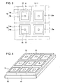
- Fig. 3 is a schematic plan view illustrating arrangement of each configuration in a pixel of an Example 1
- Fig. 4 is a schematic perspective view illustrating a configuration of a base portion of the Example 1.
- a second concave portion 91 of a tetragon (square) is arranged in a nearly center part of a pixel 20a in a planar fashion.
- a first concave portion 90 having a greater depth than that of the second concave 91 is arranged to surround the second concave portion 91, spaced apart from the second concave portion 90.
- An outer shape of the first concave portion 90 is also a tetragon (square).
- the first concave portion 90 is about 5 ⁇ m in width, and is about 15 ⁇ m in depth corresponding to the height of the base portion 11.
- the second concave portion 91 is about 5 ⁇ m in width (length of a side of square) and is about 5 ⁇ m in depth, which is less than that of the first concave portion 90.
- pixels 20a each having the first concave portion 90 and the second concave portion 91 are arranged on the circuit board 10 in a matrix pattern.
- a reflection plate 13 provided on the base portion 11 is disposed between first electrodes 19a (first concave portions 90) of adjacent pixels 20a and between a first electrode 19a (first concave portion 90) and a second electrode 19b (second concave portion 91) in each pixel 20a.
- first concave portion 90 and the second concave portion 91 having different depths may be reversed. That is, a first concave portion 90 may be disposed at a center side of the pixel 20a and the second concave portion 91 may be arranged to surround the first concave portion 90.
- black particles 61 as electrophoretic particles may be evenly received at an aperture of the first concave portion 90 or the second concave portion 91 or the received black particles 61 may be evenly discharged to the dispersion liquid 60 in the same manner.
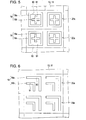
- Fig. 5 is a schematic plan view illustrating arrangement of each configuration in a pixel according to an Example 2.
- the second concave portion 91 has a'+' (plus) shape.
- the second concave portion 91 is about 5 ⁇ m in width and in depth identical with those of the Example 1.
- a volume of an aperture of the second concave portion 91 formed on the base portion 11 may be increased in comparison with the Example 1. That is, the black particles 61 may be rapidly received in the second concave portion 91 or the received black particles 61 may be discharged to the dispersion liquid 60 equally and rapidly. That is, response speed on an outer appearance may be increased in comparison with the Example 1.
- first concave portion 90 and the second concave portion 91 having different depths may be exchanged with each other. That is, a first concave portion 90 of a '+' (plus) shape may be disposed at a center side of the pixel 20a and the second concave portion 91 may be arranged to surround the first concave portion 90.
- Fig. 6 is a schematic plan view illustrating arrangement of each configuration in a pixel according to an Example 3. Arrangements of a first electrode 19a (first concave portion 90) and a second electrode 19b (second concave portion 91) are not limited to a case where one electrode surrounds another electrode as in the Example 1 or 2. For example, as shown in Fig.
- Example 3 a first concave portion 90 (first electrode 19a)is provided perpendicularly bent along and adjacent to two sides of each of a plurality of pixels 20a, which are arranged in a matrix pattern, and a second concave portion 91 (second electrode 19b) is provided to be similarly and perpendicularly bent at an inner side in comparison with the first concave portion 90 and to be spaced apart from the first concave portion 90 (first electrode 19a) by a predetermined distance.
- a planar distance between the first concave portion 90 (first electrode 19a) and the second concave portion 91 (second electrode 19b) is constant, and a part may be provided in adjacent pixels 20a in which a planar distance between the first concave portion 90 (first electrode 19a) and the second concave portion 91 (second electrode 19b) is constant. That is, the black particles 61 may be received at an aperture between the first concave portion 90 and the second concave portion 91 to easily perform white display, and the received black particles 61 may be discharged and drawn to the opposite electrode 21 side to perform black display.
- Example 3 in the same manner as in the Example 1, the arrangements of the first concave portion 90 and the second concave portion 91 having different depths may be exchanged with each other. That is, a second concave portion 91 may be provided at a location along adjacent sides of the pixel 20a, and thus a first concave portion 90 may be arranged at an inner side of the second concave portion 91.
- the electrophoretic display 1 includes a controller 110, a scanning line driving circuit 120, and a data line driving circuit 130. Moreover, the controller 110, the scanning line driving circuit 120, and the data line driving circuit 130 construct a driver according to the aspect of the invention.
- the controller 110, the scanning line driving circuit 120, and the data line driving circuit 130 are provided around a display region 10a on the circuit board 10.
- m scan lines 40 namely, scan lines Y1, Y2,..., Ym
- n data lines 50 (X1, X2,..., Xn) are provided intersecting each other on the display region 10a on the circuit board 10.
- the m scan lines 40 extend in rows (namely, X direction) and the n data lines 50 extend in columns (namely, Y direction).
- Pixels 20a are arranged corresponding to the intersections between the m scan lines 40 and the n data lines 50.
- the controller 110 controls operations of the scanning line driving circuit 120 and the data line driving circuit 130. Specifically, for example, the controller 110 supplies a timing signal such as a clock signal or a start pulse to respective circuits or supplies an image signal based on image information to the pixel electrode 19.
- a timing signal such as a clock signal or a start pulse
- the scanning line driving circuit 120 sequentially supplies a scan signal to the scan lines 40 (Y1, Y2,..., Ym) in a pulse form based on the timing signal provided from the controller 110.
- the data line driving circuit 130 supplies an image signal to the data lines 50 (X1, X2,..., Xn) based on the timing signal provided from the controller 110.
- the image signal is at a binary level composed of high electric potential level (referred to as “high level” hereinafter, e.g., +15V) or low electric potential level (referred to as “low level” hereinafter, e.g., -15V).
- the foregoing pixel electrode 19 and a transistor 72 are provided in the pixel 20a.
- a gate of the transistor 72 is electrically connected to the scan lines 40, a source thereof is electrically connected to the data lines 50, and a drain thereof is electrically connected to the pixel electrode 19.
- a scan signal is supplied from the scanning line driving circuit 120 to the scan lines 40 to turn-on the transistor 72, and the pixel electrode 19 and the data lines 50 are electrically connected to each other. According to this, an image signal is supplied from the data lines 50 to the pixel electrode 19.
- Fig. 8 is a schematic cross-sectional view illustrating an arrangement of respective electric potentials of a pixel electrode 19 and an opposite electrode 21 and arrangement of black particles 61 in a pattern fashion when an electrophoretic display 1 displays white on respective pixels 20a.
- Fig. 9 is a schematic cross-sectional view illustrating respective electric potentials of a pixel electrode 19 and an opposite electrode 21 and arrangement of black particles 61 in a pattern fashion when an electrophoretic display 1 displays black on respective pixels 20a. Further, a configuration of a pixel 20a of the Example 1 will be described by way of example.
- an electric potential level of the opposite electrode 21 is fixed, for example, at level 0 (GND level). If an image signal of low level (L) is supplied to a first electrode 19a of a pixel electrode 19, a plurality of black particles 61 normally charged is moved to a first electrode 19a side and received in the first concave portion 90 by an electric force (coulomb force) caused from the electric field between a first electrode 19a of the pixel electrode 19 and the opposite electrode 21. Accordingly, most or all of the black particles 61 overlapping the reflection plate 13 are absent when viewed in a plan view on the circuit board 10 (refer to Fig. 1 and Fig. 2 ), and light may be surely reflected from the reflection plate 13. As a result, white may be displayed on each pixel 20a.
- a signal of high level (H) is supplied to the first electrode 19a of the pixel electrode 19
- a plurality of black particles 61 normally discharged are moved to the opposite electrode 21 side by an electric force due to the electric field between the first electrode 19a and the opposite electrode 21, and arranged on the opposite substrate 20, and incident light is absorbed by the black particles 61. Accordingly, black may be displayed.
- first electrode 19a of the pixel electrode 19 is described, a second electrode 19b of the pixel electrode 19 may be controlled in the same manner as the first electrode 19a.
- the black particles 61 may be all received in the first concave portion 90 and/or the second concave portion 91 such that white display of high quality can be performed.
- a case where the second electrode 19b is controlled in a different manner from that of the first electrode 19a may be considered.
- an electric potential having the same polarity as that of the first electrode 19a may be delayed and applied to the second electrode 19b.
- this control for example, when an electric potential is initially applied to the first electrode 19a, a part of the black particles 61 is received in the first concave portion 90.
- the electric potential is next applied to the second electrode 19b, the remaining black particles 61 may be received in the second concave portion 91.
- a volume of the first concave portion 90 is designed to be larger than that of the second concave portion 91, thereby performing initial reception at high speed and increasing visibility.
- the second electrode 19b is formed in a second concave portion 91 of the base portion 11, and is closer to the opposite electrode 21 in comparison with the first electrode 19a. Accordingly, the black particles 61 may be received in the second concave portion 91 reliably in comparison with a case where the second electrode 19b is formed on the circuit board 10. Therefore, it has effect in that white display may be more rapidly and clearly performed in comparison with a case where only the first concave portion 90 is provided.
- a concentration of particles in the dispersion liquid 60 may be reduced in comparison with a case where black particles 61 and white particles are dispersed in the dispersion liquid 60, and moving speed of the black particles 61 in the dispersion liquid 60 (in other words, response speed of a black particle 61 to a voltage applied between the first electrode 19a and the opposite electrode 21) may be increased. As a result, display speed switching display may be increased.
- the white since light is reflected from the reflection plate 13 to display white, the white may be clearly displayed on the display region 10a.
- the black particles 61 are received in the first concave portion 90 and the second concave portion 91 between adjacent pixels 20a, since the first concave portion 90 and the second concave portion 91 are about 5 ⁇ m in width, the reflection plate 13 scatters the light in a plurality of directions such that it is difficult to recognize presence of the first concave portion 90 and the second concave portion 91. This does not adversely affect (e.g., brightness or deterioration in contrast) display of a color (namely, black) of the black particles 61 received in an aperture between the first concave portion 90 and the second concave portion 91 substantially or at all.
- a color namely, black
- the first concave portion 90 and the second concave portion 91 are preferably less than or equal to 5 ⁇ m in width.
- widths or depths of the first concave portion 90 and the second concave portion 91 are adjusted such that a total volume of black particles 61 corresponding to each pixel 20a is smaller than that of the first concave portion 90 and the second concave portion 91. Accordingly, a case where a plurality of black particles 61 cannot be received can be avoided when displaying white in each pixel 20a. That is, a plurality of black particles 61 may be certainly received, and white display may be clearly performed.
- high-quality display may be performed.
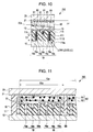
- Fig. 10 is a view illustrating a configuration of a pixel in an electrophoretic display according to a second embodiment.
- the same reference numerals in Fig. 10 are used as throughout the drawings to refer to the same or like parts in the first embodiment, and thus a description thereof is appropriately omitted.
- an electrophoretic display 200 according to the second embodiment has a side portion 19c of the first electrode 19a besides the first electrode 19a of the pixel electrode 19. Except for the foregoing point, a construction of the second embodiment is substantially the same as that of the electrophoretic display 1 according to the first embodiment.
- the base portion 11 b has a cut portion 111 formed in which a part of a side of a first concave portion 90 of a corresponding base portion 11 b is cut.
- the cut portion 111 is cut from a lower surface 11 bu of the base portion 11 b towards an upper side (dispersion liquid 60 side or opposite substrate 20 side) of the first concave portion 90 by a length D1.
- the cut portion 111 has the side portion 19c which is an electrode provided along a side 111S in the cut portion 111 of the base portion 11b.
- a reflection plate 13 is provided on the base portion 11b.
- FIG. 10 illustrates that a plurality of black particles 61 are received in the first concave portion 90 and the second concave portion 91 as a signal of low level (L) is supplied to the first electrode 19a, a second electrode 19b, and a side portion 19c of the first electrode 19a.
- L low level
- the first electrode 19a and the side portion 19c of the first electrode 19a may draw the black particles 61 dispersed in the dispersion liquid 60 rapidly and certainly.
- Fig. 11 is a cross-sectional view illustrating a configuration of an electrophoretic display according to a third embodiment.
- the same reference numerals in Fig. 11 are used as throughout the drawings to refer to the same or like parts in the first embodiment, and thus a description thereof is appropriately omitted.
- an electrophoretic display 300 according to the third embodiment has a partition 80. Except for the foregoing point, a construction of the third embodiment is substantially the same as that of the electrophoretic display 1 according to the first embodiment.
- the partition 80 is provided between a circuit board 10 and an opposite substrate 20 to compartmentalise a display region 10a (in other words, electrophoretic layer 60) into a plurality of regions 80a.
- the partition 80 has reticular pattern when viewed in plan.
- the partition 80 is provided between the circuit board 10 and the opposite substrate 20, for example, strength of pressure applied to the circuit board 10 side or the opposite substrate 20 side may be increased.
- a plurality of pixel electrodes 19 are included in each of a plurality of regions 80a formed by the partition 80 (in other words, a plurality of pixels 20a are included). Since a region of the display region 10a in which the partition 80 is arranged (in other words, region not contributing to display) is shallower than the corresponding region in the first embodiment, where the partition 80 is not provided, bright and high contrast display may be performed.
- Fig. 12 is a perspective view illustrating a configuration of an electronic paper as an electronic device.
- the electronic paper 1400 has the electrophoretic display according to the foregoing embodiment as a display unit 1401.
- the electronic paper 1400 has flexibility, and includes a body 1402 configured by a rewritable sheet having the same bendability and texture as those of the related art.
- Fig. 13 is a perspective view illustrating a configuration of an electronic notebook as an electronic device.
- the electronic notebook 1500 is configured by tying a plurality of electronic papers 1400 shown in Fig. 12 and inserting the tied electronic papers 1400 in a cover 1501.
- the cover 1501 has a display data input means (not shown) for receiving input of display data provided from, for example, an external device. According to this, according to the display data, in a state that the electronic papers 1400 are tied, display content may be changed or updated.
- the embodiments of the present disclosure are not limited to the first to third embodiments described above, and various modifications are possible within a scope of the present disclosure.
- An electrophoretic display involving such modifications and an electronic device with the same may be included in a technical scope of the invention.
- a planar shape of the pixel 20a in other words, a planar shape of the first concave portion 90 (first electrode 19a) or the second concave portion 91 (second electrode 19b) is not limited to a square.
- the planar shape of the pixel 20a may be a polygon or circle.
Landscapes
- Physics & Mathematics (AREA)
- Nonlinear Science (AREA)
- General Physics & Mathematics (AREA)
- Optics & Photonics (AREA)
- Engineering & Computer Science (AREA)
- Electrochemistry (AREA)
- Molecular Biology (AREA)
- Chemical Kinetics & Catalysis (AREA)
- Chemical & Material Sciences (AREA)
- Life Sciences & Earth Sciences (AREA)
- Health & Medical Sciences (AREA)
- Computer Hardware Design (AREA)
- Theoretical Computer Science (AREA)
- Electrochromic Elements, Electrophoresis, Or Variable Reflection Or Absorption Elements (AREA)
- Devices For Indicating Variable Information By Combining Individual Elements (AREA)
Applications Claiming Priority (1)
| Application Number | Priority Date | Filing Date | Title |
|---|---|---|---|
| JP2011127022A JP2012252294A (ja) | 2011-06-07 | 2011-06-07 | 電気泳動表示装置および電子機器 |
Publications (2)
| Publication Number | Publication Date |
|---|---|
| EP2533098A1 EP2533098A1 (en) | 2012-12-12 |
| EP2533098B1 true EP2533098B1 (en) | 2013-11-13 |
Family
ID=46298238
Family Applications (1)
| Application Number | Title | Priority Date | Filing Date |
|---|---|---|---|
| EP12168388.2A Active EP2533098B1 (en) | 2011-06-07 | 2012-05-16 | Electrophoretic display and electronic device |
Country Status (6)
Families Citing this family (5)
| Publication number | Priority date | Publication date | Assignee | Title |
|---|---|---|---|---|
| CN104298011A (zh) | 2014-09-05 | 2015-01-21 | 深圳市华星光电技术有限公司 | 一种掩模板及使用掩模板制作光阻间隔物的方法 |
| EP3250962B1 (en) | 2014-12-02 | 2019-08-28 | Tim R. Koch | Two particle electrophoretic laminate for use with smart windows with reduced diffraction |
| CN107290914B (zh) * | 2016-04-01 | 2022-09-09 | 上海伯乐电子有限公司 | 电子纸显示模组及其制备方法、电子纸显示装置 |
| CN106681063B (zh) * | 2016-10-28 | 2019-08-16 | 京东方科技集团股份有限公司 | 显示面板及其制作方法、显示装置 |
| TW202516256A (zh) | 2019-02-27 | 2025-04-16 | 加拿大商哈利恩顯示股份有限公司 | 製造顯示組件的方法 |
Family Cites Families (14)
| Publication number | Priority date | Publication date | Assignee | Title |
|---|---|---|---|---|
| JPH02165127A (ja) * | 1988-12-20 | 1990-06-26 | Toyota Motor Corp | 立体的電気泳動型表示素子 |
| JP3610300B2 (ja) * | 1999-11-08 | 2005-01-12 | キヤノン株式会社 | 電気泳動表示装置およびその駆動方法 |
| JP2003005226A (ja) | 2001-06-26 | 2003-01-08 | Canon Inc | 電気泳動表示装置 |
| JP3715906B2 (ja) | 2001-06-26 | 2005-11-16 | キヤノン株式会社 | 電気泳動表示装置、及び該電気泳動表示装置の駆動方法 |
| JP3927084B2 (ja) * | 2001-07-13 | 2007-06-06 | セイコーエプソン株式会社 | 液晶表示パネル用カラーフィルタ基板 |
| JP4416380B2 (ja) * | 2002-06-14 | 2010-02-17 | キヤノン株式会社 | 電気泳動表示装置およびその駆動方法 |
| JP4806220B2 (ja) * | 2005-07-08 | 2011-11-02 | 株式会社 日立ディスプレイズ | 画像表示装置 |
| JP4720547B2 (ja) * | 2006-03-07 | 2011-07-13 | 株式会社日立製作所 | 画像表示装置 |
| JP4816245B2 (ja) * | 2006-05-19 | 2011-11-16 | 株式会社日立製作所 | 電気泳動表示装置 |
| US20080150840A1 (en) * | 2006-12-20 | 2008-06-26 | Kang Kyung-Won | Plasma display panel and driving method thereof |
| JP2010091908A (ja) | 2008-10-10 | 2010-04-22 | Konica Minolta Business Technologies Inc | 画像表示装置 |
| JP2010197649A (ja) * | 2009-02-25 | 2010-09-09 | Fuji Xerox Co Ltd | 画像表示媒体および画像表示装置 |
| JP5471497B2 (ja) * | 2009-07-30 | 2014-04-16 | セイコーエプソン株式会社 | 電気泳動表示体、電気泳動表示装置および電子機器 |
| JP5594069B2 (ja) * | 2010-11-05 | 2014-09-24 | セイコーエプソン株式会社 | 電気泳動表示装置及び電子機器 |
-
2011
- 2011-06-07 JP JP2011127022A patent/JP2012252294A/ja not_active Withdrawn
-
2012
- 2012-05-16 EP EP12168388.2A patent/EP2533098B1/en active Active
- 2012-05-23 US US13/478,477 patent/US20120314274A1/en not_active Abandoned
- 2012-06-04 KR KR1020120059664A patent/KR20120135872A/ko not_active Withdrawn
- 2012-06-04 TW TW101120000A patent/TW201250360A/zh unknown
- 2012-06-05 CN CN2012101826791A patent/CN102819161A/zh active Pending
Also Published As
| Publication number | Publication date |
|---|---|
| JP2012252294A (ja) | 2012-12-20 |
| CN102819161A (zh) | 2012-12-12 |
| KR20120135872A (ko) | 2012-12-17 |
| US20120314274A1 (en) | 2012-12-13 |
| EP2533098A1 (en) | 2012-12-12 |
| TW201250360A (en) | 2012-12-16 |
Similar Documents
| Publication | Publication Date | Title |
|---|---|---|
| US8422117B2 (en) | Electrophoretic display and electronics device | |
| JP4449974B2 (ja) | 電気光学パネル、電気光学装置、及び電気光学装置の駆動方法 | |
| JP4260482B2 (ja) | 電気泳動ディスプレイデバイス | |
| EP2533098B1 (en) | Electrophoretic display and electronic device | |
| EP3853662B1 (en) | Electrowetting on dielectric device with hexagonal and triangular electrodes | |
| US20120134009A1 (en) | Multi-color electrophoretic displays | |
| JP5286738B2 (ja) | 電気泳動表示シート、電気泳動表示装置および電子機器 | |
| US7277219B2 (en) | Particle movement-type display device and particle movement-type display apparatus | |
| US20110285756A1 (en) | Electrophoretic display device, driving method therefor, and electronic apparatus | |
| JP2011237771A (ja) | 電気泳動表示装置および電子機器 | |
| US20230205041A1 (en) | Optical path control device and display device including the same | |
| JP2012181451A (ja) | 電気泳動表示装置およびその駆動方法、電子機器 | |
| US8547324B2 (en) | Electrophoretic display sheet, electrophoretic display apparatus, and electronic device | |
| CN105372884A (zh) | 液晶显示面板及应用该液晶显示面板的电子装置 | |
| US8730561B2 (en) | Electrophoretic display device and driving method thereof | |
| US8724212B2 (en) | Electrophoretic display device and electronic apparatus | |
| KR20070071037A (ko) | 전기영동 표시장치 및 그 구동방법 | |
| US20250013116A1 (en) | Electronic paper display and driving method thereof | |
| JP2021012283A (ja) | 視野角制御パネル及び表示装置 | |
| KR100907272B1 (ko) | 전기영동 표시장치 | |
| JP2009265270A (ja) | 電気光学表示装置 | |
| KR101098544B1 (ko) | 단일입자를 이용한 전자종이 디스플레이 장치 | |
| CN118393793A (zh) | 透反式显示装置及驱动方法 | |
| KR101618232B1 (ko) | 잉크필름, 전기영동 표시 장치 및 이들의 제조방법 | |
| JP2012093385A (ja) | 表示シート、表示装置および電子機器 |
Legal Events
| Date | Code | Title | Description |
|---|---|---|---|
| PUAI | Public reference made under article 153(3) epc to a published international application that has entered the european phase |
Free format text: ORIGINAL CODE: 0009012 |
|
| AK | Designated contracting states |
Kind code of ref document: A1 Designated state(s): AL AT BE BG CH CY CZ DE DK EE ES FI FR GB GR HR HU IE IS IT LI LT LU LV MC MK MT NL NO PL PT RO RS SE SI SK SM TR |
|
| AX | Request for extension of the european patent |
Extension state: BA ME |
|
| 17P | Request for examination filed |
Effective date: 20130612 |
|
| RBV | Designated contracting states (corrected) |
Designated state(s): AL AT BE BG CH CY CZ DE DK EE ES FI FR GB GR HR HU IE IS IT LI LT LU LV MC MK MT NL NO PL PT RO RS SE SI SK SM TR |
|
| GRAP | Despatch of communication of intention to grant a patent |
Free format text: ORIGINAL CODE: EPIDOSNIGR1 |
|
| INTG | Intention to grant announced |
Effective date: 20130806 |
|
| GRAS | Grant fee paid |
Free format text: ORIGINAL CODE: EPIDOSNIGR3 |
|
| GRAA | (expected) grant |
Free format text: ORIGINAL CODE: 0009210 |
|
| AK | Designated contracting states |
Kind code of ref document: B1 Designated state(s): AL AT BE BG CH CY CZ DE DK EE ES FI FR GB GR HR HU IE IS IT LI LT LU LV MC MK MT NL NO PL PT RO RS SE SI SK SM TR |
|
| REG | Reference to a national code |
Ref country code: GB Ref legal event code: FG4D |
|
| REG | Reference to a national code |
Ref country code: CH Ref legal event code: EP |
|
| REG | Reference to a national code |
Ref country code: AT Ref legal event code: REF Ref document number: 640807 Country of ref document: AT Kind code of ref document: T Effective date: 20131215 |
|
| REG | Reference to a national code |
Ref country code: IE Ref legal event code: FG4D |
|
| REG | Reference to a national code |
Ref country code: DE Ref legal event code: R096 Ref document number: 602012000499 Country of ref document: DE Effective date: 20140109 |
|
| REG | Reference to a national code |
Ref country code: NL Ref legal event code: VDEP Effective date: 20131113 |
|
| REG | Reference to a national code |
Ref country code: AT Ref legal event code: MK05 Ref document number: 640807 Country of ref document: AT Kind code of ref document: T Effective date: 20131113 |
|
| REG | Reference to a national code |
Ref country code: LT Ref legal event code: MG4D |
|
| PG25 | Lapsed in a contracting state [announced via postgrant information from national office to epo] |
Ref country code: SE Free format text: LAPSE BECAUSE OF FAILURE TO SUBMIT A TRANSLATION OF THE DESCRIPTION OR TO PAY THE FEE WITHIN THE PRESCRIBED TIME-LIMIT Effective date: 20131113 Ref country code: HR Free format text: LAPSE BECAUSE OF FAILURE TO SUBMIT A TRANSLATION OF THE DESCRIPTION OR TO PAY THE FEE WITHIN THE PRESCRIBED TIME-LIMIT Effective date: 20131113 Ref country code: FI Free format text: LAPSE BECAUSE OF FAILURE TO SUBMIT A TRANSLATION OF THE DESCRIPTION OR TO PAY THE FEE WITHIN THE PRESCRIBED TIME-LIMIT Effective date: 20131113 Ref country code: IS Free format text: LAPSE BECAUSE OF FAILURE TO SUBMIT A TRANSLATION OF THE DESCRIPTION OR TO PAY THE FEE WITHIN THE PRESCRIBED TIME-LIMIT Effective date: 20140313 Ref country code: NO Free format text: LAPSE BECAUSE OF FAILURE TO SUBMIT A TRANSLATION OF THE DESCRIPTION OR TO PAY THE FEE WITHIN THE PRESCRIBED TIME-LIMIT Effective date: 20140213 Ref country code: NL Free format text: LAPSE BECAUSE OF FAILURE TO SUBMIT A TRANSLATION OF THE DESCRIPTION OR TO PAY THE FEE WITHIN THE PRESCRIBED TIME-LIMIT Effective date: 20131113 Ref country code: LT Free format text: LAPSE BECAUSE OF FAILURE TO SUBMIT A TRANSLATION OF THE DESCRIPTION OR TO PAY THE FEE WITHIN THE PRESCRIBED TIME-LIMIT Effective date: 20131113 |
|
| PG25 | Lapsed in a contracting state [announced via postgrant information from national office to epo] |
Ref country code: CY Free format text: LAPSE BECAUSE OF FAILURE TO SUBMIT A TRANSLATION OF THE DESCRIPTION OR TO PAY THE FEE WITHIN THE PRESCRIBED TIME-LIMIT Effective date: 20131113 Ref country code: RS Free format text: LAPSE BECAUSE OF FAILURE TO SUBMIT A TRANSLATION OF THE DESCRIPTION OR TO PAY THE FEE WITHIN THE PRESCRIBED TIME-LIMIT Effective date: 20131113 Ref country code: BE Free format text: LAPSE BECAUSE OF FAILURE TO SUBMIT A TRANSLATION OF THE DESCRIPTION OR TO PAY THE FEE WITHIN THE PRESCRIBED TIME-LIMIT Effective date: 20131113 Ref country code: ES Free format text: LAPSE BECAUSE OF FAILURE TO SUBMIT A TRANSLATION OF THE DESCRIPTION OR TO PAY THE FEE WITHIN THE PRESCRIBED TIME-LIMIT Effective date: 20131113 Ref country code: AT Free format text: LAPSE BECAUSE OF FAILURE TO SUBMIT A TRANSLATION OF THE DESCRIPTION OR TO PAY THE FEE WITHIN THE PRESCRIBED TIME-LIMIT Effective date: 20131113 Ref country code: LV Free format text: LAPSE BECAUSE OF FAILURE TO SUBMIT A TRANSLATION OF THE DESCRIPTION OR TO PAY THE FEE WITHIN THE PRESCRIBED TIME-LIMIT Effective date: 20131113 |
|
| PG25 | Lapsed in a contracting state [announced via postgrant information from national office to epo] |
Ref country code: PT Free format text: LAPSE BECAUSE OF FAILURE TO SUBMIT A TRANSLATION OF THE DESCRIPTION OR TO PAY THE FEE WITHIN THE PRESCRIBED TIME-LIMIT Effective date: 20140313 |
|
| PG25 | Lapsed in a contracting state [announced via postgrant information from national office to epo] |
Ref country code: EE Free format text: LAPSE BECAUSE OF FAILURE TO SUBMIT A TRANSLATION OF THE DESCRIPTION OR TO PAY THE FEE WITHIN THE PRESCRIBED TIME-LIMIT Effective date: 20131113 |
|
| REG | Reference to a national code |
Ref country code: DE Ref legal event code: R097 Ref document number: 602012000499 Country of ref document: DE |
|
| PG25 | Lapsed in a contracting state [announced via postgrant information from national office to epo] |
Ref country code: SK Free format text: LAPSE BECAUSE OF FAILURE TO SUBMIT A TRANSLATION OF THE DESCRIPTION OR TO PAY THE FEE WITHIN THE PRESCRIBED TIME-LIMIT Effective date: 20131113 Ref country code: PL Free format text: LAPSE BECAUSE OF FAILURE TO SUBMIT A TRANSLATION OF THE DESCRIPTION OR TO PAY THE FEE WITHIN THE PRESCRIBED TIME-LIMIT Effective date: 20131113 Ref country code: CZ Free format text: LAPSE BECAUSE OF FAILURE TO SUBMIT A TRANSLATION OF THE DESCRIPTION OR TO PAY THE FEE WITHIN THE PRESCRIBED TIME-LIMIT Effective date: 20131113 |
|
| PLBE | No opposition filed within time limit |
Free format text: ORIGINAL CODE: 0009261 |
|
| STAA | Information on the status of an ep patent application or granted ep patent |
Free format text: STATUS: NO OPPOSITION FILED WITHIN TIME LIMIT |
|
| PG25 | Lapsed in a contracting state [announced via postgrant information from national office to epo] |
Ref country code: DK Free format text: LAPSE BECAUSE OF FAILURE TO SUBMIT A TRANSLATION OF THE DESCRIPTION OR TO PAY THE FEE WITHIN THE PRESCRIBED TIME-LIMIT Effective date: 20131113 |
|
| 26N | No opposition filed |
Effective date: 20140814 |
|
| REG | Reference to a national code |
Ref country code: DE Ref legal event code: R097 Ref document number: 602012000499 Country of ref document: DE Effective date: 20140814 |
|
| PG25 | Lapsed in a contracting state [announced via postgrant information from national office to epo] |
Ref country code: LU Free format text: LAPSE BECAUSE OF FAILURE TO SUBMIT A TRANSLATION OF THE DESCRIPTION OR TO PAY THE FEE WITHIN THE PRESCRIBED TIME-LIMIT Effective date: 20140516 |
|
| PG25 | Lapsed in a contracting state [announced via postgrant information from national office to epo] |
Ref country code: MC Free format text: LAPSE BECAUSE OF FAILURE TO SUBMIT A TRANSLATION OF THE DESCRIPTION OR TO PAY THE FEE WITHIN THE PRESCRIBED TIME-LIMIT Effective date: 20131113 |
|
| REG | Reference to a national code |
Ref country code: IE Ref legal event code: MM4A |
|
| PG25 | Lapsed in a contracting state [announced via postgrant information from national office to epo] |
Ref country code: SI Free format text: LAPSE BECAUSE OF FAILURE TO SUBMIT A TRANSLATION OF THE DESCRIPTION OR TO PAY THE FEE WITHIN THE PRESCRIBED TIME-LIMIT Effective date: 20131113 |
|
| PG25 | Lapsed in a contracting state [announced via postgrant information from national office to epo] |
Ref country code: IE Free format text: LAPSE BECAUSE OF NON-PAYMENT OF DUE FEES Effective date: 20140516 Ref country code: IT Free format text: LAPSE BECAUSE OF FAILURE TO SUBMIT A TRANSLATION OF THE DESCRIPTION OR TO PAY THE FEE WITHIN THE PRESCRIBED TIME-LIMIT Effective date: 20131113 |
|
| REG | Reference to a national code |
Ref country code: CH Ref legal event code: PL |
|
| PG25 | Lapsed in a contracting state [announced via postgrant information from national office to epo] |
Ref country code: CH Free format text: LAPSE BECAUSE OF NON-PAYMENT OF DUE FEES Effective date: 20150531 Ref country code: LI Free format text: LAPSE BECAUSE OF NON-PAYMENT OF DUE FEES Effective date: 20150531 |
|
| PG25 | Lapsed in a contracting state [announced via postgrant information from national office to epo] |
Ref country code: MT Free format text: LAPSE BECAUSE OF FAILURE TO SUBMIT A TRANSLATION OF THE DESCRIPTION OR TO PAY THE FEE WITHIN THE PRESCRIBED TIME-LIMIT Effective date: 20131113 |
|
| REG | Reference to a national code |
Ref country code: FR Ref legal event code: PLFP Year of fee payment: 5 |
|
| PG25 | Lapsed in a contracting state [announced via postgrant information from national office to epo] |
Ref country code: SM Free format text: LAPSE BECAUSE OF FAILURE TO SUBMIT A TRANSLATION OF THE DESCRIPTION OR TO PAY THE FEE WITHIN THE PRESCRIBED TIME-LIMIT Effective date: 20131113 |
|
| PG25 | Lapsed in a contracting state [announced via postgrant information from national office to epo] |
Ref country code: RO Free format text: LAPSE BECAUSE OF FAILURE TO SUBMIT A TRANSLATION OF THE DESCRIPTION OR TO PAY THE FEE WITHIN THE PRESCRIBED TIME-LIMIT Effective date: 20131113 |
|
| PG25 | Lapsed in a contracting state [announced via postgrant information from national office to epo] |
Ref country code: BG Free format text: LAPSE BECAUSE OF FAILURE TO SUBMIT A TRANSLATION OF THE DESCRIPTION OR TO PAY THE FEE WITHIN THE PRESCRIBED TIME-LIMIT Effective date: 20131113 Ref country code: GR Free format text: LAPSE BECAUSE OF FAILURE TO SUBMIT A TRANSLATION OF THE DESCRIPTION OR TO PAY THE FEE WITHIN THE PRESCRIBED TIME-LIMIT Effective date: 20140214 |
|
| PG25 | Lapsed in a contracting state [announced via postgrant information from national office to epo] |
Ref country code: HU Free format text: LAPSE BECAUSE OF FAILURE TO SUBMIT A TRANSLATION OF THE DESCRIPTION OR TO PAY THE FEE WITHIN THE PRESCRIBED TIME-LIMIT; INVALID AB INITIO Effective date: 20120516 Ref country code: TR Free format text: LAPSE BECAUSE OF FAILURE TO SUBMIT A TRANSLATION OF THE DESCRIPTION OR TO PAY THE FEE WITHIN THE PRESCRIBED TIME-LIMIT Effective date: 20131113 |
|
| REG | Reference to a national code |
Ref country code: FR Ref legal event code: PLFP Year of fee payment: 6 |
|
| REG | Reference to a national code |
Ref country code: FR Ref legal event code: PLFP Year of fee payment: 7 |
|
| PG25 | Lapsed in a contracting state [announced via postgrant information from national office to epo] |
Ref country code: MK Free format text: LAPSE BECAUSE OF FAILURE TO SUBMIT A TRANSLATION OF THE DESCRIPTION OR TO PAY THE FEE WITHIN THE PRESCRIBED TIME-LIMIT Effective date: 20131113 |
|
| PG25 | Lapsed in a contracting state [announced via postgrant information from national office to epo] |
Ref country code: AL Free format text: LAPSE BECAUSE OF FAILURE TO SUBMIT A TRANSLATION OF THE DESCRIPTION OR TO PAY THE FEE WITHIN THE PRESCRIBED TIME-LIMIT Effective date: 20131113 |
|
| PGFP | Annual fee paid to national office [announced via postgrant information from national office to epo] |
Ref country code: DE Payment date: 20250423 Year of fee payment: 14 |
|
| PGFP | Annual fee paid to national office [announced via postgrant information from national office to epo] |
Ref country code: GB Payment date: 20250423 Year of fee payment: 14 |
|
| PGFP | Annual fee paid to national office [announced via postgrant information from national office to epo] |
Ref country code: FR Payment date: 20250423 Year of fee payment: 14 |