EP2531350B1 - Nano-oxid-verfahren zum bonden einer kupfer-/kupferlegierung und harz - Google Patents
Nano-oxid-verfahren zum bonden einer kupfer-/kupferlegierung und harz Download PDFInfo
- Publication number
- EP2531350B1 EP2531350B1 EP10844927.3A EP10844927A EP2531350B1 EP 2531350 B1 EP2531350 B1 EP 2531350B1 EP 10844927 A EP10844927 A EP 10844927A EP 2531350 B1 EP2531350 B1 EP 2531350B1
- Authority
- EP
- European Patent Office
- Prior art keywords
- copper
- oxide
- composition
- phosphate
- composition according
- Prior art date
- Legal status (The legal status is an assumption and is not a legal conclusion. Google has not performed a legal analysis and makes no representation as to the accuracy of the status listed.)
- Active
Links
Images

Classifications
-
- B—PERFORMING OPERATIONS; TRANSPORTING
- B32—LAYERED PRODUCTS
- B32B—LAYERED PRODUCTS, i.e. PRODUCTS BUILT-UP OF STRATA OF FLAT OR NON-FLAT, e.g. CELLULAR OR HONEYCOMB, FORM
- B32B7/00—Layered products characterised by the relation between layers; Layered products characterised by the relative orientation of features between layers, or by the relative values of a measurable parameter between layers, i.e. products comprising layers having different physical, chemical or physicochemical properties; Layered products characterised by the interconnection of layers
- B32B7/04—Interconnection of layers
- B32B7/12—Interconnection of layers using interposed adhesives or interposed materials with bonding properties
-
- B—PERFORMING OPERATIONS; TRANSPORTING
- B32—LAYERED PRODUCTS
- B32B—LAYERED PRODUCTS, i.e. PRODUCTS BUILT-UP OF STRATA OF FLAT OR NON-FLAT, e.g. CELLULAR OR HONEYCOMB, FORM
- B32B15/00—Layered products comprising a layer of metal
- B32B15/04—Layered products comprising a layer of metal comprising metal as the main or only constituent of a layer, which is next to another layer of the same or of a different material
- B32B15/08—Layered products comprising a layer of metal comprising metal as the main or only constituent of a layer, which is next to another layer of the same or of a different material of synthetic resin
-
- B—PERFORMING OPERATIONS; TRANSPORTING
- B32—LAYERED PRODUCTS
- B32B—LAYERED PRODUCTS, i.e. PRODUCTS BUILT-UP OF STRATA OF FLAT OR NON-FLAT, e.g. CELLULAR OR HONEYCOMB, FORM
- B32B15/00—Layered products comprising a layer of metal
- B32B15/20—Layered products comprising a layer of metal comprising aluminium or copper
-
- B—PERFORMING OPERATIONS; TRANSPORTING
- B32—LAYERED PRODUCTS
- B32B—LAYERED PRODUCTS, i.e. PRODUCTS BUILT-UP OF STRATA OF FLAT OR NON-FLAT, e.g. CELLULAR OR HONEYCOMB, FORM
- B32B27/00—Layered products comprising a layer of synthetic resin
- B32B27/06—Layered products comprising a layer of synthetic resin as the main or only constituent of a layer, which is next to another layer of the same or of a different material
-
- B—PERFORMING OPERATIONS; TRANSPORTING
- B32—LAYERED PRODUCTS
- B32B—LAYERED PRODUCTS, i.e. PRODUCTS BUILT-UP OF STRATA OF FLAT OR NON-FLAT, e.g. CELLULAR OR HONEYCOMB, FORM
- B32B7/00—Layered products characterised by the relation between layers; Layered products characterised by the relative orientation of features between layers, or by the relative values of a measurable parameter between layers, i.e. products comprising layers having different physical, chemical or physicochemical properties; Layered products characterised by the interconnection of layers
- B32B7/04—Interconnection of layers
-
- C—CHEMISTRY; METALLURGY
- C23—COATING METALLIC MATERIAL; COATING MATERIAL WITH METALLIC MATERIAL; CHEMICAL SURFACE TREATMENT; DIFFUSION TREATMENT OF METALLIC MATERIAL; COATING BY VACUUM EVAPORATION, BY SPUTTERING, BY ION IMPLANTATION OR BY CHEMICAL VAPOUR DEPOSITION, IN GENERAL; INHIBITING CORROSION OF METALLIC MATERIAL OR INCRUSTATION IN GENERAL
- C23C—COATING METALLIC MATERIAL; COATING MATERIAL WITH METALLIC MATERIAL; SURFACE TREATMENT OF METALLIC MATERIAL BY DIFFUSION INTO THE SURFACE, BY CHEMICAL CONVERSION OR SUBSTITUTION; COATING BY VACUUM EVAPORATION, BY SPUTTERING, BY ION IMPLANTATION OR BY CHEMICAL VAPOUR DEPOSITION, IN GENERAL
- C23C22/00—Chemical surface treatment of metallic material by reaction of the surface with a reactive liquid, leaving reaction products of surface material in the coating, e.g. conversion coatings, passivation of metals
- C23C22/05—Chemical surface treatment of metallic material by reaction of the surface with a reactive liquid, leaving reaction products of surface material in the coating, e.g. conversion coatings, passivation of metals using aqueous solutions
- C23C22/60—Chemical surface treatment of metallic material by reaction of the surface with a reactive liquid, leaving reaction products of surface material in the coating, e.g. conversion coatings, passivation of metals using aqueous solutions using alkaline aqueous solutions with pH greater than 8
- C23C22/63—Treatment of copper or alloys based thereon
-
- C—CHEMISTRY; METALLURGY
- C23—COATING METALLIC MATERIAL; COATING MATERIAL WITH METALLIC MATERIAL; CHEMICAL SURFACE TREATMENT; DIFFUSION TREATMENT OF METALLIC MATERIAL; COATING BY VACUUM EVAPORATION, BY SPUTTERING, BY ION IMPLANTATION OR BY CHEMICAL VAPOUR DEPOSITION, IN GENERAL; INHIBITING CORROSION OF METALLIC MATERIAL OR INCRUSTATION IN GENERAL
- C23C—COATING METALLIC MATERIAL; COATING MATERIAL WITH METALLIC MATERIAL; SURFACE TREATMENT OF METALLIC MATERIAL BY DIFFUSION INTO THE SURFACE, BY CHEMICAL CONVERSION OR SUBSTITUTION; COATING BY VACUUM EVAPORATION, BY SPUTTERING, BY ION IMPLANTATION OR BY CHEMICAL VAPOUR DEPOSITION, IN GENERAL
- C23C22/00—Chemical surface treatment of metallic material by reaction of the surface with a reactive liquid, leaving reaction products of surface material in the coating, e.g. conversion coatings, passivation of metals
- C23C22/78—Pretreatment of the material to be coated
-
- C—CHEMISTRY; METALLURGY
- C23—COATING METALLIC MATERIAL; COATING MATERIAL WITH METALLIC MATERIAL; CHEMICAL SURFACE TREATMENT; DIFFUSION TREATMENT OF METALLIC MATERIAL; COATING BY VACUUM EVAPORATION, BY SPUTTERING, BY ION IMPLANTATION OR BY CHEMICAL VAPOUR DEPOSITION, IN GENERAL; INHIBITING CORROSION OF METALLIC MATERIAL OR INCRUSTATION IN GENERAL
- C23C—COATING METALLIC MATERIAL; COATING MATERIAL WITH METALLIC MATERIAL; SURFACE TREATMENT OF METALLIC MATERIAL BY DIFFUSION INTO THE SURFACE, BY CHEMICAL CONVERSION OR SUBSTITUTION; COATING BY VACUUM EVAPORATION, BY SPUTTERING, BY ION IMPLANTATION OR BY CHEMICAL VAPOUR DEPOSITION, IN GENERAL
- C23C22/00—Chemical surface treatment of metallic material by reaction of the surface with a reactive liquid, leaving reaction products of surface material in the coating, e.g. conversion coatings, passivation of metals
- C23C22/82—After-treatment
- C23C22/83—Chemical after-treatment
-
- H—ELECTRICITY
- H05—ELECTRIC TECHNIQUES NOT OTHERWISE PROVIDED FOR
- H05K—PRINTED CIRCUITS; CASINGS OR CONSTRUCTIONAL DETAILS OF ELECTRIC APPARATUS; MANUFACTURE OF ASSEMBLAGES OF ELECTRICAL COMPONENTS
- H05K3/00—Apparatus or processes for manufacturing printed circuits
- H05K3/38—Improvement of the adhesion between the insulating substrate and the metal
- H05K3/388—Improvement of the adhesion between the insulating substrate and the metal by the use of a metallic or inorganic thin film adhesion layer
-
- B—PERFORMING OPERATIONS; TRANSPORTING
- B32—LAYERED PRODUCTS
- B32B—LAYERED PRODUCTS, i.e. PRODUCTS BUILT-UP OF STRATA OF FLAT OR NON-FLAT, e.g. CELLULAR OR HONEYCOMB, FORM
- B32B2255/00—Coating on the layer surface
- B32B2255/06—Coating on the layer surface on metal layer
-
- B—PERFORMING OPERATIONS; TRANSPORTING
- B32—LAYERED PRODUCTS
- B32B—LAYERED PRODUCTS, i.e. PRODUCTS BUILT-UP OF STRATA OF FLAT OR NON-FLAT, e.g. CELLULAR OR HONEYCOMB, FORM
- B32B2255/00—Coating on the layer surface
- B32B2255/20—Inorganic coating
- B32B2255/205—Metallic coating
-
- B—PERFORMING OPERATIONS; TRANSPORTING
- B32—LAYERED PRODUCTS
- B32B—LAYERED PRODUCTS, i.e. PRODUCTS BUILT-UP OF STRATA OF FLAT OR NON-FLAT, e.g. CELLULAR OR HONEYCOMB, FORM
- B32B2255/00—Coating on the layer surface
- B32B2255/24—Organic non-macromolecular coating
-
- B—PERFORMING OPERATIONS; TRANSPORTING
- B32—LAYERED PRODUCTS
- B32B—LAYERED PRODUCTS, i.e. PRODUCTS BUILT-UP OF STRATA OF FLAT OR NON-FLAT, e.g. CELLULAR OR HONEYCOMB, FORM
- B32B2307/00—Properties of the layers or laminate
- B32B2307/50—Properties of the layers or laminate having particular mechanical properties
-
- B—PERFORMING OPERATIONS; TRANSPORTING
- B32—LAYERED PRODUCTS
- B32B—LAYERED PRODUCTS, i.e. PRODUCTS BUILT-UP OF STRATA OF FLAT OR NON-FLAT, e.g. CELLULAR OR HONEYCOMB, FORM
- B32B2307/00—Properties of the layers or laminate
- B32B2307/70—Other properties
- B32B2307/732—Dimensional properties
-
- B—PERFORMING OPERATIONS; TRANSPORTING
- B32—LAYERED PRODUCTS
- B32B—LAYERED PRODUCTS, i.e. PRODUCTS BUILT-UP OF STRATA OF FLAT OR NON-FLAT, e.g. CELLULAR OR HONEYCOMB, FORM
- B32B2457/00—Electrical equipment
- B32B2457/08—PCBs, i.e. printed circuit boards
-
- H—ELECTRICITY
- H05—ELECTRIC TECHNIQUES NOT OTHERWISE PROVIDED FOR
- H05K—PRINTED CIRCUITS; CASINGS OR CONSTRUCTIONAL DETAILS OF ELECTRIC APPARATUS; MANUFACTURE OF ASSEMBLAGES OF ELECTRICAL COMPONENTS
- H05K2203/00—Indexing scheme relating to apparatus or processes for manufacturing printed circuits covered by H05K3/00
- H05K2203/03—Metal processing
- H05K2203/0315—Oxidising metal
-
- H—ELECTRICITY
- H05—ELECTRIC TECHNIQUES NOT OTHERWISE PROVIDED FOR
- H05K—PRINTED CIRCUITS; CASINGS OR CONSTRUCTIONAL DETAILS OF ELECTRIC APPARATUS; MANUFACTURE OF ASSEMBLAGES OF ELECTRICAL COMPONENTS
- H05K3/00—Apparatus or processes for manufacturing printed circuits
- H05K3/38—Improvement of the adhesion between the insulating substrate and the metal
- H05K3/382—Improvement of the adhesion between the insulating substrate and the metal by special treatment of the metal
- H05K3/385—Improvement of the adhesion between the insulating substrate and the metal by special treatment of the metal by conversion of the surface of the metal, e.g. by oxidation, whether or not followed by reaction or removal of the converted layer
Definitions
- the present invention relates to printed circuits, and more particularly to a process for improving the bond between copper/copper alloy and resin, such as in multilayer printed circuit boards.
- Multilayer printed circuit boards are used for a variety of electrical applications and provide the advantages of weight and space conservation in electronic devices.
- a multilayer board is comprised of two or more circuit layers, each circuit layer separated from another by one or more layers of dielectric material.
- Circuit layers are formed by applying a copper layer onto a polymeric substrate.
- Printed circuits are then formed by techniques well known in the art. For example, patterned circuitry innerlayers are first prepared by a process in which a copper foil-clad dielectric substrate material is patterned with resist in the positive image of the desired circuitry pattern, followed by etching away of the exposed copper. Upon removal of the resist, there remains the desired copper circuitry pattern.
- a stack comprising multiple circuit layers separated from each other by a dielectric layer.
- the one or more circuitry innerlayers of any particular type or types of circuitry pattern, as well as circuitry innerlayers which might constitute ground planes and power planes, are assembled into the multilayer circuit by interposing one or more partially-cured dielectric substrate material layers (so-called "pre-preg" layers) between the circuitry innerlayers to form a composite of alternating circuitry innerlayers and dielectric substrate material.
- pre-preg partially-cured dielectric substrate material layers
- the thus cured composite will then have a number of through-holes drilled therethrough, which are then metallized to provide a means for conductively interconnecting all circuitry layers.
- desired circuitry patterns also typically will be formed on the outer-facing layers of the multilayer composite.
- the metallizing of the through-holes involves steps of resin desmearing of the hole surfaces, catalytic activation, electroless copper depositing, electrolytic copper depositing, and the like. Many of these process steps involve the use of media, such as acids, which are capable of dissolving the copper oxide adhesion promoter coating on the circuitry innerlayer portions exposed at or near the through hole. This localized dissolution of the copper oxide, which is evidenced by formation around the through-hole of a pink ring or halo (owing to the pink color of the underlying copper metal thereby exposed), can in turn lead to localized delamination in the multilayer circuit.
- media such as acids
- U.S. Patent No. 4,642,161 to Akahoshi et al U.S. Patent No. 4,902,551 to Nakaso et al , and U.S. Patent No. 4,981,560 to Kajihara et al , and a number of references cited therein, relate to processes in which the copper surfaces of the circuitry innerlayers, prior to incorporation of the circuitry innerlayers into a multilayer circuit assembly, are first treated to provide a surface coating of adhesion-promoting copper oxide. The copper oxide so formed is then reduced to metallic copper using particular reducing agents and conditions, such as amine boranes.
- the multilayer assembly employing such circuitry innerlayers will not evidence pink ring formation since there is no copper oxide present for localized dissolution, and localized exposure of underlying copper, in subsequent through-hole processing.
- processes of this type are suspect in terms of the adhesion attainable between the dielectric substrate layers and the metallic copper circuitry innerlayers.
- WO 93/10277 discloses a process involving the steps of (1) oxidizing the surface of a copper layer with an alkaline oxidizing solution; (2) reducing the oxidized surface of the copper layer with a reducing solution such as a solution of an amine borane; (3) passivating the reduced surface of the copper layer with a passivating solution such as an aqueous or non-aqueous solution of 2-mercaptobenzothiazole or its soluble salts; and (4) bonding a polymer layer to the treated surface of the copper layer to form a multilayer copper/polymer composite material.
- U.S. Patent No. 5,289,630 to Ferrier et al reveals a process whereby an adhesion promoting layer of copper oxide is formed on the circuit elements followed by a controlled dissolution and removal of a substantial amount of the copper oxide in a manner which does not adversely affect the topography. Variations/improvements on this process are described for example in U.S. Patent No. 5,869,130 to Ferrier .
- U.S. Patent No. 6,020,029, also to Ferrier offers the step of increasing adhesion by contacting the metal surface with an alkaline solution after the adhesion promoting composition is applied.
- Other improvements are described in U.S. Patent Nos. 6,146,701 , 6,162,503 , 6,383,272 , 6,419,784 , 6,506,566 and 6,554,948 all to Ferrier .
- US 3,816,186 discloses an aqueous bath for imparting a brown surface coating to brass workpieces, provided by an aqueous solution of cupric carbonate; a thiosulfate or hydrosulfite color modifier; an organic color intensifier; and ammonium hydroxide in an amount sufficient to provide a pH of about 10.5 to 12.5.
- Typical steps in a conventional black oxide process include:
- the microetch composition typically etches the copper substrate to a depth of approximately 1.02 to 1.40 ⁇ m (40-55 microinches) and comprises either sulfuric acid/peroxide or persulfate and is accomplished at a temperature of about 32°C for about 1.5 to about 2.5 minutes.
- the predip composition used in this process is typically a 2-3% solution of sodium hydroxide that is applied at a temperature of between about 18-27°C.
- the black oxide coating is applied, which typically comprises a chlorite/sodium hydroxide mixture that is applied at a temperature of about 70-90°C for a period of about 4 to about 6 minutes.
- the black oxide process is typically applied as a vertical (or immersion) application.
- the black oxide coated copper is subjected to a post dip treatment, which typically comprises an amine borane, such as dimethyl amino borane, as described for example in U.S. Patent No. 4,643,161 to Akahoski , and which is applied at a temperature of abut 35°C for about 4-5 minutes.
- a post dip treatment typically comprises an amine borane, such as dimethyl amino borane, as described for example in U.S. Patent No. 4,643,161 to Akahoski , and which is applied at a temperature of abut 35°C for about 4-5 minutes.
- controlled dissolution of the copper can be accomplished.
- hot air drying is performed at a temperature of about 66-93°C for about 6-12 minutes.
- the steps typically include:
- the microetch composition typically etches the copper substrate to a depth of approximately 1.02 to 1.52 ⁇ m (40-60 microinches) and comprises either sulfuric acid/peroxide or persulfate and is accomplished at a temperature of about 32°C for about 1.5 to about 2.5 minutes.
- the predip composition used in this process is typically a caustic or an acid/peroxide solution.
- the alternative conversion coating is applied, which typically comprises a solution of sulfuric acid, a peroxide and benzotriazole-based additives and is applied at a temperature of about 32-38°C for a period of about 45 seconds to about 1.5 minutes.
- the post dip is optional and is used generally with high Tg materials for enhanced bonding.
- hot air drying is performed at a temperature of about 66 to 93°C for 10 to 20 seconds using a turbo drying process.
- the inventors of the present invention have found that it is desirable to provide further improvements to the bond between copper/copper alloy and resin in multilayer circuit board construction. It is also desirable to provide an enhanced passivate nano-oxide coating method that produces a unique bond between no-profile copper/copper alloy and resin. Finally, it is desirable to provide an enhanced coating method that provides cost savings as compared to the conventional processes and significantly reduces the waste treatment cost for the process.
- the present invention describes a process for improving the adhesion of polymeric resins to copper or copper alloy surfaces according to claim 13, a nano-oxide composition for improving adhesion between copper or copper alloy and a resin according to claim 1 and a post-dip composition for enhancing bonding of a treated copper surface to a resin according to claim 8.
- the process set forth herein is particularly useful in the production of multilayer printed circuits.
- the process described herein provides optimum adhesion between copper or copper alloy and polymeric resins (i.e., the circuitry and the intermediate insulating layer), eliminates or minimizes pink ring and operates economically, all as compared to conventional processes.
- the process described herein also provides an improved bond between copper and high performance resin materials.
- the present invention relates generally to a nano-oxide composition for improving adhesion between copper or copper alloy and a resin, the composition comprising:
- the present invention also relates generally to a post-dip composition for enhancing bonding of a treated copper surface to a resin, the composition comprising:
- the present invention relates generally to a process for an enhanced passivate nano-oxide coating on copper or copper alloy to produce a unique bond between no-profile copper/copper alloy and a resin.
- a specially nano-oxide seeded copper/copper alloy layer surface is produced by treating the copper surface with an aqueous alkaline composition that includes an oxidizer (such as chlorite), a phosphate salt, an aromatic nitro compound as a bidentate ligand (such as 3,5-dinitrosalicylic acid), preferably a polymeric phase transfer catalyst (such as PEG 400), and a thio compound reducing catalyst (such as sodium thiosulfate) for a period of time at an elevated temperature.
- an oxidizer such as chlorite
- a phosphate salt such as an aromatic nitro compound as a bidentate ligand (such as 3,5-dinitrosalicylic acid)
- a polymeric phase transfer catalyst such as PEG 400
- a thio compound reducing catalyst such as sodium thiosulfate
- the present invention is also directed to an enhanced bonding method for the passivate nano-oxide coating described herein though use of an alkaline post-dip system comprising a phosphate salt, molybdate and an aminothiazole. Based thereon, strong bonding is provided while laminated with a variety of resins, including high performance materials such as high Tg, halogen-free and high speed/low loss materials.
- the enhanced nano-oxide process of the invention typically comprises the following steps:
- the enhanced nano-oxide coating of the invention does not require a microetching step.
- the present invention also relates generally to an enhanced passivate nano-oxide coating method that creates a unique bond between no-profile copper/copper alloy and resin.
- the pre-dip composition comprises a source of alkalinity, such as a caustic, and a phosphate salt.
- the caustic is typically a hydroxide such as sodium hydroxide or potassium hydroxide with sodium hydroxide being preferred.
- the sodium hydroxide is typically present in the pre-dip composition at a concentration within the range of about 10- 40 g/l, preferably about 25-30 g/l.
- the phosphate salts useful in this composition include alkali metal phosphate salts such as lithium, sodium and potassium phosphate, and quaternary nitrogen phosphate salts such as ammonium phosphate, and water soluble alkaline metal phosphate salts.
- Phosphate salts can be either mono, dibasic or tribasic (e.g., NaH 2 PO 4 , Na 2 HPO, and Na 3 PO 4 ).
- Na 3 PO 4 is called sodium orthophosphate and is derived from the reaction of orthophosphoric acid, H 3 PO 4 , and three equivalents of sodium hydroxide.
- phosphate salts usable in the present invention include water stable polyphosphate salts such as diphosphoric acid tetrabasic, and sodium tripolyphosphate.
- Preferred salts include potassium and sodium phosphate dibasic.
- the potassium phosphate may comprise a pre-made concentrated buffer solution, which comprises diluted 85% phosphoric acid that is pH adjusted by an appropriate amount of 45% potassium hydroxide.
- the potassium phosphate is typically present in the pre-dip composition at a concentration within the range of about 5-25 g/l, preferably about 15-20 g/l.
- the pre-dip composition is typically applied to the copper or copper alloy surface at a temperature of about 50°C for about 45 seconds to about 1.5 minutes.
- the nano-oxide composition described herein typically comprises chlorite salt, a caustic, a phosphate salt, an organic nitro compound selected from aromatic nitro compounds, a thio compound selected from thiosulfuric acid and thiosulfate salts, and preferably a polymeric phase transfer catalyst such as a polyethylene glycol.
- the chlorite salt (usually sodium chlorite) is typically present in the nano-oxide composition at a concentration of between 150 to 250 g/l, preferably about 210 to about 225 g/l and preferably a pre-made concentrated aqueous solution is used.
- the caustic is preferably a hydroxide, such as sodium hydroxide and is typically present in the composition at a concentration of between 5 to 30 g/l, preferably 7 to 10 g/l.
- the amount of hydroxide used in the nano-oxide composition depends in part on the type of resin to which the copper will be bonded and it may be necessary to determine the optimal amount of hydroxide, depending on the resin being used.
- the inventors have found that dicyaniamide (DICY)-cured epoxy resins, such as FR406 , available from Isola Group, Chandler AZ can utilize a fairly wide process window, within the range of about 8 to 28 g/l of sodium hydroxide.
- halogen-free resins such as those available from Hitachi Chemical Co. Ltd., Japan, prefer a lower amount within the range of about 5 to 8 g/l of sodium hydroxide and high speed/low loss resins, such as Iso408 and Iso408HR, available from Isola group, prefer a window within the range of about 5 to about 10 g/l of sodium hydroxide.
- the phosphate salt can be any of the phosphate salts described above for use in the pre-dip composition of the invention.
- the phosphate salt is potassium phosphate and is prepared in the same manner as described above for the predip composition and is also used at a similar concentration.
- the organic nitro compounds useable in the nano-oxide composition of the present invention are aromatic nitro compounds.
- Some examples of particularly useful organic nitro compounds include sodium meta-nitrobenzenesulfonate, para-nitrophenol, 3,5-dinitrosalicylic acid, and 3,5-dinitrobenzoic acid.
- the organic nitro compound is 3,5-dinitrosalicylic acid.
- the organic nitro compound is typically used in nano oxide composition of the invention at a concentration of between 0.1 to 0.2 g/l.
- the composition may also include a polymeric phase transfer catalyst such as a surfactant or a water soluble polymer.
- a polymeric phase transfer catalyst such as a surfactant or a water soluble polymer.
- the inventors have found that a polyethylene glycol, such as PEG400 is particularly useful and is typically present in the composition at a concentration of between 0.25 and 1.5 g/l, preferably about 0.5 g/l.
- the nano-oxide composition also includes a thio compound selected from thiosulfuric acid and thiosulfate salts.
- the thiosulfate salt may comprise sodium thiosulfate, potassium thiosulfate, and ammonium thiosulfate. Most preferred is sodium thiosulfate. When thiosulfate ion is used, it can be supplied in any solution soluble form, such as an alkali thiosulfate (e.g., sodium or potassium) or ammonium thiosulfate, with sodium thiosulfate pentahydrate being the most economical and readily available source.
- the sodium thiosulfate is preferably added to the nano-oxide composition of the invention right before the solution is made up, by pre-mixing the required amount of crystals with an appropriate amount of deionized water. It is then desirable that the pre-mix be incorporated into the solution.
- the concentration of the thio compound in the solution is preferably within the range of 0.2 to 0.8 g/l, preferably within the range of about 0.2 g/l.
- the present invention also relates generally to a post dip composition that is applied after the novel nano-oxide composition is applied.
- This post dip composition typically comprises a phosphate salt, a source of molybdenum ions and a thiazole.
- the useable phosphate salts are the same as described for use in the pre-dip.
- the concentration of the phosphate salt in the post-dip should be from 45 to 60 of g/l.
- the pH of the post-dip solution should be adjusted to within the desired range of 9 to 11.
- Suitable sources of molybdenum ions include any molybdenum-containing ion soluble in the aqueous solution of the post-dip.
- Preferred sources of molybdenum ions are molybdate salts, such as sodium molybdate, and phosphomolybdic acid.
- Other suitable sources of molybdenum ions include molybdic acid, molybdic anhydride, and salts of phosphomolybdic acid.
- Sodium molybdate is preferred and is typically used in the post-dip at a concentration of 20 to 40 g/l.
- the thiazole is an aminothiazole or a substituted aminothiazole.
- Suitable substituted thiazoles include, but are not limited to 2-amino thiazole and 2-mercaptobenzothiazole. Of these, 2-aminothiazole is preferred.
- the thiazole is typically present in the post dip composition at a concentration of 5 to 30 g/l, preferably about 20 g/l.
- the process of the present invention produces a prepared copper surface that can then be laminated to various high performance materials.
- suitable high performance materials include, high Tg, halogen-free and high speed/low loss materials. These materials are available, for example, from Hitachi Chemical Co., Ltd., Japan under the tradename MCL-BE-67G(H) and from Isola Group, Chandler, Arizona, under the tradename Iso408 and Iso408HR, by way of example and not limitation.
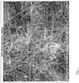
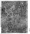
- a SEM/EDX study has revealed that copper oxide nanowires created with the process of this invention have an average diameter in the range of about 20 to about 80 nm.
- An SPC study on conventional weight gain versus nano-oxide specific gravity has demonstrated that nano-oxide coatings in accordance with the present invention have an average thickness in the range of about 50 nm to about 100 nm.
- the enhanced passivate nano-oxide coatings described herein are useful in any application directed to copper/copper alloy bonding to a dielectric material, especially in printed circuit board fabrication and packaging and in applications dedicated to the high speed/low loss electronics market.
- An oxide bath (without organics) not in accordance with the claimed invention was prepared comprising: 225 g/l sodium chlorite 8.4 g/l sodium hydroxide 6.5 g/l potassium phosphate
- a nano-oxide bath comprising: 225 g/l sodium chlorite 8.4 g/l sodium hydroxide 6.5 g/l potassium phosphate 115 ppm 3,5-dinitrosalicylic acid 400 ppm sodium thiosulfate
- This bath was used to evaluate the effect of temperature of the nano-wire diameter on the copper surface.
- This bath was applied to copper surfaces at temperatures of 35°C, 45°C, 50°C°, 56°C, 60°C and 70°C.
- the application of the composition at higher temperatures produced nano-wires having significantly smaller diameters than at lower temperatures.
- a peel strength test coupon set by a 7.62cm by 11.43cm (3 inch by 4.5 inch) size of double sided copper clad and the same size of copper foil were immersion processed through the following cycle:
- the coupon and foil were de-moisturized at 110°C for 20 minutes prior to layering up with ISOLA 406 Prepreg: 1 of the same size of 7628 Prepreg (both available from Isola Group, Inc., Chandler, AZ) was sandwiched between 2 of the same size of 1080 no-flow prepreg or halogen-free HITACHI HF prepreg in the same construction. The materials were then laminated under designed program per each material.
- test coupons were then worked up through routing, scribing, tapping, selective stripping, detapping, post baking for 2 hours at 110°C and then solder shocked at 288°C for 3 x 10 seconds and 6 x 10 seconds. 2.54cm (one inch) wide copper foil per each test coupon was measured for peel strength in a Peel strength tester.
- Example 4 The same process and bath parameters were used as in Example 3, except the nano-oxide bath in this example 4 also included the following additive system: 3,5-dintro salicylic acid 0.130 g/l Poly(ethylene glycol) 0.5 g/l Sodium thiosulfate 0.2 g/l
- the pre-dip bath comprised the following: Sodium hydroxide 28.0 g/l Potassium phosphate 18.0 g/l
- the oxide bath comprised the following: Sodium chlorite 210 g/l Sodium hydroxide 5.6 g/l Potassium phosphate 16.5 g/l
- the Post-dip bath comprised the following: Phosphoric acid (85%) 20 ml/L Potassium hydroxide (45%) 45+ ml/L to pH at room temperature of 10.50 Sodium molybdate 30 g/l 2-aminothiazole 20 g/l
- test vehicle was processed as in Example 3 and the following peel strengths were observed: TABLE III Prepreg ISOLA 408 Solder shock at 288 °C Peel strength 0 seconds 0.89kg/cm (5.0 lb/in) 3 x 10 seconds 0.79kg/cm (4.4 lb/in) 6 x 10 seconds 0.68kg/cm (3.8 lb/in)
- Example 5 The same process and test parameter as in Example 5 were used except that a reverse treated foil (RTF) foil was tested and replaced the above standard uncoated copper foils.
- RTF reverse treated foil
- the present invention provides excellent peel strength under various conditions and using various materials.
- Table V provides a comparison of the enhanced nano-oxide process described herein with the conventional black oxide and alternative oxide processes of the prior art. Table V. Comparison of Nano-Oxide Process to the Prior Art Oxide Processes Perspective Conventional Black Oxide Alternative Oxide Enhanced Nano Oxide Microetch Yes Yes No Number of Processing steps 6 5 (6 with enhance) 5 Application Vertical Horizontal & Vertical Horizontal & Vertical Total Cycle Time 50 ⁇ 5 minutes 8 ⁇ 1 minute (Optional step may require additional 2-3 minutes) 9 ⁇ 1 minute Total cost High Cost effective Cost saving Waste treatment cost High High Low
- the application can be either horizontal or vertical, which provides a real customized application, including the use of high performance materials.
- the enhanced nano-oxide process described herein also exhibits significant cost savings, especially as compared to both the conventional black oxide and the alternative oxide processes.
- the enhanced nano-oxide process uses only about 1/10 of the chemical consumption of the conventional black oxide process and has very low additive consumption, due to self-determined passivating coating.
- the waste treatment cost of the enhanced nano oxide process of the invention is also low as compared to both the conventional black oxide and the alternative oxide processes because there is no etched copper and much less oxide precipitates and organic waste due to the passivate mechanism.
Landscapes
- Chemical & Material Sciences (AREA)
- Engineering & Computer Science (AREA)
- Metallurgy (AREA)
- Chemical Kinetics & Catalysis (AREA)
- Materials Engineering (AREA)
- Mechanical Engineering (AREA)
- General Chemical & Material Sciences (AREA)
- Organic Chemistry (AREA)
- Inorganic Chemistry (AREA)
- Manufacturing & Machinery (AREA)
- Microelectronics & Electronic Packaging (AREA)
- Chemical Treatment Of Metals (AREA)
- Laminated Bodies (AREA)
Claims (15)
- Nanooxidzusammensetzung zur Verbesserung der Adhäsion zwischen Kupfer oder Kupferlegierung und einem Kunststoff, wobei die Zusammensetzung Folgendes umfasst:(a) ein Chloritsalz;(b) eine Alkalinitätsquelle;(c) ein Phosphatsalz;(d) eine organische Nitroverbindung, die aus aromatischen Nitroverbindungen ausgewählt ist; und(e) eine Thioverbindung, die aus Thioschwefelsäure und Thiosulfatsalzen ausgewählt ist.
- Zusammensetzung nach Anspruch 1, wobei die Konzentration des Chloritsalzes zwischen 150 und 250 g/l liegt.
- Zusammensetzung nach Anspruch 1, wobei die Alkalinitätsquelle aus der Gruppe bestehend aus Kaliumhydroxid und Natriumhydroxid ausgewählt ist,
optional wobei die Alkalinitätsquelle Natriumhydroxid ist oder wobei die Konzentration der Alkalinitätsquelle zwischen 5 und 30 g/l liegt. - Zusammensetzung nach Anspruch 1, wobei das Phosphatsalz aus der Gruppe bestehend aus Lithiumphosphat, Natriumphosphat und Kaliumphosphat ausgewählt ist,
optional wobei das Phosphatsalz Kaliumphosphat ist oder wobei die Konzentration des Phosphatsalzes zwischen 5 und 25 g/l liegt. - Zusammensetzung nach Anspruch 1, wobei die organische Nitroverbindung aus der Gruppe bestehend aus Natrium-meta-nitrobenzolsulfonat, para-Nitrophenol, 3,5-Dinitrosalicylsäure und 3,5-Dinitrobenzoesäure ausgewählt ist,
optional wobei die organische Nitroverbindung 3,5-Dinitrosalicylsäure ist oder wobei die Konzentration der organischen Nitroverbindung zwischen 0,1 und 0,2 g/l liegt. - Zusammensetzung nach Anspruch 1, wobei die Thioverbindung ein Thiosulfatsalz ist, das aus der Gruppe bestehend aus Natriumthiosulfat, Kaliumthiosulfat, Ammoniumthiosulfat und Kombinationen von einem oder mehreren der vorstehenden ausgewählt ist,
optional wobei die Thioverbindung Natriumthiosulfat ist oder wobei die Konzentration der Thioverbindung zwischen 0,2 und 0,8 g/l liegt. - Zusammensetzung nach Anspruch 1, die weiterhin ein Tensid oder wasserlösliches Polymer umfasst,
optional wobei die Konzentration des Tensids oder wasserlöslichen Polymers zwischen 0,25 und 1,5 g/l liegt. - Nachtauchzusammensetzung zur Verbesserung des Bondens einer behandelten Kupferoberfläche an einem Kunststoff, wobei die Zusammensetzung Folgendes umfasst:a) ein Phosphatsalz;b) eine Quelle von Molybdän-Ionen undc) ein Thiazol.
- Nachtauchzusammensetzung nach Anspruch 8, wobei das Phosphatsalz aus der Gruppe bestehend aus Lithiumphosphat, Natriumphosphat und Kaliumphosphat ausgewählt ist,
optional wobei das Phosphatsalz Kaliumphosphat umfasst,
weiterhin optional wobei die Konzentration des Phosphatsalzes zwischen 5 g/l und 25 g/l liegt. - Nachtauchzusammensetzung nach Anspruch 8, wobei die Quelle von Molybdän-Ionen aus der Gruppe bestehend aus Natriummolybdat, Phosphomolybdänsäure, Molybdänsäure, Molybdänsäureanhydrid und Salzen von Phosphomolybdänsäure ausgewählt ist,
optional wobei die Quelle von Molybdän-Ionen Natriummolybdat ist oder wobei die Konzentration der Quelle von Molybdän-Ionen zwischen 20 und 40 g/l liegt. - Nachtauchzusammensetzung nach Anspruch 8, wobei das Thiazol aus der Gruppe bestehend aus Aminothiazolen und substituierten Aminothiazolen ausgewählt ist,
optional wobei das Thiazol 2-Aminothiazol ist oder wobei die Konzentration des Thiazols zwischen 5 und 30 g/l liegt. - Nachtauchzusammensetzung nach Anspruch 8, wobei die Zusammensetzung einen pH-Wert zwischen 9 und 11 aufweist.
- Verfahren zur Erhöhung der Adhäsion zwischen einer Kupfer- oder Kupferlegierungsschicht und einem polymeren Kunststoff, wobei das Verfahren die folgenden Schritte umfasst:a) Aufbringen einer Vortauchzusammensetzung auf die Kupferschicht;b) Aufbringen einer Nanooxidzusammensetzung nach einem der Ansprüche 1 bis 7 auf die behandelte Kupferschicht;c) Aufbringen einer Nachtauchzusammensetzung auf die mit Nanooxid behandelte Oberfläche undd) danach Bonden eines Kunststoffs an die behandelte Kupferoberfläche.
- Verfahren nach Anspruch 13, wobei ein Mikroätzschritt nicht durchgeführt wird,
oder wobei die Nachtauchzusammensetzung eine Zusammensetzung nach Anspruch 8 oder nach einem der Ansprüche 10 bis 12 ist, optional wobei die Nachtauchzusammensetzung bei einer Temperatur zwischen 45 und 55 °C aufgebracht wird. - Verfahren nach Anspruch 13, wobei die Nachtauchzusammensetzung ein Phosphatsalz und eine Alkalinitätsquelle umfasst,
oder wobei die Nanooxidbeschichtung bei einer Temperatur zwischen 65 und 75 °C aufgebracht wird.
Applications Claiming Priority (2)
| Application Number | Priority Date | Filing Date | Title |
|---|---|---|---|
| US12/697,425 US8308893B2 (en) | 2010-02-01 | 2010-02-01 | Nano-oxide process for bonding copper/copper alloy and resin |
| PCT/US2010/058312 WO2011093943A2 (en) | 2010-02-01 | 2010-11-30 | Nano-oxide process for bonding copper/copper alloy and resin |
Publications (3)
| Publication Number | Publication Date |
|---|---|
| EP2531350A2 EP2531350A2 (de) | 2012-12-12 |
| EP2531350A4 EP2531350A4 (de) | 2018-01-10 |
| EP2531350B1 true EP2531350B1 (de) | 2019-02-27 |
Family
ID=44320032
Family Applications (1)
| Application Number | Title | Priority Date | Filing Date |
|---|---|---|---|
| EP10844927.3A Active EP2531350B1 (de) | 2010-02-01 | 2010-11-30 | Nano-oxid-verfahren zum bonden einer kupfer-/kupferlegierung und harz |
Country Status (6)
| Country | Link |
|---|---|
| US (1) | US8308893B2 (de) |
| EP (1) | EP2531350B1 (de) |
| CN (1) | CN103167953B (de) |
| ES (1) | ES2718841T3 (de) |
| TW (1) | TWI414629B (de) |
| WO (1) | WO2011093943A2 (de) |
Families Citing this family (7)
| Publication number | Priority date | Publication date | Assignee | Title |
|---|---|---|---|---|
| CN104694909B (zh) * | 2014-07-03 | 2017-01-25 | 广东丹邦科技有限公司 | 一种铜表面粗化剂 |
| JP6832581B2 (ja) * | 2016-07-15 | 2021-02-24 | ナミックス株式会社 | プリント配線板に用いる銅箔の製造方法 |
| EP3911781A1 (de) * | 2019-01-15 | 2021-11-24 | ATOTECH Deutschland GmbH | Verfahren zur herstellung von kupferoxid auf einer kupferoberfläche |
| CN110029336B (zh) * | 2019-05-24 | 2021-05-14 | 电子科技大学 | 一种多层印制电路板制造用铜表面处理液及处理方法 |
| CN110125386B (zh) * | 2019-05-29 | 2022-01-11 | 深圳第三代半导体研究院 | 一种表面进行抗氧化保护的铜颗粒的形成方法、低温烧结铜膏及使用其的烧结工艺 |
| JP2022099497A (ja) * | 2020-12-23 | 2022-07-05 | セイコーエプソン株式会社 | 電気光学装置及び電子機器 |
| KR20240018632A (ko) | 2021-06-09 | 2024-02-13 | 아토테크 도이칠란트 게엠베하 운트 콤파니 카게 | 구리층과 유기층의 복합재 및 그 복합재의 제조방법 |
Family Cites Families (32)
| Publication number | Priority date | Publication date | Assignee | Title |
|---|---|---|---|---|
| US2364993A (en) | 1942-12-29 | 1944-12-12 | Walter R Meyer | Process for blackening copper or copper alloy surfaces |
| US3816186A (en) * | 1972-11-09 | 1974-06-11 | Conversion Chem Corp | Composition and method for producing brown coating on brass |
| US4130455A (en) * | 1977-11-08 | 1978-12-19 | Dart Industries Inc. | Dissolution of metals-utilizing H2 O2 -H2 SO4 -thiosulfate etchant |
| US4409037A (en) | 1982-04-05 | 1983-10-11 | Macdermid Incorporated | Adhesion promoter for printed circuits |
| US4844981A (en) | 1982-04-05 | 1989-07-04 | Macdermid, Incorporated | Adhesion promoter for printed circuits |
| US4643161A (en) | 1984-07-05 | 1987-02-17 | Kim George A | Method of machining hard and brittle material |
| JPS61176192A (ja) | 1985-01-31 | 1986-08-07 | 株式会社日立製作所 | 銅と樹脂との接着方法 |
| US4775444A (en) * | 1987-08-26 | 1988-10-04 | Macdermid, Incorporated | Process for fabricating multilayer circuit boards |
| JPH0713304B2 (ja) | 1987-12-14 | 1995-02-15 | 日立化成工業株式会社 | 銅の表面処理法 |
| JPH01246393A (ja) | 1988-03-25 | 1989-10-02 | Fukuda Metal Foil & Powder Co Ltd | 内層用銅箔または銅張積層板の表面処理方法 |
| US4969958A (en) | 1989-03-30 | 1990-11-13 | Rd Chemical Company | Process and composition for forming black oxide layers |
| US4997722A (en) | 1989-07-10 | 1991-03-05 | Edward Adler | Composition and method for improving adherence of copper foil to resinous substrates |
| US4997516A (en) | 1989-07-10 | 1991-03-05 | Edward Adler | Method for improving adherence of copper foil to resinous substrates |
| US5289630A (en) | 1991-07-22 | 1994-03-01 | Macdermid, Incorporated | Process for fabricating multilayer printed circuits |
| WO1993010277A1 (en) * | 1991-11-20 | 1993-05-27 | Electrochemicals, Inc. | Improved method for bonding copper to a polymeric material |
| ATE239799T1 (de) | 1995-09-07 | 2003-05-15 | Novozymes As | Nachweis der aktivität von enzymen für detergenzien durch phagen. |
| US6162503A (en) | 1997-06-12 | 2000-12-19 | Macdermid, Incorporated | Process for improving the adhesion of polymeric materials to metal surfaces |
| US6020029A (en) | 1997-06-12 | 2000-02-01 | Macdermid, Incorporated | Process for treating metal surfaces |
| US5869130A (en) | 1997-06-12 | 1999-02-09 | Mac Dermid, Incorporated | Process for improving the adhesion of polymeric materials to metal surfaces |
| US6146701A (en) | 1997-06-12 | 2000-11-14 | Macdermid, Incorporated | Process for improving the adhension of polymeric materials to metal surfaces |
| US6054061A (en) | 1997-12-11 | 2000-04-25 | Shipley Company, L.L.C. | Composition for circuit board manufacture |
| US6444140B2 (en) | 1999-03-17 | 2002-09-03 | Morton International Inc. | Micro-etch solution for producing metal surface topography |
| US6830627B1 (en) | 1999-03-23 | 2004-12-14 | International Business Machines Corporation | Copper cleaning compositions, processes and products derived therefrom |
| US6383272B1 (en) * | 2000-06-08 | 2002-05-07 | Donald Ferrier | Process for improving the adhesion of polymeric materials to metal surfaces |
| US6419784B1 (en) | 2000-06-21 | 2002-07-16 | Donald Ferrier | Process for improving the adhesion of polymeric materials to metal surfaces |
| US6554948B1 (en) | 2000-08-22 | 2003-04-29 | Donald Ferrier | Process for improving the adhesion of polymeric materials to metal surfaces |
| EP1209253A3 (de) | 2000-11-28 | 2004-02-25 | Shipley Co. L.L.C. | Verfahren zur Behandlung von gut haftenden Metalloberflächen mit Epoxidharzen |
| US20060065365A1 (en) * | 2004-09-30 | 2006-03-30 | Ferrier Donald R | Melamine-formaldehyde post-dip composition for improving adhesion of metal to polymer |
| JP2006213958A (ja) * | 2005-02-02 | 2006-08-17 | Nippon Parkerizing Co Ltd | 金属材料表面処理用組成物及び処理方法 |
| JP2006249519A (ja) * | 2005-03-11 | 2006-09-21 | Hitachi Chem Co Ltd | 銅の表面処理方法及び銅 |
| US7588835B2 (en) | 2005-03-11 | 2009-09-15 | Hitachi Chemical Company, Ltd. | Method of treating the surface of copper and copper |
| US8518281B2 (en) | 2008-06-03 | 2013-08-27 | Kesheng Feng | Acid-resistance promoting composition |
-
2010
- 2010-02-01 US US12/697,425 patent/US8308893B2/en active Active
- 2010-11-30 CN CN201080062853.8A patent/CN103167953B/zh active Active
- 2010-11-30 ES ES10844927T patent/ES2718841T3/es active Active
- 2010-11-30 EP EP10844927.3A patent/EP2531350B1/de active Active
- 2010-11-30 WO PCT/US2010/058312 patent/WO2011093943A2/en not_active Ceased
- 2010-12-17 TW TW099144447A patent/TWI414629B/zh active
Non-Patent Citations (1)
| Title |
|---|
| None * |
Also Published As
| Publication number | Publication date |
|---|---|
| US8308893B2 (en) | 2012-11-13 |
| CN103167953B (zh) | 2015-08-26 |
| ES2718841T3 (es) | 2019-07-04 |
| WO2011093943A3 (en) | 2014-03-27 |
| CN103167953A (zh) | 2013-06-19 |
| US20110186221A1 (en) | 2011-08-04 |
| EP2531350A4 (de) | 2018-01-10 |
| WO2011093943A2 (en) | 2011-08-04 |
| EP2531350A2 (de) | 2012-12-12 |
| TW201131013A (en) | 2011-09-16 |
| TWI414629B (zh) | 2013-11-11 |
Similar Documents
| Publication | Publication Date | Title |
|---|---|---|
| US5869130A (en) | Process for improving the adhesion of polymeric materials to metal surfaces | |
| EP2531350B1 (de) | Nano-oxid-verfahren zum bonden einer kupfer-/kupferlegierung und harz | |
| EP1681373B1 (de) | Zusammensetzung zur Verbesserung der Haftfähigkeit von Polymeren an der Metalloberflächen | |
| EP2051820A2 (de) | Verfahren zur verbesserung der haftung von polymermaterialien auf metalloberflächen | |
| EP1311644B1 (de) | Verfahren zur steigerung der adhäsion von polymeren an metallen | |
| EP0984672B1 (de) | Verfahren zur Behandlung von Metalloberflächen | |
| US7186305B2 (en) | Process for improving the adhesion of polymeric materials to metal surfaces | |
| EP1020503B1 (de) | Verfahren zur Verbesserung der Adhäsion von Polymeren an Metalloberflächen | |
| US6162503A (en) | Process for improving the adhesion of polymeric materials to metal surfaces | |
| US8512504B2 (en) | Process for improving adhesion of polymeric materials to metal surfaces | |
| EP1158843B1 (de) | Verfahren zur Verbesserung der Adhäsion von Polymermaterialien an Metalloberflächen | |
| EP1794351B1 (de) | Melamin-formaldeyhd-post-dip-zusammensetzung zur verbesserung der haftung von metall auf polymer |
Legal Events
| Date | Code | Title | Description |
|---|---|---|---|
| PUAI | Public reference made under article 153(3) epc to a published international application that has entered the european phase |
Free format text: ORIGINAL CODE: 0009012 |
|
| 17P | Request for examination filed |
Effective date: 20120831 |
|
| AK | Designated contracting states |
Kind code of ref document: A2 Designated state(s): AL AT BE BG CH CY CZ DE DK EE ES FI FR GB GR HR HU IE IS IT LI LT LU LV MC MK MT NL NO PL PT RO RS SE SI SK SM TR |
|
| DAX | Request for extension of the european patent (deleted) | ||
| R17D | Deferred search report published (corrected) |
Effective date: 20140327 |
|
| A4 | Supplementary search report drawn up and despatched |
Effective date: 20171211 |
|
| RIC1 | Information provided on ipc code assigned before grant |
Ipc: B32B 7/12 20060101AFI20171205BHEP Ipc: C09D 5/00 20060101ALI20171205BHEP Ipc: C08K 5/32 20060101ALI20171205BHEP Ipc: C23C 22/63 20060101ALI20171205BHEP Ipc: H05K 3/38 20060101ALI20171205BHEP Ipc: C23C 22/78 20060101ALI20171205BHEP Ipc: C23C 22/83 20060101ALI20171205BHEP |
|
| GRAP | Despatch of communication of intention to grant a patent |
Free format text: ORIGINAL CODE: EPIDOSNIGR1 |
|
| STAA | Information on the status of an ep patent application or granted ep patent |
Free format text: STATUS: GRANT OF PATENT IS INTENDED |
|
| RIC1 | Information provided on ipc code assigned before grant |
Ipc: H05K 3/38 20060101ALI20180731BHEP Ipc: C23C 22/83 20060101ALI20180731BHEP Ipc: B32B 7/12 20060101AFI20180731BHEP Ipc: C08K 5/32 20060101ALI20180731BHEP Ipc: C23C 22/78 20060101ALI20180731BHEP Ipc: C23C 22/63 20060101ALI20180731BHEP Ipc: C09D 5/00 20060101ALI20180731BHEP |
|
| INTG | Intention to grant announced |
Effective date: 20180820 |
|
| GRAS | Grant fee paid |
Free format text: ORIGINAL CODE: EPIDOSNIGR3 |
|
| GRAJ | Information related to disapproval of communication of intention to grant by the applicant or resumption of examination proceedings by the epo deleted |
Free format text: ORIGINAL CODE: EPIDOSDIGR1 |
|
| GRAL | Information related to payment of fee for publishing/printing deleted |
Free format text: ORIGINAL CODE: EPIDOSDIGR3 |
|
| STAA | Information on the status of an ep patent application or granted ep patent |
Free format text: STATUS: REQUEST FOR EXAMINATION WAS MADE |
|
| GRAR | Information related to intention to grant a patent recorded |
Free format text: ORIGINAL CODE: EPIDOSNIGR71 |
|
| STAA | Information on the status of an ep patent application or granted ep patent |
Free format text: STATUS: GRANT OF PATENT IS INTENDED |
|
| GRAA | (expected) grant |
Free format text: ORIGINAL CODE: 0009210 |
|
| STAA | Information on the status of an ep patent application or granted ep patent |
Free format text: STATUS: THE PATENT HAS BEEN GRANTED |
|
| INTC | Intention to grant announced (deleted) | ||
| AK | Designated contracting states |
Kind code of ref document: B1 Designated state(s): AL AT BE BG CH CY CZ DE DK EE ES FI FR GB GR HR HU IE IS IT LI LT LU LV MC MK MT NL NO PL PT RO RS SE SI SK SM TR |
|
| INTG | Intention to grant announced |
Effective date: 20190122 |
|
| REG | Reference to a national code |
Ref country code: GB Ref legal event code: FG4D |
|
| REG | Reference to a national code |
Ref country code: CH Ref legal event code: EP |
|
| REG | Reference to a national code |
Ref country code: AT Ref legal event code: REF Ref document number: 1100738 Country of ref document: AT Kind code of ref document: T Effective date: 20190315 |
|
| REG | Reference to a national code |
Ref country code: IE Ref legal event code: FG4D |
|
| REG | Reference to a national code |
Ref country code: DE Ref legal event code: R096 Ref document number: 602010057310 Country of ref document: DE |
|
| REG | Reference to a national code |
Ref country code: DE Ref legal event code: R082 Ref document number: 602010057310 Country of ref document: DE Representative=s name: PAGE, WHITE & FARRER GERMANY LLP, DE |
|
| REG | Reference to a national code |
Ref country code: NL Ref legal event code: MP Effective date: 20190227 |
|
| REG | Reference to a national code |
Ref country code: ES Ref legal event code: FG2A Ref document number: 2718841 Country of ref document: ES Kind code of ref document: T3 Effective date: 20190704 |
|
| REG | Reference to a national code |
Ref country code: LT Ref legal event code: MG4D |
|
| PG25 | Lapsed in a contracting state [announced via postgrant information from national office to epo] |
Ref country code: FI Free format text: LAPSE BECAUSE OF FAILURE TO SUBMIT A TRANSLATION OF THE DESCRIPTION OR TO PAY THE FEE WITHIN THE PRESCRIBED TIME-LIMIT Effective date: 20190227 Ref country code: NO Free format text: LAPSE BECAUSE OF FAILURE TO SUBMIT A TRANSLATION OF THE DESCRIPTION OR TO PAY THE FEE WITHIN THE PRESCRIBED TIME-LIMIT Effective date: 20190527 Ref country code: LT Free format text: LAPSE BECAUSE OF FAILURE TO SUBMIT A TRANSLATION OF THE DESCRIPTION OR TO PAY THE FEE WITHIN THE PRESCRIBED TIME-LIMIT Effective date: 20190227 Ref country code: NL Free format text: LAPSE BECAUSE OF FAILURE TO SUBMIT A TRANSLATION OF THE DESCRIPTION OR TO PAY THE FEE WITHIN THE PRESCRIBED TIME-LIMIT Effective date: 20190227 Ref country code: SE Free format text: LAPSE BECAUSE OF FAILURE TO SUBMIT A TRANSLATION OF THE DESCRIPTION OR TO PAY THE FEE WITHIN THE PRESCRIBED TIME-LIMIT Effective date: 20190227 Ref country code: PT Free format text: LAPSE BECAUSE OF FAILURE TO SUBMIT A TRANSLATION OF THE DESCRIPTION OR TO PAY THE FEE WITHIN THE PRESCRIBED TIME-LIMIT Effective date: 20190627 |
|
| PG25 | Lapsed in a contracting state [announced via postgrant information from national office to epo] |
Ref country code: LV Free format text: LAPSE BECAUSE OF FAILURE TO SUBMIT A TRANSLATION OF THE DESCRIPTION OR TO PAY THE FEE WITHIN THE PRESCRIBED TIME-LIMIT Effective date: 20190227 Ref country code: RS Free format text: LAPSE BECAUSE OF FAILURE TO SUBMIT A TRANSLATION OF THE DESCRIPTION OR TO PAY THE FEE WITHIN THE PRESCRIBED TIME-LIMIT Effective date: 20190227 Ref country code: IS Free format text: LAPSE BECAUSE OF FAILURE TO SUBMIT A TRANSLATION OF THE DESCRIPTION OR TO PAY THE FEE WITHIN THE PRESCRIBED TIME-LIMIT Effective date: 20190627 Ref country code: BG Free format text: LAPSE BECAUSE OF FAILURE TO SUBMIT A TRANSLATION OF THE DESCRIPTION OR TO PAY THE FEE WITHIN THE PRESCRIBED TIME-LIMIT Effective date: 20190527 Ref country code: GR Free format text: LAPSE BECAUSE OF FAILURE TO SUBMIT A TRANSLATION OF THE DESCRIPTION OR TO PAY THE FEE WITHIN THE PRESCRIBED TIME-LIMIT Effective date: 20190528 Ref country code: HR Free format text: LAPSE BECAUSE OF FAILURE TO SUBMIT A TRANSLATION OF THE DESCRIPTION OR TO PAY THE FEE WITHIN THE PRESCRIBED TIME-LIMIT Effective date: 20190227 |
|
| REG | Reference to a national code |
Ref country code: AT Ref legal event code: MK05 Ref document number: 1100738 Country of ref document: AT Kind code of ref document: T Effective date: 20190227 |
|
| PG25 | Lapsed in a contracting state [announced via postgrant information from national office to epo] |
Ref country code: DK Free format text: LAPSE BECAUSE OF FAILURE TO SUBMIT A TRANSLATION OF THE DESCRIPTION OR TO PAY THE FEE WITHIN THE PRESCRIBED TIME-LIMIT Effective date: 20190227 Ref country code: EE Free format text: LAPSE BECAUSE OF FAILURE TO SUBMIT A TRANSLATION OF THE DESCRIPTION OR TO PAY THE FEE WITHIN THE PRESCRIBED TIME-LIMIT Effective date: 20190227 Ref country code: SK Free format text: LAPSE BECAUSE OF FAILURE TO SUBMIT A TRANSLATION OF THE DESCRIPTION OR TO PAY THE FEE WITHIN THE PRESCRIBED TIME-LIMIT Effective date: 20190227 Ref country code: AL Free format text: LAPSE BECAUSE OF FAILURE TO SUBMIT A TRANSLATION OF THE DESCRIPTION OR TO PAY THE FEE WITHIN THE PRESCRIBED TIME-LIMIT Effective date: 20190227 Ref country code: RO Free format text: LAPSE BECAUSE OF FAILURE TO SUBMIT A TRANSLATION OF THE DESCRIPTION OR TO PAY THE FEE WITHIN THE PRESCRIBED TIME-LIMIT Effective date: 20190227 Ref country code: CZ Free format text: LAPSE BECAUSE OF FAILURE TO SUBMIT A TRANSLATION OF THE DESCRIPTION OR TO PAY THE FEE WITHIN THE PRESCRIBED TIME-LIMIT Effective date: 20190227 |
|
| REG | Reference to a national code |
Ref country code: DE Ref legal event code: R097 Ref document number: 602010057310 Country of ref document: DE |
|
| PG25 | Lapsed in a contracting state [announced via postgrant information from national office to epo] |
Ref country code: SM Free format text: LAPSE BECAUSE OF FAILURE TO SUBMIT A TRANSLATION OF THE DESCRIPTION OR TO PAY THE FEE WITHIN THE PRESCRIBED TIME-LIMIT Effective date: 20190227 Ref country code: PL Free format text: LAPSE BECAUSE OF FAILURE TO SUBMIT A TRANSLATION OF THE DESCRIPTION OR TO PAY THE FEE WITHIN THE PRESCRIBED TIME-LIMIT Effective date: 20190227 |
|
| PG25 | Lapsed in a contracting state [announced via postgrant information from national office to epo] |
Ref country code: AT Free format text: LAPSE BECAUSE OF FAILURE TO SUBMIT A TRANSLATION OF THE DESCRIPTION OR TO PAY THE FEE WITHIN THE PRESCRIBED TIME-LIMIT Effective date: 20190227 |
|
| PLBE | No opposition filed within time limit |
Free format text: ORIGINAL CODE: 0009261 |
|
| STAA | Information on the status of an ep patent application or granted ep patent |
Free format text: STATUS: NO OPPOSITION FILED WITHIN TIME LIMIT |
|
| 26N | No opposition filed |
Effective date: 20191128 |
|
| PG25 | Lapsed in a contracting state [announced via postgrant information from national office to epo] |
Ref country code: SI Free format text: LAPSE BECAUSE OF FAILURE TO SUBMIT A TRANSLATION OF THE DESCRIPTION OR TO PAY THE FEE WITHIN THE PRESCRIBED TIME-LIMIT Effective date: 20190227 |
|
| PG25 | Lapsed in a contracting state [announced via postgrant information from national office to epo] |
Ref country code: TR Free format text: LAPSE BECAUSE OF FAILURE TO SUBMIT A TRANSLATION OF THE DESCRIPTION OR TO PAY THE FEE WITHIN THE PRESCRIBED TIME-LIMIT Effective date: 20190227 |
|
| REG | Reference to a national code |
Ref country code: CH Ref legal event code: PL |
|
| PG25 | Lapsed in a contracting state [announced via postgrant information from national office to epo] |
Ref country code: CH Free format text: LAPSE BECAUSE OF NON-PAYMENT OF DUE FEES Effective date: 20191130 Ref country code: LU Free format text: LAPSE BECAUSE OF NON-PAYMENT OF DUE FEES Effective date: 20191130 Ref country code: LI Free format text: LAPSE BECAUSE OF NON-PAYMENT OF DUE FEES Effective date: 20191130 Ref country code: MC Free format text: LAPSE BECAUSE OF FAILURE TO SUBMIT A TRANSLATION OF THE DESCRIPTION OR TO PAY THE FEE WITHIN THE PRESCRIBED TIME-LIMIT Effective date: 20190227 |
|
| REG | Reference to a national code |
Ref country code: BE Ref legal event code: MM Effective date: 20191130 |
|
| PG25 | Lapsed in a contracting state [announced via postgrant information from national office to epo] |
Ref country code: IE Free format text: LAPSE BECAUSE OF NON-PAYMENT OF DUE FEES Effective date: 20191130 |
|
| PG25 | Lapsed in a contracting state [announced via postgrant information from national office to epo] |
Ref country code: BE Free format text: LAPSE BECAUSE OF NON-PAYMENT OF DUE FEES Effective date: 20191130 |
|
| PG25 | Lapsed in a contracting state [announced via postgrant information from national office to epo] |
Ref country code: CY Free format text: LAPSE BECAUSE OF FAILURE TO SUBMIT A TRANSLATION OF THE DESCRIPTION OR TO PAY THE FEE WITHIN THE PRESCRIBED TIME-LIMIT Effective date: 20190227 |
|
| PG25 | Lapsed in a contracting state [announced via postgrant information from national office to epo] |
Ref country code: MT Free format text: LAPSE BECAUSE OF FAILURE TO SUBMIT A TRANSLATION OF THE DESCRIPTION OR TO PAY THE FEE WITHIN THE PRESCRIBED TIME-LIMIT Effective date: 20190227 Ref country code: HU Free format text: LAPSE BECAUSE OF FAILURE TO SUBMIT A TRANSLATION OF THE DESCRIPTION OR TO PAY THE FEE WITHIN THE PRESCRIBED TIME-LIMIT; INVALID AB INITIO Effective date: 20101130 |
|
| PG25 | Lapsed in a contracting state [announced via postgrant information from national office to epo] |
Ref country code: MK Free format text: LAPSE BECAUSE OF FAILURE TO SUBMIT A TRANSLATION OF THE DESCRIPTION OR TO PAY THE FEE WITHIN THE PRESCRIBED TIME-LIMIT Effective date: 20190227 |
|
| P01 | Opt-out of the competence of the unified patent court (upc) registered |
Effective date: 20230524 |
|
| REG | Reference to a national code |
Ref country code: DE Ref legal event code: R082 Ref document number: 602010057310 Country of ref document: DE Representative=s name: WESTPHAL, MUSSGNUG & PARTNER PATENTANWAELTE MI, DE |
|
| PGFP | Annual fee paid to national office [announced via postgrant information from national office to epo] |
Ref country code: DE Payment date: 20251022 Year of fee payment: 16 |
|
| PGFP | Annual fee paid to national office [announced via postgrant information from national office to epo] |
Ref country code: GB Payment date: 20251023 Year of fee payment: 16 |
|
| PGFP | Annual fee paid to national office [announced via postgrant information from national office to epo] |
Ref country code: IT Payment date: 20251022 Year of fee payment: 16 |
|
| PGFP | Annual fee paid to national office [announced via postgrant information from national office to epo] |
Ref country code: FR Payment date: 20251023 Year of fee payment: 16 |
|
| PGFP | Annual fee paid to national office [announced via postgrant information from national office to epo] |
Ref country code: ES Payment date: 20251201 Year of fee payment: 16 |