EP2530833A2 - HF-Verstärker mit offenem Schaltungsausgang im Aus-Zustand - Google Patents
HF-Verstärker mit offenem Schaltungsausgang im Aus-Zustand Download PDFInfo
- Publication number
- EP2530833A2 EP2530833A2 EP12163913A EP12163913A EP2530833A2 EP 2530833 A2 EP2530833 A2 EP 2530833A2 EP 12163913 A EP12163913 A EP 12163913A EP 12163913 A EP12163913 A EP 12163913A EP 2530833 A2 EP2530833 A2 EP 2530833A2
- Authority
- EP
- European Patent Office
- Prior art keywords
- amplifier
- receive
- transmit
- coupling
- switch
- Prior art date
- Legal status (The legal status is an assumption and is not a legal conclusion. Google has not performed a legal analysis and makes no representation as to the accuracy of the status listed.)
- Withdrawn
Links
- 230000008878 coupling Effects 0.000 claims abstract description 45
- 238000010168 coupling process Methods 0.000 claims abstract description 45
- 238000005859 coupling reaction Methods 0.000 claims abstract description 45
- 238000000034 method Methods 0.000 claims abstract description 34
- 230000004048 modification Effects 0.000 description 5
- 238000012986 modification Methods 0.000 description 5
- 239000003990 capacitor Substances 0.000 description 4
- 238000010586 diagram Methods 0.000 description 4
- 230000002457 bidirectional effect Effects 0.000 description 2
- 230000005540 biological transmission Effects 0.000 description 2
- 238000004519 manufacturing process Methods 0.000 description 2
- 230000003068 static effect Effects 0.000 description 2
- 230000008901 benefit Effects 0.000 description 1
- 230000015556 catabolic process Effects 0.000 description 1
- 230000008859 change Effects 0.000 description 1
- 238000006731 degradation reaction Methods 0.000 description 1
- 230000000694 effects Effects 0.000 description 1
- 230000005669 field effect Effects 0.000 description 1
- 230000003071 parasitic effect Effects 0.000 description 1
Images


Classifications
-
- H—ELECTRICITY
- H03—ELECTRONIC CIRCUITRY
- H03F—AMPLIFIERS
- H03F3/00—Amplifiers with only discharge tubes or only semiconductor devices as amplifying elements
- H03F3/72—Gated amplifiers, i.e. amplifiers which are rendered operative or inoperative by means of a control signal
-
- H—ELECTRICITY
- H03—ELECTRONIC CIRCUITRY
- H03F—AMPLIFIERS
- H03F1/00—Details of amplifiers with only discharge tubes, only semiconductor devices or only unspecified devices as amplifying elements
- H03F1/56—Modifications of input or output impedances, not otherwise provided for
-
- H—ELECTRICITY
- H03—ELECTRONIC CIRCUITRY
- H03F—AMPLIFIERS
- H03F3/00—Amplifiers with only discharge tubes or only semiconductor devices as amplifying elements
- H03F3/189—High-frequency amplifiers, e.g. radio frequency amplifiers
- H03F3/19—High-frequency amplifiers, e.g. radio frequency amplifiers with semiconductor devices only
- H03F3/193—High-frequency amplifiers, e.g. radio frequency amplifiers with semiconductor devices only with field-effect devices
-
- H—ELECTRICITY
- H03—ELECTRONIC CIRCUITRY
- H03F—AMPLIFIERS
- H03F3/00—Amplifiers with only discharge tubes or only semiconductor devices as amplifying elements
- H03F3/20—Power amplifiers, e.g. Class B amplifiers, Class C amplifiers
- H03F3/24—Power amplifiers, e.g. Class B amplifiers, Class C amplifiers of transmitter output stages
- H03F3/245—Power amplifiers, e.g. Class B amplifiers, Class C amplifiers of transmitter output stages with semiconductor devices only
-
- H—ELECTRICITY
- H03—ELECTRONIC CIRCUITRY
- H03F—AMPLIFIERS
- H03F3/00—Amplifiers with only discharge tubes or only semiconductor devices as amplifying elements
- H03F3/60—Amplifiers in which coupling networks have distributed constants, e.g. with waveguide resonators
- H03F3/601—Amplifiers in which coupling networks have distributed constants, e.g. with waveguide resonators using FET's, e.g. GaAs FET's
-
- H—ELECTRICITY
- H03—ELECTRONIC CIRCUITRY
- H03F—AMPLIFIERS
- H03F2200/00—Indexing scheme relating to amplifiers
- H03F2200/15—Indexing scheme relating to amplifiers the supply or bias voltage or current at the drain side of a FET being continuously controlled by a controlling signal
-
- H—ELECTRICITY
- H03—ELECTRONIC CIRCUITRY
- H03F—AMPLIFIERS
- H03F2200/00—Indexing scheme relating to amplifiers
- H03F2200/18—Indexing scheme relating to amplifiers the bias of the gate of a FET being controlled by a control signal
-
- H—ELECTRICITY
- H03—ELECTRONIC CIRCUITRY
- H03F—AMPLIFIERS
- H03F2200/00—Indexing scheme relating to amplifiers
- H03F2200/27—A biasing circuit node being switched in an amplifier circuit
-
- H—ELECTRICITY
- H03—ELECTRONIC CIRCUITRY
- H03F—AMPLIFIERS
- H03F2200/00—Indexing scheme relating to amplifiers
- H03F2200/294—Indexing scheme relating to amplifiers the amplifier being a low noise amplifier [LNA]
-
- H—ELECTRICITY
- H03—ELECTRONIC CIRCUITRY
- H03F—AMPLIFIERS
- H03F2200/00—Indexing scheme relating to amplifiers
- H03F2200/414—A switch being coupled in the output circuit of an amplifier to switch the output on/off
-
- H—ELECTRICITY
- H03—ELECTRONIC CIRCUITRY
- H03F—AMPLIFIERS
- H03F2200/00—Indexing scheme relating to amplifiers
- H03F2200/417—A switch coupled in the output circuit of an amplifier being controlled by a circuit
-
- H—ELECTRICITY
- H03—ELECTRONIC CIRCUITRY
- H03F—AMPLIFIERS
- H03F2200/00—Indexing scheme relating to amplifiers
- H03F2200/423—Amplifier output adaptation especially for transmission line coupling purposes, e.g. impedance adaptation
-
- H—ELECTRICITY
- H03—ELECTRONIC CIRCUITRY
- H03F—AMPLIFIERS
- H03F2200/00—Indexing scheme relating to amplifiers
- H03F2200/541—Transformer coupled at the output of an amplifier
-
- H—ELECTRICITY
- H03—ELECTRONIC CIRCUITRY
- H03F—AMPLIFIERS
- H03F2203/00—Indexing scheme relating to amplifiers with only discharge tubes or only semiconductor devices as amplifying elements covered by H03F3/00
- H03F2203/72—Indexing scheme relating to gated amplifiers, i.e. amplifiers which are rendered operative or inoperative by means of a control signal
- H03F2203/7215—Indexing scheme relating to gated amplifiers, i.e. amplifiers which are rendered operative or inoperative by means of a control signal the gated amplifier being switched on or off by a switch at the input of the amplifier
-
- H—ELECTRICITY
- H03—ELECTRONIC CIRCUITRY
- H03F—AMPLIFIERS
- H03F2203/00—Indexing scheme relating to amplifiers with only discharge tubes or only semiconductor devices as amplifying elements covered by H03F3/00
- H03F2203/72—Indexing scheme relating to gated amplifiers, i.e. amplifiers which are rendered operative or inoperative by means of a control signal
- H03F2203/7221—Indexing scheme relating to gated amplifiers, i.e. amplifiers which are rendered operative or inoperative by means of a control signal the gated amplifier being switched on or off by a switch at the output of the amplifier
-
- H—ELECTRICITY
- H04—ELECTRIC COMMUNICATION TECHNIQUE
- H04B—TRANSMISSION
- H04B1/00—Details of transmission systems, not covered by a single one of groups H04B3/00 - H04B13/00; Details of transmission systems not characterised by the medium used for transmission
- H04B1/02—Transmitters
- H04B1/04—Circuits
-
- Y—GENERAL TAGGING OF NEW TECHNOLOGICAL DEVELOPMENTS; GENERAL TAGGING OF CROSS-SECTIONAL TECHNOLOGIES SPANNING OVER SEVERAL SECTIONS OF THE IPC; TECHNICAL SUBJECTS COVERED BY FORMER USPC CROSS-REFERENCE ART COLLECTIONS [XRACs] AND DIGESTS
- Y10—TECHNICAL SUBJECTS COVERED BY FORMER USPC
- Y10T—TECHNICAL SUBJECTS COVERED BY FORMER US CLASSIFICATION
- Y10T29/00—Metal working
- Y10T29/49—Method of mechanical manufacture
- Y10T29/49002—Electrical device making
- Y10T29/49117—Conductor or circuit manufacturing
Definitions
- the present invention relates to the field of amplifiers.
- Transmit/receive (TR) chips require a switch network to implement bidirectional operation.
- the loss of this switch network during operation directly effects the noise performance of the amplifier and contributes to the degradation of wireless system range.
- a TR system may include a 3-port "Y-junction" circulator for low-loss/high-power applications that is coupled at a first port to an antenna element/array, at a second port to the input of a receive amplifier, and at a third port to the output of a transmit amplifier.
- the output of the receive amplifier and the input of the transmit amplifier may be coupled to a single pole, double throw static switch, and may be alternately coupled to the antenna and the remainder of the TR system via operation of the switch and the circulator.
- the circulator and the switch when the system is operating in a receive mode, electrically couple the antenna to the remainder of the TR system through the receive amplifier, while also causing the electrical path through the transmit amplifier to be electrically isolated, or decoupled, from the antenna and the remainder of the TR system, thereby enabling a receive signal received by the antenna to be sent to the system processor of the TR system.
- the circulator and switch when the TR system is operating in a transmit mode, electrically decouple the receive amplifier while electrically coupling the antenna to the rest of the TR system via the transmit amplifier, thereby enabling a transmit signal to be sent by the system processor to be radiated by the antenna.
- Embodiments of the present invention operate an amplifier, such as that of a TR system or other electrical system, by enabling the output matching network of the amplifier to operate as half of a single pole, double throw switch when it is in the off state.
- an amplifier such as that of a TR system or other electrical system
- the transistor By employing the transistor from the amplifier, a simple change in the bias voltage of the transistor makes the transistor perform as an RF switch. Accordingly, the need for separate switch circuitry or circulator circuitry coupled to the amplifier is eliminated.
- the number of tuning elements required to operate the TR system may be reduced, while the loss of the TR system may be reduced by nearly the amount of loss that would otherwise be caused by such switch circuitry or circulator circuitry. Furthermore, the amount of space consumed by the TR system and the cost to manufacture the TR system may also be reduced.
- the receive amplifier may act as a low-noise amplifier during a receive mode, while the transmit path through the transmit amplifier effectively acts as an "open" circuit, whereby no signal passes therethrough. While in a transmit mode, however, the transmit amplifier may act as a high-power amplifier, while no signal passes through the receive amplifier or receive path.
- One embodiment of the present invention provides a method of operating an amplifier output of an amplifier as a signal switch, the method including coupling a gate of a switch transistor of the amplifier to a switch signal line, coupling a gate of an amplifier transistor of the amplifier to a gate signal line, and controlling impedance of the amplifier by manipulating gate bias voltages of the transistors via the signal lines.
- Controlling impedance of the amplifier may include enabling an electrical signal to pass through the amplifier in an on mode, and preventing an electrical signal from passing through the amplifier in an off mode.
- the method may further include coupling the signal lines to a system processor and coupling a drain of the amplifier transistor to the system processor, and manipulating gate bias voltages of the transistors may include delivering a control signal to the switch signal line, and manipulating a drain voltage of the drain.
- the method may further include operating tuning elements of the amplifier as one or more quarter-wave shunt switches.
- Controlling impedance of the amplifier may include operating tuning elements of the amplifier.
- the method may further include coupling the gate signal line to an electrode of the switch transistor, and manipulating gate bias voltages of the transistors may include delivering a control signal to the switch signal line and manipulating a drain voltage of the amplifier transistor.
- the method may further include coupling the gate signal line to an electrode of the switch transistor, and delivering a control signal to the switch signal line may couple the gate signal line to a ground.
- the amplifier may be a transmit amplifier
- the switch transistor may be a transmit switch transistor
- the amplifier transistor may be a transmit amplifier transistor
- the switch signal line may be a transmit switch signal line
- the gate signal line may be a transmit gate signal line
- the method may further include coupling a gate of a receive switch transistor of a receive amplifier to a receive switch signal line, coupling a gate of a receive amplifier transistor of the receive amplifier to a receive gate signal line, coupling the output of the receive amplifier to a system processor, coupling an input of the transmit amplifier to the output of the receive amplifier, coupling an input of the receive amplifier to an antenna, coupling the output of the transmit amplifier to the input of the receive amplifier, coupling the switch signal lines to the system processor, and controlling impedances of the amplifiers by manipulating gate bias voltages of the transistors via the signal lines.
- the method may further include designing switch network parasitics of the receive and transmit amplifiers to match the receive and transmit amplifiers.
- Coupling the output of the transmit amplifier to the input of the receive amplifier may include directly coupling the output of the transmit amplifier to the input of the receive amplifier.
- Coupling an input of the transmit amplifier to the output of the receive amplifier may include directly coupling an input of the transmit amplifier to the output of the receive amplifier.
- the method may further include coupling the receive gate signal line to an electrode of the receive switch transistor, and coupling the transmit gate signal line to an electrode of the transmit switch transistor.
- Manipulating gate bias voltages of the transistors may include delivering TR control signals from the system processor to the switch signal lines.
- the method may further include coupling the gate signal lines to the system processor and coupling drains of the amplifier transistors to the system processor, and manipulating gate bias voltages of the transistors may include manipulating drain voltages of the amplifier transistors.
- the method may further include operating tuning elements of the amplifiers to further control impedance of the amplifiers.
- the method may further include operating the receive amplifier with nominal impedance and the transmit amplifier as an open-circuit during a receive mode, detecting a receive signal with the antenna, and delivering the receive signal detected by the antenna to the system processor during the receive mode.
- the method may further include operating the receive amplifier as an open-circuit and the transmit amplifier with nominal impedance during a transmit mode, delivering a transmit signal to the antenna from the system processor during the transmit mode, and radiating the transmit signal delivered to the antenna.
- embodiments of the present invention enable an amplifier to be operated as a switch.
- embodiments of the present invention also enable a TR system to be operated in the absence of switch or circulator circuitry, thereby improving performance of the TR system, while also reducing the size and the cost of manufacture of the TR system.
- Embodiments of the present invention eliminate the need for switch or circulator circuitry during operation of an electrical system utilizing amplifiers, such as a TR antenna system, by controlling transistors of one or more amplifiers. By manipulating bias voltages of the transistors of the amplifier, embodiments of the present invention cause the amplifier to perform as a switch, such as an RF switch.
- a TR system 10 operated according to an embodiment of the present invention includes an antenna element 20 coupled to both an input 32 of a receive amplifier 30, and an output 41 of a transmit amplifier 40.
- the antenna element 20 may also represent a plurality of antennas or antenna elements, as in an antenna array.
- An output 31 of the receive amplifier 30, and an input 42 of the transmit amplifier 40 are coupled to each other and to the remainder of the TR system 10 including a system processor 100, the details of which are not shown and will be known to one of ordinary skill in the art.
- the two amplifiers 30, 40 may be operated as a single TR MMIC component.
- the receive amplifier 30 may be operated as a low-noise amplifier (LNA) while the TR system 10 is in a receive mode. While in the receive mode, the impedance of the transmit path may be controlled by manipulating bias voltages of transistors of the transmit amplifier 40 using the system processor 100, and the impedance of the transmit path may be made high so that the transmit amplifier 40 operates as if it was an "open" circuit. When the TR system 10 of the present embodiment is operated in a transmit mode, the transmit amplifier 40 may be operated as a high-power amplifier. While in the transmit mode, the impedance of the receive path through the receive amplifier 30 may also be made high so that the receive amplifier 30 operates as if it was an "open" circuit.
- LNA low-noise amplifier
- FIG. 2 depicts the operation of a TR system 10b, wherein the circuitry of the output 31a, 41a of either the receive amplifier 30a or the transmit amplifier 40a is shown in combination with the circuitry of the single pole, double throw static switch 50 coupled thereto.
- the combination of the output 31a, 41a (shown on the left) with the switch 50 (shown on the right) is indicated by reference character 15.
- the combination 15 includes tuning elements 82, 83, 84, and 85, capacitors 91, 92, 93, and 94, an amplifier transistor 101, and a switch transistor 102, wherein the transistors 101 and 102 may be field-effect transistors (FETs).
- FETs field-effect transistors
- the switch transistor 102 of the switch 50 may receive a signal, such as a TR control signal, from a TR state line 130, or switch signal line 130, to thereby operate the switch 50 and switch the TR system 10b between the receive and transmit modes.
- a signal such as a TR control signal
- the various tuning elements 82, 83, 84, and 85 may be controlled via transmission lines, with tuning element 85 capable of being operated as a quarter-wave shunt switch 85.
- arrows 1 and 2 shown in FIG. 2 depict how the functions of the various indicated elements of the TR system 10b may be achieved by the outputs 31, 41 of the amplifiers 30, 40 operated according to an embodiment of the present invention, as depicted by FIG. 3 .
- arrow 2 depicts that the functions of transistors 101 and 102 of the amplifier 30a, 40a of FIG. 2 may be achieved by the amplifier transistor 101 of the amplifier 30, 40, which is operated according to the embodiment depicted in FIG. 3 .
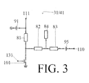
- FIG. 3 depicts the output 31, 41 of either the receive amplifier 30 or the transmit amplifier 40, which may be operated according to an embodiment of the present invention.
- the output 31, 41 of the amplifier 30, 40 includes tuning elements 81, 82, 83, and 84, wherein harmonic tuning of the amplifier 30, 40 may be achieved using tuning elements 81 and 84.
- the tuning elements 82, 83, and 84 may be operated as a quarter-wave shunt switch.
- the output 31, 41 also includes capacitors 91 and 95, wherein capacitor 95 may achieve the operation of the combination of capacitors 93 and 94 shown in FIG. 2 .
- the output 31, 41 also includes amplifier transistor 101 that may be manipulated along with a drain voltage 111 and the tuning elements 81, 82, 83, and 84 to control the impedance of the amplifier output 31, 41.
- the amplifier transistor 101 may be an FET, although the present invention is not limited thereto.
- the impedance of line 110 is a nominal impedance, such as, for example, 50 ohms.
- the impedance of line 110 is high, e.g., an "open-circuit" impedance, and electrical signals along the receive path are effectively blocked by the receive amplifier 30.
- the impedance of line 110 of the transmit amplifier 40 is a nominal impedance, allowing an electrical signal to pass therethrough.
- the impedance of line 110 of the transmit amplifier 40 is high, and electrical signals along the transmit path are effectively blocked by the transmit amplifier 40.
- the amplifier transistor 101 may be operated by delivering a gate signal from a system processor 100 to the gate of the amplifier transistor 101 via a gate signal line 131, and by also manipulating the drain voltage of line 111 by operation of the system processor 100.
- the gate signal delivered to the gate of the amplifier transistor 101 may depend on the operation of the switch transistor 102, shown in FIG. 2 .
- the functions of transistors 101 and 102 of FIG. 2 may be combined, and the amplifier transistor 101 may be operated as an RF switch.
- harmonic tuning may be achieved by harmonically tuning the tuning elements 81 and 84 via transmission lines.
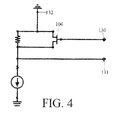
- FIG. 4 depicts a method of bias modification of an amplifier 30, 40 according to an embodiment of the present invention.
- the TR state line 130 may control a bias modification transistor 106 by using a control voltage signal, such as the TR control signal, to turn the bias modification transistor 106 on or off.
- the bias modification transistor 106 may be an FET, and may also be the switch transistor 102, although the present invention is not limited thereto.
- the gate signal line 131 is electrically coupled to ground 132. This in turn grounds out the gate of the of the gate transistor 101 of the amplifier 30, 40 shown in FIG. 3 .
- the drain voltage 111 at the output side 31/41 of the amplifier 30/40 must be approximately 0 volts. Accordingly, by manipulating the bias voltage of the bias transistor 106, the impedance of the amplifier 30, 40, may be controlled, and the amplifier 30, 40 may be operated as a switch.
- an amplifier in an electrical system is operated as a switch.
- operation of an amplifier 30, 40 according to embodiments of the present invention is depicted in conjunction with a TR system 10
- operation of an amplifier 30, 40 according to other embodiments may apply to other situations wherein a path through the amplifier is to be opened and closed.
- embodiments of the present invention may be applied to a single amplifier whose output is employed as a signal switch in the absence of an antenna or other components of a TR system, such as a system processor.
- embodiments of the present invention may be applied to an antenna system lacking bidirectional capability (e.g., operating in either a receive mode or a transmit mode), wherein an output of an amplifier is employed as a signal switch in a signal path (e.g., transmit or receive) of the antenna system.
Landscapes
- Engineering & Computer Science (AREA)
- Power Engineering (AREA)
- Amplifiers (AREA)
Applications Claiming Priority (1)
| Application Number | Priority Date | Filing Date | Title |
|---|---|---|---|
| US13/149,640 US20120306578A1 (en) | 2011-05-31 | 2011-05-31 | Rf amplifier with open circuit output off-state |
Publications (2)
| Publication Number | Publication Date |
|---|---|
| EP2530833A2 true EP2530833A2 (de) | 2012-12-05 |
| EP2530833A3 EP2530833A3 (de) | 2013-09-11 |
Family
ID=46026646
Family Applications (1)
| Application Number | Title | Priority Date | Filing Date |
|---|---|---|---|
| EP12163913.2A Withdrawn EP2530833A3 (de) | 2011-05-31 | 2012-04-12 | HF-Verstärker mit offenem Schaltungsausgang im Aus-Zustand |
Country Status (2)
| Country | Link |
|---|---|
| US (1) | US20120306578A1 (de) |
| EP (1) | EP2530833A3 (de) |
Families Citing this family (2)
| Publication number | Priority date | Publication date | Assignee | Title |
|---|---|---|---|---|
| GB202011276D0 (en) * | 2020-07-21 | 2020-09-02 | Sofant Tech Ltd | Phased array antenna apparatus and method |
| EP4454125A4 (de) | 2021-12-22 | 2025-12-03 | Reach Power Inc | Bidirektionale hf-schaltung und verfahren zur verwendung |
Family Cites Families (5)
| Publication number | Priority date | Publication date | Assignee | Title |
|---|---|---|---|---|
| US4637073A (en) * | 1984-06-25 | 1987-01-13 | Raytheon Company | Transmit/receive switch |
| JP3037850B2 (ja) * | 1993-04-30 | 2000-05-08 | アルプス電気株式会社 | 高周波増幅器 |
| US7110742B2 (en) * | 2004-03-16 | 2006-09-19 | Broadcom Corporation | Low noise amplifier with constant input impedance |
| US7167044B2 (en) * | 2004-05-10 | 2007-01-23 | University Of Florida Research Foundation, Inc. | Dual-band CMOS front-end with two gain modes |
| US7486135B2 (en) * | 2007-05-29 | 2009-02-03 | Telefonaktiebolaget Lm Ericsson (Publ) | Configurable, variable gain LNA for multi-band RF receiver |
-
2011
- 2011-05-31 US US13/149,640 patent/US20120306578A1/en not_active Abandoned
-
2012
- 2012-04-12 EP EP12163913.2A patent/EP2530833A3/de not_active Withdrawn
Non-Patent Citations (1)
| Title |
|---|
| None |
Also Published As
| Publication number | Publication date |
|---|---|
| US20120306578A1 (en) | 2012-12-06 |
| EP2530833A3 (de) | 2013-09-11 |
Similar Documents
| Publication | Publication Date | Title |
|---|---|---|
| KR102287445B1 (ko) | 저잡음 증폭기를 바이패스하는 시스템 및 방법 | |
| US8271028B2 (en) | Dual band amplifier | |
| US8044540B2 (en) | Systems and methods for a SPDT switch or SPMT switch with transformer | |
| EP2847869B1 (de) | Sender-empfänger mit integriertem konfigurierbarem rx/tx-passivnetzwerk | |
| US20250167824A1 (en) | Hybrid coupler based t/r switch | |
| JPH08335801A (ja) | 電子制御装置 | |
| US10848197B2 (en) | Hybrid coupler based T/R switch | |
| US9107240B2 (en) | Amplifier supporting multi mode and amplifying method thereof | |
| US20190334572A1 (en) | Radio-frequency transceiver front-end circuit | |
| US20060009164A1 (en) | Radio frequency switching circuit | |
| US8437723B2 (en) | Amplifier circuit and communication device | |
| US20190123778A1 (en) | Monolithic microwave integrated circuit (mmic) for phased array antenna system and phased array antenna system including the same | |
| US9899968B2 (en) | Low noise amplifier circuit | |
| US6667670B2 (en) | Microwave double-pole double-throw switch and microwave divide/through switch and power amplifier using thereof | |
| US7420424B2 (en) | Power amplifier transmission line transformer | |
| EP2530833A2 (de) | HF-Verstärker mit offenem Schaltungsausgang im Aus-Zustand | |
| JP2016158216A (ja) | 高周波半導体集積回路 | |
| CN110572143B (zh) | 具有高线性度的单刀双掷(spdt)开关和发送-接收电路 | |
| KR20110017639A (ko) | 공핍 모드 고전자 이동도 트랜지스터를 포함하는 전력 증폭기 | |
| JP2004007703A (ja) | 非対称、電圧最適化、広帯域共通ゲート双方向mmic増幅器 | |
| EP2530834A1 (de) | RF-Verstärker mit offener Leitungs-Eingabe-Ausstatus | |
| JP5161856B2 (ja) | バイアス回路 | |
| US12149208B2 (en) | Electronic circuit and power amplifier comprising same | |
| KR101567472B1 (ko) | 송수신 스위치가 없는 양방향 증폭장치 | |
| US20040229573A1 (en) | Amplification device with shared amplification stage for transmission and reception |
Legal Events
| Date | Code | Title | Description |
|---|---|---|---|
| PUAI | Public reference made under article 153(3) epc to a published international application that has entered the european phase |
Free format text: ORIGINAL CODE: 0009012 |
|
| 17P | Request for examination filed |
Effective date: 20120507 |
|
| AK | Designated contracting states |
Kind code of ref document: A2 Designated state(s): AL AT BE BG CH CY CZ DE DK EE ES FI FR GB GR HR HU IE IS IT LI LT LU LV MC MK MT NL NO PL PT RO RS SE SI SK SM TR |
|
| AX | Request for extension of the european patent |
Extension state: BA ME |
|
| PUAL | Search report despatched |
Free format text: ORIGINAL CODE: 0009013 |
|
| STAA | Information on the status of an ep patent application or granted ep patent |
Free format text: STATUS: THE APPLICATION HAS BEEN WITHDRAWN |
|
| AK | Designated contracting states |
Kind code of ref document: A3 Designated state(s): AL AT BE BG CH CY CZ DE DK EE ES FI FR GB GR HR HU IE IS IT LI LT LU LV MC MK MT NL NO PL PT RO RS SE SI SK SM TR |
|
| AX | Request for extension of the european patent |
Extension state: BA ME |
|
| RIC1 | Information provided on ipc code assigned before grant |
Ipc: H03F 3/60 20060101ALI20130807BHEP Ipc: H03F 3/72 20060101ALI20130807BHEP Ipc: H03F 3/193 20060101ALI20130807BHEP Ipc: H03F 3/24 20060101ALI20130807BHEP Ipc: H03F 1/56 20060101AFI20130807BHEP |
|
| 18W | Application withdrawn |
Effective date: 20130827 |