EP2528215A2 - Ausgleich der Temperaturen in einem Mehrphasen-Gleichsstromumrichter - Google Patents
Ausgleich der Temperaturen in einem Mehrphasen-Gleichsstromumrichter Download PDFInfo
- Publication number
- EP2528215A2 EP2528215A2 EP12169479A EP12169479A EP2528215A2 EP 2528215 A2 EP2528215 A2 EP 2528215A2 EP 12169479 A EP12169479 A EP 12169479A EP 12169479 A EP12169479 A EP 12169479A EP 2528215 A2 EP2528215 A2 EP 2528215A2
- Authority
- EP
- European Patent Office
- Prior art keywords
- phased
- signal
- circuit
- current
- temperature
- Prior art date
- Legal status (The legal status is an assumption and is not a legal conclusion. Google has not performed a legal analysis and makes no representation as to the accuracy of the status listed.)
- Granted
Links
Images

Classifications
-
- H—ELECTRICITY
- H02—GENERATION; CONVERSION OR DISTRIBUTION OF ELECTRIC POWER
- H02M—APPARATUS FOR CONVERSION BETWEEN AC AND AC, BETWEEN AC AND DC, OR BETWEEN DC AND DC, AND FOR USE WITH MAINS OR SIMILAR POWER SUPPLY SYSTEMS; CONVERSION OF DC OR AC INPUT POWER INTO SURGE OUTPUT POWER; CONTROL OR REGULATION THEREOF
- H02M3/00—Conversion of DC power input into DC power output
- H02M3/02—Conversion of DC power input into DC power output without intermediate conversion into AC
- H02M3/04—Conversion of DC power input into DC power output without intermediate conversion into AC by static converters
- H02M3/10—Conversion of DC power input into DC power output without intermediate conversion into AC by static converters using discharge tubes with control electrode or semiconductor devices with control electrode
- H02M3/145—Conversion of DC power input into DC power output without intermediate conversion into AC by static converters using discharge tubes with control electrode or semiconductor devices with control electrode using devices of a triode or transistor type requiring continuous application of a control signal
- H02M3/155—Conversion of DC power input into DC power output without intermediate conversion into AC by static converters using discharge tubes with control electrode or semiconductor devices with control electrode using devices of a triode or transistor type requiring continuous application of a control signal using semiconductor devices only
- H02M3/156—Conversion of DC power input into DC power output without intermediate conversion into AC by static converters using discharge tubes with control electrode or semiconductor devices with control electrode using devices of a triode or transistor type requiring continuous application of a control signal using semiconductor devices only with automatic control of output voltage or current, e.g. switching regulators
- H02M3/158—Conversion of DC power input into DC power output without intermediate conversion into AC by static converters using discharge tubes with control electrode or semiconductor devices with control electrode using devices of a triode or transistor type requiring continuous application of a control signal using semiconductor devices only with automatic control of output voltage or current, e.g. switching regulators including plural semiconductor devices as final control devices for a single load
- H02M3/1584—Conversion of DC power input into DC power output without intermediate conversion into AC by static converters using discharge tubes with control electrode or semiconductor devices with control electrode using devices of a triode or transistor type requiring continuous application of a control signal using semiconductor devices only with automatic control of output voltage or current, e.g. switching regulators including plural semiconductor devices as final control devices for a single load with a plurality of power processing stages connected in parallel
-
- H—ELECTRICITY
- H02—GENERATION; CONVERSION OR DISTRIBUTION OF ELECTRIC POWER
- H02M—APPARATUS FOR CONVERSION BETWEEN AC AND AC, BETWEEN AC AND DC, OR BETWEEN DC AND DC, AND FOR USE WITH MAINS OR SIMILAR POWER SUPPLY SYSTEMS; CONVERSION OF DC OR AC INPUT POWER INTO SURGE OUTPUT POWER; CONTROL OR REGULATION THEREOF
- H02M1/00—Details of apparatus for conversion
- H02M1/0003—Details of control, feedback or regulation circuits
-
- H—ELECTRICITY
- H02—GENERATION; CONVERSION OR DISTRIBUTION OF ELECTRIC POWER
- H02M—APPARATUS FOR CONVERSION BETWEEN AC AND AC, BETWEEN AC AND DC, OR BETWEEN DC AND DC, AND FOR USE WITH MAINS OR SIMILAR POWER SUPPLY SYSTEMS; CONVERSION OF DC OR AC INPUT POWER INTO SURGE OUTPUT POWER; CONTROL OR REGULATION THEREOF
- H02M1/00—Details of apparatus for conversion
- H02M1/32—Means for protecting converters other than automatic disconnection
- H02M1/327—Means for protecting converters other than automatic disconnection against abnormal temperatures
Definitions
- This invention relates to multi-phase DC/DC converters and, in particular, to the thermal control of each phase of the converter.
- Multi-phase DC/DC converters are generally used for high current applications, such as for generating a load current of 100A or more.
- Employing multiple phases of the converter allows a sharing of the current generation, lowers ripple, and achieves other well known benefits.
- each phase generally comprises a pulse width modulation (PWM) comparator, an RS flip flop for turning a transistor switch on and off at a certain duty cycle to achieve regulation, an inductor, and a current sense device such as a low value resistor.
- PWM pulse width modulation
- the turn-on time for each phase is controlled by a phased clock.
- a switch turns on, a ramping current flows through its associated inductor.
- the phased ramping currents through the inductors are filtered by an output capacitor common to all phases.
- An error amplifier compares the output voltage of the converter to a reference voltage and generates a control voltage whose level corresponds to the duty cycle of the phases needed to maintain the output voltage at the desired voltage.
- the PMW comparator for each phase then compares the control voltage level to the current ramp through the inductor. When they cross, the RS flip flop controls the switch to turn off. In this manner, ideally, each phase is controlled to have the same duty cycle and contributes an equal amount of current to the load.
- the temperatures of the various phases are slightly different due to at least the following factors: 1) the different physical positions of the various phases on a circuit board; 2) unequal cooling of the phases by forced air flow and heat sinking; and 3) non-matching components.
- This difference in operating temperatures causes the electrical characteristics of the phases (e.g., the on-resistances of MOSFET switches, the inductances, the current sense resistances, etc.) to be affected differently, resulting in non-matching currents being supplied at the same duty cycles and increased ripple.
- Such temperature imbalances may also result in "hot spots" that reduce the reliability and performance of the system.
- This problem applies to all types of multi-phase DC/DC converters that use a sensed current in the feedback loop for regulation.
- a thermal compensation circuit is provided for each phase of a multi-phase DC/DC converter.
- Each compensation circuit has a temperature sensor that is used to generate a "first signal" for each phase corresponding to the temperature of that phase.
- the temperature may represent the temperature of the inductor or MOSFET switch for that phase, since those components conduct the full average current for that phase. An increased average current increases the temperature of those components.
- a "third signal” is generated corresponding to the difference between the "first signal” and the "second signal.”
- the "third signal” for each phase is then used to separately adjust the duty cycle of each phase to control the temperature of each phase to be substantially equal to the average temperature (i.e., cause the "first signal” to equal the "second signal” for each phase).
- Some duty cycles may be increased while other duty cycles may be decreased until a steady state condition is reached. Accordingly, the temperatures of the phases will be balanced. As a result, the output voltage of the converter should be more optimally regulated during steady state operation, with lower ripple due to the improved matching of performance of the phases.
- the duty cycles are adjusted by the thermal compensation circuits effectively offsetting the control voltage applied to each PWM comparator in each phase.
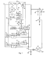
- Fig. 1 illustrates one type of multi-phase DC/DC converter using thermal compensation, in accordance with one embodiment of the present invention. Many other types of multi-phase converters can also benefit from the present invention.
- the particular type of converter shown is a peak current-mode controlled converter.
- phase 1-phase 3 Three phases (phase 1-phase 3) are shown in Fig. 1 , although the invention may be applied to any number of phases. Only the components in phase 1 are shown for simplicity.
- a clock (Clk) signal for each phase is applied to the set input of an RS flip flop 20. Each Clk signal is phase-delayed relative to the other by a delay circuit 22.
- the setting of the RS flip flop 20 generates a high signal at its Q output.
- the logic circuit 24 ensures that there is no cross-conduction.
- the input voltage Vin coupled to an inductor 30 through the switch 26 causes a ramping current to flow through the inductor 30, and this current flows through a low value sense resistor 32.
- the ramping current is filtered by an output capacitor 36 and supplies current to the load.
- the output capacitor 36 is shared by all phases and smoothes out ripple.
- the output voltage Vo is applied to a voltage divider 42, and the divided voltage is applied to an input of a transconductance amplifier 44.
- a reference voltage Vref is applied to the other input of the amplifier 44.
- the output current of the amplifier 44 corresponds to the difference between the actual output voltage and the desired output voltage.
- the voltage (a control voltage Vc) across a capacitor 46 at the output of the amplifier 44 is adjusted up or down based on the positive or negative current output of the amplifier 44. Since the control voltage Vc at the capacitor 46, among other things, sets the duty cycles of the phases, the level of the control voltage Vc is that needed to equalize the inputs into the amplifier 44.
- the control voltage Vc is applied to a PWM comparator 50.
- the voltage across the sense resistor 32 is sensed by a differential amplifier 52, having a certain gain, and, when the ramped current through the sense resistor 32 exceeds the control voltage Vc, the PWM comparator 50 is triggered to output a reset signal to the RS flip flop 20.
- This turns the charging switch 26 off and turns the synchronous rectifier switch 28 on to discharge the inductor 30, causing a downward ramping current. In this way, the peak current through the inductor 30 for each phase is regulated to cause a desired output voltage Vo.
- the duty cycles of the three phases are identical irrespective of the different temperatures of the three phases. Accordingly, the electrical characteristics of the three phases, which fluctuate with temperature, will be different, resulting in unmatched currents provided by the phases. This leads to various problems such as increased ripple and over-current issues.
- the present invention changes the above-described conventional operation by adjusting the duty cycles of the phases so that the temperatures are matched, while the converter still outputs the desired regulated voltage.
- the thermal compensation control signal (TCC1, TCC2, TCC3) for each of the three phases offsets the control voltage Vc up or down for each of the three phases to change the duty cycles of the phases until the measured temperatures of the three phases are equal.
- the duty cycles can be controlled in other ways, also envisioned by the present invention, such as offsetting the current sense signal or adjusting any other suitable signal in the feedback path.
- the control voltage Vc is converted into a corresponding current at each of the phases by the Vc to Ic converter circuit 56, using any of a number of well known techniques.
- a derived TCC signal (TCC1, TCC2, TCC3) is then applied to each Ic signal to add current or subtract current, shown as the Ic offset circuit 57 (which may simply be a node).
- the resulting currents (Ic1, Ic2, Ic3) are then converted back into control voltages (e.g., Vc1) by a resistor 58, assuming the PWM comparator 50 has a suitably high input impedance.
- the current offsets are those needed to cause the measured temperatures of the phases to be matched, irrespective of the relative duty cycles.
- Fig. 1 also illustrates a conventional slope compensation circuit 59, as is well known.
- the slope compensation circuit 59 turns off the switch 26 before the inductor current ramp crosses the control voltage Vc to reduce subharmonic oscillations that may occur at the high duty cycles.
- the effect of the slope compensation circuit 59 is unrelated to the present invention.
- Fig. 2 illustrates one type of thermal compensation circuit that can be used to generate the TCC 1-TCC 3 signals and the average temperature signal Tavg.
- the temperature compensation circuits for the phases are substantially identical. Only two compensation circuits are shown in Fig. 2 for simplicity.
- a current source 70 generates a current through a temperature sensor 72 to create a first signal at the pin Tcomp1.
- the sensor 72 may be a negative temperature coefficient (NTC) resistor connected to ground.
- NTC negative temperature coefficient
- the temperature sensor may comprise a pn junction and related circuitry, where the known effect of temperature on the conductance of a pn junction is converted into a corresponding signal. Temperature sensor ICs are commercially available and may also be used.
- the current source 70 is trimmed, such as by blowing fuses during fabrication, so that the signals at pins Tcomp1 and Tcomp2 are identical when the sensors 72 are at the same temperature.
- the voltage signals at the Tcomp2 and Tcomp2 pins are converted into corresponding currents by the voltage-to-current conversion circuit formed by a differential amplifier 74, MOSFET 76, and resistor 78.
- the current through the resistor 78 is that needed to cause the resulting voltage across it to equal the signal at the Tcomp1 pin (equalizing the voltages at the inputs of the differential amplifier 74).
- the same voltage-to-current converter technique may be used in the Vc to Ic converter circuits 56 in Fig. 1 to convert the control voltage Vc to the current Ic.
- a conventional current mirror circuit 80 generates the same or a scaled current at an output 82.
- the current mirror circuits 80 for the various phases are trimmed during fabrication so that their outputs are the same when the temperature sensors 72 are at the same temperatures.
- the currents output by the current mirror circuits 80 for the various phases are summed at node 84, and the summed currents flow through the resistor 86.
- the resulting voltage at the pin Tavg corresponds to the average temperature for all of the phases.
- the value of the resistor 86 is selected such that the level of the voltage at the pin Tavg is equal to the level of the voltage at the Tcomp2 and Tcomp2 pins when the temperatures of the sensors 72 are equal (i.e., when each sensor 72 senses the average temperature)
- the capacitor 88 is a smoothing capacitor to prevent perturbations.
- the signal at the Tcomp2 pin and the signal at the Tavg pin are applied to a transconductance amplifier 90, which converts the difference into a corresponding positive or negative current.
- the capacitor 92 is relatively small and is used for noise filtering.
- the currents generated by the transconductance amplifiers 90 are used to offset the Ic signals generated at each phase in Fig. 2 . Therefore, the thermal compensation circuits will offset Ic for each phase to cause the inputs at the transconductance amplifier 90 ( Fig. 2 ) to substantially match.
- Higher duty cycles increase the average currents in a phase, and an increase in the average current will raise the temperature of the inductor and switch for that phase.
- the thermal compensation circuit will subtract current from the Ic signal to reduce the duty cycle of that phase to lower its temperature. This will, in turn, affect the output voltage Vo and the average temperature, so the control voltage Vc and the duty cycles of the other phases will be affected.
- a steady state will be reached where the output voltage is at the desired voltage and the duty cycles of the various phases are adjusted so that the sensed temperatures of the phases are equal.
- the time constant of the thermal compensation feedback loop is relatively long to avoid oscillations.
- the DC/DC converters use synchronous rectifier MOSFETs, it is preferable to locate the temperature sensors 72 proximate to those MOSFETs.
- Some MOSFET modules are formed with an integral thermal sensor. Alternatively, the temperature of the inductor or the topside power switch can be measured.
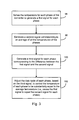
- Fig. 3 is a flowchart of the thermal compensation process.
- step 96 the temperature for each phase in the converter is sensed to generate corresponding first signals for all the phases.
- step 98 the first signals are averaged to generate a second signal.
- step 100 for each phase, a third signal is generated for each phase corresponding to the difference between the first signal and the second signal.
- step 102 the third signal is then used to adjust the duty cycle of each phase to control the temperature of each phase to be substantially equal to the average temperature (i.e., cause the first signal to equal the second signal for each phase). Some duty cycles may be increased while other duty cycles may be decreased. In the steady state, the output voltage of the converter will be the desired voltage and the temperatures of the phases will be balanced.
- multiple converter phases are formed on a single chip housed in a surface mounted package with pins for externally connected inductors, transistor switches, and capacitors.
- the temperature sensor may be an external sensor mounted proximate to the inductor or switch on a circuit board.
- the remainder of the thermal compensation circuit (for all phases) may be formed as a single chip or in the converter chip itself. This allows the components in the thermal compensation circuits to be easily trimmed so that the compensation circuits for the phases are substantially identical.
- the thermal compensation circuits may be formed as a separate product to be used with any type of DC/DC converter.
Landscapes
- Engineering & Computer Science (AREA)
- Power Engineering (AREA)
- Dc-Dc Converters (AREA)
Applications Claiming Priority (1)
| Application Number | Priority Date | Filing Date | Title |
|---|---|---|---|
| US13/115,924 US8587272B2 (en) | 2011-05-25 | 2011-05-25 | Balancing temperatures in a multi-phase DC/DC converter |
Publications (3)
| Publication Number | Publication Date |
|---|---|
| EP2528215A2 true EP2528215A2 (de) | 2012-11-28 |
| EP2528215A3 EP2528215A3 (de) | 2014-08-06 |
| EP2528215B1 EP2528215B1 (de) | 2017-01-11 |
Family
ID=46147353
Family Applications (1)
| Application Number | Title | Priority Date | Filing Date |
|---|---|---|---|
| EP12169479.8A Not-in-force EP2528215B1 (de) | 2011-05-25 | 2012-05-25 | Ausgleich der Temperaturen in einem Mehrphasen-Gleichsstromumrichter |
Country Status (3)
| Country | Link |
|---|---|
| US (1) | US8587272B2 (de) |
| EP (1) | EP2528215B1 (de) |
| CN (1) | CN102810981B (de) |
Cited By (2)
| Publication number | Priority date | Publication date | Assignee | Title |
|---|---|---|---|---|
| GB2517475A (en) * | 2013-08-22 | 2015-02-25 | Utilitywise Plc | Voltage regulator |
| EP2884653A1 (de) * | 2013-12-12 | 2015-06-17 | Alstom Technology Ltd | Verbesserungen an oder im Zusammenhang mit der Steuerung von Wandlern |
Families Citing this family (19)
| Publication number | Priority date | Publication date | Assignee | Title |
|---|---|---|---|---|
| US20120249101A1 (en) * | 2011-04-01 | 2012-10-04 | Akey David W | Consistently balanced thermal load dc-dc converter |
| US9780665B2 (en) * | 2012-03-15 | 2017-10-03 | GM Global Technology Operations LLC | Methods and systems for controlling a boost converter |
| CN103296867B (zh) * | 2013-06-28 | 2015-07-15 | 成都芯源系统有限公司 | 多相开关变换器及其控制器和控制方法 |
| DE102013113012A1 (de) * | 2013-11-25 | 2015-05-28 | Weidmüller Interface GmbH & Co. KG | Schaltnetzteil und Verfahren zum Regeln einer Ausgangsspannung eines Schaltnetzteils |
| US9455619B1 (en) * | 2013-11-26 | 2016-09-27 | Lockheed Martin Corporation | System and method for implementing current sharing between packaged power supplies |
| JP6279898B2 (ja) * | 2013-12-26 | 2018-02-14 | 株式会社東芝 | スイッチング制御装置 |
| DE102015100023A1 (de) * | 2015-01-05 | 2016-07-07 | Hella Kgaa Hueck & Co. | Schaltungsanordnung zum zumindest abschnittsweise Nachbilden eines magnetischen Flusses durch Induktivitäten eines Gleichspannungswandlers mit mehreren Phasen |
| DE102015100022A1 (de) * | 2015-01-05 | 2016-07-07 | Hella Kgaa Hueck & Co. | Schaltungsanordnung zum zumindest abschnittsweise Nachbilden eines magnetischen Flusses durch zumindest zwei Induktivitäten eines mehrphasigen Gleichspannungswandlers |
| KR101717761B1 (ko) * | 2015-06-18 | 2017-03-22 | (주)티에이치엔 | 차량용 이중 전원 시스템 |
| KR102490603B1 (ko) * | 2015-09-24 | 2023-01-19 | 현대모비스 주식회사 | 하이브리드 전기차량 시스템의 컨버터 |
| US10099787B2 (en) | 2016-01-22 | 2018-10-16 | B/E Aerospace, Inc. | Method and apparatus for correcting for power harmonics |
| JP2017225227A (ja) * | 2016-06-14 | 2017-12-21 | 住友電気工業株式会社 | 電源装置及びコンピュータプログラム |
| US10637353B2 (en) * | 2016-11-30 | 2020-04-28 | Dialog Semiconductor (Uk) Limited | Feedback voltage DC level cancelling for configurable output DC-DC switching converters |
| TWI781995B (zh) * | 2017-03-22 | 2022-11-01 | 美商瑞薩電子美國有限公司 | 在多相電壓調節器中組合溫度監測和真實的不同電流感測 |
| CN108183612B (zh) * | 2018-03-13 | 2024-06-21 | 北京比特大陆科技有限公司 | 可扩展的并联供电dc-dc电源装置 |
| CN111966204B (zh) * | 2020-07-29 | 2022-05-31 | 苏州浪潮智能科技有限公司 | 一种温度监控方法、电路、设备及存储介质 |
| JP7405041B2 (ja) * | 2020-08-25 | 2023-12-26 | Tdk株式会社 | コンバータ装置および電源装置 |
| WO2024154487A1 (ja) * | 2023-01-20 | 2024-07-25 | ローム株式会社 | 電源制御装置、スイッチング電源 |
| EP4657727A1 (de) * | 2024-05-29 | 2025-12-03 | Airbus Defence and Space GmbH | Mehrphasiger abwärtswandler |
Family Cites Families (8)
| Publication number | Priority date | Publication date | Assignee | Title |
|---|---|---|---|---|
| US6292378B1 (en) * | 2000-04-07 | 2001-09-18 | Linfinity Microelectronics | Method and apparatus for programmable current sharing |
| US6449174B1 (en) * | 2001-08-06 | 2002-09-10 | Fairchild Semiconductor Corporation | Current sharing in a multi-phase power supply by phase temperature control |
| US7262628B2 (en) * | 2004-07-02 | 2007-08-28 | Primarion, Inc. | Digital calibration with lossless current sensing in a multiphase switched power converter |
| US6806689B2 (en) * | 2002-03-22 | 2004-10-19 | International Rectifier Corporation | Multi-phase buck converter |
| JP2007527685A (ja) * | 2003-06-30 | 2007-09-27 | ニューパワー・セミコンダクター・インコーポレイテッド | 電源電流検出および垂下損失補償のためのプログラマブル較正回路 |
| US7615982B1 (en) * | 2006-07-26 | 2009-11-10 | Fairchild Semiconductor Corporation | Power converter able to rapidly respond to fast changes in load current |
| WO2009010476A1 (en) * | 2007-07-13 | 2009-01-22 | Powervation Limited | A power converter |
| TWI414932B (zh) * | 2009-11-19 | 2013-11-11 | Asustek Comp Inc | 多相位電源供應裝置與其電流調整方法 |
-
2011
- 2011-05-25 US US13/115,924 patent/US8587272B2/en not_active Expired - Fee Related
-
2012
- 2012-05-25 EP EP12169479.8A patent/EP2528215B1/de not_active Not-in-force
- 2012-05-25 CN CN201210166865.6A patent/CN102810981B/zh active Active
Cited By (7)
| Publication number | Priority date | Publication date | Assignee | Title |
|---|---|---|---|---|
| GB2517475A (en) * | 2013-08-22 | 2015-02-25 | Utilitywise Plc | Voltage regulator |
| EP2884653A1 (de) * | 2013-12-12 | 2015-06-17 | Alstom Technology Ltd | Verbesserungen an oder im Zusammenhang mit der Steuerung von Wandlern |
| WO2015086837A1 (en) * | 2013-12-12 | 2015-06-18 | Alstom Technology Ltd | Improvements in or relating to converters for use in high voltage direct current power transmission |
| WO2015086844A1 (en) * | 2013-12-12 | 2015-06-18 | Alstom Technology Ltd | Improvements in or relating to the control of converters |
| WO2015086842A1 (en) * | 2013-12-12 | 2015-06-18 | Alstom Technology Ltd | Improvements in or relating to converters for use in high voltage direct current power transmission |
| CN105981287A (zh) * | 2013-12-12 | 2016-09-28 | 通用电气技术有限公司 | 变换器控制的改进或与变换器控制有关的改进 |
| US10027217B2 (en) | 2013-12-12 | 2018-07-17 | General Electric Technology Gmbh | Converter and method of controlling a converter |
Also Published As
| Publication number | Publication date |
|---|---|
| US20120299560A1 (en) | 2012-11-29 |
| EP2528215A3 (de) | 2014-08-06 |
| EP2528215B1 (de) | 2017-01-11 |
| US8587272B2 (en) | 2013-11-19 |
| CN102810981A (zh) | 2012-12-05 |
| CN102810981B (zh) | 2015-05-06 |
Similar Documents
| Publication | Publication Date | Title |
|---|---|---|
| US8587272B2 (en) | Balancing temperatures in a multi-phase DC/DC converter | |
| US10554127B2 (en) | Control circuit and control method for multi-output DC-DC converter | |
| US9793800B1 (en) | Multiphase switching power supply with robust current sensing and shared amplifier | |
| TWI458217B (zh) | 電流平衡電路及其多相位直流至直流轉換器與電流平衡方法 | |
| US7208921B2 (en) | DC-DC regulator with switching frequency responsive to load | |
| US9831781B2 (en) | Fast transient power supply with a separated high frequency and low frequency path signals | |
| KR101840412B1 (ko) | 벅 스위치 모드 파워 컨버터 큰 신호 천이 응답 최적화기 | |
| US10256727B2 (en) | Multi-phase power supply with DC-DC converter integrated circuits having current sharing function | |
| US20200021189A1 (en) | Current balance method used in multi-phase switching converters | |
| TWI393332B (zh) | 升降轉換電路的控制電路以及控制方法 | |
| Duan et al. | Current-mode variable-frequency control architecture for high-current low-voltage DC–DC converters | |
| Hu et al. | A Fixed-Frequency Quasi-${\rm V}^{2} $ Hysteretic Buck Converter With PLL-Based Two-Stage Adaptive Window Control | |
| US9568376B2 (en) | Temperature detecting circuit and method thereof | |
| US12206320B2 (en) | Adaptive inductor DCR current sensing circuit in a switching converter and associated method | |
| Yuan et al. | Hybrid buck converter with constant mode changing point and smooth mode transition for high-frequency applications | |
| CN105099188A (zh) | Dc-dc变换器 | |
| CN111758211A (zh) | 包括输入控制元件的电压转换器布置及操作电压转换器布置的方法 | |
| TWI539730B (zh) | 切換模式電力供應器之效率最佳化、經校準無感測器之電力/能量轉換 | |
| Cho et al. | A 1.23 W/mm 2 83.7%-Efficiency 400MHz 6-Phase Fully Integrated Buck Converter in 28nm CMOS with On-Chip Capacitor Dynamic Re-Allocation for Inter-Inductor Current Balancing and Fast DVS of 75mV/ns | |
| Lin et al. | Digital multiphase buck converter with current balance/phase shedding control | |
| JP6912300B2 (ja) | スイッチングレギュレータ | |
| Su et al. | Pseudo-ramp current balance (PRCB) technique with offset cancellation control (OCC) in dual-phase DC-DC buck converter | |
| US9705412B2 (en) | Pulsed feedback switching converter | |
| US11081957B2 (en) | Power converter with multi-mode timing control | |
| US20230223851A1 (en) | Apparatus and method for controlling transient boost circuit of voltage regulator through feedback signals obtained by differential sensing applied to output capacitor |
Legal Events
| Date | Code | Title | Description |
|---|---|---|---|
| PUAI | Public reference made under article 153(3) epc to a published international application that has entered the european phase |
Free format text: ORIGINAL CODE: 0009012 |
|
| AK | Designated contracting states |
Kind code of ref document: A2 Designated state(s): AL AT BE BG CH CY CZ DE DK EE ES FI FR GB GR HR HU IE IS IT LI LT LU LV MC MK MT NL NO PL PT RO RS SE SI SK SM TR |
|
| AX | Request for extension of the european patent |
Extension state: BA ME |
|
| REG | Reference to a national code |
Ref country code: DE Ref legal event code: R079 Ref document number: 602012027636 Country of ref document: DE Free format text: PREVIOUS MAIN CLASS: H02M0003000000 Ipc: H02M0003158000 |
|
| PUAL | Search report despatched |
Free format text: ORIGINAL CODE: 0009013 |
|
| AK | Designated contracting states |
Kind code of ref document: A3 Designated state(s): AL AT BE BG CH CY CZ DE DK EE ES FI FR GB GR HR HU IE IS IT LI LT LU LV MC MK MT NL NO PL PT RO RS SE SI SK SM TR |
|
| AX | Request for extension of the european patent |
Extension state: BA ME |
|
| RIC1 | Information provided on ipc code assigned before grant |
Ipc: H02M 1/32 20070101ALI20140630BHEP Ipc: H02M 3/158 20060101AFI20140630BHEP Ipc: H02M 1/00 20070101ALI20140630BHEP |
|
| 17P | Request for examination filed |
Effective date: 20150129 |
|
| RBV | Designated contracting states (corrected) |
Designated state(s): AL AT BE BG CH CY CZ DE DK EE ES FI FR GB GR HR HU IE IS IT LI LT LU LV MC MK MT NL NO PL PT RO RS SE SI SK SM TR |
|
| 17Q | First examination report despatched |
Effective date: 20150512 |
|
| GRAP | Despatch of communication of intention to grant a patent |
Free format text: ORIGINAL CODE: EPIDOSNIGR1 |
|
| INTG | Intention to grant announced |
Effective date: 20160729 |
|
| STAA | Information on the status of an ep patent application or granted ep patent |
Free format text: STATUS: GRANT OF PATENT IS INTENDED |
|
| GRAS | Grant fee paid |
Free format text: ORIGINAL CODE: EPIDOSNIGR3 |
|
| GRAA | (expected) grant |
Free format text: ORIGINAL CODE: 0009210 |
|
| STAA | Information on the status of an ep patent application or granted ep patent |
Free format text: STATUS: THE PATENT HAS BEEN GRANTED |
|
| AK | Designated contracting states |
Kind code of ref document: B1 Designated state(s): AL AT BE BG CH CY CZ DE DK EE ES FI FR GB GR HR HU IE IS IT LI LT LU LV MC MK MT NL NO PL PT RO RS SE SI SK SM TR |
|
| REG | Reference to a national code |
Ref country code: GB Ref legal event code: FG4D |
|
| REG | Reference to a national code |
Ref country code: CH Ref legal event code: EP |
|
| REG | Reference to a national code |
Ref country code: AT Ref legal event code: REF Ref document number: 862104 Country of ref document: AT Kind code of ref document: T Effective date: 20170115 |
|
| REG | Reference to a national code |
Ref country code: IE Ref legal event code: FG4D |
|
| REG | Reference to a national code |
Ref country code: DE Ref legal event code: R096 Ref document number: 602012027636 Country of ref document: DE |
|
| REG | Reference to a national code |
Ref country code: NL Ref legal event code: FP |
|
| REG | Reference to a national code |
Ref country code: LT Ref legal event code: MG4D |
|
| REG | Reference to a national code |
Ref country code: FR Ref legal event code: PLFP Year of fee payment: 6 |
|
| REG | Reference to a national code |
Ref country code: AT Ref legal event code: MK05 Ref document number: 862104 Country of ref document: AT Kind code of ref document: T Effective date: 20170111 |
|
| PG25 | Lapsed in a contracting state [announced via postgrant information from national office to epo] |
Ref country code: HR Free format text: LAPSE BECAUSE OF FAILURE TO SUBMIT A TRANSLATION OF THE DESCRIPTION OR TO PAY THE FEE WITHIN THE PRESCRIBED TIME-LIMIT Effective date: 20170111 Ref country code: LT Free format text: LAPSE BECAUSE OF FAILURE TO SUBMIT A TRANSLATION OF THE DESCRIPTION OR TO PAY THE FEE WITHIN THE PRESCRIBED TIME-LIMIT Effective date: 20170111 Ref country code: GR Free format text: LAPSE BECAUSE OF FAILURE TO SUBMIT A TRANSLATION OF THE DESCRIPTION OR TO PAY THE FEE WITHIN THE PRESCRIBED TIME-LIMIT Effective date: 20170412 Ref country code: NO Free format text: LAPSE BECAUSE OF FAILURE TO SUBMIT A TRANSLATION OF THE DESCRIPTION OR TO PAY THE FEE WITHIN THE PRESCRIBED TIME-LIMIT Effective date: 20170411 Ref country code: IS Free format text: LAPSE BECAUSE OF FAILURE TO SUBMIT A TRANSLATION OF THE DESCRIPTION OR TO PAY THE FEE WITHIN THE PRESCRIBED TIME-LIMIT Effective date: 20170511 Ref country code: FI Free format text: LAPSE BECAUSE OF FAILURE TO SUBMIT A TRANSLATION OF THE DESCRIPTION OR TO PAY THE FEE WITHIN THE PRESCRIBED TIME-LIMIT Effective date: 20170111 |
|
| PG25 | Lapsed in a contracting state [announced via postgrant information from national office to epo] |
Ref country code: ES Free format text: LAPSE BECAUSE OF FAILURE TO SUBMIT A TRANSLATION OF THE DESCRIPTION OR TO PAY THE FEE WITHIN THE PRESCRIBED TIME-LIMIT Effective date: 20170111 Ref country code: LU Free format text: LAPSE BECAUSE OF NON-PAYMENT OF DUE FEES Effective date: 20170531 Ref country code: RS Free format text: LAPSE BECAUSE OF FAILURE TO SUBMIT A TRANSLATION OF THE DESCRIPTION OR TO PAY THE FEE WITHIN THE PRESCRIBED TIME-LIMIT Effective date: 20170111 Ref country code: SE Free format text: LAPSE BECAUSE OF FAILURE TO SUBMIT A TRANSLATION OF THE DESCRIPTION OR TO PAY THE FEE WITHIN THE PRESCRIBED TIME-LIMIT Effective date: 20170111 Ref country code: PL Free format text: LAPSE BECAUSE OF FAILURE TO SUBMIT A TRANSLATION OF THE DESCRIPTION OR TO PAY THE FEE WITHIN THE PRESCRIBED TIME-LIMIT Effective date: 20170111 Ref country code: LV Free format text: LAPSE BECAUSE OF FAILURE TO SUBMIT A TRANSLATION OF THE DESCRIPTION OR TO PAY THE FEE WITHIN THE PRESCRIBED TIME-LIMIT Effective date: 20170111 Ref country code: PT Free format text: LAPSE BECAUSE OF FAILURE TO SUBMIT A TRANSLATION OF THE DESCRIPTION OR TO PAY THE FEE WITHIN THE PRESCRIBED TIME-LIMIT Effective date: 20170511 Ref country code: AT Free format text: LAPSE BECAUSE OF FAILURE TO SUBMIT A TRANSLATION OF THE DESCRIPTION OR TO PAY THE FEE WITHIN THE PRESCRIBED TIME-LIMIT Effective date: 20170111 Ref country code: BG Free format text: LAPSE BECAUSE OF FAILURE TO SUBMIT A TRANSLATION OF THE DESCRIPTION OR TO PAY THE FEE WITHIN THE PRESCRIBED TIME-LIMIT Effective date: 20170411 |
|
| REG | Reference to a national code |
Ref country code: DE Ref legal event code: R097 Ref document number: 602012027636 Country of ref document: DE |
|
| PG25 | Lapsed in a contracting state [announced via postgrant information from national office to epo] |
Ref country code: CZ Free format text: LAPSE BECAUSE OF FAILURE TO SUBMIT A TRANSLATION OF THE DESCRIPTION OR TO PAY THE FEE WITHIN THE PRESCRIBED TIME-LIMIT Effective date: 20170111 Ref country code: EE Free format text: LAPSE BECAUSE OF FAILURE TO SUBMIT A TRANSLATION OF THE DESCRIPTION OR TO PAY THE FEE WITHIN THE PRESCRIBED TIME-LIMIT Effective date: 20170111 Ref country code: RO Free format text: LAPSE BECAUSE OF FAILURE TO SUBMIT A TRANSLATION OF THE DESCRIPTION OR TO PAY THE FEE WITHIN THE PRESCRIBED TIME-LIMIT Effective date: 20170111 Ref country code: SK Free format text: LAPSE BECAUSE OF FAILURE TO SUBMIT A TRANSLATION OF THE DESCRIPTION OR TO PAY THE FEE WITHIN THE PRESCRIBED TIME-LIMIT Effective date: 20170111 |
|
| PLBE | No opposition filed within time limit |
Free format text: ORIGINAL CODE: 0009261 |
|
| STAA | Information on the status of an ep patent application or granted ep patent |
Free format text: STATUS: NO OPPOSITION FILED WITHIN TIME LIMIT |
|
| PG25 | Lapsed in a contracting state [announced via postgrant information from national office to epo] |
Ref country code: DK Free format text: LAPSE BECAUSE OF FAILURE TO SUBMIT A TRANSLATION OF THE DESCRIPTION OR TO PAY THE FEE WITHIN THE PRESCRIBED TIME-LIMIT Effective date: 20170111 Ref country code: SM Free format text: LAPSE BECAUSE OF FAILURE TO SUBMIT A TRANSLATION OF THE DESCRIPTION OR TO PAY THE FEE WITHIN THE PRESCRIBED TIME-LIMIT Effective date: 20170111 |
|
| 26N | No opposition filed |
Effective date: 20171012 |
|
| REG | Reference to a national code |
Ref country code: CH Ref legal event code: PL |
|
| PG25 | Lapsed in a contracting state [announced via postgrant information from national office to epo] |
Ref country code: MC Free format text: LAPSE BECAUSE OF FAILURE TO SUBMIT A TRANSLATION OF THE DESCRIPTION OR TO PAY THE FEE WITHIN THE PRESCRIBED TIME-LIMIT Effective date: 20170111 |
|
| REG | Reference to a national code |
Ref country code: IE Ref legal event code: MM4A |
|
| PG25 | Lapsed in a contracting state [announced via postgrant information from national office to epo] |
Ref country code: SI Free format text: LAPSE BECAUSE OF FAILURE TO SUBMIT A TRANSLATION OF THE DESCRIPTION OR TO PAY THE FEE WITHIN THE PRESCRIBED TIME-LIMIT Effective date: 20170111 Ref country code: LI Free format text: LAPSE BECAUSE OF NON-PAYMENT OF DUE FEES Effective date: 20170531 Ref country code: CH Free format text: LAPSE BECAUSE OF NON-PAYMENT OF DUE FEES Effective date: 20170531 |
|
| PG25 | Lapsed in a contracting state [announced via postgrant information from national office to epo] |
Ref country code: LU Free format text: LAPSE BECAUSE OF NON-PAYMENT OF DUE FEES Effective date: 20170525 |
|
| REG | Reference to a national code |
Ref country code: FR Ref legal event code: PLFP Year of fee payment: 7 |
|
| REG | Reference to a national code |
Ref country code: BE Ref legal event code: MM Effective date: 20170531 |
|
| PG25 | Lapsed in a contracting state [announced via postgrant information from national office to epo] |
Ref country code: IE Free format text: LAPSE BECAUSE OF NON-PAYMENT OF DUE FEES Effective date: 20170525 |
|
| PG25 | Lapsed in a contracting state [announced via postgrant information from national office to epo] |
Ref country code: BE Free format text: LAPSE BECAUSE OF NON-PAYMENT OF DUE FEES Effective date: 20170531 |
|
| PG25 | Lapsed in a contracting state [announced via postgrant information from national office to epo] |
Ref country code: MT Free format text: LAPSE BECAUSE OF NON-PAYMENT OF DUE FEES Effective date: 20170525 |
|
| PG25 | Lapsed in a contracting state [announced via postgrant information from national office to epo] |
Ref country code: HU Free format text: LAPSE BECAUSE OF FAILURE TO SUBMIT A TRANSLATION OF THE DESCRIPTION OR TO PAY THE FEE WITHIN THE PRESCRIBED TIME-LIMIT; INVALID AB INITIO Effective date: 20120525 |
|
| PG25 | Lapsed in a contracting state [announced via postgrant information from national office to epo] |
Ref country code: CY Free format text: LAPSE BECAUSE OF NON-PAYMENT OF DUE FEES Effective date: 20170111 |
|
| PG25 | Lapsed in a contracting state [announced via postgrant information from national office to epo] |
Ref country code: MK Free format text: LAPSE BECAUSE OF FAILURE TO SUBMIT A TRANSLATION OF THE DESCRIPTION OR TO PAY THE FEE WITHIN THE PRESCRIBED TIME-LIMIT Effective date: 20170111 |
|
| PG25 | Lapsed in a contracting state [announced via postgrant information from national office to epo] |
Ref country code: TR Free format text: LAPSE BECAUSE OF FAILURE TO SUBMIT A TRANSLATION OF THE DESCRIPTION OR TO PAY THE FEE WITHIN THE PRESCRIBED TIME-LIMIT Effective date: 20170111 |
|
| PG25 | Lapsed in a contracting state [announced via postgrant information from national office to epo] |
Ref country code: AL Free format text: LAPSE BECAUSE OF FAILURE TO SUBMIT A TRANSLATION OF THE DESCRIPTION OR TO PAY THE FEE WITHIN THE PRESCRIBED TIME-LIMIT Effective date: 20170111 |
|
| REG | Reference to a national code |
Ref country code: DE Ref legal event code: R082 Ref document number: 602012027636 Country of ref document: DE Representative=s name: MUELLER-BORE & PARTNER PATENTANWAELTE PARTG MB, DE Ref country code: DE Ref legal event code: R081 Ref document number: 602012027636 Country of ref document: DE Owner name: ANALOG DEVICES INTERNATIONAL UNLIMITED COMPANY, IE Free format text: FORMER OWNER: LINEAR TECHNOLOGY CORPORATION, MILPITAS, CALIF., US Ref country code: DE Ref legal event code: R082 Ref document number: 602012027636 Country of ref document: DE Representative=s name: WITHERS & ROGERS LLP, DE |
|
| REG | Reference to a national code |
Ref country code: DE Ref legal event code: R082 Ref document number: 602012027636 Country of ref document: DE Representative=s name: WITHERS & ROGERS LLP, DE |
|
| PGFP | Annual fee paid to national office [announced via postgrant information from national office to epo] |
Ref country code: IT Payment date: 20210422 Year of fee payment: 10 |
|
| REG | Reference to a national code |
Ref country code: GB Ref legal event code: 732E Free format text: REGISTERED BETWEEN 20211125 AND 20211201 |
|
| REG | Reference to a national code |
Ref country code: NL Ref legal event code: PD Owner name: ANALOG DEVICES INTERNATIONAL UNLIMITED COMPANY; IE Free format text: DETAILS ASSIGNMENT: CHANGE OF OWNER(S), ASSIGNMENT; FORMER OWNER NAME: LINEAR TECHNOLOGY LLC Effective date: 20211216 |
|
| PG25 | Lapsed in a contracting state [announced via postgrant information from national office to epo] |
Ref country code: IT Free format text: LAPSE BECAUSE OF NON-PAYMENT OF DUE FEES Effective date: 20220525 |
|
| PGFP | Annual fee paid to national office [announced via postgrant information from national office to epo] |
Ref country code: NL Payment date: 20240418 Year of fee payment: 13 |
|
| PGFP | Annual fee paid to national office [announced via postgrant information from national office to epo] |
Ref country code: GB Payment date: 20240418 Year of fee payment: 13 |
|
| PGFP | Annual fee paid to national office [announced via postgrant information from national office to epo] |
Ref country code: DE Payment date: 20240418 Year of fee payment: 13 |
|
| PGFP | Annual fee paid to national office [announced via postgrant information from national office to epo] |
Ref country code: FR Payment date: 20240418 Year of fee payment: 13 |
|
| REG | Reference to a national code |
Ref country code: DE Ref legal event code: R119 Ref document number: 602012027636 Country of ref document: DE |
|
| REG | Reference to a national code |
Ref country code: NL Ref legal event code: MM Effective date: 20250601 |
|
| GBPC | Gb: european patent ceased through non-payment of renewal fee |
Effective date: 20250525 |
|
| PG25 | Lapsed in a contracting state [announced via postgrant information from national office to epo] |
Ref country code: NL Free format text: LAPSE BECAUSE OF NON-PAYMENT OF DUE FEES Effective date: 20250601 |
|
| PG25 | Lapsed in a contracting state [announced via postgrant information from national office to epo] |
Ref country code: GB Free format text: LAPSE BECAUSE OF NON-PAYMENT OF DUE FEES Effective date: 20250525 |
|
| PG25 | Lapsed in a contracting state [announced via postgrant information from national office to epo] |
Ref country code: DE Free format text: LAPSE BECAUSE OF NON-PAYMENT OF DUE FEES Effective date: 20251202 |
|
| PG25 | Lapsed in a contracting state [announced via postgrant information from national office to epo] |
Ref country code: FR Free format text: LAPSE BECAUSE OF NON-PAYMENT OF DUE FEES Effective date: 20250531 |