EP2528104A1 - Back contact solar cell, wiring sheet, solar cell having wiring sheet, solar cell module and production method for solar cell having wiring sheet - Google Patents
Back contact solar cell, wiring sheet, solar cell having wiring sheet, solar cell module and production method for solar cell having wiring sheet Download PDFInfo
- Publication number
- EP2528104A1 EP2528104A1 EP11734775A EP11734775A EP2528104A1 EP 2528104 A1 EP2528104 A1 EP 2528104A1 EP 11734775 A EP11734775 A EP 11734775A EP 11734775 A EP11734775 A EP 11734775A EP 2528104 A1 EP2528104 A1 EP 2528104A1
- Authority
- EP
- European Patent Office
- Prior art keywords
- solar cell
- wiring
- back contact
- contact solar
- alignment
- Prior art date
- Legal status (The legal status is an assumption and is not a legal conclusion. Google has not performed a legal analysis and makes no representation as to the accuracy of the status listed.)
- Withdrawn
Links
Images












Classifications
-
- H—ELECTRICITY
- H10—SEMICONDUCTOR DEVICES; ELECTRIC SOLID-STATE DEVICES NOT OTHERWISE PROVIDED FOR
- H10F—INORGANIC SEMICONDUCTOR DEVICES SENSITIVE TO INFRARED RADIATION, LIGHT, ELECTROMAGNETIC RADIATION OF SHORTER WAVELENGTH OR CORPUSCULAR RADIATION
- H10F10/00—Individual photovoltaic cells, e.g. solar cells
-
- H—ELECTRICITY
- H10—SEMICONDUCTOR DEVICES; ELECTRIC SOLID-STATE DEVICES NOT OTHERWISE PROVIDED FOR
- H10F—INORGANIC SEMICONDUCTOR DEVICES SENSITIVE TO INFRARED RADIATION, LIGHT, ELECTROMAGNETIC RADIATION OF SHORTER WAVELENGTH OR CORPUSCULAR RADIATION
- H10F19/00—Integrated devices, or assemblies of multiple devices, comprising at least one photovoltaic cell covered by group H10F10/00, e.g. photovoltaic modules
- H10F19/90—Structures for connecting between photovoltaic cells, e.g. interconnections or insulating spacers
- H10F19/902—Structures for connecting between photovoltaic cells, e.g. interconnections or insulating spacers for series or parallel connection of photovoltaic cells
- H10F19/908—Structures for connecting between photovoltaic cells, e.g. interconnections or insulating spacers for series or parallel connection of photovoltaic cells for back-contact photovoltaic cells
-
- H—ELECTRICITY
- H10—SEMICONDUCTOR DEVICES; ELECTRIC SOLID-STATE DEVICES NOT OTHERWISE PROVIDED FOR
- H10F—INORGANIC SEMICONDUCTOR DEVICES SENSITIVE TO INFRARED RADIATION, LIGHT, ELECTROMAGNETIC RADIATION OF SHORTER WAVELENGTH OR CORPUSCULAR RADIATION
- H10F10/00—Individual photovoltaic cells, e.g. solar cells
- H10F10/10—Individual photovoltaic cells, e.g. solar cells having potential barriers
- H10F10/14—Photovoltaic cells having only PN homojunction potential barriers
- H10F10/146—Back-junction photovoltaic cells, e.g. having interdigitated base-emitter regions on the back side
-
- H—ELECTRICITY
- H10—SEMICONDUCTOR DEVICES; ELECTRIC SOLID-STATE DEVICES NOT OTHERWISE PROVIDED FOR
- H10F—INORGANIC SEMICONDUCTOR DEVICES SENSITIVE TO INFRARED RADIATION, LIGHT, ELECTROMAGNETIC RADIATION OF SHORTER WAVELENGTH OR CORPUSCULAR RADIATION
- H10F71/00—Manufacture or treatment of devices covered by this subclass
-
- H—ELECTRICITY
- H10—SEMICONDUCTOR DEVICES; ELECTRIC SOLID-STATE DEVICES NOT OTHERWISE PROVIDED FOR
- H10F—INORGANIC SEMICONDUCTOR DEVICES SENSITIVE TO INFRARED RADIATION, LIGHT, ELECTROMAGNETIC RADIATION OF SHORTER WAVELENGTH OR CORPUSCULAR RADIATION
- H10F77/00—Constructional details of devices covered by this subclass
- H10F77/20—Electrodes
-
- H—ELECTRICITY
- H10—SEMICONDUCTOR DEVICES; ELECTRIC SOLID-STATE DEVICES NOT OTHERWISE PROVIDED FOR
- H10F—INORGANIC SEMICONDUCTOR DEVICES SENSITIVE TO INFRARED RADIATION, LIGHT, ELECTROMAGNETIC RADIATION OF SHORTER WAVELENGTH OR CORPUSCULAR RADIATION
- H10F77/00—Constructional details of devices covered by this subclass
- H10F77/20—Electrodes
- H10F77/206—Electrodes for devices having potential barriers
- H10F77/211—Electrodes for devices having potential barriers for photovoltaic cells
- H10F77/219—Arrangements for electrodes of back-contact photovoltaic cells
-
- Y—GENERAL TAGGING OF NEW TECHNOLOGICAL DEVELOPMENTS; GENERAL TAGGING OF CROSS-SECTIONAL TECHNOLOGIES SPANNING OVER SEVERAL SECTIONS OF THE IPC; TECHNICAL SUBJECTS COVERED BY FORMER USPC CROSS-REFERENCE ART COLLECTIONS [XRACs] AND DIGESTS
- Y02—TECHNOLOGIES OR APPLICATIONS FOR MITIGATION OR ADAPTATION AGAINST CLIMATE CHANGE
- Y02E—REDUCTION OF GREENHOUSE GAS [GHG] EMISSIONS, RELATED TO ENERGY GENERATION, TRANSMISSION OR DISTRIBUTION
- Y02E10/00—Energy generation through renewable energy sources
- Y02E10/50—Photovoltaic [PV] energy
- Y02E10/547—Monocrystalline silicon PV cells
Definitions
- the present invention relates to a back contact solar cell, a wiring sheet, a solar cell having wiring sheet, a solar cell module, and a production method for the solar cell having wiring sheet.
- Japanese Patent Laying-Open No. 2005-340362 (PTL 1) and Japanese Patent Laying-Open No. 2009-88145 (PTL 2) disclose a solar cell module in which a back contact solar cell and a wiring sheet are connected.
- an electrode pattern of the back contact solar cell is disposed so as to be overlapped with a wiring pattern formed on the wiring sheet.
- a solar cell module producing method disclosed in Japanese Patent Laying-Open No. 2009-88145 (PTL 2) a slit pattern provided in the wiring sheet is used to perform alignment between the back contact solar cell and the wiring sheet.
- an object of the invention is to provide a back contact solar cell, a wiring sheet, a solar cell having wiring sheet, a solar cell module, and a production method for the solar cell having wiring sheet, which can improve the alignment accuracy between the back contact of the solar cell and the wiring of the wiring sheet.
- a back contact solar cell based on the present invention includes an alignment mark in an inner region inside of an outer periphery of an electrode pattern that includes plural electrodes formed on one surface side of a semiconductor substrate.
- the alignment mark is located in a space where the plural electrodes are not located in the inner region.
- the electrode includes a linearly extending electrode line.
- the space is formed such that one end portion in the electrode-line extending direction of at least one of the plural electrode lines is located inside of the one end portion in each of other electrode lines in the electrode-line extending direction.
- the electrode includes a linearly extending electrode line.
- the space is a gap between the electrode lines, the gap being formed such that at least one of the plural electrode lines is separately disposed in the electrode-line extending direction.
- the electrode includes a linearly extending electrode line.
- the alignment mark is located between electrode lines adjacent to each other in the plural electrode lines.
- the alignment mark is made of a material identical to that of the plural electrodes.
- a wiring sheet according to a second aspect of the invention includes a wiring electrically connecting plural back contact solar cells.
- the wiring includes plural identical shape portion having an identical shape and at least one different shape portion having a shape different from that of the identical shape portion.
- the wiring includes a first wiring and a second wiring, which are electrically insulated from each other.
- Each of the first wiring and the second wiring includes plural comb-tooth-shaped portions and a connection wiring portion connecting the plural comb-tooth-shaped portions.
- At least one of the first wiring and the second wiring includes the identical shape portion and the different shape portion.
- the different shape portion is formed such that at least one of the plural comb-tooth-shaped portions is shorter than the other comb-tooth-shaped portions that are the identical shape portion.
- the wiring includes a first wiring and a second wiring, which are electrically insulated from each other.
- Each of the first wiring and the second wiring includes plural comb-tooth-shaped portions and a connection wiring portion connecting the plural comb-tooth-shaped portions.
- At least one of the first wiring and the second wiring includes the identical shape portion and the different shape portion. The different shape portion is formed such that the wiring includes an opening.
- the wiring includes a first wiring and a second wiring, which are electrically insulated from each other.
- Each of the first wiring and the second wiring includes plural comb-tooth-shaped portions and a connection wiring portion connecting the plural comb-tooth-shaped portions.
- At least one of the first wiring and the second wiring includes the identical shape portion and the different shape portion.
- the different shape portion is formed such that at least one of the plural comb-tooth-shaped portion has a shape in which a gap between the comb-tooth-shaped portions adjacent to each other is partially widened.
- a solar cell having wiring sheet based on the present invention includes: the back contact solar cell described in any one of the above descriptions; and the wiring sheet described in any one of the above descriptions. At least one of the alignment marks is disposed while overlapped with an alignment target region defined by the different shape portion.
- the back contact solar cell includes the plural alignment marks.
- At least two of the plural alignment marks are disposed while overlapped with the alignment target region.
- At least one of the plural alignment marks is disposed while overlapped with the wiring.
- the back contact solar cell includes at least three of the alignment marks. At least two of the alignment marks are disposed while overlapped with the alignment target region. At least one of the alignment marks is disposed while overlapped with the wiring.
- a solar cell module based on the present invention includes the solar cell having wiring sheet.
- a production method for a solar cell having wiring sheet based on the present invention includes a step of: preparing a back contact solar cells including an alignment mark in an inner region inside of an outer periphery of an electrode pattern that includes plural electrodes formed on one surface side of a semiconductor substrate. Moreover, the method includes a step of preparing a wiring sheet electrically connecting the back contact solar cells, the wiring including plural identical shape portions having an identical shape and at least one different shape portion having a shape different from that of the identical shape portion. Furthermore, the method includes a step of performing alignment between the back contact solar cell and the wiring sheet such that the alignment mark of the back contact solar cell and an alignment target region defined by the different shape portion of the wiring sheet are disposed while overlapped with each other.
- the plural alignment marks and the alignment target region are disposed while overlapped with each other in the alignment step.
- the at least one alignment mark and the wiring are disposed while overlapped with each other in the alignment step.
- the alignment between the back contact solar cell and the wiring sheet is performed such that the back contact solar cell and the wiring sheet are overlapped with each other while the back contact solar cell is irradiated with light, which is transmitted through the back contact solar cell, to check the alignment mark and the alignment target region.
- the alignment between the back contact solar cell and the wiring sheet is performed such that the back contact solar cell and the wiring sheet are overlapped with each other while the back contact solar cell is irradiated with light, which is reflected by the electrode of the back contact solar cell, to check the alignment mark and the alignment target region.
- the alignment accuracy between the back contact of the back contact solar cell and the wiring of the wiring sheet can be improved. Additionally, the power generation efficiencies of the solar cell having wiring sheet and the solar cell module can be improved.
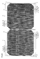
- Fig. 1 is a plan view of a solar cell having wiring sheet according to a first embodiment of the invention when viewed from a light receiving side.
- a solar cell having wiring sheet 100 is formed such that plural back contact solar cells 20 are electrically connected by wiring materials 16 provided on a surface of an insulating base material 11.
- a wiring sheet is formed by providing wiring materials 16 on the surface of insulating base material 11.
- plural cell disposition portions are two-dimensionally arrayed in a row direction and a column direction in order to dispose back contact solar cell 20.
- the electric connection mode of back contact solar cell 20 is not limited to the first embodiment, but a parallel connection and a combination of the series connection and the parallel connection are also included in the electric connection mode of back contact solar cell 20.
- Fig. 2 is a perspective view illustrating a disposition relationship between the back contact solar cell and the wiring sheet. Only part of solar cell having wiring sheet 100 in Fig. 1 is illustrated in Fig. 2 .
- wiring material 16 of wiring sheet 10 constitutes a first wiring for first conductivity type 12 and a second wiring second conductivity type 13.
- First wiring 12 and second wiring 13 are disposed such that comb-tooth portions of comb-shaped first wiring 12 and comb-tooth portions of comb-shaped second wiring 13 are alternately engaged.
- the comb-tooth portions of comb-shaped first wiring 12 and the comb-tooth portions of comb-shaped second wiring 13 are alternately disposed at predetermined intervals.
- Back contact solar cells 20 are placed on wiring sheets 10 to prepare solar cell having wiring sheet 100.
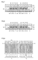
- Fig. 3 is a sectional view taken on a line III-III of Fig. 2 when viewed from an arrow direction.
- An observation device 15 that is not included in solar cell having wiring sheet 100 is also illustrated in Fig. 3 .
- back contact solar cell 20 includes a semiconductor substrate 21, such as a silicon substrate having a conductivity type of an n-type or a p-type, an antireflection film 27 that is formed on an uneven surface of semiconductor substrate 21 constituting a light receiving surface of back contact solar cell 20, and a passivation film 26 that is formed on a back surface of semiconductor substrate 21 constituting a back surface of back contact solar cell 20.
- a semiconductor substrate 21 such as a silicon substrate having a conductivity type of an n-type or a p-type
- an antireflection film 27 that is formed on an uneven surface of semiconductor substrate 21 constituting a light receiving surface of back contact solar cell 20
- a passivation film 26 that is formed on a back surface of semiconductor substrate 21 constituting a back surface of back contact solar cell 20.
- First-conductivity-type impurity diffusion regions 22, each of which is formed by diffusion of a first-conductivity-type impurity, and second-conductivity-type impurity diffusion regions 23, each of which is formed by diffusion of a second-conductivity-type impurity, are alternately formed at predetermined intervals in a back surface of semiconductor substrate 21.
- An electrode for first conductivity type 24, which contacts with first-conductivity-type impurity diffusion region 22 through a contact hole made in passivation film 26 of the back surface of semiconductor substrate 21, and an electrode for second conductivity type 25, which contacts with second-conductivity-type impurity diffusion region 23 through the contact hole, are provided in the back surface of semiconductor substrate 21.
- the conductivity type is the n-type
- phosphorus and the like can be used as the first-conductivity-type diffusion impurity and the second-conductivity-type diffusion impurity.
- the conductivity type is the p-type
- boron and the like can be used.
- Plural pn junctions are formed by the above configuration at an interface between first-conductivity-type impurity diffusion region 22 or second-conductivity-type impurity diffusion region 23 and an inside of semiconductor substrate 21.
- the pn junction may be formed by a contact of first-conductivity-type impurity diffusion region 22 with second-conductivity-type impurity diffusion region 23 that is close to first-conductivity-type impurity diffusion region 22.
- each of electrode for first conductivity type 24 and electrode for second conductivity type 25 constitutes an electrode corresponding to each of the plural pn junctions formed in the back surface of semiconductor substrate 21.
- At least a partial surface of one of or both electrode for first conductivity type 24 and electrode for second conductivity type 25 of back contact solar cell 20 may be coated with an electric conductor containing at least one kind of material selected from a group consisting of nickel (Ni), gold (Au), platinum (Pt), palladium (Pd), silver (Ag), tin (Sn), Sn-Pb solder, and ITO (Indium Tin Oxide).
- This provides good electric connection between wiring material 16 of wiring sheet 10 and the coated electrode of back contact solar cell 20, and a weather resistance of the electrode of back contact solar cell 20 can be improved.
- a surface treatment such as blacking processing, may be performed to at least the partial surface of one of or both electrode for first conductivity type 24 and electrode for second conductivity type 25 of back contact solar cell 20.
- a silicon substrate made of polycrystalline silicon or a single-crystal silicon, which has the conductivity type of the n-type or the p-type, can be used as semiconductor substrate 21.
- the electrode made of metal such as silver
- the electrode made of metal can be used as electrode for first conductivity type 24 and electrode for second conductivity type 25.
- a silicon oxide film, a silicon nitride film, or a laminated body of the silicon oxide film and the silicon nitride film can be used as passivation film 26.
- the silicon nitride film can be used as antireflection film 27.
- a concept of the back contact solar cell of the invention includes not only the above configuration in which both electrode for first conductivity type 24 and electrode for second conductivity type 25 are formed only on the back surface of the semiconductor substrate 21, but also what is called a back contact solar cell, such as an MWT (Metal Wrap Through) cell that is a solar cell having a configuration in which part of the electrode is disposed in a through-hole made in the semiconductor substrate.
- MWT Metal Wrap Through
- electrode first conductivity type 24 of back contact solar cell 20 is electrically connected to first wiring 12 of wiring sheet 10.
- Electrode for second conductivity type 25 of back contact solar cell 20 is electrically connected to second wiring 13 of wiring sheet 10.
- an alignment mark is provided in the back contact solar cell, and a different shape portion is provided in the wiring of the wiring sheet.
- an alignment method as illustrated in Fig. 3 , relative positions of back contact solar cell 20 and wiring sheet 10 are adjusted while the alignment mark is checked from a direction of an arrow A or an arrow B using observation device 15. The alignment mark of the first embodiment will be described below.
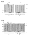
- Fig. 4 is a plan view illustrating the back surface of the back contact solar cell of the first embodiment. Only a column L 1 and a column L 2 in Fig. 1 are partially illustrated in Fig. 4 .
- the alignment mark of back contact solar cell 20 is formed in an inner region located inside of an outer periphery of the electrode pattern including the plural electrodes, which are formed on one of surface sides of semiconductor substrate 21 constituting back contact solar cell 20.
- a boundary line of the inner region is indicated by a dotted line.
- the inner region contains all the electrodes included in the electrode pattern provided with plural electrodes for first conductivity type 24 and plural electrodes for second conductivity type 25 in one back contact solar cell 20, and the inner region is formed by one polygon in which an interior angle is less than or equal to 180 °. Accordingly, in the case that a line continuously connecting end portions of the electrodes is locally dented, part of the boundary line of the inner region is formed by a line connecting both ends of the dented portion.
- electrode for second conductivity type 25 in a column in which an alignment mark 25a or an alignment mark 25b is provided is formed shorter than other electrodes for first conductivity type 24 and other electrodes for second conductivity type 25.
- the inner region is defined by other electrodes for first conductivity type 24 and other electrodes for second conductivity type 25 (the region indicated by the dotted line) irrespective of shortly-formed electrode for second conductivity type 25.
- circular-point-like alignment marks 25a and 25b are formed near a leading end of shortly-formed electrode for second conductivity type 25. That is, alignment marks 25a and 25b are located in a space where the plural electrodes are not located in the inner region.
- the electrode pattern includes plural electrode lines in which plural linearly-extending electrodes for first conductivity type 24 and plural linearly-extending electrodes for second conductivity type 25 are arrayed in parallel.
- the space is formed such that one of end portions in an electrode extending direction in at least one of the plural electrode lines is located inside of one of end portions in each of other electrode lines in the extending direction.
- alignment marks 25a and 25b are formed on an extended line of the electrode line.
- each of alignment marks 25a and 25b may be formed between the electrode lines adjacent to each other.
- alignment marks 25a and 25b are formed in the inner region, so that the alignment between back contact solar cell 20 and wiring sheet 10 can be achieved without enlarging the region where the power is not taken out.
- Back contact solar cell 20 disposed in column L 1 and back contact solar cell 20 disposed in column L2 have the same electrode pattern.
- Alignment mark 25a formed in back contact solar cell 20 disposed in column L 1 and alignment mark 25b formed in back contact solar cell 20 disposed in column L2 are disposed so as to be overlapped with each other when one of back contact solar cells 20 is rotated by 180° in a paper plane of Fig. 4 to overlap patterns of electrodes for first conductivity type 24 with patterns of electrodes for second conductivity type 25. Accordingly, back contact solar cell 20 disposed in column L2 can be disposed by rotating back contact solar cell 20 disposed in column L 1 by 180° in the paper plane.
- Alignment marks 25a and 25b is made of the same material as plural electrodes for first conductivity type 24 and plural electrodes for second conductivity type 25.
- electrode for first conductivity type 24 and electrode for second conductivity type 25 and alignment marks 25a and 25b can be formed in one process.
- accuracy of a positional relationship can be enhanced by preparing electrode for first conductivity type 24 and electrode for second conductivity type 25 and alignment marks 25a and 25b in the same process using photolithography or screen printing.
- widths of alignment marks 25a and 25b is substantially equal to that of the electrode line. Therefore, alignment marks 25a and 25b can be formed without changing an electrode forming process.
- alignment marks 25a and 25b are not limited to the positions in Fig. 4 .
- alignment marks 25a and 25b may be formed in the inner region on the extended line of the electrode line disposed on the outermost side of back contact solar cell 20.
- Fig. 5 is a plan view illustrating the wiring pattern of the wiring sheet of the first embodiment. In Fig. 5 , only the wiring material is illustrated with respect to parts of columns L 1 and L 2 in Fig. 1 .
- wiring sheet 10 includes the wiring in order to electrically connect plural back contact solar cells 20.
- the wiring includes plural identical shape portions having the same shape and at least one different shape portion having a shape different from that of the identical shape portion.
- the wiring includes first wiring 12 that connects electrode for first conductivity type 24 and second wiring 13 that connects electrode for second conductivity type 25.
- First wiring 12 and second wiring 13 are electrically insulated from each other.
- Each of first wiring 12 and second wiring 13 includes plural comb-tooth-shaped portions 17a and a connection wiring portion 17b that connects plural comb-tooth-shaped portions 17a.
- first wiring 12 and second wiring 13 includes the identical shape portion and the different shape portion.
- second wiring 13 includes a different shape portion 13a. Different shape portion 13a such that at least one of plural comb-tooth-shaped portions 17a is shorter than other comb-tooth-shaped portions 17a that are the identical shape portion.
- An alignment target region 18 is defined by different shape portion 13a.
- alignment target region 18 is a wiring non-existence region where wiring material 16 is not disposed on insulating base material 11.
- Alignment target region 18 of wiring sheet 10 disposed in column L 1 and alignment target region 18 of wiring sheet 10 disposed in column L2 are disposed so as to be overlapped with each other when one of wiring sheets 10 is rotated by 180 ° in the paper plane of Fig. 5 to overlap patterns of first wirings 12 with patterns of first wirings 12.
- insulating base material 11 of wiring sheet 10 there is no particular limitation to insulating base material 11 of wiring sheet 10 as long as an electrically insulating material is used.
- a material including at least one kind of resin selected from a group consisting of PET (polyethylene terephthalate), PEN (polyethylene naphthalate) PPS (polyphenylene sulfide), PVF (polyvinyl fluoride), and polyimide.
- Insulating base material 11 There is no particular limitation to a thickness of insulating base material 11.
- the thickness ranges from 10 ⁇ m to 200 ⁇ m.
- Insulating base material 11 may have a single-layer structure or a stacked-layer structure including at least two layers.
- wiring material 16 there is no particular limitation to wiring material 16 as long as an electrically conductive material is used.
- a material including at least one kind of metal selected from a group consisting of copper, aluminum, and silver can be used.
- each of first wiring 12 and second wiring 13 There is no particular limitation to the thickness of each of first wiring 12 and second wiring 13.
- the thickness ranges from 5 ⁇ m to 75 ⁇ m.
- the pattern shape of each of first wiring 12 and second wiring 13 as long as each of first wiring 12 and second wiring 13 has the identical shape portion and the different shape portion, but the pattern shape may properly be set.
- At least a partial surface of one of or both first wiring 12 and second wiring 13 may be coated with an electric conductor containing at least one kind of material selected from a group consisting of nickel (Ni), gold (Au), platinum (Pt), palladium (Pd), silver (Ag), tin (Sn), Sn-Pb solder, and ITO (Indium Tin Oxide).
- an electric conductor containing at least one kind of material selected from a group consisting of nickel (Ni), gold (Au), platinum (Pt), palladium (Pd), silver (Ag), tin (Sn), Sn-Pb solder, and ITO (Indium Tin Oxide).
- First wiring 12 and second wiring 13 may have the single-layer structure or the stacked-layer structure including at least two layers.
- insulating base material 11 such as a PET film
- An electric conductor such as a metallic foil and a metallic plate, is bonded to the whole of one of the surfaces of insulating base material 11.
- alignment target region 18 is set to the wiring non-existence region, preferably a transmittance ratio of insulating base material 11 and wiring material 16 at a specific wavelength becomes ten times or more. Therefore, alignment target region 18 can accurately be recognized in a process of aligning back contact solar cell 20 and wiring sheet 10 with each other.
- Fig. 6 is a plan view illustrating a state in which the back contact solar cell and the wiring sheet of the first embodiment are overlapped with each other when viewed from the back surface side of the solar cell having wiring sheet. Only columns L 1 and L 2 in Fig. 1 are partially illustrated in Fig. 6 .
- back contact solar cell 20 and wiring sheet 10 are aligned with each other such that alignment marks 25a and 25b of back contact solar cell 20 and alignment target regions 18 defined by different shape portions 13a of wiring sheets 10 are disposed while overlapped with each other.
- the wiring non-existence region constituting alignment target region 18 is defined near the leading end of different shape portion 13a, because different shape portion 13a is formed shorter than other first wirings 12 and other second wirings 13, which are the identical shape portion.
- the alignment between back contact solar cell 20 and wiring sheet 10 is performed while back contact solar cell 20 and wiring sheet 10 are observed from the directions of arrows A and B using observation devices 15.
- back contact solar cell 20 and wiring sheet 10 are observed from the direction of arrow A, back contact solar cell 20 is irradiated with light transmitted through back contact solar cell 20 from the side of back contact solar cell 20, and back contact solar cell 20 and wiring sheet 10 are overlapped with each other while alignment marks 25a and 25b and alignment target regions 18 are checked, thereby aligning back contact solar cell 20 and wiring sheet 10 with each other.
- back contact solar cell 20 is irradiated with the light reflected by back contact solar cell 20 from the side of wiring sheet 10, and back contact solar cell 20 and wiring sheet 10 are overlapped with each other while alignment marks 25a and 25b and alignment target regions 18 are checked, thereby aligning back contact solar cell 20 and wiring sheet 10 with each other.
- back contact solar cell 20 and wiring sheet 10 are observed from the direction of arrow B, back contact solar cell 20 is irradiated with the light transmitted through back contact solar cell 20 from the side of wiring sheet 10, and back contact solar cell 20 and wiring sheet 10 are overlapped with each other while alignment marks 25a and 25b and alignment target regions 18 are checked, thereby aligning back contact solar cell 20 and wiring sheet 10 with each other.
- an X-ray and an IR (infrared) ray can be used as the light transmitted through back contact solar cell 20.
- light emitted from an LED (Light Emitting Diode) or a halogen lamp may be used as the light reflected by back contact solar cell 20.
- back contact solar cell 20 and wiring sheet 10 are aligned with each other such that alignment marks 25a and 25b are disposed in alignment target regions 18 and on the extended line of the different shape portion 13a.
- an error in positions of back contact solar cell 20 and wiring sheet 10 can be reduced to 50 ⁇ m or less.
- the solar cell having wiring sheet is formed by joining back contact solar cell 20 and wiring sheet 10.
- the light, with which back contact solar cell 20 is irradiated to observe the alignment mark and the alignment target in the alignment process includes light having a wavelength in which the transmittance ratio of insulating base material 11 and wiring material 16 is greater than or equal to ten times.
- the light includes light having a wavelength in which the transmittance ratio of alignment marks 25a and 25b and surrounding semiconductor substrate 21 is greater than or equal to ten times.
- the light includes light having a wavelength in which the transmittance ratio of alignment marks 25a and 25b and surrounding semiconductor substrate 21 is greater than or equal to five times. Therefore, alignment marks 25a and 25b and alignment target regions 18 can accurately be recognized.
- Fig. 7 is a sectional view illustrating a state before the solar cell having wiring sheet is sealed.
- Fig. 8 is a sectional view illustrating a state in which the solar cell having wiring sheet is sealed to form the solar cell module.
- the solar cell having wiring sheet is disposed between a back-surface protecting sheet 32 and a transparent substrate 33.
- a first transparent resin 31a is disposed between back contact solar cell 20 of the solar cell having wiring sheet and transparent substrate 33.
- a second transparent resin 31 b is disposed between wiring sheet 10 of the solar cell having wiring sheet and back-surface protecting sheet 32.
- first transparent resin 31a and second transparent resin 31b are hardened to constitute a sealing material 31.
- the solar cell module is formed by sealing the solar cell having wiring sheet in sealing material 31.
- Contractive force is generated when first transparent resin 31a and second transparent resin 31b are hardened to constitute sealing material 31.
- the strong pressure bonding of back contact solar cell 20 and wiring sheet 10 is performed by the contractive force.
- the pressing and heating process of sealing the solar cell having wiring sheet in sealing material 31 is performed using a device called a laminator that performs vacuum pressure bonding and the heating process.
- the vacuum pressure bonding is one in which the pressure bonding is performed in a reduced-pressure atmosphere.
- a bubble remaining in sealing material 31 can be suppressed by performing the vacuum pressure bonding.
- a pressure bonding can also be equalized in a joining surface between back contact solar cell 20 and wiring sheet 10.
- transparent substrate 33 there is no particular limitation to transparent substrate 33 as long as a substrate transparent to sunlight is used.
- a glass substrate can be used.
- first transparent resin 31 a and second transparent resin 31 b there is no particular limitation to the materials for first transparent resin 31 a and second transparent resin 31 b as long as a resin transparent to the sunlight is used.
- the same kind of the transparent resin or different kinds of transparent resins may be used as first transparent resin 31 a and second transparent resin 31 b.
- a temperature of the heating process is properly determined according to melting points of first transparent resin 31 a and second transparent resin 31 b.
- An adhesive such as NCP (Non Conductive Paste) and ACP (Anisotropic Conductive Paste) or solder may be used in order to further strengthen the joining between the electrode of back contact solar cell 20 and the wiring of wiring sheet 10.
- the NCP is not applied to the positions of alignment marks 25a and 25b so as not to interrupt the observations of alignment marks 25a and 25b, or the NCP has the high transmittance to the irradiation light used in the alignment process.
- the ACP or the solder preferably the ACP or the solder is applied to at least one of the electrode of back contact solar cell 20 and the wiring of wiring sheet 10.
- back-surface protecting sheet 32 there is no particular limitation to back-surface protecting sheet 32 as long as the back surface of sealing material 31 can be protected.
- a weather-resistance film such as PET, can be used.
- Back-surface protecting sheet 32 may include a metallic film, such as aluminum, in order that permeation of water vapor and oxygen into sealing material 31 is sufficiently suppressed to secure long-term reliability of the solar cell module.
- back-surface protecting sheet 32 and sealing material 31 are brought into close contact with each other using a moisture-permeability preventing tape, such as a butyl rubber tape.
- the solar cell module may be attached so as to be enclosed with a frame made of an aluminum alloy.
- alignment marks 25a and 25b of back contact solar cell 20 are provided on the extended line of electrode for first conductivity type 24, and the different shape portion of wiring sheet 10 may be included in first wiring 12.
- the shapes of alignment marks 25a and 25b are not limited to the circular-point-like shape.
- alignment marks 25a and 25b may have a quadrangular-point-like shape or a triangular-point-like shape.
- alignment marks 25a and 25b are disposed so as not to be overlapped with the wiring.
- alignment marks 25a and 25b may be disposed so as to be partially overlapped with the wiring. In this case, the power is taken out from parts of alignment marks 25a and 25b joined to the wiring, so that the power generation efficiency of the solar cell having wiring sheet can be improved.
- one alignment mark is provided for one back contact solar cell 20.
- plural alignment marks may be provided for one back contact solar cell 20.
- the wiring of wiring sheet 10 includes the different shape portion so as to correspond to the plural alignment marks.
- the good alignment between back contact solar cell 20 and wiring sheet 10 can be performed, and the high-reliability solar cell having wiring sheet and the high-reliability solar cell module can be prepared.
- Back contact solar cell 20 is disposed in a correct position, so that a filling rate of the solar cell having wiring sheet can be enhanced to improve the power generation efficiency per unit area of the solar cell module.
- a back contact solar cell, a wiring sheet, a solar cell having wiring sheet, a solar cell module, and a production method for the solar cell having wiring sheet according to a second embodiment of the invention will be described below.
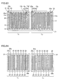
- Fig. 9 is a plan view illustrating a back surface of a back contact solar cell of the second embodiment of the invention. Only columns L 1 and L 2 in Fig. 1 are partially illustrated in Fig. 9 .
- a back contact solar cell 20 of the second embodiment includes an electrode pattern and alignment marks 25a and 25b, which are identical to those of back contact solar cell 20 of the first embodiment.
- Fig. 10 is a plan view illustrating a wiring pattern of a wiring sheet of the second embodiment. In Fig. 10 , only the wiring material is illustrated with respect to parts of columns L 1 and L 2 in Fig. 1 .
- both first wiring 12 and second wiring 13 include the different shape portions. Different shape portion 13a of second wiring 13 is identical to that of the first embodiment.
- a different shape portion 12b of first wiring 12 is formed such that at least one of plural comb-tooth-shaped portions 17a has a shape in which a gap between comb-tooth-shaped portions 17a adjacent to each other is partially widened.
- comb-tooth-shaped portions 17a of first wiring 12, which are formed adjacent to different shape portion 13a of second wiring 13 constitute different shape portions 12b.
- Different shape portion 12b includes a bent portion 18b in which a lateral portion of comb-tooth-shaped portion 17a of first wiring 12 on the side opposite to different shape portion 13a is curved or bent in a position near the leading end of different shape portion 13a. Because different shape portion 12b includes bent portion 18b, comb-tooth-shaped portion 17a of different shape portion 12b is partially thinned compared with other comb-tooth-shaped portions 17a that are the identical shape portions.
- different shape portion 12b is not limited to the above configuration.
- comb-tooth-shaped portion 17a may partially be curved or bent by including bent portion 18b.
- a portion parallel to bent portion 18b is formed in a lateral portion on the opposite side of the lateral portion of comb-tooth-shaped portion 17a, in which bent portion 18b is formed.
- Alignment target regions 18 are defined by different shape portions 12b and different shape portion 13a.
- Alignment target region 18 of wiring sheet 10 disposed in column L 1 and alignment target region 18 of wiring sheet 10 disposed in column L 2 are disposed so as to be overlapped with each other when one of wiring sheets 10 is rotated by 180° in the paper plane of Fig. 10 to overlap the patterns of first wirings 12 with the patterns of second wirings 13.
- the wiring pattern, the electrode pattern corresponding to alignment target region 18, and one kind of back contact solar cell 20 including alignment marks 25a and 25b can commonly be disposed in both columns L 1 and L 2 .
- Fig. 11 is a plan view illustrating a state in which the back contact solar cell and the wiring sheet of the second embodiment are overlapped with each other when viewed from the back surface side of the solar cell having wiring sheet. Only columns L 1 and L 2 in Fig. 1 are partially illustrated in Fig. 11 .
- the alignment between back contact solar cell 20 and wiring sheet 10 is performed such that alignment marks 25a and 25b of back contact solar cell 20 and alignment target region 18 defined by different shape portions 12b and 13a of wiring sheet 10 are disposed while overlapped with each other.
- different shape portion 13a is formed shorter than first wiring 12 and second wiring 13, which are the identical shape portions.
- Different shape portion 12b is partially formed shorter than first wiring 12 and second wiring 13, which are the identical shape portions.
- the wiring non-existence region which constitutes alignment target region 18 while sandwiched between two different shape portions 12b, is defined near the leading end of different shape portion 13a.
- the alignment between back contact solar cell 20 and wiring sheet 10 can be performed with high accuracy such that alignment marks 25a and 25b and alignment target regions 18 are overlapped with each other based on bent portion 18b of different shape portion 12b in addition to the leading end of different shape portion 13a.
- the width of alignment target region 18 is partially increased by bent portion 18b of different shape portion 12b, so that the widths of alignment marks 25a and 25b can be increased according to the increased width of alignment target region 18. In this case, visibility of alignment marks 25a and 25b can be improved.
- one alignment mark is provided for one back contact solar cell 20.
- plural alignment marks may be provided for one back contact solar cell 20.
- the wiring of wiring sheet 10 includes the different shape portion so as to correspond to the plural alignment marks.
- the good alignment between back contact solar cell 20 and wiring sheet 10 can be performed to prepare the high-reliability solar cell having wiring sheet and the high-reliability solar cell module.
- alignment target region 18 can be defined by the comb-tooth-shaped portion in which the different shape portion, such as the bent portion, is formed like the second embodiment.
- a back contact solar cell, a wiring sheet, a solar cell having wiring sheet, a solar cell module, and a production method for the solar cell having wiring sheet according to a third embodiment of the invention will be described below.
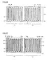
- Fig. 12 is a plan view illustrating a back surface of a back contact solar cell of the third embodiment of the invention. Only columns L 1 and L 2 in Fig. 1 are partially illustrated in Fig. 12 .
- back contact solar cell 20 of the third embodiment of the invention back contact solar cell 20 disposed in column L 1 and back contact solar cell 20 disposed in column L 2 have the identical electrode pattern.
- electrode for second conductivity type 25 is formed short.
- Circular-point-like alignment mark 25a is formed near the leading end of shortly-formed electrode for second conductivity type 25.
- Fig. 13 is a plan view illustrating a wiring pattern of a wiring sheet of the third embodiment. In Fig. 13 , only the wiring material is illustrated with respect to parts of columns L 1 and L 2 in Fig. 1 .
- alignment target region 18 is defined by two different shape portions 12b and different shape portion 13a like wiring sheet 10 of the second embodiment.
- second wiring 13 includes a different shape portion 13c. Different shape portion 13c is formed such that second wiring 13 includes a rectangular opening 18c.
- opening 18c is formed in comb-tooth-shaped portion 17a of second wiring 13, which is located in the center of the direction in which plural comb-tooth-shaped portions 17a are arrayed.
- Alignment target region 18 is defined by different shape portion 13c.
- Opening 18c is not limited to the rectangular shape, but opening 18c may be formed into a circular or polygonal shape. Opening 18c may have the shape, in which alignment mark 25a cab be observed while the surroundings of opening 18c are overlapped with the electrode pattern to cause different shape portion 13c to act as the wiring. Accordingly, opening 18c is not limited to the case that opening 18c is formed in the center of the width direction of the wiring as illustrated in Fig. 13 , but opening 18c may be formed while biased toward the end portion in the width direction of the wiring. It is not always necessary that the whole periphery of opening 18c be surrounded by the wiring, namely, opening 18c may partially be opened.
- Opening 18c may be formed in connection wiring portion 17b, or may be disposed while straddling comb-tooth-shaped portion 17a and connection wiring portion 17b.
- Fig. 14 is a plan view illustrating a state in which the back contact solar cell and the wiring sheet of the third embodiment are overlapped with each other when viewed from the back surface side of the solar cell having wiring sheet. Only columns L 1 and L 2 in Fig. 1 are partially illustrated in Fig. 14 .
- the alignment between back contact solar cell 20 and wiring sheet 10 is performed such that alignment mark 25a of back contact solar cell 20 disposed in column L 1 and alignment target region 18 defined by different shape portions 12b and 13a of wiring sheet 10 are disposed while overlapped with each other.
- the alignment between back contact solar cell 20 and wiring sheet 10 is also performed such that alignment mark 25a of back contact solar cell 20 disposed in column L 2 and alignment target region 18 defined by different shape portion 13c of wiring sheet 10 are disposed while overlapped with each other.
- different shape portion 13c is formed such that the wiring includes opening 18c. Therefore, in different shape portion 13c, comb-tooth-shaped portion 17a and connection wiring portion 17b can be connected through the surrounding of opening 18c. As a result, alignment target region 18 can be formed while the degradation of the power generation efficiency of the solar cell having wiring sheet is suppressed.
- Fig. 15 is a perspective view illustrating the state in which the back contact solar cell and the wiring sheet of the third embodiment are overlapped with each other.
- arrows oriented toward the side on which alignment mark 25a is disposed is illustrated in Fig. 15 .
- back contact solar cell 20 of the third embodiment as described above, back contact solar cell 20 disposed in column L 1 and back contact solar cell 20 disposed in column L 2 have the identical electrode pattern.
- Back contact solar cells 20 are disposed in columns L 1 and L 2 adjacent to each other while back contact solar cell 20 disposed in one of columns L 1 and L 2 is not rotated by 180° in the paper plane. Accordingly, when back contact solar cell 20 is disposed in wiring sheet 10, the orientations of back contact solar cells 20 disposed in columns L 1 and L 2 adjacent to each other can be kept in one direction.
- all back contact solar cells 20 can be disposed on wiring sheet 10 while alignment mark 25a is located on the leading end side indicated by the arrow. Accordingly, component management is easy to perform, and the production process is reduced to improve the production efficiency.
- one alignment mark is provided for one back contact solar cell 20.
- plural alignment marks may be provided for one back contact solar cell 20.
- the wiring of wiring sheet 10 includes the different shape portion so as to correspond to the plural alignment marks.
- the good alignment between back contact solar cell 20 and wiring sheet 10 can be performed to prepare the high-reliability solar cell having wiring sheet and the high-reliability solar cell module.
- a back contact solar cell, a wiring sheet, a solar cell having wiring sheet, a solar cell module, and a production method for the solar cell having wiring sheet according to a fourth embodiment of the invention will be described below.
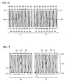
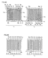
- Fig. 16 is a plan view illustrating a back surface of a back contact solar cell of the fourth embodiment of the invention. Only columns L 1 and L 2 in Fig. 1 are partially illustrated in Fig. 16 .
- back contact solar cell 20 of the fourth embodiment of the invention back contact solar cell 20 disposed in column L 1 and back contact solar cell 20 disposed in column L 2 have the identical electrode pattern.
- an alignment mark 25c is formed in a space of the gap between the electrodes such that at least one of the plural electrode lines is separated in the electrode extending direction.
- electrode for second conductivity type 25 located in the center of the direction in which the electrodes are arrayed is separated in the extending direction of electrode for second conductivity type 25.
- Circular-point-like alignment mark 25c is formed in the gap between the separated electrodes for second conductivity type 25.
- Alignment mark 25c is formed in the substantial center of the back surface of back contact solar cell 20.
- Fig. 17 is a plan view illustrating a wiring pattern of a wiring sheet of the fourth embodiment. In Fig. 17 , only the wiring material is illustrated with respect to parts of columns L 1 and L 2 in Fig. 1 .
- second wiring 13 includes different shape portion 13c. Different shape portion 13c is formed such that second wiring 13 includes rectangular opening 18c.
- opening 18c is formed in comb-tooth-shaped portion 17a of second wiring 13, which is located in the center of the direction in which plural comb-tooth-shaped portions 17a are arrayed. Opening 18c is formed in the center of comb-tooth-shaped portion 17a in the extending direction of comb-tooth-shaped portion 17a. Alignment target region 18 is defined by different shape portion 13c.
- Fig. 18 is a plan view illustrating a state in which the back contact solar cell and the wiring sheet of the fourth embodiment are overlapped with each other when viewed from the back surface side of the solar cell having wiring sheet. Only column L 1 and column L 2 in Fig. 1 are partially illustrated in Fig. 18 .
- the alignment between back contact solar cell 20 and wiring sheet 10 is performed such that alignment mark 25c of back contact solar cell 20 and alignment target region 18 defined by different shape portion 13c of wiring sheet 10 are disposed while overlapped with each other.
- back contact solar cell 20 of the fourth embodiment as described above, back contact solar cell 20 disposed in column L 1 and back contact solar cell 20 disposed in column L 2 have the identical electrode pattern. Alignment mark 25c is located in the center of the back surface of back contact solar cell 20.
- all back contact solar cells 20 can be disposed on wiring sheet 10 while alignment mark 25a is located on the leading end side indicated by the arrow. Accordingly, the component management is easy to perform, and the process to rotate back contact solar cell 20 is reduced to improve the production efficiency.
- one alignment mark is provided for one back contact solar cell 20.
- plural alignment marks may be provided for one back contact solar cell 20.
- the wiring of wiring sheet 10 includes the different shape portion so as to correspond to the plural alignment marks.
- the good alignment between back contact solar cell 20 and wiring sheet 10 can be performed to prepare the high-reliability solar cell having wiring sheet and the high-reliability solar cell module.
- a back contact solar cell, a wiring sheet, a solar cell having wiring sheet, a solar cell module, and a production method for the solar cell having wiring sheet according to a fifth embodiment of the invention will be described below.
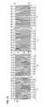
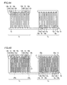
- Fig. 19 is a plan view illustrating a back surface of a back contact solar cell of the fifth embodiment of the invention. Only column L 1 , column L 1 column L 2 , and column L 2' in Fig. 1 are partially illustrated in Fig. 19 .
- back contact solar cell 20 of the fifth embodiment of the invention back contact solar cell 20 disposed in column L 1 . and back contact solar cell 20 disposed in column L 2 have the identical electrode pattern.
- Back contact solar cell 20 disposed in column L 1 and back contact solar cell 20 disposed in column L 2' have the identical electrode pattern.
- each of alignment marks 28 and 29 is formed between the electrode lines adjacent to each other in the plural electrode lines.
- alignment mark 28 is formed between electrode for first conductivity type 24, which is disposed second from the left, and electrode for second conductivity type 25, which is disposed third from the left. Alignment mark 28 is formed in the inner region. Alignment mark 28 is formed near one of the end portions of the electrode in the electrode extending direction.
- alignment mark 29 is formed between electrode for first conductivity type 24, which is disposed second from the right, and electrode for second conductivity type 25, which is disposed third from the left. Alignment mark 29 is formed in the inner region. Alignment mark 29 is formed near the other end portion of the electrode in the electrode extending direction.
- Alignment marks 29 formed in back contact solar cells 20 disposed in columns L 1 and L 2 , and alignment marks 28 formed in back contact solar cell 20 disposed in columns L 1' and L 2 are disposed so as to be overlapped with each other when one of back contact solar cells 20 is rotated by 180° in the paper plane of Fig. 19 to overlap patterns of electrodes for first conductivity type 24 with patterns of electrodes for second conductivity type 25. Accordingly, back contact solar cells 20 disposed in columns L 1 and L 2' can be disposed such that back contact solar cells 20 disposed in columns L 1' and L 2 are rotated by 180° in the paper plane.
- Fig. 20 is a plan view illustrating a wiring pattern of a wiring sheet of the fifth embodiment. In Fig. 20 , only the wiring material is illustrated with respect to parts of column L 1 , column L 1' , column L 2 , and column L 2' in Fig. 1 .
- both first wiring 12 and second wiring 13 include the different shape portion.
- the different shape portion is formed such that the gap between at least one set of comb-tooth-shaped portions 17a adjacent to each other is partially increased.
- comb-tooth-shaped portion 17a of first wiring 12 which is formed second from the right, constitutes a different shape portion 12d.
- comb-tooth-shaped portion 17a of first wiring 12 which is formed second from the left, constitutes different shape portion 12d.
- Comb-tooth-shaped portion 17a of first wiring 12, which is formed third from the left, constitutes different shape portion 13d.
- Different shape portion 12d and different shape portion 13d are formed opposite each other.
- Each of different shape portion 12d and different shape portion 13d includes a bent portion 18d in which the lateral portion of comb-tooth-shaped portion 17a on the side on which different shape portion 12d and different shape portion 13d are formed opposite each other is curved or bent, and each of different shape portion 12d and different shape portion 13d is formed such that comb-tooth-shaped portion 17a is partially thinned compared with other comb-tooth-shaped portions 17a that are the identical shape portion.
- different shape portion 12d and different shape portion 13d are not limited to the above configuration.
- different shape portion 12d and different shape portion 13d may partially be curved and bent by including bent portion 18d.
- a portion parallel to bent portion 18d is formed in a lateral portion on the opposite side of the lateral portion of comb-tooth-shaped portion 17a, in which bent portion 18d is formed.
- Alignment target region 18 is defined by different shape portions 12d and different shape portion 13d.
- Alignment target regions 18 of wiring sheets 10 disposed in columns L 1 and L 2' and alignment target regions 18 of wiring sheets 10 disposed in columns L 1 and L 2 are disposed so as to be overlapped with each other when one of wiring sheets 10 is rotated by 180° in the paper plane of Fig. 20 to overlap the patterns of first wirings 12 with the patterns of second wiring 13.
- the wiring pattern, the electrode pattern corresponding to alignment target region 18, and one kind of back contact solar cell 20 including alignment marks 25a and 25b can commonly be disposed in all column L 1 , column L 1' , column L 2 , and column L 2' .
- Fig. 21 is a plan view illustrating a state in which the back contact solar cell and the wiring sheet of the fifth embodiment are overlapped with each other when viewed from the back surface side of the solar cell having wiring sheet. Only column L 1 , column L 1 ', column L 2 , and column L 2' in Fig. 1 are partially illustrated in Fig. 21 .
- the alignment between back contact solar cell 20 and wiring sheet 10 is performed such that alignment marks 28 and 29 of back contact solar cells 20 and alignment target regions 18 defined by different shape portions 12d and 13d of wiring sheet 10 are disposed while overlapped with each other.
- different shape portion 12d and different shape portion 13d are partially thinned compared with other first wirings 12 and other second wirings 13, which are the identical shape portion, thereby defining the wiring non-existence region that constitutes alignment target region 18 sandwiched between different shape portion 12d and different shape portion 13d.
- the alignment between back contact solar cell 20 and wiring sheet 10 can be performed with high accuracy such that alignment marks 28 and 29 and alignment target regions 18 are overlapped with each other based on bent portions 18d of different shape portion 12d and different shape portion 13d.
- the fifth embodiment unlike back contact solar cell 20 of the first embodiment, it is not necessary to partially shorten the electrode line in order to define alignment target region 18. Therefore, the power generation efficiency of the solar cell having wiring sheet can be improved.
- two alignment marks are provided for one back contact solar cell 20.
- plural alignment marks may be provided for one back contact solar cell 20.
- the wiring of wiring sheet 10 includes the different shape portion so as to correspond to the plural alignment marks.
- the good alignment between back contact solar cell 20 and wiring sheet 10 can be performed to prepare the high-reliability solar cell having wiring sheet and the high-reliability solar cell module.
- a back contact solar cell, a wiring sheet, a solar cell having wiring sheet, a solar cell module, and a production method for the solar cell having wiring sheet according to a sixth embodiment of the invention will be described below.
- Fig. 22 is a plan view illustrating a back surface of a back contact solar cell of the sixth embodiment of the invention. Only columns L 1 and L 2 in Fig. 1 are partially illustrated in Fig. 22 .
- electrodes for second conductivity type 25 which are disposed third from the left and third from the right in the direction in which the electrodes are arrayed, are formed shorter than other electrodes for first conductivity type 24 and other electrodes for second conductivity type 25.
- Circular-point-like alignment mark 25a is formed near the leading end of shortly-formed electrode for second conductivity type 25. That is, alignment mark 25a is located in the space where the electrode is not located in the inner region.
- plural alignment marks 25a are formed near one of the end portions of the electrode in the electrode extending direction.
- plural alignment marks 25b are formed near the other end portion of the electrode in the electrode extending direction.
- Alignment mark 25a formed in back contact solar cell 20 disposed in column L 1 and alignment mark 25b formed in back contact solar cell 20 disposed in column L 2 are disposed so as to be overlapped with each other when one of back contact solar cells 20 is rotated by 180° in the paper plane of Fig. 22 to overlap the patterns of electrodes for first conductivity type 24 with the patterns of electrodes for second conductivity type 25. Accordingly, back contact solar cell 20 disposed in column L 2 can be disposed such that back contact solar cell 20 disposed in column L 1 is rotated by 180° in the paper plane.
- Fig. 23 is a plan view illustrating a wiring pattern of a wiring sheet of the sixth embodiment. In Fig. 23 , only the wiring material is illustrated with respect to parts of columns L 1 and L 2 in Fig. 1 .
- second wiring 13 includes different shape portions 13a. Different shape portions 13a are formed such that plural comb-tooth-shaped portions 17a are formed shorter than other comb-tooth-shaped portions 17a that are the identical shape portion.
- comb-tooth-shaped portions 17a of second wiring 13, which are disposed third from the left and third from the right in the direction in which plural comb-tooth-shaped portions 17a are arrayed, are formed shorter than other comb-tooth-shaped portions 17a.
- Alignment target region 18 is defined by different shape portion 13a.
- Alignment target region 18 of wiring sheet 10 disposed in column L 1 and alignment target region 18 of wiring sheet 10 disposed in column L 2 are disposed so as to be overlapped with each other when one of wiring sheets 10 is rotated by 180° in the paper plane of Fig. 23 to overlap the patterns of first wirings 12 with the patterns of second wirings 13.
- Fig. 24 is a plan view illustrating a state in which the back contact solar cell and the wiring sheet of the sixth embodiment are overlapped with each other when viewed from the back surface side of the solar cell having wiring sheet. Only columns L 1 and L 2 in Fig. 1 are partially illustrated in Fig. 24 .
- the alignment between back contact solar cell 20 and wiring sheet 10 is performed such that alignment marks 25a and 25b of back contact solar cell 20 and alignment target regions 18 defined by different shape portions 13a of wiring sheet 10 are disposed while overlapped with each other.
- the alignment between back contact solar cell 20 and wiring sheet 10 can accurately be performed in not only the vertical and horizontal directions also the rotating direction.
- the good alignment between back contact solar cell 20 and wiring sheet 10 can be performed to prepare the high-reliability solar cell having wiring sheet and the high-reliability solar cell module.
- a back contact solar cell, a wiring sheet, a solar cell having wiring sheet, a solar cell module, and a production method for the solar cell having wiring sheet according to a seventh embodiment of the invention will be described below.
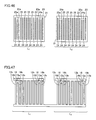
- Fig. 25 is a plan view illustrating a back surface of a back contact solar cell of the seventh embodiment of the invention. Only columns L 1 and L 2 in Fig. 1 are partially illustrated in Fig. 25 .
- back contact solar cell 20 of the seventh embodiment of the invention back contact solar cell 20 disposed in column L 1 and back contact solar cell 20 disposed in column L 2 have the identical electrode pattern.
- Electrode for first conductivity type 24, which is disposed second from the right, and electrode for second conductivity type 25, which is disposed third from the left, are formed short.
- Circular-point-like alignment mark 24a is formed near the leading end of shortly-formed electrode for first conductivity type 24.
- Circular-point-like alignment mark 25a is formed near the leading end of shortly-formed electrode for second conductivity type 25.
- two alignment marks 24a and 25a are formed on the extended lines of the electrode lines having different conductivity types, respectively.
- Fig. 26 is a plan view illustrating a wiring pattern of a wiring sheet of the seventh embodiment. In Fig. 26 , only the wiring material is illustrated with respect to parts of columns L 1 and L 2 in Fig. 1 .
- first wiring 12 and second wiring 13 include different shape portion 12a and different shape portion 13a, respectively.
- Different shape portions 12a and 13a are formed such that at least one of plural comb-tooth-shaped portions 17a is formed shorter than other comb-tooth-shaped portions 17a that are the identical shape portion.
- comb-tooth-shaped portion 17a of second wiring 13 which is disposed third from the left in the direction in which plural comb-tooth-shaped portions 17a are arrayed, is formed shorter than other comb-tooth-shaped portions 17a.
- comb-tooth-shaped portion 17a of first wiring 12 which is disposed second from the right in the direction in which plural comb-tooth-shaped portions 17a are arrayed, is formed shorter than other comb-tooth-shaped portions 17a.
- alignment target region 18 is defined by different shape portion 13a.
- alignment target region 18 is defined by different shape portion 12a.
- Fig. 27 is a plan view illustrating a state in which the back contact solar cell and the wiring sheet of the seventh embodiment are overlapped with each other when viewed from the back surface side of the solar cell having wiring sheet. Only columns L 1 and L 2 in Fig. 1 are partially illustrated in Fig. 27 .
- alignment mark 25a of back contact solar cell 20 and alignment target region 18 defined by different shape portion 13a of wiring sheet 10 are disposed as to be overlapped with each other.
- Comb-tooth-shaped portion 17a of first wiring 12 and alignment mark 24a are disposed so as to be overlapped with each other.
- alignment mark 24a of back contact solar cell 20 and alignment target region 18 defined by different shape portion 12a of wiring sheet 10 are disposed so as to be overlapped with each other.
- Comb-tooth-shaped portion 17a of second wiring 13 and alignment mark 25a are disposed so as to be overlapped with each other.
- back contact solar cell 20 including plural alignment marks, at least one alignment mark is disposed so as to be overlapped with alignment target region 18, and at least one alignment mark is disposed so as to be overlapped with the wiring, thereby performing the alignment between back contact solar cell 20 and wiring sheet 10.
- the alignment between back contact solar cell 20 and wiring sheet 10 can accurately be performed using two alignment marks 24a and 25a.
- alignment mark 24a and alignment mark 25a can be distinguished from each other by forming alignment mark 24a and alignment mark 25a into different shapes, the alignment between back contact solar cell 20 disposed in column L 1 and back contact solar cell 20 disposed in column L 2 can accurately be performed while alignment marks 24a and 25a are distinguished from each other.
- the alignment between back contact solar cell 20 and wiring sheet 10 may be performed such that at least one alignment mark is disposed so as to be overlapped with alignment target region 18, or such that at least one alignment mark is disposed so as to be overlapped with the wiring.
- back contact solar cell 20 of the seventh embodiment back contact solar cell 20 disposed in column L 1 and back contact solar cell 20 disposed in column L 2 have the identical electrode pattern.
- Back contact solar cells 20 are disposed in columns L 1 and L 2 adjacent to each other while back contact solar cell 20 disposed in one of columns L 1 and L 2 is not rotated by 180° in the paper plane. Accordingly, when back contact solar cell 20 is disposed in wiring sheet 10, the orientations of back contact solar cells 20 disposed in columns L 1 and L 2 adjacent to each other can be kept in one direction.
- all back contact solar cells 20 can be disposed on wiring sheet 10 while alignment marks 24a and 25a are located on the leading end side indicated by the arrow. Accordingly, the component management is easy to perform, and the production process is reduced to improve the production efficiency.
- alignment mark 24a and alignment mark 25a can be distinguished from each other, for example, when alignment mark 24a and alignment mark 25a are located on the extended line of the electrode lines having the different conductivity types, it can be checked that the alignment between back contact solar cell 20 and wiring sheet 10 is performed such that electrode for first conductivity type 24 of back contact solar cell 20 is properly connected to first wiring 12 of the corresponding wiring sheet, and it can be checked that the alignment between back contact solar cell 20 and wiring sheet 10 is performed such that electrode for second conductivity type 25 of back contact solar cell 20 is properly connected to second wiring 13 of the corresponding wiring sheet. Therefore, production of a defective product, which is caused by an unintended misalignment, can securely be prevented.
- each two of the alignment marks and the different shape portions are provided for one solar cell having wiring sheet.
- the numbers of alignment marks and different shape portions are not limited to those of the seventh embodiment.
- the good alignment between back contact solar cell 20 and wiring sheet 10 can be performed to prepare the high-reliability solar cell having wiring sheet and the high-reliability solar cell module.
- a back contact solar cell, a wiring sheet, a solar cell having wiring sheet, a solar cell module, and a production method for the solar cell having wiring sheet according to an eighth embodiment of the invention will be described below.
- Fig. 28 is a plan view illustrating a back surface of a back contact solar cell of the eighth embodiment of the invention.
- back contact solar cell 20 of the eighth embodiment of the invention back contact solar cell 20 disposed in column L 1 and back contact solar cell 20 disposed in column L 2 have the identical electrode pattern.
- Back contact solar cell 20 of the eighth embodiment has the same electrode pattern as back contact solar cell 20 of the seventh embodiment.
- Fig. 29 is a plan view illustrating a wiring pattern of a wiring sheet of the eighth embodiment. In Fig. 29 , only the wiring material is illustrated with respect to parts of columns L 1 and L 2 in Fig. 1 .
- first wiring 12 includes different shape portions 12a and 12c.
- Second wiring 13 includes different shape portions 13a and 13c. Different shape portion 12a and 13a are formed such that at least one of plural comb-tooth-shaped portions 17a is shorter than other comb-tooth-shaped portions 17a that are the identical shape portion.
- comb-tooth-shaped portion 17a of second wiring 13 which is disposed third from the left in the direction in which plural comb-tooth-shaped portions 17a are arrayed, is formed shorter than other comb-tooth-shaped portions 17a.
- comb-tooth-shaped portion 17a of first wiring 12 which is disposed second from the right in the direction in which plural comb-tooth-shaped portions 17a are arrayed, is formed shorter than other comb-tooth-shaped portions 17a.
- first wiring 12 and second wiring 13 include rectangular openings 18c.
- opening 18c is formed in comb-tooth-shaped portion 17a of first wiring 12, which is disposed second from the right.
- opening 18c is formed in comb-tooth-shaped portion 17a of second wiring 13, which is disposed third from the left.
- opening 18c may be formed in connection wiring portion 17b, or may be formed while straddling comb-tooth-shaped portion 17a and connection wiring portion 17b.
- alignment target regions 18 are defined by different shape portion 12c and different shape portion 13a, respectively.
- alignment target regions 18 are defined by different shape portion 12a and different shape portion 13c, respectively.
- Fig. 30 is a plan view illustrating a state in which the back contact solar cell and the wiring sheet of the eighth embodiment are overlapped with each other when viewed from the back surface side of the solar cell having wiring sheet. Only columns L 1 and L 2
- alignment mark 25a of back contact solar cell 20 and alignment target region 18 defined by different shape portion 13a of wiring sheet 10 are disposed while overlapped with each other.
- Alignment mark 24a of back contact solar cell 20 and alignment target region 18 defined by different shape portion 12c of wiring sheet 10 are disposed while overlapped with each other.
- alignment mark 24a of back contact solar cell 20 and alignment target region 18 defined by different shape portion 12a of wiring sheet 10 are disposed while overlapped with each other.
- Alignment mark 25a of back contact solar cell 20 and alignment target region 18 defined by different shape portion 13c of wiring sheet 10 are disposed while overlapped with each other.
- back contact solar cell 20 including plural alignment marks
- at least two alignment marks are disposed so as to be overlapped with alignment target regions 18, thereby performing the alignment between back contact solar cell 20 and wiring sheet 10.
- the alignment between back contact solar cell 20 and wiring sheet 10 can accurately be performed in not only the vertical and horizontal directions also the rotating direction.
- alignment mark 24a and alignment mark 25a can be distinguished from each other in each back contact solar cell 20, for example, when alignment mark 24a and alignment mark 25a are located on the extended line of the electrode lines having the different conductivity types, it can be checked that the alignment between back contact solar cell 20 and wiring sheet 10 is performed such that electrode for first conductivity type 24 of back contact solar cell 20 is properly connected to first wiring 12 of the corresponding wiring sheet, and it can be checked that the alignment between back contact solar cell 20 and wiring sheet 10 is performed such that electrode for second conductivity type 25 of back contact solar cell 20 is properly connected to second wiring 13 of the corresponding wiring sheet. Therefore, the production of the defective product, which is caused by an unintended misalignment, can securely be prevented.
- each two of the alignment marks and the different shape portions are provided for one solar cell having wiring sheet.
- the numbers of alignment marks and different shape portions are not limited to those of the eighth embodiment.
- the good alignment between back contact solar cell 20 and wiring sheet 10 can be performed to prepare the high-reliability solar cell having wiring sheet and the high-reliability solar cell module.
- a back contact solar cell, a wiring sheet, a solar cell having wiring sheet, a solar cell module, and a production method for the solar cell having wiring sheet according to a ninth embodiment of the invention will be described below.
- Fig. 31 is a plan view illustrating a back surface of a back contact solar cell of the ninth embodiment of the invention. Only columns L 1 and L 2 in Fig. 1 are partially illustrated in Fig. 31 .
- back contact solar cell 20 of the ninth embodiment of the invention back contact solar cell 20 disposed in column L 1 and back contact solar cell 20 disposed in column L 2 have the identical electrode pattern.
- electrodes for second conductivity type 25 which are disposed third from the left and third from the right in the direction in which the electrodes are arrayed, are formed shorter than other electrodes for first conductivity type 24 and other electrodes for second conductivity type 25.
- Circular-point-like alignment marks 25a and 25b are formed near the leading ends of the shortly-formed electrodes for second conductivity type 25.
- Alignment mark 25a is formed near one of the end portions of the electrode in the electrode extending direction, and alignment mark 25b is formed near the other end portion of the electrode.
- Fig. 32 is a plan view illustrating a wiring pattern of a wiring sheet of the ninth embodiment. In Fig. 32 , only the wiring material is illustrated with respect to parts of columns L 1 and L 2 in Fig. 1 .
- second wiring 13 includes different shape portion 13a.
- Different shape portion 13a is formed such that plural comb-tooth-shaped portions 17a are shorter than other comb-tooth-shaped portions 17a.
- comb-tooth-shaped portion 17a of second wiring 13 which is disposed third from the left in the direction in which plural comb-tooth-shaped portions 17a are arrayed, is formed shorter than other comb-tooth-shaped portions 17a.
- comb-tooth-shaped portion 17a of second wiring 13 which is disposed third from the right in the direction in which plural comb-tooth-shaped portions 17a are arrayed, is formed shorter than other comb-tooth-shaped portions 17a.
- Alignment target region 18 is defined by different shape portion 13a.
- Alignment target region 18 of wiring sheet 10 disposed in column L 1 and alignment target region 18 of wiring sheet 10 disposed in column L 2 are disposed so as to be overlapped with each other when one of wiring sheets 10 is rotated by 180° in the paper plane of Fig. 32 to overlap the patterns of first wirings 12 with the patterns of second wirings 13.
- Fig. 33 is a plan view illustrating a state in which the back contact solar cell and the wiring sheet of the ninth embodiment are overlapped with each other when viewed from the back surface side of the solar cell having wiring sheet. Only columns L 1 and L 2 in Fig. 1 are partially illustrated in Fig. 33 .
- alignment mark 25a of back contact solar cell 20 and alignment target region 18 defined by different shape portion 13a of wiring sheet 10 are disposed while overlapped with each other.
- Comb-tooth-shaped portion 17a of second wiring 13 and alignment mark 25b are disposed so as to be overlapped with each other.
- alignment mark 25b of back contact solar cell 20 and alignment target region 18 defined by different shape portion 13a of wiring sheet 10 are disposed while overlapped with each other.
- Comb-tooth-shaped portion 17a of second wiring 13 and alignment mark 25a are disposed so as to be overlapped with each other.
- back contact solar cell 20 including plural alignment marks, at least one alignment mark is disposed so as to be overlapped with alignment target regions 18, and at least one alignment mark is disposed so as to be overlapped with the wiring, thereby performing the alignment between back contact solar cell 20 and wiring sheet 10.
- the alignment between back contact solar cell 20 and wiring sheet 10 may be performed such that at least one alignment mark is disposed so as to be overlapped with alignment target region 18, or such that at least one alignment mark is disposed so as to be overlapped with the wiring.
- each two of the alignment marks and the different shape portions are provided for one solar cell having wiring sheet.
- the numbers of alignment marks and different shape portions are not limited to those of the ninth embodiment.
- back contact solar cell 20 disposed in column L 1 and back contact solar cell 20 disposed in column L 2 have the identical electrode pattern.
- Back contact solar cells 20 are disposed in columns L 1 and L 2 adjacent to each other while back contact solar cell 20 disposed in one of columns L 1 and L 2 is not rotated by 180° in the paper plane. Accordingly, when back contact solar cell 20 is disposed in wiring sheet 10, the orientations of back contact solar cells 20 disposed in columns L 1 and L 2 adjacent to each other can be kept in one direction.
- all back contact solar cells 20 can be disposed on wiring sheet 10 while kept in one direction. Accordingly, the component management is easy to perform, and the process to rotate back contact solar cell 20 is reduced to improve the production efficiency.
- Alignment mark 25a and alignment mark 25b are symmetrically formed with respect to the center of the back surface of back contact solar cell 20. Therefore, the alignment between back contact solar cell 20 and wiring sheet 10 can be performed even if back contact solar cell 20 is rotated by 180° in the paper plane. Accordingly, the management in the direction of back contact solar cell 20 can be simplified to improve the production efficiency.
- the good alignment between back contact solar cell 20 and wiring sheet 10 can be performed to prepare the high-reliability solar cell having wiring sheet and the high-reliability solar cell module.
- a back contact solar cell, a wiring sheet, a solar cell having wiring sheet, a solar cell module, and a production method for the solar cell having wiring sheet according to a tenth embodiment of the invention will be described below.
- Fig. 34 is a plan view illustrating a back surface of a back contact solar cell of the tenth embodiment of the invention. Only columns L 1 and L 2 in Fig. 1 are partially illustrated in Fig. 34 .
- back contact solar cell 20 of the tenth embodiment of the invention back contact solar cell 20 disposed in column L 1 and back contact solar cell 20 disposed in column L 2 have the identical electrode pattern.
- Back contact solar cell 20 of the tenth embodiment has the same electrode pattern as the back contact solar cell 20 of the ninth embodiment.
- Fig. 35 is a plan view illustrating a wiring pattern of a wiring sheet of the tenth embodiment. In Fig. 35 , only the wiring material is illustrated with respect to parts of columns L 1 and L 2 in Fig. 1 .
- second wiring 13 includes different shape portion 13a and 13c.
- Different shape portion 13a is formed such that at least one of plural comb-tooth-shaped portions 17a is shorter than other comb-tooth-shaped portions 17a that are the identical shape portion.
- comb-tooth-shaped portion 17a of second wiring 13 which is disposed third from the right in the direction in which plural comb-tooth-shaped portions 17a are arrayed, is formed shorter than other comb-tooth-shaped portions 17a.
- comb-tooth-shaped portion 17a of second wiring 13 which is disposed third from the right in the direction in which plural comb-tooth-shaped portions 17a are arrayed, is formed shorter than other comb-tooth-shaped portions 17a.
- Different shape portion 13c is formed such that second wiring 13 has rectangular opening 18c.
- opening 18c is formed in comb-tooth-shaped portion 17a.
- Comb-tooth-shaped portion 17a of second wiring 13, which is disposed third from the right, is formed in wiring sheet 10 disposed in column L 1 .
- In wiring sheet 10 disposed in column L 2 Comb-tooth-shaped portion 17a of second wiring 13, which is disposed third from the left, is formed in wiring sheet 10 disposed in column L 2 .
- opening 18c may be formed in connection wiring portion 17b, or may be formed while straddling comb-tooth-shaped portion 17a and connection wiring portion 17b.
- alignment target regions 18 are defined by different shape portion 13a and different shape portion 13c, respectively.
- Fig. 36 is a plan view illustrating a state in which the back contact solar cell and the wiring sheet of the tenth embodiment are overlapped with each other when viewed from a back surface side of the solar cell having wiring sheet. Only columns L 1 and L 2 in Fig. 1 are partially illustrated in Fig. 36 .
- alignment mark 25a of back contact solar cell 20 and alignment target region 18 defined by different shape portion 13a of wiring sheet 10 are disposed while overlapped with each other.
- Alignment mark 25b of back contact solar cell 20 and alignment target region 18 defined by different shape portion 13c of wiring sheet 10 are disposed while overlapped with each other.
- alignment mark 25b of back contact solar cell 20 and alignment target region 18 defined by different shape portion 13a of wiring sheet 10 are disposed while overlapped with each other.
- Alignment mark 25a of back contact solar cell 20 and alignment target region 18 defined by different shape portion 13c of wiring sheet 10 are disposed while overlapped with each other.
- back contact solar cell 20 including plural alignment marks
- at least two alignment marks are disposed so as to be overlapped with alignment target regions 18, thereby performing the alignment between back contact solar cell 20 and wiring sheet 10.
- alignment mark 25a and alignment mark 25b can be distinguished from each other in each back contact solar cell 20, the alignment between back contact solar cell 20 and wiring sheet 10 can accurately be performed in not only the vertical and horizontal directions also the rotating direction.
- each two of the alignment marks and the different shape portions are provided for one solar cell having wiring sheet.
- the numbers of alignment marks and different shape portions are not limited to those of the tenth embodiment.
- the good alignment between back contact solar cell 20 and wiring sheet 10 can be performed to prepare the high-reliability solar cell having wiring sheet and the high-reliability solar cell module.
- a back contact solar cell, a wiring sheet, a solar cell having wiring sheet, a solar cell module, and a production method for the solar cell having wiring sheet according to an eleventh embodiment of the invention will be described below.
- Fig. 37 is a plan view illustrating a back surface of a back contact solar cell according to an eleventh embodiment of the invention. Only columns L 1 and L 2 in Fig. 1 are partially illustrated in Fig. 37 .
- back contact solar cell 20 of the eleventh embodiment of the invention in each of back contact solar cells 20 disposed in columns L 1 and L 2 , two electrodes are formed shorter than other electrodes for first conductivity type 24 and other electrodes for second conductivity type 25.
- electrode for first conductivity type 24 disposed second from the right and electrode for second conductivity type 25 disposed third from the left are formed short.
- electrode for first conductivity type 24 disposed second from the left and electrode for second conductivity type 25 disposed third from the right are formed short.
- a circular-point-like alignment mark 24b is formed near the leading end of shortly-formed electrode for first conductivity type 24.
- Circular-point-like alignment mark 25a is formed near the leading end of shortly-formed electrode for second conductivity type 25.
- two alignment marks 24b and 25a are formed on the extended lines of the electrode lines having different conductivity types, respectively.
- circular-point-like alignment mark 24a is formed near the leading end of shortly-formed electrode for first conductivity type 24.
- Circular-point-like alignment mark 25a is formed near the leading end of shortly-formed electrode for second conductivity type 25.
- two alignment marks 24a and 25b are formed on the extended lines of the extending directions of the electrode lines having the different conductivity types, respectively.
- Alignment mark 25a is formed near one of the end portions of the electrode in the electrode extending direction, and alignment mark 24b is formed near the other end portion on the opposite side of alignment mark 25a in the electrode extending direction.
- alignment mark 24a is formed near one of the end portions of the electrode in the electrode extending direction, and alignment mark 25b is formed near the other end portion on the opposite side of alignment mark 24a in the electrode extending direction.
- Alignment marks 24b and 25a formed in back contact solar cell 20 disposed in column L 1 and alignment marks 24a and 25b formed in back contact solar cell 20 disposed in column L 2 are disposed so as to be overlapped with each other when one of back contact solar cells 20 is rotated by 180° in the paper plane of Fig. 37 to overlap the patterns of electrodes for first conductivity type 24 with the patterns of electrodes for second conductivity type 25. Accordingly, back contact solar cell 20 disposed in column L 2 can be disposed by rotating back contact solar cell 20 disposed in column L 1 by 180° in the paper plane.
- Fig. 38 is a plan view illustrating a wiring pattern of a wiring sheet of the eleventh embodiment. In Fig. 38 , only the wiring material is illustrated with respect to parts of column L 1 and the column L 2 in Fig. 1 .
- first wiring 12 and second wiring 13 include different shape portion 12a and different shape portion 13a, respectively.
- Different shape portion 12a and 13a are formed such that at least one of plural comb-tooth-shaped portions 17a is shorter than other comb-tooth-shaped portions 17a that are the identical shape portion.
- comb-tooth-shaped portion 17a of first wiring 12 which is disposed second from the right in the direction in which plural comb-tooth-shaped portions 17a are arrayed, is formed shorter than other comb-tooth-shaped portions 17a.
- Alignment target regions 18 are defined by different shape portion 12a and different shape portion 13a, respectively.
- Alignment target region 18 of wiring sheet 10 disposed in column L 1 and alignment target region 18 of wiring sheet 10 disposed in column L 2 are disposed so as to be overlapped with each other when one of wiring sheets 10 is rotated by 180° in the paper plane of Fig. 38 to overlap the patterns of first wirings 12 with the patterns of first wirings 12.
- Fig. 39 is a plan view illustrating a state in which the back contact solar cell and the wiring sheet of the eleventh embodiment are overlapped with each other when viewed from the back surface side of the solar cell having wiring sheet. Only columns L 1 and L 2 in Fig. 1 are partially illustrated in Fig. 39 .
- alignment mark 24b of back contact solar cell 20 and alignment target region 18 defined by different shape portion 12a of wiring sheet 10 are disposed while overlapped with each other.
- Alignment mark 25a of back contact solar cell 20 and alignment target region 18 defined by different shape portion 13a of wiring sheet 10 are disposed while overlapped with each other.
- alignment mark 24a of back contact solar cell 20 and alignment target region 18 defined by different shape portion 12a of wiring sheet 10 are disposed while overlapped with each other.
- Alignment mark 25b of back contact solar cell 20 and alignment target region 18 defined by different shape portion 13a of wiring sheet 10 are disposed while overlapped with each other.
- back contact solar cell 20 including plural alignment marks
- at least two alignment marks are disposed so as to be overlapped with alignment target regions 18, thereby performing the alignment between back contact solar cell 20 and wiring sheet 10.
- the alignment between back contact solar cell 20 and wiring sheet 10 can accurately be performed in not only the vertical and horizontal directions also the rotating direction.
- each two of the alignment marks and the different shape portions are provided for one solar cell having wiring sheet.
- the numbers of alignment marks and different shape portions are not limited to those of the eleventh embodiment.
- alignment marks 24b and 25a and the positions of alignment marks 24a and 25b are opposite in the electrode extending direction, the alignment of each of back contact solar cell 20 disposed in column L 1 and back contact solar cell 20 disposed in column L 2 can accurately be performed while alignment marks 24b and 25a or alignment marks 24a and 25b are checked in a distant position.
- alignment marks 24b and 25a or alignment marks 24a and 25b are disposed distant from the neighborhoods of both ends of the electrode in the electrode extending direction, so that the alignment between back contact solar cell 20 and wiring sheet 10 can accurately be performed in the rotating direction.
- the good alignment between back contact solar cell 20 and wiring sheet 10 can be performed to prepare the high-reliability solar cell having wiring sheet and the high-reliability solar cell module.
- a back contact solar cell, a wiring sheet, a solar cell having wiring sheet, a solar cell module, and a production method for the solar cell having wiring sheet according to a twelfth embodiment of the invention will be described below.
- Fig. 40 is a plan view illustrating a back surface of a back contact solar cell of the twelfth embodiment of the invention. Only columns L 1 and L 2 in Fig. 1 are partially illustrated in Fig. 40 .
- back contact solar cell 20 of the twelfth embodiment of the invention back contact solar cell 20 disposed in column L 1 and back contact solar cell 20 disposed in column L 2 have the identical electrode pattern.
- electrodes for second conductivity type 25 which are disposed second from the left and third from the right, are formed shorter than other electrode for first conductivity type 24 and other electrodes for second conductivity type 25.
- Circular-point-like alignment marks 25a and 25b are formed near the leading ends of shortly-formed electrodes for second conductivity type 25.
- Alignment mark 25a is formed near one of the end portions of the electrode in the electrode extending direction, and alignment mark 25b is formed near the other end portion of the electrode. Alignment marks 25a and 25b are located in the space where the plural electrodes are not located in the inner region.
- alignment marks 25a and 25b are provided on the extended lines of the electrode lines of electrode for second conductivity type 25.
- the dispositions of the alignment marks are not limited to the twelfth embodiment.
- the good alignment can be performed like the twelfth embodiment, in the case that four alignment marks for first conductivity type are provided on the extended lines of the electrode lines of electrodes for first conductivity type 24, or in the case that the total of four alignment marks including two alignment marks for first conductivity type on the extended lines of the electrode lines of electrodes for first conductivity type 24 and two alignment marks for first conductivity type on the extended lines of the electrodes lines of electrode for second conductivity type 25 are provided.
- the alignment marks are provided in the spaces, which are formed such that both end portions of each of the two electrode lines in the electrode lines of plural electrodes for first conductivity type 24 are located inside of one of end portions of other electrode lines of electrodes for first conductivity type 24 and end portions of other electrode lines of electrodes for second conductivity type 25 in the electrode-line extending direction.
- the alignment marks for first conductivity type are provided in the spaces, which are formed such that both end portions of one electrode line in the electrode lines of plural electrodes for first conductivity type 24 are located inside of one of end portions of other electrode lines of electrodes for first conductivity type 24 and end portions of other electrode lines of electrodes for second conductivity type 25 in the electrode-line extending direction.
- the alignment marks for second conductivity type are also provided in the spaces, which are formed such that both end portions of one electrode line in the electrode lines of plural electrodes for second conductivity type 25 are located inside of one of end portions of other electrode lines of electrodes for first conductivity type 24 and end portions of other electrode lines of electrodes for second conductivity type 25 in the electrode-line extending direction.
- At least four alignment mark may be provided, for example, four alignment marks may be provided on the extended lines of the electrode lines of electrodes for second conductivity type 25, and at least one alignment mark may be provided on the extended line of at least one of the electrode lines of electrodes for first conductivity type 24 and electrodes for second conductivity type 25.
- alignment marks 25a and 25b are provided on the extended lines of the electrode pattern, desirably alignment marks 25a and 25b are formed while the widths of alignment marks 25a and 25b are less than or equal to the width of the electrode line. Alternatively, alignment marks 25a and 25b may be formed while the widths of alignment marks 25a and 25b are greater than the width of the electrode line.
- Alignment marks 25a and 25b may have different shapes. During the alignment, the alignment mark overlapped with alignment target region 18 in back contact solar cell 20 disposed in column L 1 and the alignment mark overlapped with alignment target region 18 in back contact solar cell 20 disposed in column L 2 may have different shapes.
- back contact solar cell 20 is disposed in the desired direction can be checked because the alignment marks having the different shapes can be checked in each of back contact solar cells 20 disposed in different columns on wiring sheet 10.
- the position and the shape of the alignment mark are not symmetrical with respect to the center of the electrode pattern of back contact solar cell 20 in the paper plane of Fig. 40 .
- the alignment mark cannot be observed, or the shape of the observed alignment mark is different from the original shape, so that it can be noticed that back contact solar cell 20 is mistakenly disposed.
- the alignment of back contact solar cell 20 on wiring sheet 10 with contact solar cell 20 mistakenly rotated can be prevented.
- Fig. 41 is a plan view illustrating a wiring pattern of a wiring sheet of the twelfth embodiment. In Fig. 41 , only the wiring material is illustrated with respect to parts of columns L 1 and L 2 in Fig. 1 .
- both first wiring 12 and second wiring 13 include the different shape portion.
- Different shape portion 12b of first wiring 12 is identical to that of the second embodiment.
- Different shape portion 13a of second wiring 13 is identical to that of the first embodiment.
- Alignment target region 18 is defined by different shape portions 12b and different shape portion 13a.
- Wiring sheet 10 of the twelfth embodiment includes the case that at least one of first wiring 12 and second wiring 13 includes the different shape portion.
- alignment target region 18 is defined by at least one of different shape portions 12b and different shape portion 13a.
- wiring sheet 10 of the twelfth embodiment includes at least two alignment target regions 18 defined by the different shape portions.
- at least two of alignment marks 25a and 25b included in back contact solar cell 20 are recognized through alignment target regions 18.
- a portion, in which the width of the partial shape of the wiring pattern is larger than that of the identical shape portion or a wiring length is longer than that of the identical shape portion may be included in the wiring pattern as long as at least two alignment target regions are included.
- the wiring pattern including first wiring 12 and second wiring 13 may be included in at least one cell disposition portion 19 in whole wiring sheet 10.
- Fig. 42 is a plan view illustrating a state in which the back contact solar cell and the wiring sheet of the twelfth embodiment are overlapped with each other when viewed from the back surface side of the solar cell having wiring sheet. Only columns L 1 and L 2 in Fig. 1 are partially illustrated in Fig. 42 .
- the alignment between back contact solar cell 20 and wiring sheet 10 is performed such that two alignment marks 25a of back contact solar cell 20 and two alignment target regions 18 defined by different shape portions 12b and 13a of wiring sheet 10 are disposed while overlapped with each other.
- Comb-tooth-shaped portion 17a of second wiring 13 and alignment mark 25b are disposed so as to be overlapped with each other.
- the alignment between back contact solar cell 20 and wiring sheet 10 is performed such that two alignment marks 25b of back contact solar cell 20 and two alignment target regions 18 defined by different shape portions 12b and 13a of wiring sheet 10 are disposed while overlapped with each other.
- Comb-tooth-shaped portion 17a of second wiring 13 and alignment mark 25a are disposed so as to be overlapped with each other.
- back contact solar cell 20 including plural alignment marks, at least two alignment marks are disposed so as to be overlapped with alignment target regions 18, and at least one alignment mark is thereby performing the alignment between back contact solar cell 20 and wiring sheet 10.
- the alignment between back contact solar cell 20 and wiring sheet 10 may be performed such that at least one alignment mark is disposed so as to be overlapped with alignment target region 18, or such that at least one alignment mark is disposed so as to be overlapped with the wiring.
- the four alignment marks and the six different shape portions are provided for one solar cell having wiring sheet.
- the numbers of alignment marks and different shape portions are not limited to those of the twelfth embodiment.
- back contact solar cell 20 disposed in column L 1 and back contact solar cell 20 disposed in column L 2 have the identical electrode pattern.
- Back contact solar cells 20 are disposed in columns L 1 and L 2 adjacent to each other while back contact solar cell 20 disposed in one of columns L 2 and L 2 is not rotated by 180° in the paper plane. Accordingly, when back contact solar cell 20 is disposed in wiring sheet 10, the orientations of back contact solar cells 20 disposed in columns L 1 and L 2 adjacent to each other can be kept in one direction.
- all back contact solar cells 20 can be disposed on wiring sheet 10 while kept in one direction. Accordingly, the component management is easy to perform, and the process to rotate back contact solar cell 20 is reduced to improve the production efficiency.
- the alignment between back contact solar cell 20 and wiring sheet 10 can accurately be performed in not only the vertical and horizontal directions also the rotating direction.
- the good alignment between back contact solar cell 20 and wiring sheet 10 can be performed to prepare the high-reliability solar cell having wiring sheet and the high-reliability solar cell module.
- a back contact solar cell, a wiring sheet, a solar cell having wiring sheet, a solar cell module, and a production method for the solar cell having wiring sheet according to a thirteenth embodiment of the invention will be described below.
- Fig. 43 is a plan view illustrating a back surface of a back contact solar cell according to a thirteenth embodiment of the invention. Only columns L 1 and L 2 in Fig. 1 are partially illustrated in Fig. 43 .
- back contact solar cell 20 of the thirteenth embodiment of the invention back contact solar cell 20 disposed in column L 1 and back contact solar cell 20 disposed in column L 2 have the identical electrode pattern.
- electrodes" for second conductivity type 25 which are disposed second and fourth from the left and first and third from the right in the direction in which the electrodes are arrayed, are formed shorter than other electrodes for first conductivity type 24 and other electrodes for second conductivity type 25.
- Circular-point-like alignment marks 25a and 25b are formed near the leading ends of shortly-formed electrodes for second conductivity type 25.
- all alignment marks 25a and 25b are formed on the extended lines of different electrode lines.
- Alignment mark 25a is formed near one of the end portions of the electrode in the electrode extending direction, and alignment mark 25b is formed near the other end portion of the electrode. Alignment marks 25a and 25b are disposed on a space where plural electrodes are not located in the inner region.
- four alignment marks are provided on the extended lines of the electrode lines of electrode for second conductivity type 25.
- the dispositions of the alignment marks are not limited to the thirteenth embodiment.
- the good alignment can be performed like the thirteenth embodiment, in the case that four alignment marks for first conductivity type are provided on the extended lines of the electrode lines of electrodes for first conductivity type 24, or in the case that the total of four alignment marks including two alignment marks for first conductivity type on the extended lines of the electrode lines of electrodes for first conductivity type 24 and two alignment marks for second conductivity type on the extended lines of the electrodes lines of electrode for second conductivity type 25 are provided.
- the alignment marks are provided in the spaces, which are formed such that both end portions of each of the two electrode lines in the electrode lines of plural electrodes for first conductivity type 24 are located inside of one of end portions of other electrode lines of electrodes for first conductivity type 24 and end portions of other electrode lines of electrodes for second conductivity type 25 in the electrode-line extending direction.
- the alignment marks for first conductivity type are provided in the spaces, which are formed such that the respective end portions of two electrode lines in the electrode lines of plural electrodes for first conductivity type 24, which are opposed to each other, are located inside of one of end portions of other electrode lines of electrodes for first conductivity type 24 and end portions of other electrode lines of electrodes for second conductivity type 25 in the electrode-line extending direction.
- the alignment marks for second conductivity type are also provided in the spaces, which are formed such that the respective end portions of two electrode lines in the electrode lines of plural electrodes for second conductivity type 25, which are opposed to each other, are located inside of one of end portions of other electrode lines of electrodes for first conductivity type 24 and end portions of other electrode lines of electrodes for second conductivity type 25 in the electrode-line extending direction.
- At least four-alignment marks may be provided.
- four alignment marks 25a and 25b may be provided on the extended lines of the electrode lines of electrodes for second conductivity type 25, and at least one alignment mark may be provided on the extended line of at least one of the electrode lines of electrodes for first conductivity type 24 and electrodes for second conductivity type 25.
- Fig. 44 is a plan view illustrating a wiring pattern of a wiring sheet of the thirteenth embodiment. In Fig. 44 , only the wiring material is illustrated with respect to parts of columns L 1 and L 2 in Fig. 1 .
- both first wiring 12 and second wiring 13 include the different shape portion.
- Different shape portion 12b of first wiring 12 is identical to that of the second embodiment.
- Different shape portion 13a of second wiring 13 is identical to that of the first embodiment.
- Alignment target region 18 is defined by different shape portions 12b and different shape portion 13a.
- Wiring sheet 10 of the thirteenth embodiment includes the case that at least one of first wiring 12 and second wiring 13 includes the different shape portion.
- alignment target region 18 is defined by at least one of different shape portions 12b and different shape portion 13a.
- wiring sheet 10 of the thirteenth embodiment includes at least two alignment target regions 18 defined by the different shape portions.
- at least two of alignment marks 25a and 25b included in back contact solar cell 20 can be recognized through alignment target regions 18.
- the wiring pattern including first wiring 12 and second wiring 13 may be included in at least one cell disposition portion 19 in whole wiring sheet 10.
- Fig. 45 is a plan view illustrating a state in which the back contact solar cell and the wiring sheet of the thirteenth embodiment are overlapped with each other when viewed from the back surface side of the solar cell having wiring sheet. Only columns L 1 and L 2 in Fig. 1 are partially illustrated in Fig. 45 .
- the alignment between back contact solar cell 20 and wiring sheet 10 is performed such that two alignment marks 25a of back contact solar cell 20 and two alignment target regions 18 defined by different shape portions 12b and 13a of wiring sheet 10 are disposed while overlapped with each other.
- Comb-tooth-shaped portion 17a of second wiring 13 and alignment mark 25b are disposed so as to be overlapped with each other.
- the alignment between back contact solar cell 20 and wiring sheet 10 is performed such that two alignment marks 25b of back contact solar cell 20 and two alignment target regions 18 defined by different shape portions 12b and 13a of wiring sheet 10 are disposed while overlapped with each other.
- Comb-tooth-shaped portion 17a of second wiring 13 and alignment mark 25a are disposed so as to be overlapped with each other.
- back contact solar cell 20 including plural alignment marks, at least two alignment marks are disposed so as to be overlapped with alignment target regions 18, and at least one alignment mark is disposed so as to be overlapped with the wiring, thereby performing the alignment between back contact solar cell 20 and wiring sheet 10.
- the alignment between back contact solar cell 20 and wiring sheet. 10 may be performed such that at least one alignment mark is disposed so as to be overlapped with alignment target region 18, or such that at least one alignment mark is disposed so as to be overlapped with the wiring.
- the four alignment marks and the six different shape portions are provided for one solar cell having wiring sheet in wiring sheet 10 disposed in column L 1
- the four alignment marks and the five different shape portions are provided for one solar cell having wiring sheet in wiring sheet 10 disposed in column L 2 .
- the numbers of alignment marks and different shape portions are not limited to those of the thirteenth embodiment.
- back contact solar cell 20 of the thirteenth embodiment as described above, back contact solar cell 20 disposed in column L 1 and back contact solar cell 20 disposed in column L 2 have the identical electrode pattern.
- Back contact solar cells 20 are disposed in columns L 1 and L 2 adjacent to each other while back contact solar cell 20 disposed in one of columns L 1 and L 2 is not rotated by 180° in the paper plane. Accordingly, when back contact solar cell 20 is disposed in wiring sheet 10, the orientations of back contact solar cells 20 disposed in columns L 1 and L 2 adjacent to each other can be kept in one direction.
- all back contact solar cells 20 can be disposed on wiring sheet 10 while kept in one direction. Accordingly, the component management is easy to perform, and the process to rotate back contact solar cell 20 is reduced to improve the production efficiency.
- the good alignment between back contact solar cell 20 and wiring sheet 10 can be performed to prepare the high-reliability solar cell having wiring sheet and the high-reliability solar cell module.
- alignment marks 25a and 25b are not provided at both the end of one electrode line unlike the twelfth embodiment, a degree of freedom of the design for the electrode pattern and the wiring pattern is enhanced compared with the twelfth embodiment.
- a back contact solar cell, a wiring sheet, a solar cell having wiring sheet, a solar cell module, and a production method for the solar cell having wiring sheet according to a fourteenth embodiment of the invention will be described below.
- Fig. 46 is a plan view illustrating a back surface of a back contact solar cell of the fourteenth embodiment of the invention. Only columns L 1 and L 2 in Fig. 1 are partially illustrated in Fig. 46 .
- back contact solar cell 20 of the fourteenth embodiment of the invention back contact solar cell 20 disposed in column L 1 and back contact solar cell 20 disposed in column L 2 have the identical electrode pattern.
- electrodes for first conductivity type 24, which are disposed third from the left and second from the right in the direction in which the electrodes are arrayed, and electrodes for second conductivity type 25, which are disposed second from the left and third from the right, are formed shorter than other electrodes for first conductivity type 24 and other electrodes for second conductivity type 25.
- Circular-point-like alignment marks 24a and 25a are formed near the leading ends of shortly-formed electrode for first conductivity type 24 and shortly-formed electrode for second conductivity type 25. In back contact solar cell 20 of the fourteenth embodiment, all alignment marks 24a and 25a are formed on the extended lines of the different electrode lines.
- Alignment marks 24a and 25a are formed near one of the end portions of the electrode in the electrode extending direction. Alignment marks 24a and 25a are located in the space where the plural electrodes are not located in the inner region.
- two alignment marks 24a are provided on the extended lines of the electrode lines of electrodes for first conductivity type 24, and two alignment marks 25a are provided on the extended lines of the electrode lines of electrodes for second conductivity type 25.
- the dispositions of the alignment marks are not limited to the fourteenth embodiment. At least four alignment marks may be disposed.
- four alignment marks may be provided, and at least one alignment mark may be provided on the extended line of at least one of the electrode lines of electrode for first conductivity type 24 and electrode for second conductivity type 25.
- alignment marks 24a and 25a are located on the extended lines of the electrode lines adjacent to each other.
- the dispositions of alignment marks 24a and 25a are not limited to the fourteenth embodiment.
- alignment marks 24a and 25a may be located on the extended lines of the electrode lines that are not adjacent to each other.
- Alignment mark 24a and 25a may have different shapes.
- the alignment mark overlapped with alignment target region 18 in back contact solar cell 20 disposed in column L 1 and the alignment mark overlapped with alignment target region 18 in back contact solar cell 20 disposed in column L 2 may have different shapes.
- back contact solar cell 20 is disposed in the desired direction can be checked because the alignment marks having the different shapes can be checked in each of back contact solar cells 20 disposed in different columns on wiring sheet 10.
- the position and the shape of the alignment mark are not symmetrical with respect to the center of the electrode pattern of back contact solar cell 20 in the paper plane of Fig. 46 .
- back contact solar cell 20 is rotated by 180° in the paper plane in the process of placing back contact solar cell 20 on wiring sheet 10, the alignment mark cannot be observed, or the shape of the observed alignment mark is different from the original shape, so that it can be noticed that back contact solar cell 20 is mistakenly disposed.
- the alignment of back contact solar cell 20 on wiring sheet 10 with contact solar cell 20 mistakenly rotated can be prevented.
- Fig. 47 is a plan view illustrating a wiring pattern of a wiring sheet of the fourteenth embodiment. In Fig. 47 , only the wiring material is illustrated with respect to parts of columns L 1 and L 2 in Fig. 1 .
- both first wiring 12 and second wiring 13 include the different shape portion.
- Different shape portion 12b of first wiring 12 and different shape portion 13b of second wiring 13 are identical to those of the second embodiment.
- Different shape portion 12a of first wiring 12 and different shape portion 13a of second wiring 13 are identical to those of the first embodiment.
- Alignment target region 18 is defined by different shape portions 12b and different shape portion 13a, and alignment target region 18 is also defined by different shape portion 12a and different shape portions 13b.
- Wiring sheet 10 of the fourteenth embodiment includes the case that alignment target region 18 is defined only by the different shape portion of at least one of first wiring 12 and second wiring 13.
- wiring sheet 10 of the fourteenth embodiment includes at least two alignment target regions 18 defined by the different shape portions.
- at least two of alignment marks 24a and 25a included in back contact solar cell 20 can be recognized through alignment target regions 18.
- the wiring pattern including first wiring 12 and second wiring 13 may be included in at least one cell disposition portion 19 in whole wiring sheet 10.
- Fig. 48 is a plan view illustrating a state in which the back contact solar cell and the wiring sheet of the fourteenth embodiment are overlapped with each other when viewed from the back surface side of the solar cell having wiring sheet. Only columns L 1 and L 2 in Fig. 1 are partially illustrated in Fig. 48 .
- the alignment between back contact solar cell 20 and wiring sheet 10 is performed such that two alignment marks 25a of back contact solar cell 20 and two alignment target regions 18 defined by different shape portions 12b and 13a of wiring sheet 10 are disposed while overlapped with each other.
- Comb-tooth-shaped portion 17a of first wiring 12 and alignment mark 24a are disposed so as to be overlapped with each other.
- the alignment between back contact solar cell 20 and wiring sheet 10 is performed such that two alignment marks 24a of back contact solar cell 20 and two alignment target regions 18 defined by different shape portions 12a and 13ba of wiring sheet 10 are disposed while overlapped with each other.
- Comb-tooth-shaped portion 17a of second wiring 13 and alignment mark 25a are disposed so as to be overlapped with each other.
- back contact solar cell 20 including plural alignment marks, at least two alignment marks are disposed so as to be overlapped with alignment target regions 18, and at least one alignment mark is disposed so as to be overlapped with the wiring, thereby performing the alignment between back contact solar cell 20 and wiring sheet 10.
- the alignment between back contact solar cell 20 and wiring sheet 10 may be performed such that at least one alignment mark is disposed so as to be overlapped with alignment target region 18, or such that at least one alignment mark is disposed so as to be overlapped with the wiring.
- back contact solar cell 20 of the fourteenth embodiment as described above, back contact solar cell 20 disposed in column L 1 and back contact solar cell 20 disposed in column L 2 have the identical electrode pattern.
- Back contact solar cells 20 are disposed in columns L 1 and L 2 adjacent to each other while back contact solar cell 20 disposed in one of columns L 1 and L 2 is not rotated by 180° in the paper plane. Accordingly, when back contact solar cell 20 is disposed in wiring sheet 10, the orientations of back contact solar cells 20 disposed in columns L 1 and L 2 adjacent to each other can be kept in one direction.
- all back contact solar cells 20 can be disposed on wiring sheet 10 while kept in one direction. Accordingly, the component management is easy to perform, and the process to rotate back contact solar cell 20 is reduced to improve the production efficiency.
- the good alignment between back contact solar cell 20 and wiring sheet 10 can be performed to prepare the high-reliability solar cell having wiring sheet and the high-reliability solar cell module.
- the alignment marks are provided on the extended lines of the electrode lines of both electrode for first conductivity type 24 and electrode for second conductivity type 25, the effective electrode lengths become identical in both the conductivity types, and the power generation efficiency of the solar cell having wiring sheet can be improved.
- alignment marks 24a and 25a are provided on one end portion side in the electrode-line extending direction, alignment marks 24a and 25a can be provided close to each other. Particularly, alignment marks 24a and 25a are formed on the extended lines of the adjacent electrode lines, alignment marks 24a and 25a are closest to each other.
- back contact solar cell 20 disposed in column L 1 is substantially identical to back contact solar cell 20 disposed in column L 2 in the observed positions of alignment marks 24a and 25a, the observation position of the observation device can be restricted, and simplification and accuracy enhancement of the alignment device are effectively achieved.
- a back contact solar cell, a wiring sheet, a solar cell having wiring sheet, a solar cell module, and a production method for the solar cell having wiring sheet according to a fifteenth embodiment of the invention will be described below.
- Fig. 49 is a plan view illustrating a back surface of a back contact solar cell of the fifteenth embodiment of the invention. Only columns L 1 and L 2 in Fig. 1 are partially illustrated in Fig. 49 .
- back contact solar cell 20 of the fifteenth embodiment of the invention back contact solar cell 20 disposed in column L 1 and back contact solar cell 20 disposed in column L 2 have the identical electrode pattern.
- electrodes for first conductivity type 24, which are disposed third from the left and second from the right in the direction in which the electrodes are arrayed, and electrodes for second conductivity type 25, which are disposed second from the left and third from the right, are formed shorter than other electrodes for first conductivity type 24 and other electrodes for second conductivity type 25.
- Circular-point-like alignment mark 24a and 24b are formed near the leading end of shortly-formed electrodes for first conductivity type 25.
- Circular-point-like alignment marks 25a and 25b are formed near the leading end of shortly-formed electrodes for second conductivity type 25.
- all alignment marks 24a, 24b, 25a, and 25b are formed on the extended lines of the different electrode lines.
- Alignment marks 24a and 25a are formed near one of the end portions of the electrode in the electrode extending direction.
- Alignment marks 24b and 25b are formed near the other end portion of the electrode in the electrode extending direction.
- Alignment marks 24a, 24b, 25a, and 25b are located in the space where the plural electrodes are not located in the inner region.
- two alignment marks 24a and 24b are provided on the extended lines of the electrode lines of electrodes for first conductivity type 24, and two alignment marks 25a and 25b are provided on the extended lines of the electrode lines of electrodes for second conductivity type 25.
- the dispositions of the alignment marks are not limited to the fifteenth embodiment. At least four alignment marks may be disposed.
- four alignment marks 24a, 24b, 25a, and 25b may be provided, and at least one alignment mark may be provided on the extended line of at least one of the electrode lines of electrode for first conductivity type 24 and electrode for second conductivity type 25.
- alignment marks 24a and 25a and alignment marks 24b and 25b are located on the extended lines of the electrode lines adjacent to each other.
- the dispositions of alignment marks 24a and 25a and alignment marks 24b and 25b are not limited to the fourteenth embodiment.
- Alignment marks 24a and 25a and alignment marks 24b and 25b may be located on the extended lines of the electrode lines that are not adjacent to each other.
- Alignment marks 24a and 25a may have different shapes. During the alignment, the alignment mark overlapped with alignment target region 18 in back contact solar cell 20 disposed in column L 1 and the alignment mark overlapped with alignment target region 18 in back contact solar cell 20 disposed in column L 2 may have different shapes.
- back contact solar cell 20 is disposed in the desired direction can be checked because the alignment marks having the different shapes can be checked in each of back contact solar cells 20 disposed in different columns on wiring sheet 10.
- the position and the shape of the alignment mark are not symmetrical with respect to the center of the electrode pattern of back contact solar cell 20 in the paper plane of Fig. 49 .
- the alignment mark cannot be observed, or the shape of the observed alignment mark is different from the original shape, so that it can be noticed that back contact solar cell 20 is mistakenly disposed.
- the alignment of back contact solar cell 20 on wiring sheet 10 with contact solar cell 20 mistakenly rotated can be prevented.
- Fig. 50 is a plan view illustrating a wiring pattern of a wiring sheet of the fifteenth embodiment. In Fig. 50 , only the wiring material is illustrated with respect to parts of columns L 1 and L 2 in Fig. 1 .
- both first wiring 12 and second wiring 13 include the different shape portion.
- Different shape portion 12b of first wiring 12 and different shape portion 13b of second wiring 13 are identical to those of the second embodiment.
- Different shape portion 12a of first wiring 12 and different shape portion 13a of second wiring 13 are identical to those of the first embodiment.
- Alignment target region 18 is defined by different shape portion 12b and different shape portion 13a, and alignment target region 18 is also defined by different shape portion 12a and different shape portion 13b.
- Wiring sheet 10 of the fifteenth embodiment includes the case that alignment target region 18 is defined only by the different shape portion of at least one of first wiring 12 and second wiring 13.
- wiring sheet 10 of the fifteenth embodiment includes at least two alignment target regions 18 defined by the different shape portions.
- at least two of alignment marks 24a, 24b, 25a, and 25b included in back contact solar cell 20 can be recognized through alignment target region 18.
- the wiring pattern including first wiring 12 and second wiring 13 may be included in at least one cell disposition portion 19 in whole wiring sheet 10.
- Fig. 51 is a plan view illustrating a state in which the back contact solar cell and the wiring sheet of the fifteenth embodiment are overlapped with each other when viewed from the back surface side of the solar cell having wiring sheet. Only columns L 1 and L 2 in Fig. 1 are partially illustrated in Fig. 51 .
- the alignment between back contact solar cell 20 and wiring sheet 10 is performed such that alignment marks 24b of back contact solar cell 20 and alignment target region 18 defined by different shape portions 12b and 13a of wiring sheet 10 are disposed while overlapped with each other, and such that alignment marks 25a of back contact solar cell 20 and alignment target region 18 defined by different shape portions 12b and 13a of wiring sheet 10 are disposed while overlapped with each other.
- Comb-tooth-shaped portion 17a of first wiring 12 and alignment mark 24a are disposed so as to be overlapped with each other.
- Comb-tooth-shaped portion 17a of second wiring 13 and alignment mark 25b are disposed so as to be overlapped with each other.
- the alignment between back contact solar cell 20 and wiring sheet 10 is performed such that alignment marks 24a of back contact solar cell 20 and alignment target region 18 defined by different shape portions 12a and 13b of wiring sheet 10 are disposed while overlapped with each other, and such that alignment marks 25b of back contact solar cell 20 and alignment target region 18 defined by different shape portions 12b and 13a of wiring sheet 10 are disposed while overlapped with each other.
- Comb-tooth-shaped portion 17a of first wiring 12 and alignment mark 24b are disposed so as to be overlapped with each other.
- Comb-tooth-shaped portion 17a of second wiring 13 and alignment mark 25a are disposed so as to be overlapped with each other.
- back contact solar cell 20 including plural alignment marks, at least two alignment marks are disposed so as to be overlapped with alignment target regions 18, and at least one alignment mark is disposed so as to be overlapped with the wiring, thereby performing the alignment between back contact solar cell 20 and wiring sheet 10.
- the alignment between back contact solar cell 20 and wiring sheet 10 may be performed such that at least one alignment mark is disposed so as to be overlapped with alignment target region 18, or such that at least one alignment mark is disposed so as to be overlapped with the wiring.
- back contact solar cell 20 of the fifteenth embodiment as described above, back contact solar cell 20 disposed in column L 1 and back contact solar cell 20 disposed in column L 2 have the identical electrode pattern.
- Back contact solar cells 20 are disposed in columns L 1 and L 2 adjacent to each other while back contact solar cell 20 disposed in one of columns L 1 and L 2 is not rotated by 180° in the paper plane. Accordingly, when back contact solar cell 20 is disposed in wiring sheet 10, the orientations of back contact solar cells 20 disposed in columns L 1 and L 2 adjacent to each other can be kept in one direction.
- all back contact solar cells 20 can be disposed on wiring sheet 10 while kept in one direction. Accordingly, the component management is easy to perform, and the process to rotate back contact solar cell 20 is reduced to improve the production efficiency.
- the good alignment between back contact solar cell 20 and wiring sheet 10 can be performed to prepare the high-reliability solar cell having wiring sheet and the high-reliability solar cell module.
- alignment marks 24a and 24b and alignment marks 25a and 25b are not provided at both the end of one electrode line unlike the twelfth embodiment, the degree of freedom of the design for the electrode pattern and the wiring pattern is enhanced compared with the twelfth embodiment.
- the alignment marks are provided on the extended lines of the electrode lines of both electrode for first conductivity type 24 and electrode for second conductivity type 25, the effective electrode lengths become identical in both the conductivity types, and the power generation efficiency of the solar cell having wiring sheet can be improved.
- alignment marks 24a and 25a are provided on one end portion side in the electrode-line extending direction, alignment marks 24a and 25a can be provided close to each other. Particularly, when alignment marks 24a and 25a are formed on the extended lines of the adjacent electrode lines, alignment marks 24a and 25a are closest to each other.
- alignment marks 24b and 25b are provided on the other end portion side in the electrode-line extending direction, alignment marks 24b and 25b can be provided close to each other. Particularly, alignment marks 24b and 25b are formed on the extended lines of the adjacent electrode lines, alignment marks 24b and 25b are closest to each other.
- back contact solar cell 20 disposed in column L 1 is substantially identical to back contact solar cell 20 disposed in column L 2 in the observed positions of alignment marks 24a and 25a and the observed positions of alignment marks 24b and 25b, the observation position of the observation device can be restricted, and simplification and accuracy enhancement of the alignment device are effectively achieved.
- the alignment mark that can be observed through alignment target region 18 of wiring sheet 10 is included in each of both the end portion sides in the electrode-line extending direction, and a distance between two alignment marks observed in one back contact solar cell 20 can be lengthened compared with the case that, for example, the alignment mark is provided in the electrode line on the identical end portion side as illustrated in Fig. 48 .
- the alignment can be performed at two points near opposing corners of back contact solar cell 20. In this case, the alignment can more accurately be performed compared with the case that two alignment marks located on the identical end portion side of the electrode line are observed (alignment on one side of back contact solar cell 20).
- a back contact solar cell, a wiring sheet, a solar cell having wiring sheet, a solar cell module, and a production method for the solar cell having wiring sheet according to a sixteenth embodiment of the invention will be described below.
- Fig. 52 is a plan view illustrating a back surface of a back contact solar cell of the sixteenth embodiment of the invention. Only columns L 1 and L 2 in Fig. 1 are partially illustrated in Fig. 52 .
- back contact solar cell 20 of the sixteenth embodiment of the invention back contact solar cell 20 disposed in column L 1 and back contact solar cell 20 disposed in column L 2 have the identical electrode pattern.
- three electrode lines adjacent to one another are grouped, and four groups of electrode lines are formed shorter than other electrodes for first conductivity type 24 and other electrodes for second conductivity type 25.
- the short electrode line independent of the space where the alignment mark is located may be included.
- Fig. 53 is a partially enlarged view illustrating the alignment mark formed on one of end portion sides in the electrode extending direction.
- Fig. 54 is a partially enlarged view illustrating the alignment mark formed on the other end portion side in the electrode extending direction.
- alignment marks 24a 1 and 25a 2 are formed near the end portion of the electrode line located in the center.
- alignment marks 24b 2 and 25b 1 are formed near the end portion of the electrode line located in the center.
- Alignment marks 24a 1 and 25b 1 are formed into a circular point shape, and alignment marks 24b 2 and 25a 2 are formed into an elliptical point shape wider than the electrode line.
- the alignment mark has the shape wider than the electrode line, preferably a discrimination power of the alignment mark can be improved.
- the distance between the alignment mark and the adjacent electrode line is decreased with increasing width of the alignment mark, and possibly migration is generated.
- the space where alignment marks 24b 2 and 25a 2 are located is formed while straddling three electrode lines, the distance between alignment marks 24b 2 and 25a 2 and the electrode line can be ensured to suppress the generation of
- the number of shortly-formed electrode lines may properly be changed according to the width of the alignment mark, accuracy in forming the electrode line and the alignment mark, and accuracy of the observation device.
- Alignment marks 24a 1 and 25a 2 are formed near one of the end portions of the electrode in the electrode extending direction.
- Alignment marks 24b 2 and 25b 1 are formed near the other end portion of the electrode in the electrode extending direction.
- Alignment marks 24a 1 , 24b 2 , 25a 2 , and 25b 1 are located in the space where the plural electrodes are not located in the inner region.
- two alignment marks 24a 1 and 24b 2 are provided on the extended lines of the electrode lines of electrodes for first conductivity type 24, and two alignment marks 25a 2 and 25b 1 are provided on the extended lines of the electrode lines of electrodes for second conductivity type 25.
- the dispositions of the alignment marks are not limited to the sixteenth embodiment. At least four alignment marks may be disposed.
- Fig. 55 is a plan view illustrating a wiring pattern of a wiring sheet of the sixteenth embodiment. In Fig. 55 , only the wiring material is illustrated with respect to parts of columns L 1 and L 2 in Fig. 1 .
- both first wiring 12 and second wiring 13 include the different shape portion.
- Each of first wiring 12 and second wiring 13 includes at least three different shape portions 12a and 13a. Different shape portions 12a and 13a of first wiring 12 and second wiring 13 are identical to those of the first embodiment.
- First wiring 12 and second wiring 13 includes different shape portions 12b and 13b, respectively.
- different shape portions 12b and 13b of first wiring 12 and second wiring 13 are identical to those of the second embodiment.
- different shape portions 12b and 13b of first wiring 12 and second wiring 13 include bent portions 18b 1 and 18b 2 , and comb-tooth-shaped portion 17a is partially curved without changing the width of comb-tooth-shaped portion 17a.
- bent portion 18b 2 parallel to bent portion 18b 1 is formed in the lateral portion on the opposite side of the lateral portion of comb-tooth-shaped portion 17a in which bent portion 18b 1 is formed.
- Alignment target regions 18 are defined by different shape portions 13a and 12b and different shape portions 12a and 13, respectively.
- Wiring sheet 10 of the sixteenth embodiment includes the case that each alignment target region 18 is defined only by the different shape portion of at least of first wiring 12 and second wiring 13.
- the wiring lengths of three comb-tooth-shaped portions are shortened in the positions corresponding to the space where the alignment marks are provided in back contact solar cell 20.
- the connection to electrode for first conductivity type 24 or electrode for second conductivity type 25, which is provided in back contact solar cell 20 can be ensured in other identical shape portions having the identical wiring length.
- the wiring pattern including first wiring 12 and second wiring 13 may be included in at least one cell disposition portion 19 in whole wiring sheet 10.
- Fig. 56 is a plan view illustrating a state in which the back contact solar cell and the wiring sheet of the sixteenth embodiment are overlapped with each other when viewed from the back surface side of the solar cell having wiring sheet.
- Fig. 57 is a partially enlarged view illustrating one of end portion sides of the solar cell having wiring sheet located in column L 1 .
- Fig. 58 is a partially enlarged view illustrating one of end portion sides of the solar cell having wiring sheet located in column L 2 .
- Fig. 59 is a partially enlarged view illustrating the other end portion side of the solar cell having wiring sheet located in column L 1 .
- Fig. 60 is a partially enlarged view illustrating the other end portion side of the solar cell having wiring sheet located in column L 2 . Only columns L 1 and L 2 in Fig. 1 are partially illustrated in Fig. 56 .
- the alignment between back contact solar cell 20 and wiring sheet 10 is performed such that alignment marks 24b 2 and 25a 2 of back contact solar cell 20 and alignment target region 18 defined by different shape portions 12a and 13b of wiring sheet 10 are disposed while overlapped with each other, and such that alignment marks 25a 2 of back contact solar cell 20 and alignment target region 18 defined by different shape portions 12b and 13a of wiring sheet 10 are disposed while overlapped with each other.
- Comb-tooth-shaped portion 17a of first wiring 12 and alignment mark 24a 1 are disposed so as to be overlapped with each other.
- Comb-tooth-shaped portion 17a of second wiring 13 and alignment mark 25b 1 are disposed so as to be overlapped with each other.
- the alignment between back contact solar cell 20 and wiring sheet 10 is performed such that alignment mark 24a 1 of back contact solar cell 20 and alignment target region 18 defined by different shape portions 12a and 13b of wiring sheet 10 are disposed while overlapped with each other, and such that alignment marks 25b 1 of back contact solar cell 20 and alignment target region 18 defined by different shape portions 12b and 13a of wiring sheet 10 are disposed while overlapped with each other.
- Comb-tooth-shaped portion 17a of first wiring 12 and alignment mark 24b 2 are disposed so as to be overlapped with each other.
- Comb-tooth-shaped portion 17a of second wiring 13 and alignment mark 25a 2 are disposed so as to be overlapped with each other.
- back contact solar cell 20 including plural alignment marks, at least two alignment marks are disposed so as to be overlapped with alignment target regions 18, and at least one alignment mark is disposed so as to be overlapped with the wiring, thereby performing the alignment between back contact solar cell 20 and wiring sheet 10.
- the alignment between back contact solar cell 20 and wiring sheet 10 may be performed such that at least one alignment mark is disposed so as to be overlapped with alignment target region 18, or such that at least one alignment mark is disposed so as to be overlapped with the wiring.
- back contact solar cell 20 of the sixteenth embodiment as described above, back contact solar cell 20 disposed in column L 1 and back contact solar cell 20 disposed in column L 2 have the identical electrode pattern.
- Back contact solar cells 20 are disposed in columns L 1 and L 2 adjacent to each other while back contact solar cell 20 disposed in one of columns L 1 and L 2 is not rotated by 180° in the paper plane. Accordingly, when back contact solar cell 20 is disposed in wiring sheet 10, the orientations of back contact solar cells 20 disposed in columns L 1 and L 2 adjacent to each other can be kept in one direction.
- all back contact solar cells 20 can be disposed on wiring sheet 10 while kept in one direction. Accordingly, the component management is easy to perform, and the process to rotate back contact solar cell 20 is reduced to improve the production efficiency.
- alignment marks 25a 2 and 24b 2 that are formed into the elliptical point shape wider than the electrode line are observed through alignment target region 18.
- alignment marks 25a 1 and 24b 1 that are formed into the circular point shape are observed through alignment target region 18.
- the alignment between back contact solar cell 20 and wiring sheet 10 can accurately be performed in not only the vertical and horizontal directions also the rotating direction.
- the good alignment between back contact solar cell 20 and wiring sheet 10 can be performed to prepare the high-reliability solar cell having wiring sheet and the high-reliability solar cell module.
- the alignment mark can be formed wider than the electrode line, the alignment marks are easy to distinguish.
- the space is formed while straddling the plural electrode lines, and the alignment mark is provided in the space, so that the distance between the alignment mark and the adjacent electrode line can be ensured to suppress the generation of a short-circuit and the migration.
- the wiring opposite to the alignment target region includes the curved portion (bent portion). Therefore, the distance between the alignment mark and the adjacent electrode line can be ensured to suppress the generation of the short-circuit and the migration.
- a back contact solar cell, a wiring sheet, a solar cell having wiring sheet, a solar cell module, and a production method for the solar cell having wiring sheet according to a seventeenth embodiment of the invention will be described below.
- Fig. 61 is a plan view illustrating a back surface of a back contact solar cell of the seventeenth embodiment of the invention. Only columns L 1 and L 2 in Fig. 1 are partially illustrated in Fig. 61 .
- back contact solar cell 20 disposed in column L 1 and back contact solar cell 20 disposed in column L 2 have the identical electrode pattern.
- four electrodes are formed shorter than other electrodes for first conductivity type 24 and other electrodes for second conductivity type 25.
- electrodes for first conductivity type 24, which are disposed second from the right and second from the left, and electrodes for second conductivity type 25, which are disposed first from the left and first from the right, are formed short.
- Circular-point-like alignment mark 24a is formed near the leading end of shortly-formed electrode for first conductivity type 24 in both back contact solar cells 20 disposed in columns L 1 and L 2 .
- Circular-point-like alignment mark 25a is formed near the leading end of electrode for second conductivity type 25, which is formed short first from the left.
- alignment marks 24a and 25a are formed on the extended lines of the extending directions of the electrode lines having the different conductivity types.
- Fig. 62 is a plan view illustrating a wiring pattern of a wiring sheet of the seventeenth embodiment. In Fig. 62 , only the wiring material is illustrated with respect to parts of columns L 1 and L 2 in Fig. 1 .
- first wiring 12 includes different shape portions 12a and 12c.
- Second wiring 13 includes different shape portion 13a. Different shape portions 12a and 13a are formed such that at least one of plural comb-tooth-shaped portions 17a is shorter than other comb-tooth-shaped portion 17a that are the identical shape portion.
- Different shape portion 12c is formed such that first wiring 13 includes rectangular opening 18c.
- opening 18c is formed in a connection wiring portion 17b'.
- connection wiring portion 17b' is opposite to the inner region of back contact solar cell 20.
- Opening 18c may be formed in comb-tooth-shaped portion 17a or connection wiring portion 17b, or opening 18c may be formed while straddling comb-tooth-shaped portion 17a, connection wiring portion 17b, and connection wiring portion 17b'.
- connection wiring portion 17b' is connected to comb-tooth-shaped portion 17a of first wiring 12, which is formed second from the right.
- opening 18c is provided in the wiring, and the alignment mark of back contact solar cell 20 is provided near an outer edge of the inner region so as to correspond to opening 18c.
- the electrode adjacent to the alignment mark may be formed short.
- electrode for second conductivity type 25 which is formed first from the right, is formed short as illustrated in Fig. 61 . Therefore, although the collection efficiency of the power generated by back contact solar cell 20, the connection wiring portion can be widened like connection wiring portion 17b' in Fig. 62 , the generation of disconnection caused by the wiring thinned around opening 18c by the formation of opening 18c, can be prevented.
- the seventeenth embodiment can also be applied to other embodiments, in which the wiring is partially thinned or bent or the opening is formed.
- alignment target regions 18 are defined by different shape portion 12c and different shape portion 13a, respectively.
- alignment target regions 18 are defined by different shape portions 12a, respectively.
- wiring sheet 10 of the seventeenth embodiment includes at least two alignment target regions 18 defined by the different shape portions.
- at least two of alignment marks 24a and 25a included in back contact solar cell 20 can be recognized through alignment target regions 18.
- Fig. 63 is a plan view illustrating a state in which the back contact solar cell and the wiring sheet of the seventeenth embodiment are overlapped with each other when viewed from the back surface side of the solar cell having wiring sheet. Only columns L 1 and L 2 in Fig. 1 are partially illustrated in Fig. 63 .
- alignment mark 25a of back contact solar cell 20 and alignment target region 18 defined by different shape portion 13a of wiring sheet 10 are disposed while overlapped with each other.
- Alignment mark 24a of back contact solar cell 20 and alignment target region 18 defined by different shape portion 12c of wiring sheet 10 are disposed while overlapped with each other.
- Comb-tooth-shaped portion 17a of first wiring 12 and other alignment mark 24a are disposed so as to be overlapped with each other.
- alignment mark 24a of back contact solar cell 20 and alignment target region 18 defined by different shape portion 12a of wiring sheet 10 are disposed while overlapped with each other.
- Comb-tooth-shaped portion 17a of second wiring 13 and alignment mark 25a are disposed so as to be overlapped with each other.
- back contact solar cell 20 including at least three alignment marks, at least two alignment marks are disposed so as to be overlapped with alignment target regions 18, and at least one alignment mark is disposed so as to be overlapped with the wiring, thereby performing the alignment between back contact solar cell 20 and wiring sheet 10.
- the alignment between back contact solar cell 20 and wiring sheet 10 can accurately be performed in not only the vertical and horizontal directions also the rotating direction.
- alignment marks 24a and 25a can be distinguished from each other because the shapes of alignment marks 24a and 25a differ from each other, the alignment can accurately be performed in each of back contact solar cell 20 disposed in column L 1 and back contact solar cell 20 disposed in column L 2 while alignment marks 24a and 25a having the different shapes are distinguished.
- the alignment between back contact solar cell 20 and wiring sheet 10 may be performed such that at least one alignment mark is disposed so as to be overlapped with alignment target region 18, or such that at least one alignment mark is disposed so as to be overlapped with the wiring.
- the checked alignment mark depends on the column
- the orientation of back contact solar cell 20 in the electrode-line extending direction and a position deviation in the direction in which the electrode lines are arrayed can be checked to accurately perform the alignment.
- alignment mark 24a and 25a are located on the extended lines of the electrode lines of the different conductivity types, during the alignment between back contact solar cell 20 and wiring sheet 10, it can be checked that the alignment is performed such that electrode for first conductivity type 24 of back contact solar cell 20 is properly connected to first wiring 12 of the corresponding wiring sheet, and it can be checked that the alignment is performed such that electrode for second conductivity type 25 of back contact solar cell 20 is properly connected to second wiring 13 of the corresponding wiring sheet. Therefore, the production of the defective product, which is caused by the unintended misalignment, can securely be prevented.
- back contact solar cell 20 of the seventeenth embodiment as described above, back contact solar cell 20 disposed in column L 1 and back contact solar cell 20 disposed in column L 2 have the identical electrode pattern.
- all back contact solar cells 20 can be disposed on wiring sheet 10 while alignment marks 24a and 25a are located on the leading end side indicated by the arrow. Accordingly, the component management is easy to perform, and the production process is reduced to improve the production efficiency.
- each three of the alignment marks and the different shape portions are provided for one solar cell having wiring sheet.
- the numbers of alignment marks and different shape portions are not limited to those of the seventeenth embodiment.
- the good alignment between back contact solar cell 20 and wiring sheet 10 can be performed to prepare the high-reliability solar cell having wiring sheet and the high-reliability solar cell module.
- four alignment marks of back contact solar cell 20 of the fourteenth embodiment are decreased to three alignment marks, so that the improvement of the production efficiency can be expected by-decreasing the number of alignment marks in which the fine, precise shape is required.
- the electrode can be lengthened by eliminating one alignment mark. In this case, the current taking-out efficiency of the solar cell having wiring sheet can be improved.
- a back contact solar cell, a wiring sheet, a solar cell having wiring sheet, a solar cell module, and a production method for the solar cell having wiring sheet according to an eighteenth embodiment of the invention will be described below.
- Fig. 64 is a plan view illustrating a back surface of a back contact solar cell of the eighteenth embodiment of the invention. Only columns L 1 and L 2 in Fig. 1 are partially illustrated in Fig. 64 .
- back contact solar cell 20 disposed in column L 1 and back contact solar cell 20 disposed in column L 2 have the identical electrode pattern.
- Circular-point-like alignment marks 24a, 25a, and 25b are formed near the leading ends of shortly-formed electrode for first conductivity type 24 and shortly-formed electrodes for second conductivity type 25.
- Alignment marks 24a and 25a are formed near one of the end portions of the electrode in the electrode extending direction, and alignment mark 25b is formed near the other end portion of the electrode.
- alignment mark 24a and alignment marks 25a and 25b are formed on the extended lines of the electrode lines having the different conductivity types, alignment marks 24a and 25a are disposed close to each other, and alignment mark 25b is separately on the opposite side of disposed alignment marks 24a and 25a.
- Fig. 65 is a plan view illustrating a wiring pattern of a wiring sheet of the eighteenth embodiment. In Fig. 65 , only the wiring material is illustrated with respect to parts of columns L 1 and L 2 in Fig. 1 .
- first wiring 12 includes different shape portion 12a.
- Second wiring 13 includes different shape portions 13a and 13c. Different shape portions 12a and 13a are formed such that at least one of plural comb-tooth-shaped portions 17a is shorter than other comb-tooth-shaped portions 17a that are the identical shape portion.
- Different shape portion 13c is formed such that second wiring 13 includes rectangular opening 18c.
- opening 18c is formed in comb-tooth-shaped portion 17a.
- alignment target regions 18 are defined by different shape portions 13a and different shape portion 13c, respectively.
- alignment target regions 18 are defined by different shape portion 12a and different shape portion 13a, respectively.
- wiring sheet 10 of the eighteenth embodiment includes at least two alignment target regions 18 defined by the different shape portions.
- at least two of alignment marks 24a and 25a included in back contact solar cell 20 can be recognized through alignment target regions 18.
- Fig. 66 is a plan view illustrating a state in which the back contact solar cell and the wiring sheet of the eighteenth embodiment are overlapped with each other when viewed from the back surface side of the solar cell having wiring sheet. Only columns L 1 and L 2 in Fig. 1 are partially illustrated in Fig. 66 .
- alignment mark 25a of back contact solar cell 20 and alignment target region 18 defined by different shape portion 13a of wiring sheet 10 are disposed while overlapped with each other.
- Alignment mark 25b of back contact solar cell 20 and alignment target region 18 defined by different shape portion 13c of wiring sheet 10 are disposed while overlapped with each other.
- Comb-tooth-shaped portion 17a of first wiring 12 and alignment mark 24a are disposed so as to be overlapped with each other.
- alignment mark 24a of back contact solar cell 20 and alignment target region 18 defined by different shape portion 12a of wiring sheet 10 are disposed while overlapped with each other.
- Alignment mark 25b of back contact solar cell 20 and alignment target region 18 defined by different shape portion 13a of wiring sheet 10 are disposed while overlapped with each other.
- Comb-tooth-shaped portion 17a of second wiring 13 and alignment mark 25a are disposed so as to be overlapped with each other.
- back contact solar cell 20 including at least three alignment marks, at least two alignment marks are disposed so as to be overlapped with alignment target regions 18, and at least one alignment mark is disposed so as to be overlapped with the wiring thereby performing the alignment between back contact solar cell 20 and wiring sheet 10.
- the alignment between back contact solar cell 20 and wiring sheet 10 can accurately be performed in not only the vertical and horizontal directions also the rotating direction.
- alignment marks 25a and 25b in column L 1 , or alignment marks 24a and 25b in column L 2 The distance between two alignment marks (alignment marks 25a and 25b in column L 1 , or alignment marks 24a and 25b in column L 2 ) that can be recognized from alignment target region 18 is lengthened such that alignment mark 25b that can be recognized from alignment target region 18 in each column is disposed distant from alignment marks 24a and 25a. Therefore, the alignment between back contact solar cell 20 and wiring sheet 10 can more accurately be performed.
- alignment mark 25b that can be recognized from alignment target region 18 in each column and alignment marks 24a and 25a in which the alignment mark to be recognized depends on the column are disposed at opposite corners as much as possible in the inner region of back contact solar cell 20.
- alignment marks 24a and 25a can be distinguished from each other because the shapes of alignment marks 24a and 25a differ from each other, the alignment can accurately be performed in each of back contact solar cell 20 disposed in column L 1 and back contact solar cell 20 disposed in column L 2 while alignment marks 24a and 25a are distinguished.
- the alignment between back contact solar cell 20 and wiring sheet 10 may be performed such that at least one alignment mark is disposed so as to be overlapped with alignment target region 18, or such that at least one alignment mark is disposed so as to be overlapped with the wiring.
- the orientation of back contact solar cell 20 in the electrode-line extending direction and the position deviation in the direction in which the electrode lines are arrayed can be checked to accurately perform the alignment.
- alignment mark 24a and 25a are located on the extended lines of the electrode lines of the different conductivity types, during the alignment between back contact solar cell 20 and wiring sheet 10, it can be checked that the alignment is performed such that electrode for first conductivity type 24 of back contact solar cell 20 is properly connected to first wiring 12 of the corresponding wiring sheet, and it can be checked that the alignment is performed such that electrode for second conductivity type 25 of back contact solar cell 20 is properly connected to second wiring 13 of the corresponding wiring sheet. Therefore, the production of the defective product, which is caused by the unintended misalignment, can securely be prevented.
- back contact solar cell 20 of the eighteenth embodiment as described above, back contact solar cell 20 disposed in column L 1 and back contact solar cell 20 disposed in column L 2 have the identical electrode pattern.
- each three of the alignment marks and the different shape portions are provided for one solar cell having wiring sheet.
- the numbers of alignment marks and different shape portions are not limited to those of the eighteenth embodiment.
- the good alignment between back contact solar cell 20 and wiring sheet 10 can be performed to prepare the high-reliability solar cell having wiring sheet and the high-reliability solar cell module.
- four alignment marks of back contact solar cell 20 of the fifteenth embodiment are decreased to three alignment marks, so that the improvement of the production efficiency can be expected by decreasing the number of alignment marks in which the fine, precise shape is required. Additionally, the electrode can be lengthened by eliminating one alignment mark. In this case, the current taking-out efficiency of the solar cell having wiring sheet can be improved.
Landscapes
- Photovoltaic Devices (AREA)
Abstract
Description
- The present invention relates to a back contact solar cell, a wiring sheet, a solar cell having wiring sheet, a solar cell module, and a production method for the solar cell having wiring sheet.
- For example, Japanese Patent Laying-Open No.
2005-340362 2009-88145 2005-340362 2009-88145 2009-88145 -
- PTL 1: Japanese Patent Laying-Open No.
2005-340362 - PTL 2: Japanese Patent Laying-Open No.
2009-88145 - As a back contact of the back contact solar cell is finely fabricated to narrow a pitch between the electrodes, higher accuracy is required for the alignment between the back contact solar cell and the wiring sheet.
- In view of the foregoing problem, an object of the invention is to provide a back contact solar cell, a wiring sheet, a solar cell having wiring sheet, a solar cell module, and a production method for the solar cell having wiring sheet, which can improve the alignment accuracy between the back contact of the solar cell and the wiring of the wiring sheet.
- A back contact solar cell based on the present invention includes an alignment mark in an inner region inside of an outer periphery of an electrode pattern that includes plural electrodes formed on one surface side of a semiconductor substrate.
- Preferably the alignment mark is located in a space where the plural electrodes are not located in the inner region.
- In the aspect of the present invention, the electrode includes a linearly extending electrode line. The space is formed such that one end portion in the electrode-line extending direction of at least one of the plural electrode lines is located inside of the one end portion in each of other electrode lines in the electrode-line extending direction.
- In the aspect of the present invention, the electrode includes a linearly extending electrode line. The space is a gap between the electrode lines, the gap being formed such that at least one of the plural electrode lines is separately disposed in the electrode-line extending direction.
- In the aspect of the present invention, the electrode includes a linearly extending electrode line. The alignment mark is located between electrode lines adjacent to each other in the plural electrode lines.
- Preferably the alignment mark is made of a material identical to that of the plural electrodes.
- A wiring sheet according to a second aspect of the invention includes a wiring electrically connecting plural back contact solar cells. The wiring includes plural identical shape portion having an identical shape and at least one different shape portion having a shape different from that of the identical shape portion.
- In the aspect of the present invention, the wiring includes a first wiring and a second wiring, which are electrically insulated from each other. Each of the first wiring and the second wiring includes plural comb-tooth-shaped portions and a connection wiring portion connecting the plural comb-tooth-shaped portions. At least one of the first wiring and the second wiring includes the identical shape portion and the different shape portion. The different shape portion is formed such that at least one of the plural comb-tooth-shaped portions is shorter than the other comb-tooth-shaped portions that are the identical shape portion.
- In the aspect of the present invention, the wiring includes a first wiring and a second wiring, which are electrically insulated from each other. Each of the first wiring and the second wiring includes plural comb-tooth-shaped portions and a connection wiring portion connecting the plural comb-tooth-shaped portions. At least one of the first wiring and the second wiring includes the identical shape portion and the different shape portion. The different shape portion is formed such that the wiring includes an opening.
- Preferably the wiring includes a first wiring and a second wiring, which are electrically insulated from each other. Each of the first wiring and the second wiring includes plural comb-tooth-shaped portions and a connection wiring portion connecting the plural comb-tooth-shaped portions. At least one of the first wiring and the second wiring includes the identical shape portion and the different shape portion. The different shape portion is formed such that at least one of the plural comb-tooth-shaped portion has a shape in which a gap between the comb-tooth-shaped portions adjacent to each other is partially widened.
- A solar cell having wiring sheet based on the present invention includes: the back contact solar cell described in any one of the above descriptions; and the wiring sheet described in any one of the above descriptions. At least one of the alignment marks is disposed while overlapped with an alignment target region defined by the different shape portion.
- In the aspect of the present invention, the back contact solar cell includes the plural alignment marks.
- In the aspect of the present invention, at least two of the plural alignment marks are disposed while overlapped with the alignment target region.
- In the aspect of the present invention, at least one of the plural alignment marks is disposed while overlapped with the wiring.
- In the aspect of the present invention, the back contact solar cell includes at least three of the alignment marks. At least two of the alignment marks are disposed while overlapped with the alignment target region. At least one of the alignment marks is disposed while overlapped with the wiring.
- A solar cell module based on the present invention includes the solar cell having wiring sheet.
- A production method for a solar cell having wiring sheet based on the present invention, includes a step of: preparing a back contact solar cells including an alignment mark in an inner region inside of an outer periphery of an electrode pattern that includes plural electrodes formed on one surface side of a semiconductor substrate. Moreover, the method includes a step of preparing a wiring sheet electrically connecting the back contact solar cells, the wiring including plural identical shape portions having an identical shape and at least one different shape portion having a shape different from that of the identical shape portion. Furthermore, the method includes a step of performing alignment between the back contact solar cell and the wiring sheet such that the alignment mark of the back contact solar cell and an alignment target region defined by the different shape portion of the wiring sheet are disposed while overlapped with each other.
- Preferably the plural alignment marks and the alignment target region are disposed while overlapped with each other in the alignment step.
- In the aspect of the present invention, the at least one alignment mark and the wiring are disposed while overlapped with each other in the alignment step.
- In the aspect of the present invention, in the alignment step, the alignment between the back contact solar cell and the wiring sheet is performed such that the back contact solar cell and the wiring sheet are overlapped with each other while the back contact solar cell is irradiated with light, which is transmitted through the back contact solar cell, to check the alignment mark and the alignment target region.
- Preferably, in the alignment step, the alignment between the back contact solar cell and the wiring sheet is performed such that the back contact solar cell and the wiring sheet are overlapped with each other while the back contact solar cell is irradiated with light, which is reflected by the electrode of the back contact solar cell, to check the alignment mark and the alignment target region.
- According to the invention, the alignment accuracy between the back contact of the back contact solar cell and the wiring of the wiring sheet can be improved. Additionally, the power generation efficiencies of the solar cell having wiring sheet and the solar cell module can be improved.
-
-
Fig. 1 is a plan view of a solar cell having wiring sheet according to a first embodiment of the invention when viewed from a light receiving side. -
Fig. 2 is a perspective view illustrating a disposition relationship between a back contact solar cell and a wiring sheet. -
Fig. 3 is a sectional view taken on a line III-III ofFig. 2 when viewed from an arrow direction. -
Fig. 4 is a plan view illustrating a back surface of the back contact solar cell of the first embodiment. -
Fig. 5 is a plan view illustrating a wiring pattern of the wiring sheet of the first embodiment. -
Fig. 6 is a plan view illustrating a state in which the back contact solar cell and the wiring sheet of the first embodiment are overlapped with each other when viewed from a back surface side of the solar cell having wiring sheet. -
Fig. 7 is a sectional view illustrating a state before the solar cell having wiring sheet is sealed. -
Fig. 8 is a sectional view illustrating a state in which the solar cell having wiring sheet is sealed to form a solar cell module. -
Fig. 9 is a plan view illustrating a back surface of a back contact solar cell according to a second embodiment of the invention. -
Fig. 10 is a plan view illustrating a wiring pattern of a wiring sheet of the second embodiment. -
Fig. 11 is a plan view illustrating a state in which the back contact solar cell and the wiring sheet of the second embodiment are overlapped with each other when viewed from a back surface side of the solar cell having wiring sheet. -
Fig. 12 is a plan view illustrating a back surface of a back contact solar cell according to a third embodiment of the invention. -
Fig. 13 is a plan view illustrating a wiring pattern of a wiring sheet of the third embodiment. -
Fig. 14 is a plan view illustrating a state in which the back contact solar cell and the wiring sheet of the third embodiment are overlapped with each other when viewed from a back surface side of the solar cell having wiring sheet. -
Fig. 15 is a perspective view illustrating the state in which the back contact solar cell and the wiring sheet of the third embodiment are overlapped with each other. -
Fig. 16 is a plan view illustrating a back surface of a back contact solar cell according to a fourth embodiment of the invention. -
Fig. 17 is a plan view illustrating a wiring pattern of a wiring sheet of the fourth embodiment. -
Fig. 18 is a plan view illustrating a state in which the back contact solar cell and the wiring sheet of the fourth embodiment are overlapped with each other when viewed from a back surface side of the solar cell having wiring sheet. -
Fig. 19 is a plan view illustrating a back surface of a back contact solar cell according to a fifth embodiment of the invention. -
Fig. 20 is a plan view illustrating a wiring pattern of a wiring sheet of the fifth embodiment. -
Fig. 21 is a plan view illustrating a state in which the back contact solar cell and the wiring sheet of the fifth embodiment are overlapped with each other when viewed from a back surface side of the solar cell having wiring sheet. -
Fig. 22 is a plan view illustrating a back surface of a back contact solar cell according to a sixth embodiment of the invention. -
Fig. 23 is a plan view illustrating a wiring pattern of a wiring sheet of the sixth embodiment. -
Fig. 24 is a plan view illustrating a state in which the back contact solar cell and the wiring sheet of the sixth embodiment are overlapped with each other when viewed from a back surface side of the solar cell having wiring sheet. -
Fig. 25 is a plan view illustrating a back surface of a back contact solar cell according to a seventh embodiment of the invention. -
Fig. 26 is a plan view illustrating a wiring pattern of a wiring sheet of the seventh embodiment. -
Fig. 27 is a plan view illustrating a state in which the back contact solar cell and the wiring sheet of the seventh embodiment are overlapped with each other when viewed from a back surface side of the solar cell having wiring sheet. -
Fig. 28 is a plan view illustrating a back surface of a back contact solar cell according to an eighth embodiment of the invention. -
Fig. 29 is a plan view illustrating a wiring pattern of a wiring sheet of the eighth embodiment. -
Fig. 30 is a plan view illustrating a state in which the back contact solar cell and the wiring sheet of the eighth embodiment are overlapped with each other when viewed from a back surface side of the solar cell having wiring sheet. -
Fig. 31 is a plan view illustrating a back surface of a back contact solar cell according to a ninth embodiment of the invention. -
Fig. 32 is a plan view illustrating a wiring pattern of a wiring sheet of the ninth embodiment. -
Fig. 33 is a plan view illustrating a state in which the back contact solar cell and the wiring sheet of the eighth embodiment are overlapped with each other when viewed from a back surface side of the solar cell having wiring sheet. -
Fig. 34 is a plan view illustrating a back surface of a back contact solar cell according to a tenth embodiment of the invention. -
Fig. 35 is a plan view illustrating a wiring pattern of a wiring sheet of the tenth embodiment. -
Fig. 36 is a plan view illustrating a state in which the back contact solar cell and the wiring sheet of the tenth embodiment are overlapped with each other when viewed from a back surface side of the solar cell having wiring sheet. -
Fig. 37 is a plan view illustrating a back surface of a back contact solar cell according to an eleventh embodiment of the invention. -
Fig. 38 is a plan view illustrating a wiring pattern of a wiring sheet of the eleventh embodiment. -
Fig. 39 is a plan view illustrating a state in which the back contact solar cell and the wiring sheet of the eleventh embodiment are overlapped with each other when viewed from a back surface side of the solar cell having wiring sheet. -
Fig. 40 is a plan view illustrating a back surface of a back contact solar cell according to a twelfth embodiment of the invention. -
Fig. 41 is a plan view illustrating a wiring pattern of a wiring sheet of the twelfth embodiment. -
Fig. 42 is a plan view illustrating a state in which the back contact solar cell and the wiring sheet of the twelfth embodiment are overlapped with each other when viewed from a back surface side of the solar cell having wiring sheet. -
Fig. 43 is a plan view illustrating a back surface of a back contact solar cell according to a thirteenth embodiment of the invention. -
Fig. 44 is a plan view illustrating a wiring pattern of a wiring sheet of the thirteenth embodiment. -
Fig. 45 is a plan view illustrating a state in which the back contact solar cell and the wiring sheet of the thirteenth embodiment are overlapped with each other when viewed from a back surface side of the solar cell having wiring sheet. -
Fig. 46 is a plan view illustrating a back surface of a back contact solar cell according to a fourteenth embodiment of the invention. -
Fig. 47 is a plan view illustrating a wiring pattern of a wiring sheet of the fourteenth embodiment. -
Fig. 48 is a plan view illustrating a state in which the back contact solar cell and the wiring sheet of the fourteenth embodiment are overlapped with each other when viewed from a back surface side of the solar cell having wiring sheet. -
Fig. 49 is a plan view illustrating a back surface of a back contact solar cell according to a fifteenth d embodiment of the invention. -
Fig. 50 is a plan view illustrating a wiring pattern of a wiring sheet of the fifteenth embodiment. -
Fig. 51 is a plan view illustrating a state in which the back contact solar cell and the wiring sheet of the fifteenth embodiment are overlapped with each other when viewed from a back surface side of the solar cell having wiring sheet. -
Fig. 52 is a plan view illustrating a back surface of a back contact solar cell according to a sixteenth embodiment of the invention. -
Fig. 53 is a partially enlarged view illustrating an alignment mark formed on one of end portion sides in an electrode extending direction. -
Fig. 54 is a partially enlarged view illustrating an alignment mark formed on the other end portion side in the electrode extending direction. -
Fig. 55 is a plan view illustrating a wiring pattern of a wiring sheet of the sixteenth embodiment. -
Fig. 56 is a plan view illustrating a state in which the back contact solar cell and the wiring sheet of the sixteenth embodiment are overlapped with each other when viewed from a back surface side of the solar cell having wiring sheet. -
Fig. 57 is a partially enlarged view illustrating one of end portion sides of the solar cell having wiring sheet located in a column L1. -
Fig. 58 is a partially enlarged view illustrating one of end portion sides of the solar cell having wiring sheet located in a column L2. -
Fig. 59 is a partially enlarged view illustrating the other end portion side of the solar cell having wiring sheet located in column L1. -
Fig. 60 is a partially enlarged view illustrating the other end portion side of the solar cell having wiring sheet located in column L2. -
Fig. 61 is a plan view illustrating a back surface of a back contact solar cell according to a seventeenth embodiment of the invention. -
Fig. 62 is a plan view illustrating a wiring pattern of a wiring sheet of the seventeenth embodiment. -
Fig. 63 is a plan view illustrating a state in which the back contact solar cell and the wiring sheet of the seventeenth embodiment are overlapped with each other when viewed from a back surface side of the solar cell having wiring sheet. -
Fig. 64 is a plan view illustrating a back surface of a back contact solar cell according to an eighteenth embodiment of the invention. -
Fig. 65 is a plan view illustrating a wiring pattern of a wiring sheet of the eighteenth embodiment. -
Fig. 66 is a plan view illustrating a state in which the back contact solar cell and the wiring sheet of the eighteenth embodiment are overlapped with each other when viewed from a back surface side of the solar cell having wiring sheet. - Hereinafter, a back contact solar cell, a wiring sheet, a solar cell having wiring sheet, a solar cell module, and a production method for the solar cell having wiring sheet according to an exemplary embodiment of the invention will be described. In the following embodiments, the identical or equivalent component in the drawings is designated by the identical numeral, and the repetitive description is not given.
-
Fig. 1 is a plan view of a solar cell having wiring sheet according to a first embodiment of the invention when viewed from a light receiving side. As illustrated inFig. 1 , a solar cell havingwiring sheet 100 is formed such that plural back contactsolar cells 20 are electrically connected by wiringmaterials 16 provided on a surface of an insulatingbase material 11. - A wiring sheet is formed by providing
wiring materials 16 on the surface of insulatingbase material 11. In the wiring sheet, plural cell disposition portions are two-dimensionally arrayed in a row direction and a column direction in order to dispose back contactsolar cell 20. - As illustrated in
Fig. 1 , in solar cell havingwiring sheet 100, plural back contactsolar cells 20 are disposed into a serpentine shape on insulatingbase material 11 of awiring sheet 10, and electrically connected in series. However, the electric connection mode of back contactsolar cell 20 is not limited to the first embodiment, but a parallel connection and a combination of the series connection and the parallel connection are also included in the electric connection mode of back contactsolar cell 20. -
Fig. 2 is a perspective view illustrating a disposition relationship between the back contact solar cell and the wiring sheet. Only part of solar cell havingwiring sheet 100 inFig. 1 is illustrated inFig. 2 . - As illustrated in
Fig. 2 ,wiring material 16 ofwiring sheet 10 constitutes a first wiring forfirst conductivity type 12 and a second wiringsecond conductivity type 13.First wiring 12 andsecond wiring 13 are disposed such that comb-tooth portions of comb-shapedfirst wiring 12 and comb-tooth portions of comb-shapedsecond wiring 13 are alternately engaged. As a result, the comb-tooth portions of comb-shapedfirst wiring 12 and the comb-tooth portions of comb-shapedsecond wiring 13 are alternately disposed at predetermined intervals. -
Cell disposition portions 19, each of which corresponds to one back contact solar cell and includesfirst wiring 12 andsecond wiring 13, are arrayed on insulatingbase material 11 ofwiring sheet 10. Back contactsolar cells 20 are placed onwiring sheets 10 to prepare solar cell havingwiring sheet 100. -
Fig. 3 is a sectional view taken on a line III-III ofFig. 2 when viewed from an arrow direction. Anobservation device 15 that is not included in solar cell havingwiring sheet 100 is also illustrated inFig. 3 . - As illustrated in
Fig. 3 , back contactsolar cell 20 includes asemiconductor substrate 21, such as a silicon substrate having a conductivity type of an n-type or a p-type, anantireflection film 27 that is formed on an uneven surface ofsemiconductor substrate 21 constituting a light receiving surface of back contactsolar cell 20, and apassivation film 26 that is formed on a back surface ofsemiconductor substrate 21 constituting a back surface of back contactsolar cell 20. - First-conductivity-type
impurity diffusion regions 22, each of which is formed by diffusion of a first-conductivity-type impurity, and second-conductivity-typeimpurity diffusion regions 23, each of which is formed by diffusion of a second-conductivity-type impurity, are alternately formed at predetermined intervals in a back surface ofsemiconductor substrate 21. - An electrode for
first conductivity type 24, which contacts with first-conductivity-typeimpurity diffusion region 22 through a contact hole made inpassivation film 26 of the back surface ofsemiconductor substrate 21, and an electrode forsecond conductivity type 25, which contacts with second-conductivity-typeimpurity diffusion region 23 through the contact hole, are provided in the back surface ofsemiconductor substrate 21. - In the case that the conductivity type is the n-type, phosphorus and the like can be used as the first-conductivity-type diffusion impurity and the second-conductivity-type diffusion impurity. In the case that the conductivity type is the p-type, boron and the like can be used.
- Plural pn junctions are formed by the above configuration at an interface between first-conductivity-type
impurity diffusion region 22 or second-conductivity-typeimpurity diffusion region 23 and an inside ofsemiconductor substrate 21. The pn junction may be formed by a contact of first-conductivity-typeimpurity diffusion region 22 with second-conductivity-typeimpurity diffusion region 23 that is close to first-conductivity-typeimpurity diffusion region 22. - When
semiconductor substrate 21 has the conductivity type of either the n-type or the p-type, first-conductivity-typeimpurity diffusion region 22 and second-conductivity-typeimpurity diffusion region 23 are coupled to the inside ofsemiconductor substrate 21, respectively. Therefore, each of electrode forfirst conductivity type 24 and electrode forsecond conductivity type 25 constitutes an electrode corresponding to each of the plural pn junctions formed in the back surface ofsemiconductor substrate 21. - At least a partial surface of one of or both electrode for
first conductivity type 24 and electrode forsecond conductivity type 25 of back contactsolar cell 20 may be coated with an electric conductor containing at least one kind of material selected from a group consisting of nickel (Ni), gold (Au), platinum (Pt), palladium (Pd), silver (Ag), tin (Sn), Sn-Pb solder, and ITO (Indium Tin Oxide). - This provides good electric connection between
wiring material 16 ofwiring sheet 10 and the coated electrode of back contactsolar cell 20, and a weather resistance of the electrode of back contactsolar cell 20 can be improved. - A surface treatment, such as blacking processing, may be performed to at least the partial surface of one of or both electrode for
first conductivity type 24 and electrode forsecond conductivity type 25 of back contactsolar cell 20. - For example, a silicon substrate made of polycrystalline silicon or a single-crystal silicon, which has the conductivity type of the n-type or the p-type, can be used as
semiconductor substrate 21. - For example, the electrode made of metal, such as silver, can be used as electrode for
first conductivity type 24 and electrode forsecond conductivity type 25. - For example, a silicon oxide film, a silicon nitride film, or a laminated body of the silicon oxide film and the silicon nitride film can be used as
passivation film 26. - For example, the silicon nitride film can be used as
antireflection film 27. - A concept of the back contact solar cell of the invention includes not only the above configuration in which both electrode for
first conductivity type 24 and electrode forsecond conductivity type 25 are formed only on the back surface of thesemiconductor substrate 21, but also what is called a back contact solar cell, such as an MWT (Metal Wrap Through) cell that is a solar cell having a configuration in which part of the electrode is disposed in a through-hole made in the semiconductor substrate. - As illustrated in
Fig. 3 , electrodefirst conductivity type 24 of back contactsolar cell 20 is electrically connected tofirst wiring 12 ofwiring sheet 10. Electrode forsecond conductivity type 25 of back contactsolar cell 20 is electrically connected tosecond wiring 13 ofwiring sheet 10. - It is necessary to provide the good electric connection between an electrode pattern of back contact
solar cell 20 and a wiring pattern ofwiring sheet 10. Therefore, desirably alignment accuracy between the electrode pattern and the wiring pattern is enhanced in connecting back contactsolar cell 20 andwiring sheet 10. - In the invention, in order to enhance the alignment accuracy between back contact
solar cell 20 andwiring sheet 10, an alignment mark is provided in the back contact solar cell, and a different shape portion is provided in the wiring of the wiring sheet. As to an alignment method, as illustrated inFig. 3 , relative positions of back contactsolar cell 20 andwiring sheet 10 are adjusted while the alignment mark is checked from a direction of an arrow A or an arrow B usingobservation device 15. The alignment mark of the first embodiment will be described below. -
Fig. 4 is a plan view illustrating the back surface of the back contact solar cell of the first embodiment. Only a column L1 and a column L2 inFig. 1 are partially illustrated inFig. 4 . - As illustrated in
Fig. 4 , the alignment mark of back contactsolar cell 20 is formed in an inner region located inside of an outer periphery of the electrode pattern including the plural electrodes, which are formed on one of surface sides ofsemiconductor substrate 21 constituting back contactsolar cell 20. InFig. 4 , a boundary line of the inner region is indicated by a dotted line. - The inner region contains all the electrodes included in the electrode pattern provided with plural electrodes for
first conductivity type 24 and plural electrodes forsecond conductivity type 25 in one back contactsolar cell 20, and the inner region is formed by one polygon in which an interior angle is less than or equal to 180 °. Accordingly, in the case that a line continuously connecting end portions of the electrodes is locally dented, part of the boundary line of the inner region is formed by a line connecting both ends of the dented portion. - For example, in the first embodiment in
Fig. 4 , electrode forsecond conductivity type 25 in a column in which analignment mark 25a or analignment mark 25b is provided is formed shorter than other electrodes forfirst conductivity type 24 and other electrodes forsecond conductivity type 25. In this case, the inner region is defined by other electrodes forfirst conductivity type 24 and other electrodes for second conductivity type 25 (the region indicated by the dotted line) irrespective of shortly-formed electrode forsecond conductivity type 25. - In the first embodiment, as illustrated in
Fig. 4 , circular-point-like alignment marks 25a and 25b are formed near a leading end of shortly-formed electrode forsecond conductivity type 25. That is, alignment marks 25a and 25b are located in a space where the plural electrodes are not located in the inner region. - Specifically, the electrode pattern includes plural electrode lines in which plural linearly-extending electrodes for
first conductivity type 24 and plural linearly-extending electrodes forsecond conductivity type 25 are arrayed in parallel. The space is formed such that one of end portions in an electrode extending direction in at least one of the plural electrode lines is located inside of one of end portions in each of other electrode lines in the extending direction. - In the first embodiment, alignment marks 25a and 25b are formed on an extended line of the electrode line. Alternatively, each of
alignment marks - When the alignment mark is formed outside of the inner region, an area of the region, which is the outside of the inner region and the electrode is not disposed, is enlarged to degrade a collection efficiency of the generated power. Therefore, a power generation efficiency per unit area of the solar cell is degraded.
- In back contact
solar cell 20 of the first embodiment, alignment marks 25a and 25b are formed in the inner region, so that the alignment between back contactsolar cell 20 andwiring sheet 10 can be achieved without enlarging the region where the power is not taken out. - Back contact
solar cell 20 disposed in column L1 and back contactsolar cell 20 disposed in column L2 have the same electrode pattern. -
Alignment mark 25a formed in back contactsolar cell 20 disposed in column L1 andalignment mark 25b formed in back contactsolar cell 20 disposed in column L2 are disposed so as to be overlapped with each other when one of back contactsolar cells 20 is rotated by 180° in a paper plane ofFig. 4 to overlap patterns of electrodes forfirst conductivity type 24 with patterns of electrodes forsecond conductivity type 25. Accordingly, back contactsolar cell 20 disposed in column L2 can be disposed by rotating back contactsolar cell 20 disposed in column L1 by 180° in the paper plane. - Alignment marks 25a and 25b is made of the same material as plural electrodes for
first conductivity type 24 and plural electrodes forsecond conductivity type 25. - In this case, electrode for
first conductivity type 24 and electrode forsecond conductivity type 25 andalignment marks first conductivity type 24 and electrode forsecond conductivity type 25 andalignment marks alignment marks - The positions of
alignment marks Fig. 4 . For example, alignment marks 25a and 25b may be formed in the inner region on the extended line of the electrode line disposed on the outermost side of back contactsolar cell 20. -
Fig. 5 is a plan view illustrating the wiring pattern of the wiring sheet of the first embodiment. InFig. 5 , only the wiring material is illustrated with respect to parts of columns L1 and L2 inFig. 1 . - As illustrated in
Fig. 5 ,wiring sheet 10 includes the wiring in order to electrically connect plural back contactsolar cells 20. The wiring includes plural identical shape portions having the same shape and at least one different shape portion having a shape different from that of the identical shape portion. - The wiring includes
first wiring 12 that connects electrode forfirst conductivity type 24 andsecond wiring 13 that connects electrode forsecond conductivity type 25.First wiring 12 andsecond wiring 13 are electrically insulated from each other. Each offirst wiring 12 andsecond wiring 13 includes plural comb-tooth-shapedportions 17a and aconnection wiring portion 17b that connects plural comb-tooth-shapedportions 17a. - At least one of
first wiring 12 andsecond wiring 13 includes the identical shape portion and the different shape portion. In the first embodiment,second wiring 13 includes adifferent shape portion 13a.Different shape portion 13a such that at least one of plural comb-tooth-shapedportions 17a is shorter than other comb-tooth-shapedportions 17a that are the identical shape portion. - As illustrated in
Fig. 5 , in the first embodiment, comb-tooth-shapedportion 17a ofsecond wiring 13, which is located in the center of the direction in which plural comb-tooth-shapedportions 17a are arrayed, is formed shorter than other comb-tooth-shapedportions 17a. Analignment target region 18 is defined bydifferent shape portion 13a. In the first embodiment,alignment target region 18 is a wiring non-existence region wherewiring material 16 is not disposed on insulatingbase material 11. -
Alignment target region 18 ofwiring sheet 10 disposed in column L1 andalignment target region 18 ofwiring sheet 10 disposed in column L2 are disposed so as to be overlapped with each other when one ofwiring sheets 10 is rotated by 180 ° in the paper plane ofFig. 5 to overlap patterns offirst wirings 12 with patterns offirst wirings 12. - There is no particular limitation to insulating
base material 11 ofwiring sheet 10 as long as an electrically insulating material is used. For example, a material including at least one kind of resin selected from a group consisting of PET (polyethylene terephthalate), PEN (polyethylene naphthalate) PPS (polyphenylene sulfide), PVF (polyvinyl fluoride), and polyimide. - There is no particular limitation to a thickness of insulating
base material 11. For example, the thickness ranges from 10 µm to 200 µm. Insulatingbase material 11 may have a single-layer structure or a stacked-layer structure including at least two layers. - There is no particular limitation to
wiring material 16 as long as an electrically conductive material is used. For example, a material including at least one kind of metal selected from a group consisting of copper, aluminum, and silver can be used. - There is no particular limitation to the thickness of each of
first wiring 12 andsecond wiring 13. For example, the thickness ranges from 5 µm to 75 µm. There is no particular limitation to the pattern shape of each offirst wiring 12 andsecond wiring 13 as long as each offirst wiring 12 andsecond wiring 13 has the identical shape portion and the different shape portion, but the pattern shape may properly be set. - At least a partial surface of one of or both
first wiring 12 andsecond wiring 13 may be coated with an electric conductor containing at least one kind of material selected from a group consisting of nickel (Ni), gold (Au), platinum (Pt), palladium (Pd), silver (Ag), tin (Sn), Sn-Pb solder, and ITO (Indium Tin Oxide). - This provides the good electric connection between
wiring material 16 ofwiring sheet 10 and the coated electrode of back contactsolar cell 20, and the weather resistances offirst wiring 12 andsecond wiring 13 can be improved. - The surface treatment, such as blacking processing, may be performed to at least the partial surface of one of or both
first wiring 12 andsecond wiring 13.First wiring 12 andsecond wiring 13 may have the single-layer structure or the stacked-layer structure including at least two layers. - As to a production method for wiring
sheet 10, insulatingbase material 11, such as a PET film, is prepared. An electric conductor, such as a metallic foil and a metallic plate, is bonded to the whole of one of the surfaces of insulatingbase material 11. - Then, the electric conductor bonded to the surface of insulating
base material 11 is partially removed to perform patterning by photo-etching, thereby formingfirst wiring 12 andsecond wiring 13. - In the case that
alignment target region 18 is set to the wiring non-existence region, preferably a transmittance ratio of insulatingbase material 11 andwiring material 16 at a specific wavelength becomes ten times or more. Therefore,alignment target region 18 can accurately be recognized in a process of aligning back contactsolar cell 20 andwiring sheet 10 with each other. -
Fig. 6 is a plan view illustrating a state in which the back contact solar cell and the wiring sheet of the first embodiment are overlapped with each other when viewed from the back surface side of the solar cell having wiring sheet. Only columns L1 and L2 inFig. 1 are partially illustrated inFig. 6 . - As illustrated in
Fig. 6 , back contactsolar cell 20 andwiring sheet 10 are aligned with each other such that alignment marks 25a and 25b of back contactsolar cell 20 andalignment target regions 18 defined bydifferent shape portions 13a ofwiring sheets 10 are disposed while overlapped with each other. - In the first embodiment, the wiring non-existence region constituting
alignment target region 18 is defined near the leading end ofdifferent shape portion 13a, becausedifferent shape portion 13a is formed shorter than otherfirst wirings 12 and othersecond wirings 13, which are the identical shape portion. - As illustrated in
Fig. 3 , the alignment between back contactsolar cell 20 andwiring sheet 10 is performed while back contactsolar cell 20 andwiring sheet 10 are observed from the directions of arrows A and B usingobservation devices 15. - In the case that back contact
solar cell 20 andwiring sheet 10 are observed from the direction of arrow A, back contactsolar cell 20 is irradiated with light transmitted through back contactsolar cell 20 from the side of back contactsolar cell 20, and back contactsolar cell 20 andwiring sheet 10 are overlapped with each other while alignment marks 25a and 25b andalignment target regions 18 are checked, thereby aligning back contactsolar cell 20 andwiring sheet 10 with each other. - Alternatively, back contact
solar cell 20 is irradiated with the light reflected by back contactsolar cell 20 from the side ofwiring sheet 10, and back contactsolar cell 20 andwiring sheet 10 are overlapped with each other while alignment marks 25a and 25b andalignment target regions 18 are checked, thereby aligning back contactsolar cell 20 andwiring sheet 10 with each other. - In the case that back contact
solar cell 20 andwiring sheet 10 are observed from the direction of arrow B, back contactsolar cell 20 is irradiated with the light transmitted through back contactsolar cell 20 from the side ofwiring sheet 10, and back contactsolar cell 20 andwiring sheet 10 are overlapped with each other while alignment marks 25a and 25b andalignment target regions 18 are checked, thereby aligning back contactsolar cell 20 andwiring sheet 10 with each other. - For example, an X-ray and an IR (infrared) ray can be used as the light transmitted through back contact
solar cell 20. For example, light emitted from an LED (Light Emitting Diode) or a halogen lamp may be used as the light reflected by back contactsolar cell 20. - Specifically, back contact
solar cell 20 andwiring sheet 10 are aligned with each other such that alignment marks 25a and 25b are disposed inalignment target regions 18 and on the extended line of thedifferent shape portion 13a. In the first embodiment, an error in positions of back contactsolar cell 20 andwiring sheet 10 can be reduced to 50 µm or less. - At this point, the solar cell having wiring sheet is formed by joining back contact
solar cell 20 andwiring sheet 10. - In the case that
alignment target region 18 is set to the wiring non-existence region, preferably the light, with which back contactsolar cell 20 is irradiated to observe the alignment mark and the alignment target in the alignment process, includes light having a wavelength in which the transmittance ratio of insulatingbase material 11 andwiring material 16 is greater than or equal to ten times. - In the case that the alignment mark is checked by irradiating back contact
solar cell 20 with the light transmitted through back contactsolar cell 20, preferably the light includes light having a wavelength in which the transmittance ratio ofalignment marks semiconductor substrate 21 is greater than or equal to ten times. In the case that the alignment mark is checked by irradiating back contactsolar cell 20 with the light reflected by back contactsolar cell 20, preferably the light includes light having a wavelength in which the transmittance ratio ofalignment marks semiconductor substrate 21 is greater than or equal to five times. Therefore, alignment marks 25a and 25b andalignment target regions 18 can accurately be recognized. -
Fig. 7 is a sectional view illustrating a state before the solar cell having wiring sheet is sealed.Fig. 8 is a sectional view illustrating a state in which the solar cell having wiring sheet is sealed to form the solar cell module. - As illustrated in
Fig. 7 , the solar cell having wiring sheet is disposed between a back-surface protecting sheet 32 and atransparent substrate 33. A firsttransparent resin 31a is disposed between back contactsolar cell 20 of the solar cell having wiring sheet andtransparent substrate 33. A secondtransparent resin 31 b is disposed betweenwiring sheet 10 of the solar cell having wiring sheet and back-surface protecting sheet 32. - A heat treatment is performed while back-
surface protecting sheet 32 andtransparent substrate 33 are pressed so as to be nipped. As a result, as illustrated inFig. 8 , after being softened and integrated, firsttransparent resin 31a and secondtransparent resin 31b are hardened to constitute a sealingmaterial 31. The solar cell module is formed by sealing the solar cell having wiring sheet in sealingmaterial 31. - Contractive force is generated when first
transparent resin 31a and secondtransparent resin 31b are hardened to constitute sealingmaterial 31. The strong pressure bonding of back contactsolar cell 20 andwiring sheet 10 is performed by the contractive force. - Therefore, the joining between electrode for
first conductivity type 24 of back contactsolar cell 20 andfirst wiring 12 ofwiring sheet 10 is strengthened. Similarly the joining between electrode forsecond conductivity type 25 of back contactsolar cell 20 andsecond wiring 13 ofwiring sheet 10 is also strengthened. As a result, the good electric connection is provided in the wiring between the electrode of back contactsolar cell 20 andwiring sheet 10. - For example, the pressing and heating process of sealing the solar cell having wiring sheet in sealing
material 31 is performed using a device called a laminator that performs vacuum pressure bonding and the heating process. The vacuum pressure bonding is one in which the pressure bonding is performed in a reduced-pressure atmosphere. - A bubble remaining in sealing
material 31 can be suppressed by performing the vacuum pressure bonding. A pressure bonding can also be equalized in a joining surface between back contactsolar cell 20 andwiring sheet 10. - There is no particular limitation to
transparent substrate 33 as long as a substrate transparent to sunlight is used. For example, a glass substrate can be used. - There is no particular limitation to the materials for first
transparent resin 31 a and secondtransparent resin 31 b as long as a resin transparent to the sunlight is used. The same kind of the transparent resin or different kinds of transparent resins may be used as firsttransparent resin 31 a and secondtransparent resin 31 b. - In sealing the solar cell having wiring sheet in sealing
material 31, a temperature of the heating process is properly determined according to melting points of firsttransparent resin 31 a and secondtransparent resin 31 b. - An adhesive such as NCP (Non Conductive Paste) and ACP (Anisotropic Conductive Paste) or solder may be used in order to further strengthen the joining between the electrode of back contact
solar cell 20 and the wiring ofwiring sheet 10. - For the use of the NCP, preferably the NCP is not applied to the positions of
alignment marks alignment marks solar cell 20 and the wiring ofwiring sheet 10. - There is no particular limitation to back-
surface protecting sheet 32 as long as the back surface of sealingmaterial 31 can be protected. For example, a weather-resistance film, such as PET, can be used. - Back-
surface protecting sheet 32 may include a metallic film, such as aluminum, in order that permeation of water vapor and oxygen into sealingmaterial 31 is sufficiently suppressed to secure long-term reliability of the solar cell module. - In a portion, such as an end face of the solar cell module, in which back-
surface protecting sheet 32 is hardly brought into close contact with sealingmaterial 31, back-surface protecting sheet 32 and sealingmaterial 31 are brought into close contact with each other using a moisture-permeability preventing tape, such as a butyl rubber tape. - For example, the solar cell module may be attached so as to be enclosed with a frame made of an aluminum alloy.
- Each of the wiring sheet, the solar cell having wiring sheet, and the solar cell module is not limited to the above configuration, but various configurations may be made. For example, alignment marks 25a and 25b of back contact
solar cell 20 are provided on the extended line of electrode forfirst conductivity type 24, and the different shape portion ofwiring sheet 10 may be included infirst wiring 12. The shapes ofalignment marks - In the solar cell having wiring sheet of the first embodiment, alignment marks 25a and 25b are disposed so as not to be overlapped with the wiring. Alternatively, alignment marks 25a and 25b may be disposed so as to be partially overlapped with the wiring. In this case, the power is taken out from parts of
alignment marks - In the first embodiment, one alignment mark is provided for one back contact
solar cell 20. Alternatively, plural alignment marks may be provided for one back contactsolar cell 20. In this case, preferably the wiring ofwiring sheet 10 includes the different shape portion so as to correspond to the plural alignment marks. - According to the above configuration, the good alignment between back contact
solar cell 20 andwiring sheet 10 can be performed, and the high-reliability solar cell having wiring sheet and the high-reliability solar cell module can be prepared. Back contactsolar cell 20 is disposed in a correct position, so that a filling rate of the solar cell having wiring sheet can be enhanced to improve the power generation efficiency per unit area of the solar cell module. - A back contact solar cell, a wiring sheet, a solar cell having wiring sheet, a solar cell module, and a production method for the solar cell having wiring sheet according to a second embodiment of the invention will be described below.
- The repetitive description of the same component as the first embodiment is not given because the second embodiment differs from the first embodiment only in the configuration of the different shape portion.
-
Fig. 9 is a plan view illustrating a back surface of a back contact solar cell of the second embodiment of the invention. Only columns L1 and L2 inFig. 1 are partially illustrated inFig. 9 . - As illustrated in
Fig. 9 , a back contactsolar cell 20 of the second embodiment includes an electrode pattern andalignment marks solar cell 20 of the first embodiment. -
Fig. 10 is a plan view illustrating a wiring pattern of a wiring sheet of the second embodiment. InFig. 10 , only the wiring material is illustrated with respect to parts of columns L1 and L2 inFig. 1 . - As illustrated in
Fig. 10 , inwiring sheet 10 of the second embodiment, bothfirst wiring 12 andsecond wiring 13 include the different shape portions.Different shape portion 13a ofsecond wiring 13 is identical to that of the first embodiment. - A
different shape portion 12b offirst wiring 12 is formed such that at least one of plural comb-tooth-shapedportions 17a has a shape in which a gap between comb-tooth-shapedportions 17a adjacent to each other is partially widened. - In the second embodiment, comb-tooth-shaped
portions 17a offirst wiring 12, which are formed adjacent todifferent shape portion 13a ofsecond wiring 13 constitutedifferent shape portions 12b.Different shape portion 12b includes abent portion 18b in which a lateral portion of comb-tooth-shapedportion 17a offirst wiring 12 on the side opposite todifferent shape portion 13a is curved or bent in a position near the leading end ofdifferent shape portion 13a. Becausedifferent shape portion 12b includesbent portion 18b, comb-tooth-shapedportion 17a ofdifferent shape portion 12b is partially thinned compared with other comb-tooth-shapedportions 17a that are the identical shape portions. - However,
different shape portion 12b is not limited to the above configuration. Alternatively, while the width of comb-tooth-shapedportion 17a is not changed, comb-tooth-shapedportion 17a may partially be curved or bent by includingbent portion 18b. In this case, a portion parallel tobent portion 18b is formed in a lateral portion on the opposite side of the lateral portion of comb-tooth-shapedportion 17a, in whichbent portion 18b is formed. -
Alignment target regions 18 are defined bydifferent shape portions 12b anddifferent shape portion 13a. -
Alignment target region 18 ofwiring sheet 10 disposed in column L1 andalignment target region 18 ofwiring sheet 10 disposed in column L2 are disposed so as to be overlapped with each other when one ofwiring sheets 10 is rotated by 180° in the paper plane ofFig. 10 to overlap the patterns offirst wirings 12 with the patterns ofsecond wirings 13. - According to the above configuration, preferably the wiring pattern, the electrode pattern corresponding to
alignment target region 18, and one kind of back contactsolar cell 20 includingalignment marks -
Fig. 11 is a plan view illustrating a state in which the back contact solar cell and the wiring sheet of the second embodiment are overlapped with each other when viewed from the back surface side of the solar cell having wiring sheet. Only columns L1 and L2 inFig. 1 are partially illustrated inFig. 11 . - As illustrated in
Fig. 11 , the alignment between back contactsolar cell 20 andwiring sheet 10 is performed such that alignment marks 25a and 25b of back contactsolar cell 20 andalignment target region 18 defined bydifferent shape portions wiring sheet 10 are disposed while overlapped with each other. - In the second embodiment,
different shape portion 13a is formed shorter thanfirst wiring 12 andsecond wiring 13, which are the identical shape portions.Different shape portion 12b is partially formed shorter thanfirst wiring 12 andsecond wiring 13, which are the identical shape portions. As a result, the wiring non-existence region, which constitutesalignment target region 18 while sandwiched between twodifferent shape portions 12b, is defined near the leading end ofdifferent shape portion 13a. - The alignment between back contact
solar cell 20 andwiring sheet 10 can be performed with high accuracy such that alignment marks 25a and 25b andalignment target regions 18 are overlapped with each other based onbent portion 18b ofdifferent shape portion 12b in addition to the leading end ofdifferent shape portion 13a. - The width of
alignment target region 18 is partially increased bybent portion 18b ofdifferent shape portion 12b, so that the widths ofalignment marks alignment target region 18. In this case, visibility ofalignment marks - In the second embodiment, one alignment mark is provided for one back contact
solar cell 20. Alternatively, plural alignment marks may be provided for one back contactsolar cell 20. In this case, preferably the wiring ofwiring sheet 10 includes the different shape portion so as to correspond to the plural alignment marks. - In the second embodiment, the good alignment between back contact
solar cell 20 andwiring sheet 10 can be performed to prepare the high-reliability solar cell having wiring sheet and the high-reliability solar cell module. - The second embodiment can also be applied by a combination with another embodiment. That is, in another embodiment,
alignment target region 18 can be defined by the comb-tooth-shaped portion in which the different shape portion, such as the bent portion, is formed like the second embodiment. - A back contact solar cell, a wiring sheet, a solar cell having wiring sheet, a solar cell module, and a production method for the solar cell having wiring sheet according to a third embodiment of the invention will be described below.
- The repetitive description of the same component as the first and second embodiments is not given because the third embodiment differs from the first and second embodiments only in the configuration of the different shape portion.
-
Fig. 12 is a plan view illustrating a back surface of a back contact solar cell of the third embodiment of the invention. Only columns L1 and L2 inFig. 1 are partially illustrated inFig. 12 . - As illustrated in
Fig. 12 , in back contactsolar cell 20 of the third embodiment of the invention, back contactsolar cell 20 disposed in column L1 and back contactsolar cell 20 disposed in column L2 have the identical electrode pattern. - Specifically, in each of back contact
solar cells 20 disposed in columns L1 and L2, electrode forsecond conductivity type 25 is formed short. Circular-point-like alignment mark 25a is formed near the leading end of shortly-formed electrode forsecond conductivity type 25. -
Fig. 13 is a plan view illustrating a wiring pattern of a wiring sheet of the third embodiment. InFig. 13 , only the wiring material is illustrated with respect to parts of columns L1 and L2 inFig. 1 . - As illustrated in
Fig. 13 , inwiring sheet 10 disposed in column L1,alignment target region 18 is defined by twodifferent shape portions 12b anddifferent shape portion 13a likewiring sheet 10 of the second embodiment. - In
wiring sheet 10 disposed in column L2,second wiring 13 includes adifferent shape portion 13c.Different shape portion 13c is formed such thatsecond wiring 13 includes arectangular opening 18c. - As illustrated in
Fig. 13 , in the third embodiment, opening 18c is formed in comb-tooth-shapedportion 17a ofsecond wiring 13, which is located in the center of the direction in which plural comb-tooth-shapedportions 17a are arrayed.Alignment target region 18 is defined bydifferent shape portion 13c. -
Opening 18c is not limited to the rectangular shape, butopening 18c may be formed into a circular or polygonal shape.Opening 18c may have the shape, in whichalignment mark 25a cab be observed while the surroundings ofopening 18c are overlapped with the electrode pattern to causedifferent shape portion 13c to act as the wiring. Accordingly, opening 18c is not limited to the case that opening 18c is formed in the center of the width direction of the wiring as illustrated inFig. 13 , butopening 18c may be formed while biased toward the end portion in the width direction of the wiring. It is not always necessary that the whole periphery of opening 18c be surrounded by the wiring, namely, opening 18c may partially be opened. -
Opening 18c may be formed inconnection wiring portion 17b, or may be disposed while straddling comb-tooth-shapedportion 17a andconnection wiring portion 17b. -
Fig. 14 is a plan view illustrating a state in which the back contact solar cell and the wiring sheet of the third embodiment are overlapped with each other when viewed from the back surface side of the solar cell having wiring sheet. Only columns L1 and L2 inFig. 1 are partially illustrated inFig. 14 . - As illustrated in
Fig. 14 , the alignment between back contactsolar cell 20 andwiring sheet 10 is performed such thatalignment mark 25a of back contactsolar cell 20 disposed in column L1 andalignment target region 18 defined bydifferent shape portions wiring sheet 10 are disposed while overlapped with each other. - The alignment between back contact
solar cell 20 andwiring sheet 10 is also performed such thatalignment mark 25a of back contactsolar cell 20 disposed in column L2 andalignment target region 18 defined bydifferent shape portion 13c ofwiring sheet 10 are disposed while overlapped with each other. - In the third embodiment,
different shape portion 13c is formed such that the wiring includesopening 18c. Therefore, indifferent shape portion 13c, comb-tooth-shapedportion 17a andconnection wiring portion 17b can be connected through the surrounding ofopening 18c. As a result,alignment target region 18 can be formed while the degradation of the power generation efficiency of the solar cell having wiring sheet is suppressed. -
Fig. 15 is a perspective view illustrating the state in which the back contact solar cell and the wiring sheet of the third embodiment are overlapped with each other. In each of back contactsolar cells 20, arrows oriented toward the side on whichalignment mark 25a is disposed is illustrated inFig. 15 . - In back contact
solar cell 20 of the third embodiment, as described above, back contactsolar cell 20 disposed in column L1 and back contactsolar cell 20 disposed in column L2 have the identical electrode pattern. Back contactsolar cells 20 are disposed in columns L1 and L2 adjacent to each other while back contactsolar cell 20 disposed in one of columns L1 and L2 is not rotated by 180° in the paper plane. Accordingly, when back contactsolar cell 20 is disposed inwiring sheet 10, the orientations of back contactsolar cells 20 disposed in columns L1 and L2 adjacent to each other can be kept in one direction. - Therefore, as illustrated in
Fig. 5 , irrespective of the column, all back contactsolar cells 20 can be disposed onwiring sheet 10 whilealignment mark 25a is located on the leading end side indicated by the arrow. Accordingly, component management is easy to perform, and the production process is reduced to improve the production efficiency. - In the third embodiment, one alignment mark is provided for one back contact
solar cell 20. Alternatively, plural alignment marks may be provided for one back contactsolar cell 20. In this case, preferably the wiring ofwiring sheet 10 includes the different shape portion so as to correspond to the plural alignment marks. - In the third embodiment, the good alignment between back contact
solar cell 20 andwiring sheet 10 can be performed to prepare the high-reliability solar cell having wiring sheet and the high-reliability solar cell module. - A back contact solar cell, a wiring sheet, a solar cell having wiring sheet, a solar cell module, and a production method for the solar cell having wiring sheet according to a fourth embodiment of the invention will be described below.
- The repetitive description of the same component as the first to third embodiments is not given because the fourth embodiment differs from the first to third embodiments only in the position of the alignment mark and the configuration of the different shape portion.
-
Fig. 16 is a plan view illustrating a back surface of a back contact solar cell of the fourth embodiment of the invention. Only columns L1 and L2 inFig. 1 are partially illustrated inFig. 16 . - As illustrated in
Fig. 16 , in back contactsolar cell 20 of the fourth embodiment of the invention, back contactsolar cell 20 disposed in column L1 and back contactsolar cell 20 disposed in column L2 have the identical electrode pattern. - Specifically, an
alignment mark 25c is formed in a space of the gap between the electrodes such that at least one of the plural electrode lines is separated in the electrode extending direction. - As illustrated in
Fig. 16 , in the fourth embodiment, electrode forsecond conductivity type 25 located in the center of the direction in which the electrodes are arrayed is separated in the extending direction of electrode forsecond conductivity type 25. Circular-point-like alignment mark 25c is formed in the gap between the separated electrodes forsecond conductivity type 25.Alignment mark 25c is formed in the substantial center of the back surface of back contactsolar cell 20. -
Fig. 17 is a plan view illustrating a wiring pattern of a wiring sheet of the fourth embodiment. InFig. 17 , only the wiring material is illustrated with respect to parts of columns L1 and L2 inFig. 1 . - As illustrated in
Fig. 17 , inwiring sheets 10 disposed in columns L1 and L2,second wiring 13 includesdifferent shape portion 13c.Different shape portion 13c is formed such thatsecond wiring 13 includesrectangular opening 18c. - In the fourth embodiment, opening 18c is formed in comb-tooth-shaped
portion 17a ofsecond wiring 13, which is located in the center of the direction in which plural comb-tooth-shapedportions 17a are arrayed.Opening 18c is formed in the center of comb-tooth-shapedportion 17a in the extending direction of comb-tooth-shapedportion 17a.Alignment target region 18 is defined bydifferent shape portion 13c. -
Fig. 18 is a plan view illustrating a state in which the back contact solar cell and the wiring sheet of the fourth embodiment are overlapped with each other when viewed from the back surface side of the solar cell having wiring sheet. Only column L1 and column L2 inFig. 1 are partially illustrated inFig. 18 . - As illustrated in
Fig. 18 , the alignment between back contactsolar cell 20 andwiring sheet 10 is performed such thatalignment mark 25c of back contactsolar cell 20 andalignment target region 18 defined bydifferent shape portion 13c ofwiring sheet 10 are disposed while overlapped with each other. - In back contact
solar cell 20 of the fourth embodiment, as described above, back contactsolar cell 20 disposed in column L1 and back contactsolar cell 20 disposed in column L2 have the identical electrode pattern.Alignment mark 25c is located in the center of the back surface of back contactsolar cell 20. - Therefore, irrespective of the column, all back contact
solar cells 20 can be disposed onwiring sheet 10 whilealignment mark 25a is located on the leading end side indicated by the arrow. Accordingly, the component management is easy to perform, and the process to rotate back contactsolar cell 20 is reduced to improve the production efficiency. - In the fourth embodiment, one alignment mark is provided for one back contact
solar cell 20. Alternatively, plural alignment marks may be provided for one back contactsolar cell 20. In this case, preferably the wiring ofwiring sheet 10 includes the different shape portion so as to correspond to the plural alignment marks. - In the fourth embodiment, the good alignment between back contact
solar cell 20 andwiring sheet 10 can be performed to prepare the high-reliability solar cell having wiring sheet and the high-reliability solar cell module. - A back contact solar cell, a wiring sheet, a solar cell having wiring sheet, a solar cell module, and a production method for the solar cell having wiring sheet according to a fifth embodiment of the invention will be described below.
- The repetitive description of the same component as the first embodiment is not given because the fifth embodiment differs from the first embodiment only in the position of the alignment mark and the configuration of the different shape portion.
-
Fig. 19 is a plan view illustrating a back surface of a back contact solar cell of the fifth embodiment of the invention. Only column L1, column L1 column L2, and column L2' inFig. 1 are partially illustrated inFig. 19 . - As illustrated in
Fig. 19 , in back contactsolar cell 20 of the fifth embodiment of the invention, back contactsolar cell 20 disposed in column L1. and back contactsolar cell 20 disposed in column L2 have the identical electrode pattern. Back contactsolar cell 20 disposed in column L1 and back contactsolar cell 20 disposed in column L2' have the identical electrode pattern. - Specifically, each of alignment marks 28 and 29 is formed between the electrode lines adjacent to each other in the plural electrode lines.
- As illustrated in
Fig. 19 , in back contactsolar cells 20 disposed in columns L1' and L2,alignment mark 28 is formed between electrode forfirst conductivity type 24, which is disposed second from the left, and electrode forsecond conductivity type 25, which is disposed third from the left.Alignment mark 28 is formed in the inner region.Alignment mark 28 is formed near one of the end portions of the electrode in the electrode extending direction. - In back contact
solar cells 20 disposed in columns L1 and L2',alignment mark 29 is formed between electrode forfirst conductivity type 24, which is disposed second from the right, and electrode forsecond conductivity type 25, which is disposed third from the left.Alignment mark 29 is formed in the inner region.Alignment mark 29 is formed near the other end portion of the electrode in the electrode extending direction. - Alignment marks 29 formed in back contact
solar cells 20 disposed in columns L1 and L2, and alignment marks 28 formed in back contactsolar cell 20 disposed in columns L1' and L2 are disposed so as to be overlapped with each other when one of back contactsolar cells 20 is rotated by 180° in the paper plane ofFig. 19 to overlap patterns of electrodes forfirst conductivity type 24 with patterns of electrodes forsecond conductivity type 25. Accordingly, back contactsolar cells 20 disposed in columns L1 and L2' can be disposed such that back contactsolar cells 20 disposed in columns L1' and L2 are rotated by 180° in the paper plane. -
Fig. 20 is a plan view illustrating a wiring pattern of a wiring sheet of the fifth embodiment. InFig. 20 , only the wiring material is illustrated with respect to parts of column L1, column L1', column L2, and column L2' inFig. 1 . - As illustrated in
Fig. 20 , inwiring sheet 10 of the fifth embodiment, bothfirst wiring 12 andsecond wiring 13 include the different shape portion. - The different shape portion is formed such that the gap between at least one set of comb-tooth-shaped
portions 17a adjacent to each other is partially increased. - In the fifth embodiment, in
wiring sheets 10 disposed in columns L1 and L2', comb-tooth-shapedportion 17a offirst wiring 12, which is formed second from the right, constitutes adifferent shape portion 12d. Comb-tooth-shapedportion 17a ofsecond wiring 13, which is formed third from the right, constitutes adifferent shape portion 13d. - In the fifth embodiment, in
wiring sheets 10 disposed in columns L1' and L2, comb-tooth-shapedportion 17a offirst wiring 12, which is formed second from the left, constitutesdifferent shape portion 12d. Comb-tooth-shapedportion 17a offirst wiring 12, which is formed third from the left, constitutesdifferent shape portion 13d. -
Different shape portion 12d anddifferent shape portion 13d are formed opposite each other. Each ofdifferent shape portion 12d anddifferent shape portion 13d includes abent portion 18d in which the lateral portion of comb-tooth-shapedportion 17a on the side on whichdifferent shape portion 12d anddifferent shape portion 13d are formed opposite each other is curved or bent, and each ofdifferent shape portion 12d anddifferent shape portion 13d is formed such that comb-tooth-shapedportion 17a is partially thinned compared with other comb-tooth-shapedportions 17a that are the identical shape portion. - However,
different shape portion 12d anddifferent shape portion 13d are not limited to the above configuration. Alternatively, while the width of comb-tooth-shapedportion 17a is not changed,different shape portion 12d anddifferent shape portion 13d may partially be curved and bent by includingbent portion 18d. In this case, a portion parallel tobent portion 18d is formed in a lateral portion on the opposite side of the lateral portion of comb-tooth-shapedportion 17a, in whichbent portion 18d is formed. -
Alignment target region 18 is defined bydifferent shape portions 12d anddifferent shape portion 13d. -
Alignment target regions 18 ofwiring sheets 10 disposed in columns L1 and L2' andalignment target regions 18 ofwiring sheets 10 disposed in columns L1 and L2 are disposed so as to be overlapped with each other when one ofwiring sheets 10 is rotated by 180° in the paper plane ofFig. 20 to overlap the patterns offirst wirings 12 with the patterns ofsecond wiring 13. - According to the above configuration, preferably the wiring pattern, the electrode pattern corresponding to
alignment target region 18, and one kind of back contactsolar cell 20 includingalignment marks -
Fig. 21 is a plan view illustrating a state in which the back contact solar cell and the wiring sheet of the fifth embodiment are overlapped with each other when viewed from the back surface side of the solar cell having wiring sheet. Only column L1, column L1', column L2, and column L2' inFig. 1 are partially illustrated inFig. 21 . - As illustrated in
Fig. 21 , the alignment between back contactsolar cell 20 andwiring sheet 10 is performed such that alignment marks 28 and 29 of back contactsolar cells 20 andalignment target regions 18 defined bydifferent shape portions wiring sheet 10 are disposed while overlapped with each other. - In the fifth embodiment,
different shape portion 12d anddifferent shape portion 13d are partially thinned compared with otherfirst wirings 12 and othersecond wirings 13, which are the identical shape portion, thereby defining the wiring non-existence region that constitutesalignment target region 18 sandwiched betweendifferent shape portion 12d anddifferent shape portion 13d. - In the fifth embodiment, the alignment between back contact
solar cell 20 andwiring sheet 10 can be performed with high accuracy such that alignment marks 28 and 29 andalignment target regions 18 are overlapped with each other based onbent portions 18d ofdifferent shape portion 12d anddifferent shape portion 13d. - In the fifth embodiment, unlike back contact
solar cell 20 of the first embodiment, it is not necessary to partially shorten the electrode line in order to definealignment target region 18. Therefore, the power generation efficiency of the solar cell having wiring sheet can be improved. - In the fifth embodiment, two alignment marks are provided for one back contact
solar cell 20. Alternatively, plural alignment marks may be provided for one back contactsolar cell 20. In this case, preferably the wiring ofwiring sheet 10 includes the different shape portion so as to correspond to the plural alignment marks. - In the fifth embodiment, the good alignment between back contact
solar cell 20 andwiring sheet 10 can be performed to prepare the high-reliability solar cell having wiring sheet and the high-reliability solar cell module. - A back contact solar cell, a wiring sheet, a solar cell having wiring sheet, a solar cell module, and a production method for the solar cell having wiring sheet according to a sixth embodiment of the invention will be described below.
- The repetitive description of the same component as the first embodiment is not given because the sixth embodiment differs from the first embodiment only in the numbers of alignment marks and different shape portions.
-
Fig. 22 is a plan view illustrating a back surface of a back contact solar cell of the sixth embodiment of the invention. Only columns L1 and L2 inFig. 1 are partially illustrated inFig. 22 . - As illustrated in
Fig. 22 , in the fifth embodiment, electrodes forsecond conductivity type 25, which are disposed third from the left and third from the right in the direction in which the electrodes are arrayed, are formed shorter than other electrodes forfirst conductivity type 24 and other electrodes forsecond conductivity type 25. - Circular-point-
like alignment mark 25a is formed near the leading end of shortly-formed electrode forsecond conductivity type 25. That is,alignment mark 25a is located in the space where the electrode is not located in the inner region. - In back contact
solar cells 20 disposed in column L1,plural alignment marks 25a are formed near one of the end portions of the electrode in the electrode extending direction. In back contactsolar cells 20 disposed in column L2, plural alignment marks 25b are formed near the other end portion of the electrode in the electrode extending direction. -
Alignment mark 25a formed in back contactsolar cell 20 disposed in column L1 andalignment mark 25b formed in back contactsolar cell 20 disposed in column L2 are disposed so as to be overlapped with each other when one of back contactsolar cells 20 is rotated by 180° in the paper plane ofFig. 22 to overlap the patterns of electrodes forfirst conductivity type 24 with the patterns of electrodes forsecond conductivity type 25. Accordingly, back contactsolar cell 20 disposed in column L2 can be disposed such that back contactsolar cell 20 disposed in column L1 is rotated by 180° in the paper plane. -
Fig. 23 is a plan view illustrating a wiring pattern of a wiring sheet of the sixth embodiment. InFig. 23 , only the wiring material is illustrated with respect to parts of columns L1 and L2 inFig. 1 . - In the sixth embodiment,
second wiring 13 includesdifferent shape portions 13a.Different shape portions 13a are formed such that plural comb-tooth-shapedportions 17a are formed shorter than other comb-tooth-shapedportions 17a that are the identical shape portion. - As illustrated in
Fig. 23 , in each ofwiring sheets 10 disposed in columns L1 and L2, comb-tooth-shapedportions 17a ofsecond wiring 13, which are disposed third from the left and third from the right in the direction in which plural comb-tooth-shapedportions 17a are arrayed, are formed shorter than other comb-tooth-shapedportions 17a.Alignment target region 18 is defined bydifferent shape portion 13a. -
Alignment target region 18 ofwiring sheet 10 disposed in column L1 andalignment target region 18 ofwiring sheet 10 disposed in column L2 are disposed so as to be overlapped with each other when one ofwiring sheets 10 is rotated by 180° in the paper plane ofFig. 23 to overlap the patterns offirst wirings 12 with the patterns ofsecond wirings 13. -
Fig. 24 is a plan view illustrating a state in which the back contact solar cell and the wiring sheet of the sixth embodiment are overlapped with each other when viewed from the back surface side of the solar cell having wiring sheet. Only columns L1 and L2 inFig. 1 are partially illustrated inFig. 24 . - As illustrated in
Fig. 24 , the alignment between back contactsolar cell 20 andwiring sheet 10 is performed such that alignment marks 25a and 25b of back contactsolar cell 20 andalignment target regions 18 defined bydifferent shape portions 13a ofwiring sheet 10 are disposed while overlapped with each other. - In the sixth embodiment, because two
alignment marks 25a are provided for one back contactsolar cell 20, the alignment between back contactsolar cell 20 andwiring sheet 10 can accurately be performed in not only the vertical and horizontal directions also the rotating direction. - Therefore, the good alignment between back contact
solar cell 20 andwiring sheet 10 can be performed to prepare the high-reliability solar cell having wiring sheet and the high-reliability solar cell module. - A back contact solar cell, a wiring sheet, a solar cell having wiring sheet, a solar cell module, and a production method for the solar cell having wiring sheet according to a seventh embodiment of the invention will be described below.
- The repetitive description of the same component as the sixth embodiment is not given because the seventh embodiment differs from the sixth embodiment only in the position of the alignment mark, the number of different shape portions, and the position of the different shape portion.
-
Fig. 25 is a plan view illustrating a back surface of a back contact solar cell of the seventh embodiment of the invention. Only columns L1 and L2 inFig. 1 are partially illustrated inFig. 25 . - As illustrated in
Fig. 25 , in back contactsolar cell 20 of the seventh embodiment of the invention, back contactsolar cell 20 disposed in column L1 and back contactsolar cell 20 disposed in column L2 have the identical electrode pattern. - In each of back contact
solar cells 20 disposed in column L1 and L2, electrode forfirst conductivity type 24, which is disposed second from the right, and electrode forsecond conductivity type 25, which is disposed third from the left, are formed short. Circular-point-like alignment mark 24a is formed near the leading end of shortly-formed electrode forfirst conductivity type 24. Circular-point-like alignment mark 25a is formed near the leading end of shortly-formed electrode forsecond conductivity type 25. Thus, in the seventh embodiment, twoalignment marks -
Fig. 26 is a plan view illustrating a wiring pattern of a wiring sheet of the seventh embodiment. InFig. 26 , only the wiring material is illustrated with respect to parts of columns L1 and L2 inFig. 1 . - In the seventh embodiment,
first wiring 12 andsecond wiring 13 includedifferent shape portion 12a anddifferent shape portion 13a, respectively.Different shape portions portions 17a is formed shorter than other comb-tooth-shapedportions 17a that are the identical shape portion. - As illustrated in
Fig. 26 , inwiring sheet 10 disposed in column L1, comb-tooth-shapedportion 17a ofsecond wiring 13, which is disposed third from the left in the direction in which plural comb-tooth-shapedportions 17a are arrayed, is formed shorter than other comb-tooth-shapedportions 17a. Inwiring sheet 10 disposed in column L2, comb-tooth-shapedportion 17a offirst wiring 12, which is disposed second from the right in the direction in which plural comb-tooth-shapedportions 17a are arrayed, is formed shorter than other comb-tooth-shapedportions 17a. - In
wiring sheet 10 disposed in column L1,alignment target region 18 is defined bydifferent shape portion 13a. Inwiring sheet 10 disposed in column L2,alignment target region 18 is defined bydifferent shape portion 12a. -
Fig. 27 is a plan view illustrating a state in which the back contact solar cell and the wiring sheet of the seventh embodiment are overlapped with each other when viewed from the back surface side of the solar cell having wiring sheet. Only columns L1 and L2 inFig. 1 are partially illustrated inFig. 27 . - As illustrated in
Fig. 27 , inwiring sheet 10 disposed in column L1,alignment mark 25a of back contactsolar cell 20 andalignment target region 18 defined bydifferent shape portion 13a ofwiring sheet 10 are disposed as to be overlapped with each other. Comb-tooth-shapedportion 17a offirst wiring 12 andalignment mark 24a are disposed so as to be overlapped with each other. - In
wiring sheet 10 disposed in column L2,alignment mark 24a of back contactsolar cell 20 andalignment target region 18 defined bydifferent shape portion 12a ofwiring sheet 10 are disposed so as to be overlapped with each other. Comb-tooth-shapedportion 17a ofsecond wiring 13 andalignment mark 25a are disposed so as to be overlapped with each other. - Using back contact
solar cell 20 including plural alignment marks, at least one alignment mark is disposed so as to be overlapped withalignment target region 18, and at least one alignment mark is disposed so as to be overlapped with the wiring, thereby performing the alignment between back contactsolar cell 20 andwiring sheet 10. - Specifically, in
wiring sheet 10 disposed in column L1, by observing the light transmitted through back contactsolar cell 20 from the direction indicated by arrow A inFig. 3 , the alignment between back contactsolar cell 20 andwiring sheet 10 is performed such thatalignment mark 25a andalignment target region 18 are overlapped with each other, and comb-tooth-shapedportion 17a offirst wiring 12 andalignment mark 24a are overlapped with each other. - In
wiring sheet 10 disposed in column L2, by observing the light transmitted through back contactsolar cell 20 from the direction indicated by arrow A inFig. 3 , the alignment between back contactsolar cell 20 andwiring sheet 10 is performed such thatalignment mark 24a andalignment target region 18 are overlapped with each other, and comb-tooth-shapedportion 17a ofsecond wiring 13 andalignment mark 25a are overlapped with each other. - Thus, the alignment between back contact
solar cell 20 andwiring sheet 10 can accurately be performed using twoalignment marks alignment mark 24a andalignment mark 25a can be distinguished from each other by formingalignment mark 24a andalignment mark 25a into different shapes, the alignment between back contactsolar cell 20 disposed in column L1 and back contactsolar cell 20 disposed in column L2 can accurately be performed while alignment marks 24a and 25a are distinguished from each other. - Alternatively, the alignment between back contact
solar cell 20 andwiring sheet 10 may be performed such that at least one alignment mark is disposed so as to be overlapped withalignment target region 18, or such that at least one alignment mark is disposed so as to be overlapped with the wiring. - As described above, in back contact
solar cell 20 of the seventh embodiment, back contactsolar cell 20 disposed in column L1 and back contactsolar cell 20 disposed in column L2 have the identical electrode pattern. Back contactsolar cells 20 are disposed in columns L1 and L2 adjacent to each other while back contactsolar cell 20 disposed in one of columns L1 and L2 is not rotated by 180° in the paper plane. Accordingly, when back contactsolar cell 20 is disposed inwiring sheet 10, the orientations of back contactsolar cells 20 disposed in columns L1 and L2 adjacent to each other can be kept in one direction. - Therefore, as illustrated in
Fig. 15 , irrespective of the column, all back contactsolar cells 20 can be disposed onwiring sheet 10 while alignment marks 24a and 25a are located on the leading end side indicated by the arrow. Accordingly, the component management is easy to perform, and the production process is reduced to improve the production efficiency. - In the seventh embodiment, because
alignment mark 24a andalignment mark 25a can be distinguished from each other, for example, whenalignment mark 24a andalignment mark 25a are located on the extended line of the electrode lines having the different conductivity types, it can be checked that the alignment between back contactsolar cell 20 andwiring sheet 10 is performed such that electrode forfirst conductivity type 24 of back contactsolar cell 20 is properly connected tofirst wiring 12 of the corresponding wiring sheet, and it can be checked that the alignment between back contactsolar cell 20 andwiring sheet 10 is performed such that electrode forsecond conductivity type 25 of back contactsolar cell 20 is properly connected tosecond wiring 13 of the corresponding wiring sheet. Therefore, production of a defective product, which is caused by an unintended misalignment, can securely be prevented. - In the seventh embodiment, each two of the alignment marks and the different shape portions are provided for one solar cell having wiring sheet. However, the numbers of alignment marks and different shape portions are not limited to those of the seventh embodiment.
- In the seventh embodiment, the good alignment between back contact
solar cell 20 andwiring sheet 10 can be performed to prepare the high-reliability solar cell having wiring sheet and the high-reliability solar cell module. - A back contact solar cell, a wiring sheet, a solar cell having wiring sheet, a solar cell module, and a production method for the solar cell having wiring sheet according to an eighth embodiment of the invention will be described below.
- The repetitive description of the same component as the seventh embodiment is not given because the eighth embodiment differs from the seventh embodiment only in the configuration of the different shape portion.
-
Fig. 28 is a plan view illustrating a back surface of a back contact solar cell of the eighth embodiment of the invention. As illustrated inFig. 28 , in back contactsolar cell 20 of the eighth embodiment of the invention, back contactsolar cell 20 disposed in column L1 and back contactsolar cell 20 disposed in column L2 have the identical electrode pattern. Back contactsolar cell 20 of the eighth embodiment has the same electrode pattern as back contactsolar cell 20 of the seventh embodiment. -
Fig. 29 is a plan view illustrating a wiring pattern of a wiring sheet of the eighth embodiment. InFig. 29 , only the wiring material is illustrated with respect to parts of columns L1 and L2 inFig. 1 . - In the eighth embodiment,
first wiring 12 includesdifferent shape portions Second wiring 13 includesdifferent shape portions Different shape portion portions 17a is shorter than other comb-tooth-shapedportions 17a that are the identical shape portion. - As illustrated in
Fig. 29 , inwiring sheet 10 disposed in column L1, comb-tooth-shapedportion 17a ofsecond wiring 13, which is disposed third from the left in the direction in which plural comb-tooth-shapedportions 17a are arrayed, is formed shorter than other comb-tooth-shapedportions 17a. Inwiring sheet 10 disposed in column L2, comb-tooth-shapedportion 17a offirst wiring 12, which is disposed second from the right in the direction in which plural comb-tooth-shapedportions 17a are arrayed, is formed shorter than other comb-tooth-shapedportions 17a. -
Different shape portions first wiring 12 andsecond wiring 13 includerectangular openings 18c. Inwiring sheet 10 disposed in column L1, opening 18c is formed in comb-tooth-shapedportion 17a offirst wiring 12, which is disposed second from the right. Inwiring sheet 10 disposed in column L2, opening 18c is formed in comb-tooth-shapedportion 17a ofsecond wiring 13, which is disposed third from the left. However, opening 18c may be formed inconnection wiring portion 17b, or may be formed while straddling comb-tooth-shapedportion 17a andconnection wiring portion 17b. - In
wiring sheet 10 disposed in column L1,alignment target regions 18 are defined bydifferent shape portion 12c anddifferent shape portion 13a, respectively. Inwiring sheet 10 disposed in column L2,alignment target regions 18 are defined bydifferent shape portion 12a anddifferent shape portion 13c, respectively. -
Fig. 30 is a plan view illustrating a state in which the back contact solar cell and the wiring sheet of the eighth embodiment are overlapped with each other when viewed from the back surface side of the solar cell having wiring sheet. Only columns L1 and - L2 in
Fig. 1 are partially illustrated inFig. 30 . - As illustrated in
Fig. 30 , inwiring sheet 10 disposed in column L1,alignment mark 25a of back contactsolar cell 20 andalignment target region 18 defined bydifferent shape portion 13a ofwiring sheet 10 are disposed while overlapped with each other.Alignment mark 24a of back contactsolar cell 20 andalignment target region 18 defined bydifferent shape portion 12c ofwiring sheet 10 are disposed while overlapped with each other. - In
wiring sheet 10 disposed in column L2,alignment mark 24a of back contactsolar cell 20 andalignment target region 18 defined bydifferent shape portion 12a ofwiring sheet 10 are disposed while overlapped with each other.Alignment mark 25a of back contactsolar cell 20 andalignment target region 18 defined bydifferent shape portion 13c ofwiring sheet 10 are disposed while overlapped with each other. - Using back contact
solar cell 20 including plural alignment marks, at least two alignment marks are disposed so as to be overlapped withalignment target regions 18, thereby performing the alignment between back contactsolar cell 20 andwiring sheet 10. - In the eighth embodiment, because two
alignment marks solar cell 20, the alignment between back contactsolar cell 20 andwiring sheet 10 can accurately be performed in not only the vertical and horizontal directions also the rotating direction. - In the eighth embodiment, because
alignment mark 24a andalignment mark 25a can be distinguished from each other in each back contactsolar cell 20, for example, whenalignment mark 24a andalignment mark 25a are located on the extended line of the electrode lines having the different conductivity types, it can be checked that the alignment between back contactsolar cell 20 andwiring sheet 10 is performed such that electrode forfirst conductivity type 24 of back contactsolar cell 20 is properly connected tofirst wiring 12 of the corresponding wiring sheet, and it can be checked that the alignment between back contactsolar cell 20 andwiring sheet 10 is performed such that electrode forsecond conductivity type 25 of back contactsolar cell 20 is properly connected tosecond wiring 13 of the corresponding wiring sheet. Therefore, the production of the defective product, which is caused by an unintended misalignment, can securely be prevented. - In the eighth embodiment, each two of the alignment marks and the different shape portions are provided for one solar cell having wiring sheet. However, the numbers of alignment marks and different shape portions are not limited to those of the eighth embodiment.
- In the eighth embodiment, the good alignment between back contact
solar cell 20 andwiring sheet 10 can be performed to prepare the high-reliability solar cell having wiring sheet and the high-reliability solar cell module. - A back contact solar cell, a wiring sheet, a solar cell having wiring sheet, a solar cell module, and a production method for the solar cell having wiring sheet according to a ninth embodiment of the invention will be described below.
- The repetitive description of the same component as the sixth embodiment is not given because the ninth embodiment differs from the sixth embodiment only in the position of the alignment mark, the number of different shape portions, and the position of the different shape portion.
-
Fig. 31 is a plan view illustrating a back surface of a back contact solar cell of the ninth embodiment of the invention. Only columns L1 and L2 inFig. 1 are partially illustrated inFig. 31 . - As illustrated in
Fig. 31 , in back contactsolar cell 20 of the ninth embodiment of the invention, back contactsolar cell 20 disposed in column L1 and back contactsolar cell 20 disposed in column L2 have the identical electrode pattern. - In the ninth embodiment, electrodes for
second conductivity type 25, which are disposed third from the left and third from the right in the direction in which the electrodes are arrayed, are formed shorter than other electrodes forfirst conductivity type 24 and other electrodes forsecond conductivity type 25. Circular-point-like alignment marks 25a and 25b are formed near the leading ends of the shortly-formed electrodes forsecond conductivity type 25. -
Alignment mark 25a is formed near one of the end portions of the electrode in the electrode extending direction, andalignment mark 25b is formed near the other end portion of the electrode. -
Fig. 32 is a plan view illustrating a wiring pattern of a wiring sheet of the ninth embodiment. InFig. 32 , only the wiring material is illustrated with respect to parts of columns L1 and L2 inFig. 1 . - In the ninth embodiment,
second wiring 13 includesdifferent shape portion 13a.Different shape portion 13a is formed such that plural comb-tooth-shapedportions 17a are shorter than other comb-tooth-shapedportions 17a. - As illustrated in
Fig. 32 , inwiring sheet 10 disposed in column L2, comb-tooth-shapedportion 17a ofsecond wiring 13, which is disposed third from the left in the direction in which plural comb-tooth-shapedportions 17a are arrayed, is formed shorter than other comb-tooth-shapedportions 17a. Inwiring sheet 10 disposed in column L2, comb-tooth-shapedportion 17a ofsecond wiring 13, which is disposed third from the right in the direction in which plural comb-tooth-shapedportions 17a are arrayed, is formed shorter than other comb-tooth-shapedportions 17a.Alignment target region 18 is defined bydifferent shape portion 13a. -
Alignment target region 18 ofwiring sheet 10 disposed in column L1 andalignment target region 18 ofwiring sheet 10 disposed in column L2 are disposed so as to be overlapped with each other when one ofwiring sheets 10 is rotated by 180° in the paper plane ofFig. 32 to overlap the patterns offirst wirings 12 with the patterns ofsecond wirings 13. -
Fig. 33 is a plan view illustrating a state in which the back contact solar cell and the wiring sheet of the ninth embodiment are overlapped with each other when viewed from the back surface side of the solar cell having wiring sheet. Only columns L1 and L2 inFig. 1 are partially illustrated inFig. 33 . - As illustrated in
Fig. 33 , inwiring sheet 10 disposed in column L1,alignment mark 25a of back contactsolar cell 20 andalignment target region 18 defined bydifferent shape portion 13a ofwiring sheet 10 are disposed while overlapped with each other. Comb-tooth-shapedportion 17a ofsecond wiring 13 andalignment mark 25b are disposed so as to be overlapped with each other. - In
wiring sheet 10 disposed in column L2,alignment mark 25b of back contactsolar cell 20 andalignment target region 18 defined bydifferent shape portion 13a ofwiring sheet 10 are disposed while overlapped with each other. Comb-tooth-shapedportion 17a ofsecond wiring 13 andalignment mark 25a are disposed so as to be overlapped with each other. - Using back contact
solar cell 20 including plural alignment marks, at least one alignment mark is disposed so as to be overlapped withalignment target regions 18, and at least one alignment mark is disposed so as to be overlapped with the wiring, thereby performing the alignment between back contactsolar cell 20 andwiring sheet 10. - Alternatively, the alignment between back contact
solar cell 20 andwiring sheet 10 may be performed such that at least one alignment mark is disposed so as to be overlapped withalignment target region 18, or such that at least one alignment mark is disposed so as to be overlapped with the wiring. - In the ninth embodiment, each two of the alignment marks and the different shape portions are provided for one solar cell having wiring sheet. However, the numbers of alignment marks and different shape portions are not limited to those of the ninth embodiment.
- As described above, in back contact
solar cell 20 of the ninth embodiment, back contactsolar cell 20 disposed in column L1 and back contactsolar cell 20 disposed in column L2 have the identical electrode pattern. Back contactsolar cells 20 are disposed in columns L1 and L2 adjacent to each other while back contactsolar cell 20 disposed in one of columns L1 and L2 is not rotated by 180° in the paper plane. Accordingly, when back contactsolar cell 20 is disposed inwiring sheet 10, the orientations of back contactsolar cells 20 disposed in columns L1 and L2 adjacent to each other can be kept in one direction. - Therefore, irrespective of the column, all back contact
solar cells 20 can be disposed onwiring sheet 10 while kept in one direction. Accordingly, the component management is easy to perform, and the process to rotate back contactsolar cell 20 is reduced to improve the production efficiency. -
Alignment mark 25a andalignment mark 25b are symmetrically formed with respect to the center of the back surface of back contactsolar cell 20. Therefore, the alignment between back contactsolar cell 20 andwiring sheet 10 can be performed even if back contactsolar cell 20 is rotated by 180° in the paper plane. Accordingly, the management in the direction of back contactsolar cell 20 can be simplified to improve the production efficiency. - In the ninth embodiment, the good alignment between back contact
solar cell 20 andwiring sheet 10 can be performed to prepare the high-reliability solar cell having wiring sheet and the high-reliability solar cell module. - A back contact solar cell, a wiring sheet, a solar cell having wiring sheet, a solar cell module, and a production method for the solar cell having wiring sheet according to a tenth embodiment of the invention will be described below.
- The repetitive description of the same component as the ninth embodiment is not given because the tenth embodiment differs from the ninth embodiment only in the configuration of the different shape portion.
-
Fig. 34 is a plan view illustrating a back surface of a back contact solar cell of the tenth embodiment of the invention. Only columns L1 and L2 inFig. 1 are partially illustrated inFig. 34 . - As illustrated in
Fig. 34 , in back contactsolar cell 20 of the tenth embodiment of the invention, back contactsolar cell 20 disposed in column L1 and back contactsolar cell 20 disposed in column L2 have the identical electrode pattern. Back contactsolar cell 20 of the tenth embodiment has the same electrode pattern as the back contactsolar cell 20 of the ninth embodiment. -
Fig. 35 is a plan view illustrating a wiring pattern of a wiring sheet of the tenth embodiment. InFig. 35 , only the wiring material is illustrated with respect to parts of columns L1 and L2 inFig. 1 . - In the tenth embodiment,
second wiring 13 includesdifferent shape portion Different shape portion 13a is formed such that at least one of plural comb-tooth-shapedportions 17a is shorter than other comb-tooth-shapedportions 17a that are the identical shape portion. - As illustrated in
Fig. 35 , inwiring sheet 10 disposed in column L1, comb-tooth-shapedportion 17a ofsecond wiring 13, which is disposed third from the right in the direction in which plural comb-tooth-shapedportions 17a are arrayed, is formed shorter than other comb-tooth-shapedportions 17a. Inwiring sheet 10 disposed in column L2, comb-tooth-shapedportion 17a ofsecond wiring 13, which is disposed third from the right in the direction in which plural comb-tooth-shapedportions 17a are arrayed, is formed shorter than other comb-tooth-shapedportions 17a. -
Different shape portion 13c is formed such thatsecond wiring 13 hasrectangular opening 18c. In the tenth embodiment, opening 18c is formed in comb-tooth-shapedportion 17a. Comb-tooth-shapedportion 17a ofsecond wiring 13, which is disposed third from the right, is formed inwiring sheet 10 disposed in column L1. Inwiring sheet 10 disposed in column L2, Comb-tooth-shapedportion 17a ofsecond wiring 13, which is disposed third from the left, is formed inwiring sheet 10 disposed in column L2. However, opening 18c may be formed inconnection wiring portion 17b, or may be formed while straddling comb-tooth-shapedportion 17a andconnection wiring portion 17b. - In both
wiring sheets 10 disposed in columns L1 and L2,alignment target regions 18 are defined bydifferent shape portion 13a anddifferent shape portion 13c, respectively. -
Fig. 36 is a plan view illustrating a state in which the back contact solar cell and the wiring sheet of the tenth embodiment are overlapped with each other when viewed from a back surface side of the solar cell having wiring sheet. Only columns L1 and L2 inFig. 1 are partially illustrated inFig. 36 . - As illustrated in
Fig. 36 , inwiring sheet 10 disposed in column L1,alignment mark 25a of back contactsolar cell 20 andalignment target region 18 defined bydifferent shape portion 13a ofwiring sheet 10 are disposed while overlapped with each other.Alignment mark 25b of back contactsolar cell 20 andalignment target region 18 defined bydifferent shape portion 13c ofwiring sheet 10 are disposed while overlapped with each other. - In
wiring sheet 10 disposed in column L2,alignment mark 25b of back contactsolar cell 20 andalignment target region 18 defined bydifferent shape portion 13a ofwiring sheet 10 are disposed while overlapped with each other.Alignment mark 25a of back contactsolar cell 20 andalignment target region 18 defined bydifferent shape portion 13c ofwiring sheet 10 are disposed while overlapped with each other. - Using back contact
solar cell 20 including plural alignment marks, at least two alignment marks are disposed so as to be overlapped withalignment target regions 18, thereby performing the alignment between back contactsolar cell 20 andwiring sheet 10. - In the tenth embodiment, because
alignment mark 25a andalignment mark 25b can be distinguished from each other in each back contactsolar cell 20, the alignment between back contactsolar cell 20 andwiring sheet 10 can accurately be performed in not only the vertical and horizontal directions also the rotating direction. - In the tenth embodiment, each two of the alignment marks and the different shape portions are provided for one solar cell having wiring sheet. However, the numbers of alignment marks and different shape portions are not limited to those of the tenth embodiment.
- In the tenth embodiment, the good alignment between back contact
solar cell 20 andwiring sheet 10 can be performed to prepare the high-reliability solar cell having wiring sheet and the high-reliability solar cell module. - A back contact solar cell, a wiring sheet, a solar cell having wiring sheet, a solar cell module, and a production method for the solar cell having wiring sheet according to an eleventh embodiment of the invention will be described below.
- The repetitive description of the same component as the ninth embodiment is not given because the eleventh embodiment differs from the ninth embodiment only in the position of the alignment mark and the number of different shape portions.
-
Fig. 37 is a plan view illustrating a back surface of a back contact solar cell according to an eleventh embodiment of the invention. Only columns L1 and L2 inFig. 1 are partially illustrated inFig. 37 . - As illustrated in
Fig. 37 , in back contactsolar cell 20 of the eleventh embodiment of the invention, in each of back contactsolar cells 20 disposed in columns L1 and L2, two electrodes are formed shorter than other electrodes forfirst conductivity type 24 and other electrodes forsecond conductivity type 25. - Specifically, in back contact
solar cells 20 disposed in column L1, electrode forfirst conductivity type 24 disposed second from the right and electrode forsecond conductivity type 25 disposed third from the left are formed short. - In back contact
solar cells 20 disposed in column L2, electrode forfirst conductivity type 24 disposed second from the left and electrode forsecond conductivity type 25 disposed third from the right are formed short. - In back contact
solar cells 20 disposed in column L1, a circular-point-like alignment mark 24b is formed near the leading end of shortly-formed electrode forfirst conductivity type 24. Circular-point-like alignment mark 25a is formed near the leading end of shortly-formed electrode forsecond conductivity type 25. Thus, twoalignment marks - In back contact
solar cell 20 disposed in column L2, circular-point-like alignment mark 24a is formed near the leading end of shortly-formed electrode forfirst conductivity type 24. Circular-point-like alignment mark 25a is formed near the leading end of shortly-formed electrode forsecond conductivity type 25. Thus, twoalignment marks -
Alignment mark 25a is formed near one of the end portions of the electrode in the electrode extending direction, andalignment mark 24b is formed near the other end portion on the opposite side ofalignment mark 25a in the electrode extending direction. Similarlyalignment mark 24a is formed near one of the end portions of the electrode in the electrode extending direction, andalignment mark 25b is formed near the other end portion on the opposite side ofalignment mark 24a in the electrode extending direction. - Alignment marks 24b and 25a formed in back contact
solar cell 20 disposed in column L1 andalignment marks solar cell 20 disposed in column L2 are disposed so as to be overlapped with each other when one of back contactsolar cells 20 is rotated by 180° in the paper plane ofFig. 37 to overlap the patterns of electrodes forfirst conductivity type 24 with the patterns of electrodes forsecond conductivity type 25. Accordingly, back contactsolar cell 20 disposed in column L2 can be disposed by rotating back contactsolar cell 20 disposed in column L1 by 180° in the paper plane. -
Fig. 38 is a plan view illustrating a wiring pattern of a wiring sheet of the eleventh embodiment. InFig. 38 , only the wiring material is illustrated with respect to parts of column L1 and the column L2 inFig. 1 . - In the eleventh embodiment,
first wiring 12 andsecond wiring 13 includedifferent shape portion 12a anddifferent shape portion 13a, respectively.Different shape portion portions 17a is shorter than other comb-tooth-shapedportions 17a that are the identical shape portion. - As illustrated in
Fig. 38 , inwiring sheet 10 disposed in column L1, comb-tooth-shapedportion 17a offirst wiring 12, which is disposed second from the right in the direction in which plural comb-tooth-shapedportions 17a are arrayed, is formed shorter than other comb-tooth-shapedportions 17a. Comb-tooth-shapedportion 17a ofsecond wiring 13, which is disposed third from the left in the direction in which plural comb-tooth-shapedportions 17a are arrayed, is formed shorter than other comb-tooth-shapedportions 17a. - In
wiring sheet 10 disposed in column L2, comb-tooth-shapedportion 17a offirst wiring 12, which is disposed second from the left in the direction in which plural comb-tooth-shapedportions 17a are arrayed, is formed shorter than other comb-tooth-shapedportions 17a. Comb-tooth-shapedportions 17a ofsecond wiring 13, which is disposed third from the right in the direction in which plural comb-tooth-shapedportions 17a are arrayed, is formed shorter than other comb-tooth-shapedportions 17a.Alignment target regions 18 are defined bydifferent shape portion 12a anddifferent shape portion 13a, respectively. -
Alignment target region 18 ofwiring sheet 10 disposed in column L1 andalignment target region 18 ofwiring sheet 10 disposed in column L2 are disposed so as to be overlapped with each other when one ofwiring sheets 10 is rotated by 180° in the paper plane ofFig. 38 to overlap the patterns offirst wirings 12 with the patterns offirst wirings 12. -
Fig. 39 is a plan view illustrating a state in which the back contact solar cell and the wiring sheet of the eleventh embodiment are overlapped with each other when viewed from the back surface side of the solar cell having wiring sheet. Only columns L1 and L2 inFig. 1 are partially illustrated inFig. 39 . - As illustrated in
Fig. 39 , inwiring sheet 10 disposed in column L1,alignment mark 24b of back contactsolar cell 20 andalignment target region 18 defined bydifferent shape portion 12a ofwiring sheet 10 are disposed while overlapped with each other.Alignment mark 25a of back contactsolar cell 20 andalignment target region 18 defined bydifferent shape portion 13a ofwiring sheet 10 are disposed while overlapped with each other. - In
wiring sheet 10 disposed in column L2,alignment mark 24a of back contactsolar cell 20 andalignment target region 18 defined bydifferent shape portion 12a ofwiring sheet 10 are disposed while overlapped with each other.Alignment mark 25b of back contactsolar cell 20 andalignment target region 18 defined bydifferent shape portion 13a ofwiring sheet 10 are disposed while overlapped with each other. - Using back contact
solar cell 20 including plural alignment marks, at least two alignment marks are disposed so as to be overlapped withalignment target regions 18, thereby performing the alignment between back contactsolar cell 20 andwiring sheet 10. - In the eleventh embodiment, because two
alignment marks alignment marks solar cell 20, the alignment between back contactsolar cell 20 andwiring sheet 10 can accurately be performed in not only the vertical and horizontal directions also the rotating direction. - In the eleventh embodiment, each two of the alignment marks and the different shape portions are provided for one solar cell having wiring sheet. However, the numbers of alignment marks and different shape portions are not limited to those of the eleventh embodiment.
- Because the positions of alignment marks 24b and 25a and the positions of
alignment marks solar cell 20 disposed in column L1 and back contactsolar cell 20 disposed in column L2 can accurately be performed while alignment marks 24b and 25a oralignment marks - Particularly, alignment marks 24b and 25a or
alignment marks solar cell 20 andwiring sheet 10 can accurately be performed in the rotating direction. - In the eleventh embodiment, the good alignment between back contact
solar cell 20 andwiring sheet 10 can be performed to prepare the high-reliability solar cell having wiring sheet and the high-reliability solar cell module. - A back contact solar cell, a wiring sheet, a solar cell having wiring sheet, a solar cell module, and a production method for the solar cell having wiring sheet according to a twelfth embodiment of the invention will be described below.
- The repetitive description of the same component as the ninth embodiment is not given because the twelfth embodiment differs from the ninth embodiment only in the position of the alignment mark, the number of alignment marks, the configuration of the different shape portion, and the number of different shape portions.
-
Fig. 40 is a plan view illustrating a back surface of a back contact solar cell of the twelfth embodiment of the invention. Only columns L1 and L2 inFig. 1 are partially illustrated inFig. 40 . - As illustrated in
Fig. 40 , in back contactsolar cell 20 of the twelfth embodiment of the invention, back contactsolar cell 20 disposed in column L1 and back contactsolar cell 20 disposed in column L2 have the identical electrode pattern. - In the twelfth embodiment, electrodes for
second conductivity type 25, which are disposed second from the left and third from the right, are formed shorter than other electrode forfirst conductivity type 24 and other electrodes forsecond conductivity type 25. Circular-point-like alignment marks 25a and 25b are formed near the leading ends of shortly-formed electrodes forsecond conductivity type 25. -
Alignment mark 25a is formed near one of the end portions of the electrode in the electrode extending direction, andalignment mark 25b is formed near the other end portion of the electrode. Alignment marks 25a and 25b are located in the space where the plural electrodes are not located in the inner region. - In the twelfth embodiment, four
alignment marks second conductivity type 25. However, the dispositions of the alignment marks are not limited to the twelfth embodiment. - The good alignment can be performed like the twelfth embodiment, in the case that four alignment marks for first conductivity type are provided on the extended lines of the electrode lines of electrodes for
first conductivity type 24, or in the case that the total of four alignment marks including two alignment marks for first conductivity type on the extended lines of the electrode lines of electrodes forfirst conductivity type 24 and two alignment marks for first conductivity type on the extended lines of the electrodes lines of electrode forsecond conductivity type 25 are provided. - In the case that four alignment marks for first conductivity type are provided, for example, the alignment marks are provided in the spaces, which are formed such that both end portions of each of the two electrode lines in the electrode lines of plural electrodes for
first conductivity type 24 are located inside of one of end portions of other electrode lines of electrodes forfirst conductivity type 24 and end portions of other electrode lines of electrodes forsecond conductivity type 25 in the electrode-line extending direction. - In the case that two alignment marks for first conductivity type and two alignment marks for second conductivity type are provided, the alignment marks for first conductivity type are provided in the spaces, which are formed such that both end portions of one electrode line in the electrode lines of plural electrodes for
first conductivity type 24 are located inside of one of end portions of other electrode lines of electrodes forfirst conductivity type 24 and end portions of other electrode lines of electrodes forsecond conductivity type 25 in the electrode-line extending direction. The alignment marks for second conductivity type are also provided in the spaces, which are formed such that both end portions of one electrode line in the electrode lines of plural electrodes forsecond conductivity type 25 are located inside of one of end portions of other electrode lines of electrodes forfirst conductivity type 24 and end portions of other electrode lines of electrodes forsecond conductivity type 25 in the electrode-line extending direction. - At least four alignment mark may be provided, for example, four alignment marks may be provided on the extended lines of the electrode lines of electrodes for
second conductivity type 25, and at least one alignment mark may be provided on the extended line of at least one of the electrode lines of electrodes forfirst conductivity type 24 and electrodes forsecond conductivity type 25. - In the case that alignment marks 25a and 25b are provided on the extended lines of the electrode pattern, desirably alignment marks 25a and 25b are formed while the widths of
alignment marks alignment marks - Alignment marks 25a and 25b may have different shapes. During the alignment, the alignment mark overlapped with
alignment target region 18 in back contactsolar cell 20 disposed in column L1 and the alignment mark overlapped withalignment target region 18 in back contactsolar cell 20 disposed in column L2 may have different shapes. - In such cases, whether back contact
solar cell 20 is disposed in the desired direction can be checked because the alignment marks having the different shapes can be checked in each of back contactsolar cells 20 disposed in different columns onwiring sheet 10. - Desirably the position and the shape of the alignment mark are not symmetrical with respect to the center of the electrode pattern of back contact
solar cell 20 in the paper plane ofFig. 40 . According to the configuration, when back contactsolar cell 20 is rotated by 180° in the paper plane in the process of placing back contactsolar cell 20 onwiring sheet 10, the alignment mark cannot be observed, or the shape of the observed alignment mark is different from the original shape, so that it can be noticed that back contactsolar cell 20 is mistakenly disposed. As a result, the alignment of back contactsolar cell 20 onwiring sheet 10 with contactsolar cell 20 mistakenly rotated can be prevented. -
Fig. 41 is a plan view illustrating a wiring pattern of a wiring sheet of the twelfth embodiment. InFig. 41 , only the wiring material is illustrated with respect to parts of columns L1 and L2 inFig. 1 . - As illustrated in
Fig. 41 , inwiring sheet 10 of the twelfth embodiment, bothfirst wiring 12 andsecond wiring 13 include the different shape portion.Different shape portion 12b offirst wiring 12 is identical to that of the second embodiment.Different shape portion 13a ofsecond wiring 13 is identical to that of the first embodiment. -
Alignment target region 18 is defined bydifferent shape portions 12b anddifferent shape portion 13a. Wiringsheet 10 of the twelfth embodiment includes the case that at least one offirst wiring 12 andsecond wiring 13 includes the different shape portion. In this case,alignment target region 18 is defined by at least one ofdifferent shape portions 12b anddifferent shape portion 13a. - One of the features of
wiring sheet 10 of the twelfth embodiment is thatwiring sheet 10 includes at least twoalignment target regions 18 defined by the different shape portions. In the twelfth embodiment, desirably at least two ofalignment marks solar cell 20 are recognized throughalignment target regions 18. For example, in addition to the identical shape portion, a portion, in which the width of the partial shape of the wiring pattern is larger than that of the identical shape portion or a wiring length is longer than that of the identical shape portion, may be included in the wiring pattern as long as at least two alignment target regions are included. - The wiring pattern including
first wiring 12 andsecond wiring 13 may be included in at least onecell disposition portion 19 inwhole wiring sheet 10. -
Fig. 42 is a plan view illustrating a state in which the back contact solar cell and the wiring sheet of the twelfth embodiment are overlapped with each other when viewed from the back surface side of the solar cell having wiring sheet. Only columns L1 and L2 inFig. 1 are partially illustrated inFig. 42 . - As illustrated in
Fig. 42 , inwiring sheet 10 disposed in column L1, the alignment between back contactsolar cell 20 andwiring sheet 10 is performed such that twoalignment marks 25a of back contactsolar cell 20 and twoalignment target regions 18 defined bydifferent shape portions wiring sheet 10 are disposed while overlapped with each other. Comb-tooth-shapedportion 17a ofsecond wiring 13 andalignment mark 25b are disposed so as to be overlapped with each other. - In
wiring sheet 10 disposed in column L2, the alignment between back contactsolar cell 20 andwiring sheet 10 is performed such that twoalignment marks 25b of back contactsolar cell 20 and twoalignment target regions 18 defined bydifferent shape portions wiring sheet 10 are disposed while overlapped with each other. Comb-tooth-shapedportion 17a ofsecond wiring 13 andalignment mark 25a are disposed so as to be overlapped with each other. - Using back contact
solar cell 20 including plural alignment marks, at least two alignment marks are disposed so as to be overlapped withalignment target regions 18, and at least one alignment mark is thereby performing the alignment between back contactsolar cell 20 andwiring sheet 10. - Alternatively, the alignment between back contact
solar cell 20 andwiring sheet 10 may be performed such that at least one alignment mark is disposed so as to be overlapped withalignment target region 18, or such that at least one alignment mark is disposed so as to be overlapped with the wiring. - In the twelfth embodiment, the four alignment marks and the six different shape portions are provided for one solar cell having wiring sheet. However, the numbers of alignment marks and different shape portions are not limited to those of the twelfth embodiment.
- As described above, in back contact
solar cell 20 of the twelfth embodiment, back contactsolar cell 20 disposed in column L1 and back contactsolar cell 20 disposed in column L2 have the identical electrode pattern. Back contactsolar cells 20 are disposed in columns L1 and L2 adjacent to each other while back contactsolar cell 20 disposed in one of columns L2 and L2 is not rotated by 180° in the paper plane. Accordingly, when back contactsolar cell 20 is disposed inwiring sheet 10, the orientations of back contactsolar cells 20 disposed in columns L1 and L2 adjacent to each other can be kept in one direction. - Therefore, irrespective of the column, all back contact
solar cells 20 can be disposed onwiring sheet 10 while kept in one direction. Accordingly, the component management is easy to perform, and the process to rotate back contactsolar cell 20 is reduced to improve the production efficiency. - In the twelfth embodiment, because two
alignment marks 25a or twoalignment marks 25b can be distinguished from each other in each back contactsolar cell 20 throughalignment target region 18 ofwiring sheet 10, the alignment between back contactsolar cell 20 andwiring sheet 10 can accurately be performed in not only the vertical and horizontal directions also the rotating direction. - In the twelfth embodiment, the good alignment between back contact
solar cell 20 andwiring sheet 10 can be performed to prepare the high-reliability solar cell having wiring sheet and the high-reliability solar cell module. - A back contact solar cell, a wiring sheet, a solar cell having wiring sheet, a solar cell module, and a production method for the solar cell having wiring sheet according to a thirteenth embodiment of the invention will be described below.
- The repetitive description of the same component as the twelfth embodiment is not given because the thirteenth embodiment differs from the twelfth embodiment only in the positions of the alignment mark and the different shape portion and the number of different shape portions.
-
Fig. 43 is a plan view illustrating a back surface of a back contact solar cell according to a thirteenth embodiment of the invention. Only columns L1 and L2 inFig. 1 are partially illustrated inFig. 43 . - As illustrated in
Fig. 43 , in back contactsolar cell 20 of the thirteenth embodiment of the invention, back contactsolar cell 20 disposed in column L1 and back contactsolar cell 20 disposed in column L2 have the identical electrode pattern. - In the thirteenth embodiment, electrodes" for
second conductivity type 25, which are disposed second and fourth from the left and first and third from the right in the direction in which the electrodes are arrayed, are formed shorter than other electrodes forfirst conductivity type 24 and other electrodes forsecond conductivity type 25. Circular-point-like alignment marks 25a and 25b are formed near the leading ends of shortly-formed electrodes forsecond conductivity type 25. In back contactsolar cell 20 of the thirteenth embodiment, allalignment marks -
Alignment mark 25a is formed near one of the end portions of the electrode in the electrode extending direction, andalignment mark 25b is formed near the other end portion of the electrode. Alignment marks 25a and 25b are disposed on a space where plural electrodes are not located in the inner region. - In the thirteenth embodiment, four alignment marks are provided on the extended lines of the electrode lines of electrode for
second conductivity type 25. However, the dispositions of the alignment marks are not limited to the thirteenth embodiment. - That is, the good alignment can be performed like the thirteenth embodiment, in the case that four alignment marks for first conductivity type are provided on the extended lines of the electrode lines of electrodes for
first conductivity type 24, or in the case that the total of four alignment marks including two alignment marks for first conductivity type on the extended lines of the electrode lines of electrodes forfirst conductivity type 24 and two alignment marks for second conductivity type on the extended lines of the electrodes lines of electrode forsecond conductivity type 25 are provided. - In the case that four alignment marks for first conductivity type are provided, for example, the alignment marks are provided in the spaces, which are formed such that both end portions of each of the two electrode lines in the electrode lines of plural electrodes for
first conductivity type 24 are located inside of one of end portions of other electrode lines of electrodes forfirst conductivity type 24 and end portions of other electrode lines of electrodes forsecond conductivity type 25 in the electrode-line extending direction. - In the case that two alignment marks for first conductivity type and two alignment marks for second conductivity type are provided, the alignment marks for first conductivity type are provided in the spaces, which are formed such that the respective end portions of two electrode lines in the electrode lines of plural electrodes for
first conductivity type 24, which are opposed to each other, are located inside of one of end portions of other electrode lines of electrodes forfirst conductivity type 24 and end portions of other electrode lines of electrodes forsecond conductivity type 25 in the electrode-line extending direction. The alignment marks for second conductivity type are also provided in the spaces, which are formed such that the respective end portions of two electrode lines in the electrode lines of plural electrodes forsecond conductivity type 25, which are opposed to each other, are located inside of one of end portions of other electrode lines of electrodes forfirst conductivity type 24 and end portions of other electrode lines of electrodes forsecond conductivity type 25 in the electrode-line extending direction. - At least four-alignment marks may be provided. For example, four
alignment marks second conductivity type 25, and at least one alignment mark may be provided on the extended line of at least one of the electrode lines of electrodes forfirst conductivity type 24 and electrodes forsecond conductivity type 25. -
Fig. 44 is a plan view illustrating a wiring pattern of a wiring sheet of the thirteenth embodiment. InFig. 44 , only the wiring material is illustrated with respect to parts of columns L1 and L2 inFig. 1 . - As illustrated in
Fig. 44 , inwiring sheet 10 of the thirteenth embodiment, bothfirst wiring 12 andsecond wiring 13 include the different shape portion.Different shape portion 12b offirst wiring 12 is identical to that of the second embodiment.Different shape portion 13a ofsecond wiring 13 is identical to that of the first embodiment. -
Alignment target region 18 is defined bydifferent shape portions 12b anddifferent shape portion 13a. Wiringsheet 10 of the thirteenth embodiment includes the case that at least one offirst wiring 12 andsecond wiring 13 includes the different shape portion. In this case,alignment target region 18 is defined by at least one ofdifferent shape portions 12b anddifferent shape portion 13a. - One of the features of
wiring sheet 10 of the thirteenth embodiment is thatwiring sheet 10 includes at least twoalignment target regions 18 defined by the different shape portions. In the thirteenth embodiment, desirably at least two ofalignment marks solar cell 20 can be recognized throughalignment target regions 18. - The wiring pattern including
first wiring 12 andsecond wiring 13 may be included in at least onecell disposition portion 19 inwhole wiring sheet 10. -
Fig. 45 is a plan view illustrating a state in which the back contact solar cell and the wiring sheet of the thirteenth embodiment are overlapped with each other when viewed from the back surface side of the solar cell having wiring sheet. Only columns L1 and L2 inFig. 1 are partially illustrated inFig. 45 . - As illustrated in
Fig. 45 , inwiring sheet 10 disposed in column L1, the alignment between back contactsolar cell 20 andwiring sheet 10 is performed such that twoalignment marks 25a of back contactsolar cell 20 and twoalignment target regions 18 defined bydifferent shape portions wiring sheet 10 are disposed while overlapped with each other. Comb-tooth-shapedportion 17a ofsecond wiring 13 andalignment mark 25b are disposed so as to be overlapped with each other. - In
wiring sheet 10 disposed in column L2, the alignment between back contactsolar cell 20 andwiring sheet 10 is performed such that twoalignment marks 25b of back contactsolar cell 20 and twoalignment target regions 18 defined bydifferent shape portions wiring sheet 10 are disposed while overlapped with each other. Comb-tooth-shapedportion 17a ofsecond wiring 13 andalignment mark 25a are disposed so as to be overlapped with each other. - Using back contact
solar cell 20 including plural alignment marks, at least two alignment marks are disposed so as to be overlapped withalignment target regions 18, and at least one alignment mark is disposed so as to be overlapped with the wiring, thereby performing the alignment between back contactsolar cell 20 andwiring sheet 10. - Alternatively, the alignment between back contact
solar cell 20 and wiring sheet. 10 may be performed such that at least one alignment mark is disposed so as to be overlapped withalignment target region 18, or such that at least one alignment mark is disposed so as to be overlapped with the wiring. - In the thirteenth embodiment, the four alignment marks and the six different shape portions are provided for one solar cell having wiring sheet in
wiring sheet 10 disposed in column L1, and the four alignment marks and the five different shape portions are provided for one solar cell having wiring sheet inwiring sheet 10 disposed in column L2. However, the numbers of alignment marks and different shape portions are not limited to those of the thirteenth embodiment. - In back contact
solar cell 20 of the thirteenth embodiment, as described above, back contactsolar cell 20 disposed in column L1 and back contactsolar cell 20 disposed in column L2 have the identical electrode pattern. Back contactsolar cells 20 are disposed in columns L1 and L2 adjacent to each other while back contactsolar cell 20 disposed in one of columns L1 and L2 is not rotated by 180° in the paper plane. Accordingly, when back contactsolar cell 20 is disposed inwiring sheet 10, the orientations of back contactsolar cells 20 disposed in columns L1 and L2 adjacent to each other can be kept in one direction. - Therefore, irrespective of the column, all back contact
solar cells 20 can be disposed onwiring sheet 10 while kept in one direction. Accordingly, the component management is easy to perform, and the process to rotate back contactsolar cell 20 is reduced to improve the production efficiency. - In the thirteenth embodiment, because two
alignment mark 25a or twoalignment marks 25b can be distinguished from each other in each back contactsolar cell 20 throughalignment target region 18 ofwiring sheet 10, the alignment between back contactsolar cell 20 andwiring sheet 10 can accurately be performed in not only the vertical and horizontal directions also the rotating direction. - In the thirteenth embodiment, the good alignment between back contact
solar cell 20 andwiring sheet 10 can be performed to prepare the high-reliability solar cell having wiring sheet and the high-reliability solar cell module. - Additionally, in the thirteenth embodiment, because alignment marks 25a and 25b are not provided at both the end of one electrode line unlike the twelfth embodiment, a degree of freedom of the design for the electrode pattern and the wiring pattern is enhanced compared with the twelfth embodiment.
- A back contact solar cell, a wiring sheet, a solar cell having wiring sheet, a solar cell module, and a production method for the solar cell having wiring sheet according to a fourteenth embodiment of the invention will be described below.
- The repetitive description of the same component as the twelfth embodiment is not given because the fourteenth embodiment differs from the twelfth embodiment only in the positions of the alignment mark and the different shape portion.
-
Fig. 46 is a plan view illustrating a back surface of a back contact solar cell of the fourteenth embodiment of the invention. Only columns L1 and L2 inFig. 1 are partially illustrated inFig. 46 . - As illustrated in
Fig. 46 , in back contactsolar cell 20 of the fourteenth embodiment of the invention, back contactsolar cell 20 disposed in column L1 and back contactsolar cell 20 disposed in column L2 have the identical electrode pattern. - In the fourteenth embodiment, electrodes for
first conductivity type 24, which are disposed third from the left and second from the right in the direction in which the electrodes are arrayed, and electrodes forsecond conductivity type 25, which are disposed second from the left and third from the right, are formed shorter than other electrodes forfirst conductivity type 24 and other electrodes forsecond conductivity type 25. - Circular-point-like alignment marks 24a and 25a are formed near the leading ends of shortly-formed electrode for
first conductivity type 24 and shortly-formed electrode forsecond conductivity type 25. In back contactsolar cell 20 of the fourteenth embodiment, allalignment marks - Alignment marks 24a and 25a are formed near one of the end portions of the electrode in the electrode extending direction. Alignment marks 24a and 25a are located in the space where the plural electrodes are not located in the inner region.
- In the fourteenth embodiment, two
alignment marks 24a are provided on the extended lines of the electrode lines of electrodes forfirst conductivity type 24, and twoalignment marks 25a are provided on the extended lines of the electrode lines of electrodes forsecond conductivity type 25. The dispositions of the alignment marks are not limited to the fourteenth embodiment. At least four alignment marks may be disposed. - For example, four alignment marks may be provided, and at least one alignment mark may be provided on the extended line of at least one of the electrode lines of electrode for
first conductivity type 24 and electrode forsecond conductivity type 25. - In the fourteenth embodiment, alignment marks 24a and 25a are located on the extended lines of the electrode lines adjacent to each other. However, the dispositions of
alignment marks -
Alignment mark alignment target region 18 in back contactsolar cell 20 disposed in column L1 and the alignment mark overlapped withalignment target region 18 in back contactsolar cell 20 disposed in column L2 may have different shapes. - In such cases, whether back contact
solar cell 20 is disposed in the desired direction can be checked because the alignment marks having the different shapes can be checked in each of back contactsolar cells 20 disposed in different columns onwiring sheet 10. - Preferably the position and the shape of the alignment mark are not symmetrical with respect to the center of the electrode pattern of back contact
solar cell 20 in the paper plane ofFig. 46 . According to the configuration, back contactsolar cell 20 is rotated by 180° in the paper plane in the process of placing back contactsolar cell 20 onwiring sheet 10, the alignment mark cannot be observed, or the shape of the observed alignment mark is different from the original shape, so that it can be noticed that back contactsolar cell 20 is mistakenly disposed. As a result, the alignment of back contactsolar cell 20 onwiring sheet 10 with contactsolar cell 20 mistakenly rotated can be prevented. -
Fig. 47 is a plan view illustrating a wiring pattern of a wiring sheet of the fourteenth embodiment. InFig. 47 , only the wiring material is illustrated with respect to parts of columns L1 and L2 inFig. 1 . - As illustrated in
Fig. 47 , inwiring sheet 10 of the fourteenth embodiment, bothfirst wiring 12 andsecond wiring 13 include the different shape portion.Different shape portion 12b offirst wiring 12 anddifferent shape portion 13b ofsecond wiring 13 are identical to those of the second embodiment.Different shape portion 12a offirst wiring 12 anddifferent shape portion 13a ofsecond wiring 13 are identical to those of the first embodiment. -
Alignment target region 18 is defined bydifferent shape portions 12b anddifferent shape portion 13a, andalignment target region 18 is also defined bydifferent shape portion 12a anddifferent shape portions 13b. Wiringsheet 10 of the fourteenth embodiment includes the case thatalignment target region 18 is defined only by the different shape portion of at least one offirst wiring 12 andsecond wiring 13. - One of the features of
wiring sheet 10 of the fourteenth embodiment is thatwiring sheet 10 includes at least twoalignment target regions 18 defined by the different shape portions. In the fourteenth embodiment, desirably at least two ofalignment marks solar cell 20 can be recognized throughalignment target regions 18. - The wiring pattern including
first wiring 12 andsecond wiring 13 may be included in at least onecell disposition portion 19 inwhole wiring sheet 10. -
Fig. 48 is a plan view illustrating a state in which the back contact solar cell and the wiring sheet of the fourteenth embodiment are overlapped with each other when viewed from the back surface side of the solar cell having wiring sheet. Only columns L1 and L2 inFig. 1 are partially illustrated inFig. 48 . - As illustrated in
Fig. 48 , inwiring sheet 10 disposed in column L1, the alignment between back contactsolar cell 20 andwiring sheet 10 is performed such that twoalignment marks 25a of back contactsolar cell 20 and twoalignment target regions 18 defined bydifferent shape portions wiring sheet 10 are disposed while overlapped with each other. Comb-tooth-shapedportion 17a offirst wiring 12 andalignment mark 24a are disposed so as to be overlapped with each other. - In
wiring sheet 10 disposed in column L2, the alignment between back contactsolar cell 20 andwiring sheet 10 is performed such that twoalignment marks 24a of back contactsolar cell 20 and twoalignment target regions 18 defined bydifferent shape portions 12a and 13ba ofwiring sheet 10 are disposed while overlapped with each other. Comb-tooth-shapedportion 17a ofsecond wiring 13 andalignment mark 25a are disposed so as to be overlapped with each other. - Using back contact
solar cell 20 including plural alignment marks, at least two alignment marks are disposed so as to be overlapped withalignment target regions 18, and at least one alignment mark is disposed so as to be overlapped with the wiring, thereby performing the alignment between back contactsolar cell 20 andwiring sheet 10. - Alternatively, the alignment between back contact
solar cell 20 andwiring sheet 10 may be performed such that at least one alignment mark is disposed so as to be overlapped withalignment target region 18, or such that at least one alignment mark is disposed so as to be overlapped with the wiring. - In back contact
solar cell 20 of the fourteenth embodiment, as described above, back contactsolar cell 20 disposed in column L1 and back contactsolar cell 20 disposed in column L2 have the identical electrode pattern. Back contactsolar cells 20 are disposed in columns L1 and L2 adjacent to each other while back contactsolar cell 20 disposed in one of columns L1 and L2 is not rotated by 180° in the paper plane. Accordingly, when back contactsolar cell 20 is disposed inwiring sheet 10, the orientations of back contactsolar cells 20 disposed in columns L1 and L2 adjacent to each other can be kept in one direction. - Therefore, irrespective of the column, all back contact
solar cells 20 can be disposed onwiring sheet 10 while kept in one direction. Accordingly, the component management is easy to perform, and the process to rotate back contactsolar cell 20 is reduced to improve the production efficiency. - In the fourteenth embodiment, because two
alignment mark 24a or twoalignment marks 25a can be distinguished from each other for one back contactsolar cell 20 throughalignment target region 18 ofwiring sheet 10, the alignment between back contactsolar cell 20 andwiring sheet 10 can accurately be performed in not only the vertical and horizontal directions also the rotating direction. - In the fourteenth embodiment, the good alignment between back contact
solar cell 20 andwiring sheet 10 can be performed to prepare the high-reliability solar cell having wiring sheet and the high-reliability solar cell module. - In the fourteenth embodiment, because alignment marks 24a and 25a are not provided at both the end of one electrode line unlike the twelfth embodiment, the degree of freedom of the design for the electrode pattern and the wiring pattern is enhanced compared with the twelfth embodiment.
- In the fourteenth embodiment, because the alignment marks are provided on the extended lines of the electrode lines of both electrode for
first conductivity type 24 and electrode forsecond conductivity type 25, the effective electrode lengths become identical in both the conductivity types, and the power generation efficiency of the solar cell having wiring sheet can be improved. - Because alignment marks 24a and 25a are provided on one end portion side in the electrode-line extending direction, alignment marks 24a and 25a can be provided close to each other. Particularly, alignment marks 24a and 25a are formed on the extended lines of the adjacent electrode lines, alignment marks 24a and 25a are closest to each other.
- In this case, during the alignment between
wiring sheet 10 and back contactsolar cell 20, back contactsolar cell 20 disposed in column L1 is substantially identical to back contactsolar cell 20 disposed in column L2 in the observed positions ofalignment marks - A back contact solar cell, a wiring sheet, a solar cell having wiring sheet, a solar cell module, and a production method for the solar cell having wiring sheet according to a fifteenth embodiment of the invention will be described below.
- The repetitive description of the same component as the twelfth embodiment is not given because the fifteenth embodiment differs from the twelfth embodiment only in the positions of the alignment mark and the different shape portion.
-
Fig. 49 is a plan view illustrating a back surface of a back contact solar cell of the fifteenth embodiment of the invention. Only columns L1 and L2 inFig. 1 are partially illustrated inFig. 49 . - As illustrated in
Fig. 49 , in back contactsolar cell 20 of the fifteenth embodiment of the invention, back contactsolar cell 20 disposed in column L1 and back contactsolar cell 20 disposed in column L2 have the identical electrode pattern. - In the fifteenth embodiment, electrodes for
first conductivity type 24, which are disposed third from the left and second from the right in the direction in which the electrodes are arrayed, and electrodes forsecond conductivity type 25, which are disposed second from the left and third from the right, are formed shorter than other electrodes forfirst conductivity type 24 and other electrodes forsecond conductivity type 25. - Circular-point-
like alignment mark first conductivity type 25. Circular-point-like alignment marks 25a and 25b are formed near the leading end of shortly-formed electrodes forsecond conductivity type 25. In back contactsolar cell 20 of the fifteenth embodiment, allalignment marks - Alignment marks 24a and 25a are formed near one of the end portions of the electrode in the electrode extending direction. Alignment marks 24b and 25b are formed near the other end portion of the electrode in the electrode extending direction. Alignment marks 24a, 24b, 25a, and 25b are located in the space where the plural electrodes are not located in the inner region.
- In the fifteenth embodiment, two
alignment marks first conductivity type 24, and twoalignment marks second conductivity type 25. The dispositions of the alignment marks are not limited to the fifteenth embodiment. At least four alignment marks may be disposed. - For example, four
alignment marks first conductivity type 24 and electrode forsecond conductivity type 25. - In the fifteenth embodiment, alignment marks 24a and 25a and alignment marks 24b and 25b are located on the extended lines of the electrode lines adjacent to each other. However, the dispositions of
alignment marks - Alignment marks 24a and 25a may have different shapes. During the alignment, the alignment mark overlapped with
alignment target region 18 in back contactsolar cell 20 disposed in column L1 and the alignment mark overlapped withalignment target region 18 in back contactsolar cell 20 disposed in column L2 may have different shapes. - In such cases, whether back contact
solar cell 20 is disposed in the desired direction can be checked because the alignment marks having the different shapes can be checked in each of back contactsolar cells 20 disposed in different columns onwiring sheet 10. - Preferably the position and the shape of the alignment mark are not symmetrical with respect to the center of the electrode pattern of back contact
solar cell 20 in the paper plane ofFig. 49 . According to the configuration, when back contactsolar cell 20 is rotated by 180° in the paper plane in the process of placing back contactsolar cell 20 onwiring sheet 10, the alignment mark cannot be observed, or the shape of the observed alignment mark is different from the original shape, so that it can be noticed that back contactsolar cell 20 is mistakenly disposed. As a result, the alignment of back contactsolar cell 20 onwiring sheet 10 with contactsolar cell 20 mistakenly rotated can be prevented. -
Fig. 50 is a plan view illustrating a wiring pattern of a wiring sheet of the fifteenth embodiment. InFig. 50 , only the wiring material is illustrated with respect to parts of columns L1 and L2 inFig. 1 . - As illustrated in
Fig. 50 , inwiring sheet 10 of the fifteenth embodiment, bothfirst wiring 12 andsecond wiring 13 include the different shape portion.Different shape portion 12b offirst wiring 12 anddifferent shape portion 13b ofsecond wiring 13 are identical to those of the second embodiment.Different shape portion 12a offirst wiring 12 anddifferent shape portion 13a ofsecond wiring 13 are identical to those of the first embodiment. -
Alignment target region 18 is defined bydifferent shape portion 12b anddifferent shape portion 13a, andalignment target region 18 is also defined bydifferent shape portion 12a anddifferent shape portion 13b. Wiringsheet 10 of the fifteenth embodiment includes the case thatalignment target region 18 is defined only by the different shape portion of at least one offirst wiring 12 andsecond wiring 13. - One of the features of
wiring sheet 10 of the fifteenth embodiment is thatwiring sheet 10 includes at least twoalignment target regions 18 defined by the different shape portions. In the fifteenth embodiment, desirably at least two ofalignment marks solar cell 20 can be recognized throughalignment target region 18. - The wiring pattern including
first wiring 12 andsecond wiring 13 may be included in at least onecell disposition portion 19 inwhole wiring sheet 10. -
Fig. 51 is a plan view illustrating a state in which the back contact solar cell and the wiring sheet of the fifteenth embodiment are overlapped with each other when viewed from the back surface side of the solar cell having wiring sheet. Only columns L1 and L2 inFig. 1 are partially illustrated inFig. 51 . - As illustrated in
Fig. 51 , inwiring sheet 10 disposed in column L1, the alignment between back contactsolar cell 20 andwiring sheet 10 is performed such that alignment marks 24b of back contactsolar cell 20 andalignment target region 18 defined bydifferent shape portions wiring sheet 10 are disposed while overlapped with each other, and such that alignment marks 25a of back contactsolar cell 20 andalignment target region 18 defined bydifferent shape portions wiring sheet 10 are disposed while overlapped with each other. Comb-tooth-shapedportion 17a offirst wiring 12 andalignment mark 24a are disposed so as to be overlapped with each other. Comb-tooth-shapedportion 17a ofsecond wiring 13 andalignment mark 25b are disposed so as to be overlapped with each other. - In
wiring sheet 10 disposed in column L2, the alignment between back contactsolar cell 20 andwiring sheet 10 is performed such that alignment marks 24a of back contactsolar cell 20 andalignment target region 18 defined bydifferent shape portions wiring sheet 10 are disposed while overlapped with each other, and such that alignment marks 25b of back contactsolar cell 20 andalignment target region 18 defined bydifferent shape portions wiring sheet 10 are disposed while overlapped with each other. Comb-tooth-shapedportion 17a offirst wiring 12 andalignment mark 24b are disposed so as to be overlapped with each other. Comb-tooth-shapedportion 17a ofsecond wiring 13 andalignment mark 25a are disposed so as to be overlapped with each other. - Using back contact
solar cell 20 including plural alignment marks, at least two alignment marks are disposed so as to be overlapped withalignment target regions 18, and at least one alignment mark is disposed so as to be overlapped with the wiring, thereby performing the alignment between back contactsolar cell 20 andwiring sheet 10. - Alternatively, the alignment between back contact
solar cell 20 andwiring sheet 10 may be performed such that at least one alignment mark is disposed so as to be overlapped withalignment target region 18, or such that at least one alignment mark is disposed so as to be overlapped with the wiring. - In back contact
solar cell 20 of the fifteenth embodiment, as described above, back contactsolar cell 20 disposed in column L1 and back contactsolar cell 20 disposed in column L2 have the identical electrode pattern. Back contactsolar cells 20 are disposed in columns L1 and L2 adjacent to each other while back contactsolar cell 20 disposed in one of columns L1 and L2 is not rotated by 180° in the paper plane. Accordingly, when back contactsolar cell 20 is disposed inwiring sheet 10, the orientations of back contactsolar cells 20 disposed in columns L1 and L2 adjacent to each other can be kept in one direction. - Therefore, irrespective of the column, all back contact
solar cells 20 can be disposed onwiring sheet 10 while kept in one direction. Accordingly, the component management is easy to perform, and the process to rotate back contactsolar cell 20 is reduced to improve the production efficiency. - In the fifteenth embodiment, because two
alignment mark alignment marks solar cell 20 throughalignment target region 18 ofwiring sheet 10, the alignment between back contactsolar cell 20 andwiring sheet 10 can accurately be performed in not only the vertical and horizontal directions also the rotating direction. - In the fifteenth embodiment, the good alignment between back contact
solar cell 20 andwiring sheet 10 can be performed to prepare the high-reliability solar cell having wiring sheet and the high-reliability solar cell module. - In the fifteenth embodiment, because alignment marks 24a and 24b and
alignment marks - In the fifteenth embodiment, because the alignment marks are provided on the extended lines of the electrode lines of both electrode for
first conductivity type 24 and electrode forsecond conductivity type 25, the effective electrode lengths become identical in both the conductivity types, and the power generation efficiency of the solar cell having wiring sheet can be improved. - Because alignment marks 24a and 25a are provided on one end portion side in the electrode-line extending direction, alignment marks 24a and 25a can be provided close to each other. Particularly, when alignment marks 24a and 25a are formed on the extended lines of the adjacent electrode lines, alignment marks 24a and 25a are closest to each other.
- Similarly, because alignment marks 24b and 25b are provided on the other end portion side in the electrode-line extending direction, alignment marks 24b and 25b can be provided close to each other. Particularly, alignment marks 24b and 25b are formed on the extended lines of the adjacent electrode lines, alignment marks 24b and 25b are closest to each other.
- In this case, during the alignment between
wiring sheet 10 and back contactsolar cell 20, back contactsolar cell 20 disposed in column L1 is substantially identical to back contactsolar cell 20 disposed in column L2 in the observed positions ofalignment marks - In the fifteenth embodiment, as illustrated in
Fig. 49 , because the alignment marks for different conductivity type are provided on both the end portion sides in the electrode-line extending direction, the alignment mark that can be observed throughalignment target region 18 ofwiring sheet 10 is included in each of both the end portion sides in the electrode-line extending direction, and a distance between two alignment marks observed in one back contactsolar cell 20 can be lengthened compared with the case that, for example, the alignment mark is provided in the electrode line on the identical end portion side as illustrated inFig. 48 . For example, the alignment can be performed at two points near opposing corners of back contactsolar cell 20. In this case, the alignment can more accurately be performed compared with the case that two alignment marks located on the identical end portion side of the electrode line are observed (alignment on one side of back contact solar cell 20). - A back contact solar cell, a wiring sheet, a solar cell having wiring sheet, a solar cell module, and a production method for the solar cell having wiring sheet according to a sixteenth embodiment of the invention will be described below.
- The repetitive description of the same component as the fifteenth embodiment is not given because the sixteenth embodiment differs from the fifteenth embodiment only in that the space where the alignment mark is located is formed over the plural electrode lines.
-
Fig. 52 is a plan view illustrating a back surface of a back contact solar cell of the sixteenth embodiment of the invention. Only columns L1 and L2 inFig. 1 are partially illustrated inFig. 52 . - As illustrated in
Fig. 52 , in back contactsolar cell 20 of the sixteenth embodiment of the invention, back contactsolar cell 20 disposed in column L1 and back contactsolar cell 20 disposed in column L2 have the identical electrode pattern. - In the sixteenth embodiment, three electrode lines adjacent to one another are grouped, and four groups of electrode lines are formed shorter than other electrodes for
first conductivity type 24 and other electrodes forsecond conductivity type 25. The short electrode line independent of the space where the alignment mark is located may be included. -
Fig. 53 is a partially enlarged view illustrating the alignment mark formed on one of end portion sides in the electrode extending direction.Fig. 54 is a partially enlarged view illustrating the alignment mark formed on the other end portion side in the electrode extending direction. - As illustrated in
Fig. 53 , in each of two groups of shortly-formed electrode lines, alignment marks 24a1 and 25a2 are formed near the end portion of the electrode line located in the center. As illustrated inFig. 54 , in each of two groups of shortly-formed electrode lines, alignment marks 24b2 and 25b1 are formed near the end portion of the electrode line located in the center. Alignment marks 24a1 and 25b1 are formed into a circular point shape, and alignment marks 24b2 and 25a2 are formed into an elliptical point shape wider than the electrode line. - In the case that the alignment mark has the shape wider than the electrode line, preferably a discrimination power of the alignment mark can be improved. However, the distance between the alignment mark and the adjacent electrode line is decreased with increasing width of the alignment mark, and possibly migration is generated. In the sixteenth embodiment, because the space where alignment marks 24b2 and 25a2 are located is formed while straddling three electrode lines, the distance between alignment marks 24b2 and 25a2 and the electrode line can be ensured to suppress the generation of
- the migration.
- The number of shortly-formed electrode lines may properly be changed according to the width of the alignment mark, accuracy in forming the electrode line and the alignment mark, and accuracy of the observation device.
- Alignment marks 24a1 and 25a2 are formed near one of the end portions of the electrode in the electrode extending direction. Alignment marks 24b2 and 25b1 are formed near the other end portion of the electrode in the electrode extending direction. Alignment marks 24a1, 24b2, 25a2, and 25b1 are located in the space where the plural electrodes are not located in the inner region.
- In the sixteenth embodiment, two
alignment marks first conductivity type 24, and twoalignment marks second conductivity type 25. The dispositions of the alignment marks are not limited to the sixteenth embodiment. At least four alignment marks may be disposed. -
Fig. 55 is a plan view illustrating a wiring pattern of a wiring sheet of the sixteenth embodiment. InFig. 55 , only the wiring material is illustrated with respect to parts of columns L1 and L2 inFig. 1 . - As illustrated in
Fig. 55 , inwiring sheet 10 of the sixteenth embodiment, bothfirst wiring 12 andsecond wiring 13 include the different shape portion. Each offirst wiring 12 andsecond wiring 13 includes at least threedifferent shape portions Different shape portions first wiring 12 andsecond wiring 13 are identical to those of the first embodiment.First wiring 12 andsecond wiring 13 includesdifferent shape portions - In
wiring sheet 10 disposed in column L1,different shape portions first wiring 12 andsecond wiring 13 are identical to those of the second embodiment. Inwiring sheet 10 disposed in column L2,different shape portions first wiring 12 andsecond wiring 13 includebent portions portion 17a is partially curved without changing the width of comb-tooth-shapedportion 17a. In this case,bent portion 18b2 parallel tobent portion 18b1 is formed in the lateral portion on the opposite side of the lateral portion of comb-tooth-shapedportion 17a in whichbent portion 18b1 is formed. -
Alignment target regions 18 are defined bydifferent shape portions different shape portions sheet 10 of the sixteenth embodiment includes the case that eachalignment target region 18 is defined only by the different shape portion of at least offirst wiring 12 andsecond wiring 13. - In
wiring sheet 10, the wiring lengths of three comb-tooth-shaped portions are shortened in the positions corresponding to the space where the alignment marks are provided in back contactsolar cell 20. In the case of the configuration, from the viewpoint of current taking-out efficiency, preferably the connection to electrode forfirst conductivity type 24 or electrode forsecond conductivity type 25, which is provided in back contactsolar cell 20, can be ensured in other identical shape portions having the identical wiring length. - The wiring pattern including
first wiring 12 andsecond wiring 13 may be included in at least onecell disposition portion 19 inwhole wiring sheet 10. -
Fig. 56 is a plan view illustrating a state in which the back contact solar cell and the wiring sheet of the sixteenth embodiment are overlapped with each other when viewed from the back surface side of the solar cell having wiring sheet.Fig. 57 is a partially enlarged view illustrating one of end portion sides of the solar cell having wiring sheet located in column L1.Fig. 58 is a partially enlarged view illustrating one of end portion sides of the solar cell having wiring sheet located in column L2.Fig. 59 is a partially enlarged view illustrating the other end portion side of the solar cell having wiring sheet located in column L1.Fig. 60 is a partially enlarged view illustrating the other end portion side of the solar cell having wiring sheet located in column L2. Only columns L1 and L2 inFig. 1 are partially illustrated inFig. 56 . - As illustrated in
Figs. 56 ,57 , and59 , inwiring sheet 10 disposed in column L1, the alignment between back contactsolar cell 20 andwiring sheet 10 is performed such that alignment marks 24b2 and 25a2 of back contactsolar cell 20 andalignment target region 18 defined bydifferent shape portions wiring sheet 10 are disposed while overlapped with each other, and such that alignment marks 25a2 of back contactsolar cell 20 andalignment target region 18 defined bydifferent shape portions wiring sheet 10 are disposed while overlapped with each other. Comb-tooth-shapedportion 17a offirst wiring 12 andalignment mark 24a1 are disposed so as to be overlapped with each other. Comb-tooth-shapedportion 17a ofsecond wiring 13 andalignment mark 25b1 are disposed so as to be overlapped with each other. - As illustrated in
Figs. 56 ,58 , and60 , inwiring sheet 10 disposed in column L1, the alignment between back contactsolar cell 20 andwiring sheet 10 is performed such thatalignment mark 24a1 of back contactsolar cell 20 andalignment target region 18 defined bydifferent shape portions wiring sheet 10 are disposed while overlapped with each other, and such that alignment marks 25b1 of back contactsolar cell 20 andalignment target region 18 defined bydifferent shape portions wiring sheet 10 are disposed while overlapped with each other. Comb-tooth-shapedportion 17a offirst wiring 12 andalignment mark 24b2 are disposed so as to be overlapped with each other. Comb-tooth-shapedportion 17a ofsecond wiring 13 andalignment mark 25a2 are disposed so as to be overlapped with each other. - Using back contact
solar cell 20 including plural alignment marks, at least two alignment marks are disposed so as to be overlapped withalignment target regions 18, and at least one alignment mark is disposed so as to be overlapped with the wiring, thereby performing the alignment between back contactsolar cell 20 andwiring sheet 10. - Alternatively, the alignment between back contact
solar cell 20 andwiring sheet 10 may be performed such that at least one alignment mark is disposed so as to be overlapped withalignment target region 18, or such that at least one alignment mark is disposed so as to be overlapped with the wiring. - In back contact
solar cell 20 of the sixteenth embodiment, as described above, back contactsolar cell 20 disposed in column L1 and back contactsolar cell 20 disposed in column L2 have the identical electrode pattern. Back contactsolar cells 20 are disposed in columns L1 and L2 adjacent to each other while back contactsolar cell 20 disposed in one of columns L1 and L2 is not rotated by 180° in the paper plane. Accordingly, when back contactsolar cell 20 is disposed inwiring sheet 10, the orientations of back contactsolar cells 20 disposed in columns L1 and L2 adjacent to each other can be kept in one direction. - Therefore, irrespective of the column, all back contact
solar cells 20 can be disposed onwiring sheet 10 while kept in one direction. Accordingly, the component management is easy to perform, and the process to rotate back contactsolar cell 20 is reduced to improve the production efficiency. - In back contact
solar cell 20 disposed in column L1, alignment marks 25a2 and 24b2 that are formed into the elliptical point shape wider than the electrode line are observed throughalignment target region 18. In back contactsolar cell 20 disposed in column L2, alignment marks 25a1 and 24b1 that are formed into the circular point shape are observed throughalignment target region 18. - By observing the alignment mark having different shape in each column, it can be checked that the alignment is performed such that electrode for
first conductivity type 24 of back contactsolar cell 20 is properly connected tofirst wiring 12 of the corresponding wiring sheet, and it can be checked that the alignment is performed such that electrode forsecond conductivity type 25 of back contactsolar cell 20 is properly connected tosecond wiring 13 of the corresponding wiring sheet. Therefore, the production of the defective product, which is caused by the unintended misalignment, can securely be prevented. - In the sixteenth embodiment, because two
alignment marks alignment marks solar cell 20, the alignment between back contactsolar cell 20 andwiring sheet 10 can accurately be performed in not only the vertical and horizontal directions also the rotating direction. - In the sixteenth embodiment, the good alignment between back contact
solar cell 20 andwiring sheet 10 can be performed to prepare the high-reliability solar cell having wiring sheet and the high-reliability solar cell module. - When the bent portion is provided in the wiring like the sixteenth embodiment, because the alignment mark can be formed wider than the electrode line, the alignment marks are easy to distinguish. The space is formed while straddling the plural electrode lines, and the alignment mark is provided in the space, so that the distance between the alignment mark and the adjacent electrode line can be ensured to suppress the generation of a short-circuit and the migration. The wiring opposite to the alignment target region includes the curved portion (bent portion). Therefore, the distance between the alignment mark and the adjacent electrode line can be ensured to suppress the generation of the short-circuit and the migration.
- A back contact solar cell, a wiring sheet, a solar cell having wiring sheet, a solar cell module, and a production method for the solar cell having wiring sheet according to a seventeenth embodiment of the invention will be described below.
- The repetitive description of the same component as the fourteenth embodiment is not given because the seventeenth embodiment differs from the fourteenth embodiment only in the number of alignment marks and the configuration of the different shape portion.
-
Fig. 61 is a plan view illustrating a back surface of a back contact solar cell of the seventeenth embodiment of the invention. Only columns L1 and L2 inFig. 1 are partially illustrated inFig. 61 . - As illustrated in
Fig. 61 , in back contactsolar cell 20 of the seventeenth embodiment of the invention, back contactsolar cell 20 disposed in column L1 and back contactsolar cell 20 disposed in column L2 have the identical electrode pattern. In each of back contactsolar cells 20 disposed in columns L1 and L2, four electrodes are formed shorter than other electrodes forfirst conductivity type 24 and other electrodes forsecond conductivity type 25. - Specifically, in each of back contact
solar cells 20 disposed in columns L1 and L2, electrodes forfirst conductivity type 24, which are disposed second from the right and second from the left, and electrodes forsecond conductivity type 25, which are disposed first from the left and first from the right, are formed short. - Circular-point-
like alignment mark 24a is formed near the leading end of shortly-formed electrode forfirst conductivity type 24 in both back contactsolar cells 20 disposed in columns L1 and L2. Circular-point-like alignment mark 25a is formed near the leading end of electrode forsecond conductivity type 25, which is formed short first from the left. In the seventeenth embodiment, alignment marks 24a and 25a are formed on the extended lines of the extending directions of the electrode lines having the different conductivity types. -
Fig. 62 is a plan view illustrating a wiring pattern of a wiring sheet of the seventeenth embodiment. InFig. 62 , only the wiring material is illustrated with respect to parts of columns L1 and L2 inFig. 1 . - In the seventeenth embodiment,
first wiring 12 includesdifferent shape portions Second wiring 13 includesdifferent shape portion 13a.Different shape portions portions 17a is shorter than other comb-tooth-shapedportion 17a that are the identical shape portion. -
Different shape portion 12c is formed such thatfirst wiring 13 includesrectangular opening 18c. In the seventeenth embodiment, opening 18c is formed in aconnection wiring portion 17b'. Inconnection wiring portion 17b,connection wiring portion 17b' is opposite to the inner region of back contactsolar cell 20.Opening 18c may be formed in comb-tooth-shapedportion 17a orconnection wiring portion 17b, oropening 18c may be formed while straddling comb-tooth-shapedportion 17a,connection wiring portion 17b, andconnection wiring portion 17b'. - In
wiring sheet 10 disposed in column L1,connection wiring portion 17b' is connected to comb-tooth-shapedportion 17a offirst wiring 12, which is formed second from the right. Thus, opening 18c is provided in the wiring, and the alignment mark of back contactsolar cell 20 is provided near an outer edge of the inner region so as to correspond toopening 18c. In this case, the electrode adjacent to the alignment mark may be formed short. - In the seventeenth embodiment, electrode for
second conductivity type 25, which is formed first from the right, is formed short as illustrated inFig. 61 . Therefore, although the collection efficiency of the power generated by back contactsolar cell 20, the connection wiring portion can be widened likeconnection wiring portion 17b' inFig. 62 , the generation of disconnection caused by the wiring thinned aroundopening 18c by the formation ofopening 18c, can be prevented. The seventeenth embodiment can also be applied to other embodiments, in which the wiring is partially thinned or bent or the opening is formed. - In
wiring sheet 10 disposed in column L1,alignment target regions 18 are defined bydifferent shape portion 12c anddifferent shape portion 13a, respectively. Inwiring sheet 10 disposed in column L2,alignment target regions 18 are defined bydifferent shape portions 12a, respectively. - One of the features of
wiring sheet 10 of the seventeenth embodiment is thatwiring sheet 10 includes at least twoalignment target regions 18 defined by the different shape portions. In the seventeenth embodiment, desirably at least two ofalignment marks solar cell 20 can be recognized throughalignment target regions 18. -
Fig. 63 is a plan view illustrating a state in which the back contact solar cell and the wiring sheet of the seventeenth embodiment are overlapped with each other when viewed from the back surface side of the solar cell having wiring sheet. Only columns L1 and L2 inFig. 1 are partially illustrated inFig. 63 . - As illustrated in
Fig. 63 , inwiring sheet 10 disposed in column L1,alignment mark 25a of back contactsolar cell 20 andalignment target region 18 defined bydifferent shape portion 13a ofwiring sheet 10 are disposed while overlapped with each other.Alignment mark 24a of back contactsolar cell 20 andalignment target region 18 defined bydifferent shape portion 12c ofwiring sheet 10 are disposed while overlapped with each other. Comb-tooth-shapedportion 17a offirst wiring 12 andother alignment mark 24a are disposed so as to be overlapped with each other. - In
wiring sheet 10 disposed in column L2,alignment mark 24a of back contactsolar cell 20 andalignment target region 18 defined bydifferent shape portion 12a ofwiring sheet 10 are disposed while overlapped with each other. Comb-tooth-shapedportion 17a ofsecond wiring 13 andalignment mark 25a are disposed so as to be overlapped with each other. - Using back contact
solar cell 20 including at least three alignment marks, at least two alignment marks are disposed so as to be overlapped withalignment target regions 18, and at least one alignment mark is disposed so as to be overlapped with the wiring, thereby performing the alignment between back contactsolar cell 20 andwiring sheet 10. - In the seventeenth embodiment, because three
alignment marks solar cell 20, the alignment between back contactsolar cell 20 andwiring sheet 10 can accurately be performed in not only the vertical and horizontal directions also the rotating direction. - In the case that alignment marks 24a and 25a can be distinguished from each other because the shapes of
alignment marks solar cell 20 disposed in column L1 and back contactsolar cell 20 disposed in column L2 while alignment marks 24a and 25a having the different shapes are distinguished. - Alternatively, the alignment between back contact
solar cell 20 andwiring sheet 10 may be performed such that at least one alignment mark is disposed so as to be overlapped withalignment target region 18, or such that at least one alignment mark is disposed so as to be overlapped with the wiring. - In the case that the alignment between back contact
solar cell 20 andwiring sheet 10 is performed such that two alignment marks are disposed so as to be overlapped withalignment target regions 18, twoalignment marks solar cell 20 disposed in column L1, and twoalignment marks 24a are checked in back contactsolar cell 20 disposed in column L2. - In this case, because the checked alignment mark depends on the column, the orientation of back contact
solar cell 20 in the electrode-line extending direction and a position deviation in the direction in which the electrode lines are arrayed can be checked to accurately perform the alignment. - For example, when
alignment mark solar cell 20 andwiring sheet 10, it can be checked that the alignment is performed such that electrode forfirst conductivity type 24 of back contactsolar cell 20 is properly connected tofirst wiring 12 of the corresponding wiring sheet, and it can be checked that the alignment is performed such that electrode forsecond conductivity type 25 of back contactsolar cell 20 is properly connected tosecond wiring 13 of the corresponding wiring sheet. Therefore, the production of the defective product, which is caused by the unintended misalignment, can securely be prevented. - In back contact
solar cell 20 of the seventeenth embodiment, as described above, back contactsolar cell 20 disposed in column L1 and back contactsolar cell 20 disposed in column L2 have the identical electrode pattern. - Therefore, as illustrated in
Fig. 15 , irrespective of the column, all back contactsolar cells 20 can be disposed onwiring sheet 10 while alignment marks 24a and 25a are located on the leading end side indicated by the arrow. Accordingly, the component management is easy to perform, and the production process is reduced to improve the production efficiency. - In the seventeenth embodiment, each three of the alignment marks and the different shape portions are provided for one solar cell having wiring sheet. However, the numbers of alignment marks and different shape portions are not limited to those of the seventeenth embodiment.
- In the seventeenth embodiment, the good alignment between back contact
solar cell 20 andwiring sheet 10 can be performed to prepare the high-reliability solar cell having wiring sheet and the high-reliability solar cell module. - In the seventeenth embodiment, four alignment marks of back contact
solar cell 20 of the fourteenth embodiment are decreased to three alignment marks, so that the improvement of the production efficiency can be expected by-decreasing the number of alignment marks in which the fine, precise shape is required. Additionally, the electrode can be lengthened by eliminating one alignment mark. In this case, the current taking-out efficiency of the solar cell having wiring sheet can be improved. - A back contact solar cell, a wiring sheet, a solar cell having wiring sheet, a solar cell module, and a production method for the solar cell having wiring sheet according to an eighteenth embodiment of the invention will be described below.
- The repetitive description of the same component as the fifteenth embodiment is not given because the eighteenth embodiment differs from the fifteenth embodiment only in the number of alignment marks and the configuration of the different shape portion.
-
Fig. 64 is a plan view illustrating a back surface of a back contact solar cell of the eighteenth embodiment of the invention. Only columns L1 and L2 inFig. 1 are partially illustrated inFig. 64 . - As illustrated in
Fig. 64 , in back contactsolar cell 20 of the eighteenth embodiment of the invention, back contactsolar cell 20 disposed in column L1 and back contactsolar cell 20 disposed in column L2 have the identical electrode pattern. - In the eighteenth embodiment, electrode for
first conductivity type 24, which is disposed second from the left in the direction in which the electrodes are arrayed, is formed shorter than other electrodes forfirst conductivity type 24 and other electrodes forsecond conductivity type 25. Electrodes forsecond conductivity type 25, which are disposed first from the left and first from the right in the direction in which the electrodes are arrayed, are formed shorter than other electrodes forfirst conductivity type 24 and other electrodes forsecond conductivity type 25. - Circular-point-
like alignment marks first conductivity type 24 and shortly-formed electrodes forsecond conductivity type 25. Alignment marks 24a and 25a are formed near one of the end portions of the electrode in the electrode extending direction, andalignment mark 25b is formed near the other end portion of the electrode. In the eighteenth embodiment,alignment mark 24a andalignment marks alignment mark 25b is separately on the opposite side ofdisposed alignment marks -
Fig. 65 is a plan view illustrating a wiring pattern of a wiring sheet of the eighteenth embodiment. InFig. 65 , only the wiring material is illustrated with respect to parts of columns L1 and L2 inFig. 1 . - In the eighteenth embodiment,
first wiring 12 includesdifferent shape portion 12a.Second wiring 13 includesdifferent shape portions Different shape portions portions 17a is shorter than other comb-tooth-shapedportions 17a that are the identical shape portion. -
Different shape portion 13c is formed such thatsecond wiring 13 includesrectangular opening 18c. In the eighteenth embodiment, opening 18c is formed in comb-tooth-shapedportion 17a. - In
wiring sheet 10 disposed in column L1,alignment target regions 18 are defined bydifferent shape portions 13a anddifferent shape portion 13c, respectively. Inwiring sheet 10 disposed in column L2,alignment target regions 18 are defined bydifferent shape portion 12a anddifferent shape portion 13a, respectively. - One of the features of
wiring sheet 10 of the eighteenth embodiment is thatwiring sheet 10 includes at least twoalignment target regions 18 defined by the different shape portions. In the eighteenth embodiment, desirably at least two ofalignment marks solar cell 20 can be recognized throughalignment target regions 18. -
Fig. 66 is a plan view illustrating a state in which the back contact solar cell and the wiring sheet of the eighteenth embodiment are overlapped with each other when viewed from the back surface side of the solar cell having wiring sheet. Only columns L1 and L2 inFig. 1 are partially illustrated inFig. 66 . - As illustrated in
Fig. 66 , inwiring sheet 10 disposed in column L1,alignment mark 25a of back contactsolar cell 20 andalignment target region 18 defined bydifferent shape portion 13a ofwiring sheet 10 are disposed while overlapped with each other.Alignment mark 25b of back contactsolar cell 20 andalignment target region 18 defined bydifferent shape portion 13c ofwiring sheet 10 are disposed while overlapped with each other. Comb-tooth-shapedportion 17a offirst wiring 12 andalignment mark 24a are disposed so as to be overlapped with each other. - In
wiring sheet 10 disposed in column L2,alignment mark 24a of back contactsolar cell 20 andalignment target region 18 defined bydifferent shape portion 12a ofwiring sheet 10 are disposed while overlapped with each other.Alignment mark 25b of back contactsolar cell 20 andalignment target region 18 defined bydifferent shape portion 13a ofwiring sheet 10 are disposed while overlapped with each other. Comb-tooth-shapedportion 17a ofsecond wiring 13 andalignment mark 25a are disposed so as to be overlapped with each other. - Using back contact
solar cell 20 including at least three alignment marks, at least two alignment marks are disposed so as to be overlapped withalignment target regions 18, and at least one alignment mark is disposed so as to be overlapped with the wiring thereby performing the alignment between back contactsolar cell 20 andwiring sheet 10. - In the eighteenth embodiment, because three
alignment marks solar cell 20, the alignment between back contactsolar cell 20 andwiring sheet 10 can accurately be performed in not only the vertical and horizontal directions also the rotating direction. - The distance between two alignment marks (alignment marks 25a and 25b in column L1, or
alignment marks alignment target region 18 is lengthened such thatalignment mark 25b that can be recognized fromalignment target region 18 in each column is disposed distant fromalignment marks solar cell 20 andwiring sheet 10 can more accurately be performed. - As illustrated in
Fig. 64 , preferablyalignment mark 25b that can be recognized fromalignment target region 18 in each column andalignment marks solar cell 20. - In the case that alignment marks 24a and 25a can be distinguished from each other because the shapes of
alignment marks solar cell 20 disposed in column L1 and back contactsolar cell 20 disposed in column L2 while alignment marks 24a and 25a are distinguished. - Alternatively, the alignment between back contact
solar cell 20 andwiring sheet 10 may be performed such that at least one alignment mark is disposed so as to be overlapped withalignment target region 18, or such that at least one alignment mark is disposed so as to be overlapped with the wiring. - In the case that the alignment between back contact
solar cell 20 andwiring sheet 10 is performed such that two alignment marks are disposed so as to be overlapped withalignment target regions 18, twoalignment marks solar cell 20 disposed in column L1, and twoalignment marks solar cell 20 disposed in column L2. - In this case, because the checked alignment mark depends on the column, the orientation of back contact
solar cell 20 in the electrode-line extending direction and the position deviation in the direction in which the electrode lines are arrayed can be checked to accurately perform the alignment. - For example, when
alignment mark solar cell 20 andwiring sheet 10, it can be checked that the alignment is performed such that electrode forfirst conductivity type 24 of back contactsolar cell 20 is properly connected tofirst wiring 12 of the corresponding wiring sheet, and it can be checked that the alignment is performed such that electrode forsecond conductivity type 25 of back contactsolar cell 20 is properly connected tosecond wiring 13 of the corresponding wiring sheet. Therefore, the production of the defective product, which is caused by the unintended misalignment, can securely be prevented. - In back contact
solar cell 20 of the eighteenth embodiment, as described above, back contactsolar cell 20 disposed in column L1 and back contactsolar cell 20 disposed in column L2 have the identical electrode pattern. - Therefore, as illustrated in
Fig. 15 , irrespective of the column in which contact solar cell is to be disposed, all back contactsolar cells 20 can be disposed onwiring sheet 10 whilealignment mark - In the eighteenth embodiment, each three of the alignment marks and the different shape portions are provided for one solar cell having wiring sheet. However, the numbers of alignment marks and different shape portions are not limited to those of the eighteenth embodiment.
- In the eighteenth embodiment, the good alignment between back contact
solar cell 20 andwiring sheet 10 can be performed to prepare the high-reliability solar cell having wiring sheet and the high-reliability solar cell module. - In the eighteenth embodiment, four alignment marks of back contact
solar cell 20 of the fifteenth embodiment are decreased to three alignment marks, so that the improvement of the production efficiency can be expected by decreasing the number of alignment marks in which the fine, precise shape is required. Additionally, the electrode can be lengthened by eliminating one alignment mark. In this case, the current taking-out efficiency of the solar cell having wiring sheet can be improved. - In all the above embodiments, it is intended from the beginning that the configurations that can be combined with each other are properly combined.
- The disclosed embodiments are described only by way of example, and the invention is not limited to the embodiments. The scope of the invention is determined only by the following claims, and changes and modifications of the meaning and scope equivalent to the following claims are included.
- 10 wiring sheet, 11 insulating base material, 12 first wiring, 12a, 12b, 12c, 12d, 13a, 13b, 13c, 13d different shape portion, 13 second wiring, 15 observation device, 16 wiring material, 17a comb-tooth-shaped portion, 17b connection wiring portion, 18 alignment target region, 18b1,18b2,18b1,18b2,18b2,18d bent portion, 18c opening, 19 cell disposition portion, 20 back contact solar cell, 21 semiconductor substrate, 22 first conductivity type impurity diffusion region, 23 second conductivity type impurity diffusion region, 24 electrode for first conductivity type, 24a, 24a1, 24b, 25a, 25a1, 25a2, 25b, 25b1, 24b2, 25c, 28, 29 alignment mark, 25 electrode for second conductivity type, 26 passivation film, 27 antireflection film, 31 sealing material, 31a first transparent resin, 31 b second transparent resin, 32 back-surface protecting sheet, 33 transparent substrate, 100 solar cell having wiring sheet
Claims (21)
- A back contact solar cell (20) comprising an alignment mark (24a, 24a1, 24b, 25a, 25a1, 25a2, 25b, 25b1, 24b2, 25c, 28, 29) in an inner region inside of an outer periphery of an electrode pattern that includes a plurality of electrodes (24, 25) formed on one surface side of a semiconductor substrate (21).
- The back contact solar cell (20) according to claim 1, wherein said alignment mark (24a, 24a1, 24b, 25a, 25a1, 25a2, 25b, 25b1, 24b2, 25c, 28, 29) is located in a space where said plurality of electrodes (24, 25) are not located in said inner region.
- The back contact solar cell (20) according to claim 2, wherein said electrode (24, 25) includes a linearly extending electrode line, and
said space is formed such that one end portion in said electrode-line extending direction of at least one of said plurality of electrode lines is located inside of said one end portion in each of other electrode lines in said electrode-line extending direction. - The back contact solar cell (20) according to claim 2, wherein said electrode (24, 25) includes a linearly extending electrode line, and
said space is a gap between the electrode lines, the gap being formed such that at least one of said plurality of electrode lines is separately disposed in said electrode-line extending direction. - The back contact solar cell (20) according to claim 1, wherein said electrode (24, 25) includes a linearly extending electrode line, and
said alignment mark (24a, 24a1, 24b, 25a, 25a1, 25a2, 25b, 25b1, 24b2, 25c, 28, 29) is located between electrode lines adjacent to each other in said plurality of electrode lines. - The back contact solar cell (20) as in any one of claims 1 to 5, wherein said alignment mark (24a, 24a1, 24b, 25a, 25a1, 25a2, 25b, 25b1, 24b2, 25c, 28, 29) is made of a material identical to that of said plurality of electrodes (24, 25).
- A wiring sheet (10) comprising a wiring (12, 13) electrically connecting a plurality of back contact solar cells (20),
wherein said wiring (12, 13) includes a plurality of identical shape portion having an identical shape and at least one different shape portion (12a, 12b, 12c, 12d, 13a, 13b, 13c, 13d) having a shape different from that of the identical shape portion. - The wiring sheet (10) according to claim 7, wherein said wiring (12,13) includes a first wiring (12) and a second wiring (13), which are electrically insulated from each other,
each of said first wiring (12) and said second wiring (13) includes a plurality of comb-tooth-shaped portions (17a) and a connection wiring portion (17b) connecting the plurality of comb-tooth-shaped portions (17a),
at least one of said first wiring (12) and said second wiring (13) includes said identical shape portion and said different shape portion (12a, 13a), and
said different shape portion (12a, 13a) is formed such that at least one of said plurality of comb-tooth-shaped portion (17a) is shorter than other said comb-tooth-shaped portions (17a) that are said identical shape portion. - The wiring sheet (10) according to claim 7, wherein said wiring (12,13) includes a first wiring (12) and a second wiring (13), which are electrically insulated from each other,
each of said first wiring (12) and said second wiring (13) includes a plurality of comb-tooth-shaped portions (17a) and a connection wiring portion (17b) connecting the plurality of comb-tooth-shaped portions (17a),
at least one of said first wiring (12) and said second wiring (13) includes said identical shape portion and said different shape portion (12c, 13c), and
said different shape portion (12c, 13c) is formed such that said wiring (12,13) includes an opening (18c). - The wiring sheet (10) according to claim 7, wherein said wiring (12, 13) includes a first wiring (12) and a second wiring (13), which are electrically insulated from each other,
each of said first wiring (12) and said second wiring (13) includes a plurality of comb-tooth-shaped portions (17a) and a connection wiring portion (17b) connecting the plurality of comb-tooth-shaped portions (17a),
at least one of said first wiring (12) and said second wiring (13) includes said identical shape portion and said different shape portion (12b, 12d, 13b, 13d), and
said different shape portion (12b, 12d, 13b, 13d) is formed such that at least one of said plurality of comb-tooth-shaped portion (17a) has a shape in which a gap between the comb-tooth-shaped portions (17a) adjacent to each other is partially widened. - A solar cell having wiring sheet (100) comprising: the back contact solar cell (20) as in any one of claims 1 to 6; and the wiring sheet (10) as in any one of claims 7 to 10,
wherein at least one of said alignment marks (24a, 24a1, 24b, 25a, 25a1, 25a2, 25b, 25b1, 24b2, 25c, 28, 29) is disposed while overlapped with an alignment target region (18) defined by said different shape portion (12a, 12b, 12c, 12d, 13a, 13b, 13c, 13d). - The solar cell having wiring sheet (100) according to claim 11, wherein said back contact solar cell (20) includes said plurality of alignment marks (24a, 24awl, 24b, 25a, 25a1, 25a2, 25b, 25b1, 24b2, 25c, 28, 29).
- The solar cell having wiring sheet (100) according to claim 12, wherein at least two of said plurality of alignment marks (24a, 24a1, 24b, 25a, 25a1, 25a2, 25b, 25b1, 24b2, 25c, 28, 29) are disposed while overlapped with said alignment target region (18).
- The solar cell having wiring sheet (100) according to claim 12 or 13,
wherein at least one of said plurality of alignment marks (24a, 24a1, 24b, 25a, 25a1, 25a2, 25b, 25b1, 24b2, 25c, 28, 29) is disposed while overlapped with said wiring (12, 13). - The solar cell having wiring sheet (100) according to claim 11, wherein said back contact solar cell (20) includes at least three of said alignment marks (24a, 24a1, 24b, 25a, 25a1, 25a2, 25b, 25b1, 24b2, 25c, 28, 29),
at least two of said alignment marks are disposed while overlapped with said alignment target region (18), and
at least one of said alignment marks is disposed while overlapped with said wiring (12, 13). - A solar cell module comprising the solar cell having wiring sheet (100) as in any one of claims 11 to 15.
- A production method for a solar cell having wiring sheet (100), comprising the steps of:preparing a back contact solar cells (20) including an alignment mark (24a, 24a1, 24b, 25a, 25a1, 25a2, 25b, 25b1, 24b2, 25c, 28, 29) in an inner region inside of an outer periphery of an electrode pattern that includes a plurality of electrodes (24, 25) formed on one surface side of a semiconductor substrate (21);preparing a wiring sheet (10) electrically connecting said back contact solar cells (20), the wiring sheet (10) including wiring (12, 13) having a plurality of identical shape portions having an identical shape and at least one different shape portion (12a, 12b, 12c, 12d, 13a, 13b, 13c, 13d) having a shape different from that of the identical shape portion; andperforming alignment between said back contact solar cell (20) and said wiring sheet (10) such that said alignment mark (24a, 24a1, 24b, 25a, 25a1, 25a2, 25b, 25b1, 24b2, 25c, 28, 29) of said back contact solar cell (20) and an alignment target region (18) defined by said different shape portion (12a, 12b, 12c, 12d, 13a, 13b, 13c, 13d) of said wiring sheet (10) are disposed while overlapped with each other.
- The production method for a solar cell having wiring sheet (100) according to claim 17, wherein said plurality of alignment marks (24a, 24a1, 24b, 25a, 25a1, 25a2, 25b, 25b1, 24b2, 25c, 28, 29) and said alignment target region (18) are disposed while overlapped with each other in said alignment step.
- The production method for a solar cell having wiring sheet (100) according to claim 17, wherein said at least one alignment mark (24a, 24a1, 24b, 25a, 25a1, 25a2, 25b, 25b1, 24b2, 25c, 28, 29) and said wiring (12, 13) are disposed while overlapped with each other in said alignment step.
- The production method for a solar cell having wiring sheet (100) as in any one of claims 17 to 19; wherein, in said alignment step, the alignment between said back contact solar cell (20) and said wiring sheet (10) is performed such that said back contact solar cell (20) and said wiring sheet (10) are overlapped with each other while said back contact solar cell (20) is irradiated with light, which is transmitted through said back contact solar cell (20), to check said alignment mark (24a, 24a1, 24b, 25a, 25a1, 25a2, 25b, 25b1, 24b2, 25c, 28, 29) and said alignment target region (18).
- The production method for a solar cell having wiring sheet (100) as in any one of claims 17 to 19, wherein, in said alignment step, the alignment between said back contact solar cell (20) and said wiring sheet (10) is performed such that said back contact solar cell (20) and said wiring sheet (10) are overlapped with each other while said back contact solar cell (20) is irradiated with light, which is reflected by said electrode (24, 25) of said back contact solar cell (20), to check said alignment mark (24a, 24a1, 24b, 25a, 25a1, 25a2, 25b, 25b1, 24b2, 25c, 28, 29) and said alignment target region (18).
Applications Claiming Priority (4)
| Application Number | Priority Date | Filing Date | Title |
|---|---|---|---|
| JP2010012344A JP5369009B2 (en) | 2010-01-22 | 2010-01-22 | Solar cell with wiring sheet and solar cell module |
| JP2010012361 | 2010-01-22 | ||
| JP2011008158A JP5378424B2 (en) | 2010-01-22 | 2011-01-18 | Solar cell with wiring sheet, solar cell module, and method for manufacturing solar cell with wiring sheet |
| PCT/JP2011/051116 WO2011090169A1 (en) | 2010-01-22 | 2011-01-21 | Back contact solar cell, wiring sheet, solar cell having wiring sheet, solar cell module and production method for solar cell having wiring sheet |
Publications (1)
| Publication Number | Publication Date |
|---|---|
| EP2528104A1 true EP2528104A1 (en) | 2012-11-28 |
Family
ID=46903939
Family Applications (1)
| Application Number | Title | Priority Date | Filing Date |
|---|---|---|---|
| EP11734775A Withdrawn EP2528104A1 (en) | 2010-01-22 | 2011-01-21 | Back contact solar cell, wiring sheet, solar cell having wiring sheet, solar cell module and production method for solar cell having wiring sheet |
Country Status (5)
| Country | Link |
|---|---|
| US (1) | US20120291846A1 (en) |
| EP (1) | EP2528104A1 (en) |
| KR (1) | KR20120104431A (en) |
| CN (1) | CN102714235B (en) |
| WO (1) | WO2011090169A1 (en) |
Families Citing this family (28)
| Publication number | Priority date | Publication date | Assignee | Title |
|---|---|---|---|---|
| JP2012069881A (en) * | 2010-09-27 | 2012-04-05 | Sanyo Electric Co Ltd | Solar cell and method for manufacturing the same |
| JP4944240B1 (en) | 2010-11-30 | 2012-05-30 | シャープ株式会社 | Back electrode type solar cell, back electrode type solar cell with wiring sheet, solar cell module, method for manufacturing back electrode type solar cell with wiring sheet, and method for manufacturing solar cell module |
| JP5886588B2 (en) * | 2011-10-18 | 2016-03-16 | デクセリアルズ株式会社 | Conductive adhesive, solar cell module using the same, and manufacturing method thereof |
| WO2014011260A2 (en) * | 2012-04-02 | 2014-01-16 | Solexel, Inc. | High efficiency solar cell structures and manufacturing methods |
| JP5990438B2 (en) * | 2012-09-13 | 2016-09-14 | ルネサスエレクトロニクス株式会社 | Manufacturing method of semiconductor device |
| EP2725628B1 (en) * | 2012-10-23 | 2020-04-08 | LG Electronics, Inc. | Solar cell module |
| US9515217B2 (en) | 2012-11-05 | 2016-12-06 | Solexel, Inc. | Monolithically isled back contact back junction solar cells |
| WO2014127067A1 (en) * | 2013-02-12 | 2014-08-21 | Solexel, Inc. | Monolithically isled back contact back junction solar cells using bulk wafers |
| JP6141223B2 (en) | 2013-06-14 | 2017-06-07 | 三菱電機株式会社 | Light receiving element module and manufacturing method thereof |
| CN105874612A (en) * | 2013-07-30 | 2016-08-17 | 索莱克赛尔公司 | Laminated backplane for solar cells |
| WO2015031912A1 (en) * | 2013-08-30 | 2015-03-05 | Solexel, Inc. | Monolithic solar cell arrays and fabrication methods |
| CN104282802B (en) * | 2013-09-27 | 2016-08-17 | 成都旭双太阳能科技有限公司 | A kind of solaode module of how sub-battery series connection and preparation method thereof |
| KR20160134650A (en) * | 2014-01-13 | 2016-11-23 | 솔렉셀, 인크. | Discontinuous emitter and base islands for back contact solar cells |
| KR20150100140A (en) * | 2014-02-24 | 2015-09-02 | 엘지전자 주식회사 | Solar cell and manufacturing method thereof and solar cell module |
| JP6123717B2 (en) * | 2014-03-24 | 2017-05-10 | 住友電気工業株式会社 | Solar cell, concentrating solar power generation unit, and concentrating solar power generation module |
| KR102271055B1 (en) * | 2014-06-26 | 2021-07-01 | 엘지전자 주식회사 | Solar cell module |
| JP2016082109A (en) * | 2014-10-20 | 2016-05-16 | シャープ株式会社 | Solar cell with wiring sheet and solar cell module |
| TWI657362B (en) * | 2015-03-23 | 2019-04-21 | 群創光電股份有限公司 | Touch device |
| CN105042390A (en) * | 2015-06-24 | 2015-11-11 | 苏州佳亿达电器有限公司 | Foldable LED lamp band based on solar cell panel |
| CN105156933A (en) * | 2015-06-24 | 2015-12-16 | 苏州佳亿达电器有限公司 | LED strip based on solar cell panels and capable of changing color at different temperatures |
| CN106229353B (en) * | 2016-08-19 | 2017-11-24 | 中山瑞科新能源有限公司 | Preparation method of thin film battery assembly connected in parallel and then in series |
| CN106098809B (en) * | 2016-08-19 | 2017-07-21 | 中山瑞科新能源有限公司 | Preparation method of series-parallel thin film battery assembly |
| CN110603649B (en) * | 2017-05-10 | 2024-04-26 | 夏普株式会社 | Photoelectric conversion device and solar cell module having the same |
| JP6741626B2 (en) * | 2017-06-26 | 2020-08-19 | 信越化学工業株式会社 | High efficiency back electrode type solar cell and manufacturing method thereof |
| CN109004067A (en) * | 2018-09-26 | 2018-12-14 | 浙江晶科能源有限公司 | A kind of preparation method of n-type solar cell |
| CN113851410A (en) * | 2018-11-23 | 2021-12-28 | 苏州迈为科技股份有限公司 | Battery piece printing alignment method |
| CN112466965B (en) | 2020-11-19 | 2022-06-03 | 晶科绿能(上海)管理有限公司 | Back contact solar cell piece with extension electrode and solar cell module |
| WO2026045671A1 (en) * | 2024-08-30 | 2026-03-05 | 浙江爱旭太阳能科技有限公司 | Solar cell and cell assembly |
Family Cites Families (13)
| Publication number | Priority date | Publication date | Assignee | Title |
|---|---|---|---|---|
| JP2833908B2 (en) * | 1992-03-04 | 1998-12-09 | 山形日本電気株式会社 | Positioning device in exposure equipment |
| US5329334A (en) * | 1993-03-02 | 1994-07-12 | Lsi Logic Corporation | Integrated circuit test reticle and alignment mark optimization method |
| US5694188A (en) * | 1994-09-17 | 1997-12-02 | Kabushiki Kaisha Toshiba | Reflection type liquid crystal display device having comb-shaped wall electrode |
| JP4644964B2 (en) * | 2001-04-04 | 2011-03-09 | ソニー株式会社 | Method for forming polycrystalline semiconductor thin film and method for manufacturing semiconductor device |
| JP4409323B2 (en) * | 2004-03-24 | 2010-02-03 | シャープ株式会社 | Solar cell evaluation apparatus and solar simulator provided with the same |
| JP2005340362A (en) | 2004-05-25 | 2005-12-08 | Sharp Corp | Solar cell and solar cell module |
| CN2862329Y (en) * | 2005-11-25 | 2007-01-24 | 长春禹衡光学有限公司 | Silicon photoelectric cell with position mark |
| JP2008293798A (en) * | 2007-05-24 | 2008-12-04 | Toyota Industries Corp | Manufacturing method of organic EL element |
| JP5252472B2 (en) | 2007-09-28 | 2013-07-31 | シャープ株式会社 | Solar cell, method for manufacturing solar cell, method for manufacturing solar cell module, and solar cell module |
| US20100263718A1 (en) * | 2007-11-09 | 2010-10-21 | Yoshiya Abiko | Solar cell module and method for manufacturing solar cell module |
| CN101874304B (en) * | 2007-11-22 | 2012-07-18 | 夏普株式会社 | Wiring member between elements, photoelectric conversion element, and photoelectric conversion element connecting body and photoelectric conversion module using the wiring member between elements |
| JP5496473B2 (en) * | 2008-06-05 | 2014-05-21 | シャープ株式会社 | Back electrode type solar cell, solar cell string and solar cell module |
| EP2450959B1 (en) * | 2009-06-29 | 2013-08-14 | Sharp Kabushiki Kaisha | Wiring sheet, solar cell with wiring sheet, solar cell module and wiring sheet roll |
-
2011
- 2011-01-21 US US13/574,684 patent/US20120291846A1/en not_active Abandoned
- 2011-01-21 EP EP11734775A patent/EP2528104A1/en not_active Withdrawn
- 2011-01-21 CN CN201180006532.0A patent/CN102714235B/en active Active
- 2011-01-21 WO PCT/JP2011/051116 patent/WO2011090169A1/en not_active Ceased
- 2011-01-21 KR KR1020127021039A patent/KR20120104431A/en not_active Ceased
Non-Patent Citations (1)
| Title |
|---|
| See references of WO2011090169A1 * |
Also Published As
| Publication number | Publication date |
|---|---|
| US20120291846A1 (en) | 2012-11-22 |
| CN102714235A (en) | 2012-10-03 |
| WO2011090169A1 (en) | 2011-07-28 |
| KR20120104431A (en) | 2012-09-20 |
| CN102714235B (en) | 2015-01-14 |
Similar Documents
| Publication | Publication Date | Title |
|---|---|---|
| EP2528104A1 (en) | Back contact solar cell, wiring sheet, solar cell having wiring sheet, solar cell module and production method for solar cell having wiring sheet | |
| EP2423973A1 (en) | Wiring sheet, solar cell provided with wiring sheet, and solar cell module | |
| JP5378424B2 (en) | Solar cell with wiring sheet, solar cell module, and method for manufacturing solar cell with wiring sheet | |
| KR101178765B1 (en) | Solar battery module and method for manufacturing the same | |
| JP4958187B2 (en) | Solar cell, wiring sheet, solar cell with wiring sheet and solar cell module | |
| US20120216860A1 (en) | Interconnection sheet, solar cell with interconnection sheet, solar cell module, and interconnection sheet roll | |
| JPWO2010116973A1 (en) | Solar cell with wiring sheet, solar cell module, and method for manufacturing solar cell with wiring sheet | |
| JP2011054831A (en) | Back contact type solar cell, solar cell string, and solar cell module | |
| US20120318351A1 (en) | Solar cell having a special busbar shape, solar cell arrangement containing said solar cell, and method for producing the solar cell | |
| JP2011138929A (en) | Wiring sheet, solar cell with wiring sheet, solar cell module, and method for manufacturing the wiring sheet and the solar cell module | |
| JP5203176B2 (en) | Wiring sheet, solar cell with wiring sheet and solar cell module | |
| JP5369009B2 (en) | Solar cell with wiring sheet and solar cell module | |
| JP6778188B2 (en) | Wiring sheet | |
| JP2013143529A (en) | Solar cell module | |
| US20190198695A1 (en) | Bifacial solar cell module | |
| JP2013048146A (en) | Solar cell module | |
| JP2010258158A (en) | Wiring sheet, solar cell with wiring sheet and solar cell module | |
| JP5406900B2 (en) | Solar cell module and manufacturing method thereof | |
| WO2013002044A1 (en) | Solar cell module and solar cell mounting method | |
| JP2016082109A (en) | Solar cell with wiring sheet and solar cell module | |
| JP2014030057A (en) | Wiring board, solar cell module, and solar cell module manufacturing method |
Legal Events
| Date | Code | Title | Description |
|---|---|---|---|
| PUAI | Public reference made under article 153(3) epc to a published international application that has entered the european phase |
Free format text: ORIGINAL CODE: 0009012 |
|
| 17P | Request for examination filed |
Effective date: 20120816 |
|
| AK | Designated contracting states |
Kind code of ref document: A1 Designated state(s): AL AT BE BG CH CY CZ DE DK EE ES FI FR GB GR HR HU IE IS IT LI LT LU LV MC MK MT NL NO PL PT RO RS SE SI SK SM TR |
|
| RIN1 | Information on inventor provided before grant (corrected) |
Inventor name: OKADA, HIDEO Inventor name: SAINOO, YASUSHI Inventor name: MARUYAMA, TOMOYO Inventor name: NAITO, SHINSUKE Inventor name: TSUNEMI, AKIKO Inventor name: NISHINA, TOMOHIRO Inventor name: ABIKO, YOSHIYA Inventor name: MIKAMI, RUI Inventor name: YAMADA, TAKAYUKI Inventor name: MORII, KOHJIROH Inventor name: SATOMURA, MASAFUMI |
|
| DAX | Request for extension of the european patent (deleted) | ||
| STAA | Information on the status of an ep patent application or granted ep patent |
Free format text: STATUS: THE APPLICATION HAS BEEN WITHDRAWN |
|
| 18W | Application withdrawn |
Effective date: 20140707 |