EP2513749B1 - System and method of controlling devices operating within different voltage ranges - Google Patents
System and method of controlling devices operating within different voltage ranges Download PDFInfo
- Publication number
- EP2513749B1 EP2513749B1 EP10796209.4A EP10796209A EP2513749B1 EP 2513749 B1 EP2513749 B1 EP 2513749B1 EP 10796209 A EP10796209 A EP 10796209A EP 2513749 B1 EP2513749 B1 EP 2513749B1
- Authority
- EP
- European Patent Office
- Prior art keywords
- voltage
- signal
- voltage range
- island
- operating
- Prior art date
- Legal status (The legal status is an assumption and is not a legal conclusion. Google has not performed a legal analysis and makes no representation as to the accuracy of the status listed.)
- Active
Links
Images


Classifications
-
- H—ELECTRICITY
- H03—ELECTRONIC CIRCUITRY
- H03K—PULSE TECHNIQUE
- H03K19/00—Logic circuits, i.e. having at least two inputs acting on one output; Inverting circuits
- H03K19/0175—Coupling arrangements; Interface arrangements
- H03K19/017509—Interface arrangements
-
- G—PHYSICS
- G06—COMPUTING OR CALCULATING; COUNTING
- G06F—ELECTRIC DIGITAL DATA PROCESSING
- G06F1/00—Details not covered by groups G06F3/00 - G06F13/00 and G06F21/00
- G06F1/26—Power supply means, e.g. regulation thereof
- G06F1/32—Means for saving power
- G06F1/3203—Power management, i.e. event-based initiation of a power-saving mode
- G06F1/3234—Power saving characterised by the action undertaken
- G06F1/3287—Power saving characterised by the action undertaken by switching off individual functional units in the computer system
-
- G—PHYSICS
- G06—COMPUTING OR CALCULATING; COUNTING
- G06F—ELECTRIC DIGITAL DATA PROCESSING
- G06F1/00—Details not covered by groups G06F3/00 - G06F13/00 and G06F21/00
- G06F1/26—Power supply means, e.g. regulation thereof
- G06F1/32—Means for saving power
- G06F1/3203—Power management, i.e. event-based initiation of a power-saving mode
- G06F1/3234—Power saving characterised by the action undertaken
- G06F1/3296—Power saving characterised by the action undertaken by lowering the supply or operating voltage
-
- Y—GENERAL TAGGING OF NEW TECHNOLOGICAL DEVELOPMENTS; GENERAL TAGGING OF CROSS-SECTIONAL TECHNOLOGIES SPANNING OVER SEVERAL SECTIONS OF THE IPC; TECHNICAL SUBJECTS COVERED BY FORMER USPC CROSS-REFERENCE ART COLLECTIONS [XRACs] AND DIGESTS
- Y02—TECHNOLOGIES OR APPLICATIONS FOR MITIGATION OR ADAPTATION AGAINST CLIMATE CHANGE
- Y02D—CLIMATE CHANGE MITIGATION TECHNOLOGIES IN INFORMATION AND COMMUNICATION TECHNOLOGIES [ICT], I.E. INFORMATION AND COMMUNICATION TECHNOLOGIES AIMING AT THE REDUCTION OF THEIR OWN ENERGY USE
- Y02D10/00—Energy efficient computing, e.g. low power processors, power management or thermal management
Definitions
- the present disclosure is generally related to facilitating communication of digital signals between devices operating within different voltage ranges, for example, as a result of using power management.
- Operating electronic devices at a reduced power level may yield benefits such as reduced current leakage, reduced dynamic energy, extended battery life, and reduced heat generation.
- System-on-chip devices may reap the benefits of selective power management by associating devices with different power domains called “voltage islands” or “power islands” that receive different voltage levels even within a same physical device.
- a potential problem may exist when a first voltage island operating at a first voltage level provides a signal to a second voltage island operating at a higher voltage level.
- a first voltage threshold used to differentiate between a high output signal (e.g., logic "1") and a low output signal (e.g., logic "0”) for circuits within the first voltage island may be below a second voltage threshold for circuits within the second voltage island.
- a high output signal (e.g., logic "1") of the circuits within the first voltage island may be below the second voltage threshold, and the signal may be misinterpreted as a low output signal (e.g., logic "0") by the circuits within the second voltage island.
- voltage level translators may be used to amplify output signals of circuits of voltage islands operating at a reduced power to expected input levels of circuits operating at a higher power.
- Voltage level translators may consume appreciable power in amplifying signals, and voltage translation of signals may result in signal latency.
- having to rely on voltage level translators between voltage islands may limit the granularity to which the voltage islands are partitioned because of the additional power overhead associated with level translators. There is therefore a need to enable voltage islands that operate at different voltage levels to efficiently and accurately communicate with one another.
- Document WO 2005/125012 A1 relates to a circuit arrangement and method for controlling power supply in an integrated circuit wherein at least one working parameter of at least one electrically isolated circuit region is monitored, and the conductivity of a variable resistor means is locally controlled so as to individually adjust power supply for each of said at least two electrically isolated circuit regions based on the at least one monitored working parameter.
- Document US 2007/047364 A1 provides methods and apparatus for varying one or more of a supply voltage and reference voltage in an integrated circuit, using independent control of a diode voltage in an asymmetrical double-gate device.
- An integrated circuit is provided that is controlled by one or more of a supply voltage and a reference voltage.
- the integrated circuit comprises an independently controlled asymmetrical double-gate device to adjust one or more of the supply voltage and the reference voltage.
- the independent control may comprise, for example, a back gate bias.
- WO 2004/102623 A2 describes systems and methods manage power in an integrated circuit using power islands.
- the integrated circuit includes a plurality of power islands where power consumption is independently controlled within each of the power islands.
- a power manager determines a target power level for one of the power islands.
- the power manager determines an action to change a consumption power level of the one of the power islands to the target power level.
- the power manager performs the action to change the consumption power level of the one of the power islands to the target power level.
- an apparatus as defined in claim 1 there is provided an apparatus as defined in claim 1. According to a further aspect, there is provided a method as defined in claim 6.
- Embodiments disclosed herein include semiconductor devices, systems, and methods for enabling devices operating at different voltage ranges or voltage islands operating within different voltage ranges to communicate with one another.
- voltage islands that potentially operate within different voltage ranges between a positive supply voltage and a negative supply voltage are configured such that the different voltage ranges are centered around a common midpoint.
- logic input thresholds are near the common midpoint permit correct interpretation of high and low output values.
- a register subsystem may be employed between voltage islands to receive an input signal generated by a voltage island operating within a first voltage range and, once the signal is stored, to change the voltage level to translate the stored signal to a second power level.
- a semiconductor device for enabling voltage islands operating within different voltage ranges to communicate with one another includes a first voltage island configured to operate within a first voltage range, where the first voltage range has a first midpoint.
- a second voltage island within the system on chip device is configured to operate within a second voltage range, where the second voltage range has a second midpoint.
- the first voltage range is different than the second voltage range, and the first midpoint is substantially equal to the second midpoint.
- the semiconductor device further comprises a register subsystem configured to store an output signal of the first voltage island and voltage switching logic, wherein once the output signal is stored, the register is switched from operating at the first voltage range to operating at the second voltage range.
- a first device operates at a first voltage range between a first positive supply voltage and a first negative supply voltage.
- the first voltage range is centered around a first voltage midpoint.
- a second device operates at a second voltage range between a second positive supply voltage and a second negative supply voltage.
- the second voltage range is centered around a second voltage midpoint.
- the first voltage range is different than the second voltage range and the first voltage midpoint is substantially equal to the second voltage midpoint.
- a first signal is received within a first voltage range having a first midpoint.
- the first signal represents a data value.
- the first signal is stored in a register operating within the first voltage range.
- the register is controlled to selectively change from operating within the first voltage range to operating within a second voltage range having a second midpoint where the second voltage range is different than the first voltage range and the first midpoint is substantially equal to the second midpoint.
- a second signal is output from the register.
- the second signal represents the data value of the first signal and is within the second voltage range.
- the register includes one of: a latch; a flip-flop; and an edge-triggered flip-flop.
- a system comprises: a first device operating at a first voltage range between a first positive supply voltage and a first negative supply voltage, wherein the first voltage range is centered around a first voltage midpoint; and a second device operating at a second voltage range between a second positive supply voltage and a first negative supply voltage, wherein the second voltage range is centered around a second voltage midpoint, wherein: the first voltage range is different than the second voltage range; and the first voltage midpoint is substantially equal to the second voltage midpoint.
- the first midpoint voltage and the second midpoint voltage are approximately equal to zero volts (0v).
- the system further comprises: a first voltage supply to provide the first positive supply voltage and the first negative supply voltage; and a second voltage supply to provide the second positive supply voltage and the second negative supply voltage.
- the system wherein at least one of: the first voltage supply changes levels of the first positive supply voltage and the first negative supply voltage around the first midpoint voltage; and the second voltage supply changes levels of the second positive supply voltage and the second negative supply voltage around the second midpoint voltage.
- the first voltage range and the second voltage range may be provided by a plurality of voltage sources including at least one of an on-chip voltage sources and an off-chip voltage sources.
- at least one of the voltage sources includes a tracking voltage regulator.
- the tracking voltage regulator may include a field effect transistor (FET) rectifier.
- FET field effect transistor
- the first voltage island and the second voltage island may be included in the system on chip (SOC) device.
- at least one of the voltage sources may be configured to supply a rectified voltage drawn from a voltage drawn from at least one pair of a plurality of symmetrical winding taps of a transformer.
- Particular illustrative embodiments of methods, systems, and subsystems facilitate power management by enabling systems to operate within different voltage ranges while correctly interpreting logic levels of signals communicated between devices or between voltage islands.
- voltage islands incorporating a plurality of circuit elements may operate in different voltage ranges that are centered around a common midpoint.
- signals between the voltage islands may be differentiated according to a voltage threshold at or near the common midpoint.
- a register subsystem may be used to translate a first signal within a first voltage range to a second signal within the second voltage range without using voltage translators.
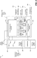
- FIG. 1 is a block diagram of a system on chip (SOC) device 100 including representative voltage islands 110 and 140 operating within different voltage ranges 120 and 150, respectively, that are centered around a common midpoint.
- the system on chip device 100 may include a semiconductor device that is fabricated to include a plurality of circuit elements grouped into a plurality of voltage islands, such as the first voltage island 110 and the second voltage island 140.
- the first voltage island 110 receives a first positive supply voltage V DD1 122 and a first negative supply voltage V SS1 124 to define the first voltage range ⁇ V 1 120 in which the first voltage island 110 is configured to operate.
- the first voltage island 110 includes one or more circuit elements 112 that operate within the first voltage range ⁇ V 1 120 to perform one or more functions.
- the second voltage island 140 receives a first positive supply voltage V DD2 152 and a first negative supply voltage V SS2 154 to define the second voltage range ⁇ V 2 150 in which the second voltage island 140 is configured to operate.
- the second voltage island 140 includes a circuit element 142, or a plurality of circuit elements (not shown in FIG. 1 ) to perform one or more additional functions, such as functions that may be based on a signal 130 output by the first voltage island 110 to the second voltage island 140.
- the signal 130 may include one of a pair of binary values (e.g., logic “1” and logic “0”), such as a high binary data value 132 (e.g., logic "1") above a threshold voltage 134 or a low binary value 136 (e.g., logic "0") below the threshold voltage 136.
- a first midpoint voltage 126 of the first voltage range ⁇ V 1 120 and a second midpoint voltage 156 of the second voltage range ⁇ V 2 150 are set to a common midpoint voltage.
- the threshold voltages recognized by the voltage islands 110 and 140 may be relatively close to the midpoint voltages 126, and 156, respectively, or, at least, the threshold voltages may be closer to the midpoint voltages 126 and 156 than to extremes of the voltage ranges 120 and 150. Thus, substantially equating the common midpoint voltages 126 and 156 may enable the second voltage island 140 to correctly interpret the data value represented by the signal 130 output by the first voltage island 110.
- the first positive supply voltage V DD1 122 may be +1.0 V and the first negative supply voltage V SS1 124 may be 0v
- the second positive supply voltage V DD2 152 may be +5.0 V and the second negative supply voltage V SS2 154 may be 0 V.
- the threshold voltage that differentiates between a high and low signal for the second voltage island 140 operating within the second voltage range ⁇ V 2 150 between V DD2 152 at +5.0 V and V SS2 154 at 0 V (e.g., a threshold of 2.5v) may exceed the first positive supply voltage V DD1 122 of +1.0 V.
- the second voltage island 140 may be unable to correctly interpret a high data value represented by the signal 130 without level translators.
- the value of the signal 130 may exceed the threshold voltage of the second voltage island 140.
- the signal 130 may be correctly interpreted by the second voltage island 140 as representing a high data value.
- the voltage ranges ⁇ V 1 120 and ⁇ V 2 150 may be substantially equated to a convenient or desired common midpoint voltage.
- the convenient or desired common midpoint voltage is 0v
- the positive supply voltages 122 and 152 and the negative supply voltages 124 and 154 may be evenly centered around 0v, as given by Eqs.
- the first positive supply voltage V DD1 122 may be +0.5 V and the first negative supply voltage V SS1 124 may be -0.5 V.
- the second positive supply voltage V DD2 152 may be +2.5 V and the second negative supply voltage V SS2 154 may be -2.5 V.
- the first voltage range ⁇ V 1 120 is 1.0 V and the second voltage range ⁇ V 2 150 is 5.0 V and the desired common midpoint voltage is -2.0 V
- the first positive supply voltage V DD1 122 would be -1.5 V and the first negative supply voltage V SS1 124 would be -2.5 V.
- the second positive supply voltage V DD2 152 would be +0.5 V and the second negative supply voltage V SS2 154 would be -4.5 V.
- the positive and negative supply voltages thus may be set for any voltage ranges and any convenient or desired common midpoint voltage.
- first voltage range ⁇ V 1 120 is 1.0 V and the second voltage range ⁇ V 2 150 is 5.0 V, and where the voltage ranges 120 and 150 are centered around a common midpoint of 0 V.
- first positive supply voltage V DD1 122 may be +0.5 V
- first negative supply voltage V SS1 124 may be -0.5 V
- second positive supply voltage V DD2 152 may be +2.5 V
- second negative supply voltage V SS2 154 may be -2.5 V.
- the signal 130 output by the first voltage island 110 represents a high data value (e.g., logical "1")
- the signal 130 is likely to be expressed as a positive voltage between the common midpoint of 0 V and the first positive supply voltage V DD1 122 of +0.5 V. Because the positive voltage of the signal 130 is likely to be closer to the second positive supply voltage V DD2 152 of +2.5 V than to the second negative supply voltage V SS2 154 of -2.5 V, the data value represented by the signal 130 is likely to exceed the threshold voltage of the second voltage island 140.
- the second voltage island 140 may correctly interpret the signal 130 as representing a high data value.
- the signal 130 output by the first voltage island 110 represents a low data value (e.g., logical "0")
- the signal 130 is likely to be expressed as a negative voltage between 0 V and the first negative supply voltage V SS1 124 of -0.5 V.
- the negative voltage of the signal 130 is likely to be closer to the second negative supply voltage V SS2 154 of -2.5 V than to the second positive supply voltage V DD2 152 of +2.5 V
- the data value represented by the signal 130 is likely to be less than the threshold voltage of the second voltage island 140.
- the second voltage island 140 may correctly interpret the signal 130 as representing a low data value.
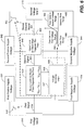
- FIG. 2 is a block diagram of a system 200 including a system on chip (SOC) device 210 with a power management controller 240 that selectively controls the voltage ranges of voltage islands 260, 262, 264 and facilitates communication of signals between the voltage islands 260, 262, 264.
- the system 200 also includes a voltage source 220.
- the voltage source 220 may be an off-chip voltage source that is external to the system on chip device 210. Alternatively, the voltage source 220 may be integrated within the system on chip device 210.
- the voltage source 220 includes a transformer 222 and tracking voltage regulators 224 that are used to provide a plurality of supply voltages 226 to the system on chip device 210.
- a plurality of positive supply voltages V DDi 228 and a plurality of negative supply voltages V SSi 230 may be provided to the power management controller 240 of the system on chip device 210.
- the power management controller 240 applies selected or converted voltage outputs 232 to the voltage islands 260, 262, 264, to registers 270, 272, and to other elements of the system on chip device 210.
- the power management controller 240 may convert voltages to lower or higher voltages as well as provide tracking regulation.
- the embodiment of FIG. 2 includes three voltage islands 260, 262, 264 separated by two registers 270, 272, but embodiments may include any number of voltage islands separated by registers.
- the supply voltages 226 supplied by the voltage source 220 also may provide one or more positive and negative supply voltages to a data input/output interface 250.
- the data input/output interface 250 may communicate with other systems that operate within different voltage ranges than the voltage ranges in which the voltage islands 260, 262, 264 of the system on chip device 210 operate.
- the voltages supplied to the data input/output interface 250 may be centered around a common midpoint in a similar manner as the other voltages supplied to the system on chip device 210 if the external devices also receive voltages centered around the common midpoint.
- the voltage source 220 may provide positive and negative supply voltages of +5.0 V and 0 V to the data input/output interface 250 even when the other supply voltages provided to the system-on-chip device 210 are centered around a common midpoint voltage whether the common midpoint voltage is 0 V or has whether the common midpoint voltage has a positive or negative non-zero voltage.
- the power management controller 240 receives the supply voltages 226 from the voltage source 220 and selectively applies the supply voltages 226 to the voltage islands 260, 262, 264 to balance considerations such as performance, heat generation, and power consumption. As previously noted, the power management controller 240 may also accommodate on-chip voltage sources instead of receiving power from an off-chip voltage source, such as the voltage source 220.
- the power management controller 240 monitors input signals, such as temperature or process measurements 282 and critical path timing signals 286 that represent performance or operating conditions of the voltage islands 260, 262, 264. The information provided by the temperature or process measurements 282 and critical path timing signals 286 is used in selectively supplying power to each of the voltage islands 260, 262, 264.
- the voltage islands 260, 262, 264 and registers 270, 272 are used to perform a series of processing operations on data received from the data input/output interface 250. After a first voltage island 260 receives input data from the data input/output interface 250 and processes the input data, an output of the first voltage island 260 may be stored by a first register 270 and passed to a second voltage island 262. After the second voltage island 262 processes the data received via the first register 270, the second voltage island 262 processes the data and an output of the second voltage island 262 is stored by a second register 272 and passed to a third voltage island 264. (As described with reference to FIG.
- the registers 270, 272 may each include one or more latches or edge-triggered flip-flops.) An output of the third voltage island 264 is received by the data input/output interface 250 and may be supplied to another system or subsystem (not shown in FIG. 2 ).
- the registers 270, 272 may store or buffer the signals passed between the voltage islands 260, 262, 264, such as when the voltage islands include asynchronous processing devices.
- the registers 270, 272 may translate voltages of the signals passed between the voltage islands 260, 262, 264.
- Operation of the voltage islands 260, 262, 264 is monitored by the power management controller 240.
- the power management controller 240 receives one or more input signals, such as temperature or process measurements 282 and critical path timing signals 286 that reflect the processing status or condition of the voltage islands 260, 262, 264.
- the power management controller 240 may determine whether more power should be supplied to one or more of the voltage islands 260, 262, 264 to increase processing performance.
- the power management controller 240 also may reduce power to one or more of the voltage islands 260, 262, 264 if processing is proceeding faster than necessary.
- the power management controller 240 also may reduce power to one or more of the voltage islands 260, 262, 264 if operating temperatures of one or more of the voltage islands 260, 262, 264 indicate that the voltage islands are operating at an excessive temperature or may be consuming excessive quantities of power.
- Temperature or process sensors 280 may be associated with one or more of the voltage islands 260, 262, 264 to monitor an operating temperature or other indicia of operating speed (e.g., one or more completion signals) to gauge the operating speed of the voltage islands 260, 262, 264.
- the temperature or process measurements 282 may be communicated from the temperature or process sensors 280 to the power management controller 240.
- the temperature or process measurements 282 may convey temperature measurements that may be used to determine if one or more of the voltage islands 260, 262, 264 are operating at acceptable or excessive temperatures or to adjust voltages to maintain temperature-sensitive timing margins.
- the temperature or process measurements 282 also may include an offset to correct for timing variations that may occur in one or more of the voltage islands 260, 262, 264 as a result of fabrication process variability.
- Critical path detection logic 284 also may be used to monitor whether significant processing tasks have been completed or to measure timing slack (i.e., a length of time between completion of a computation and latching the result with the clock) in one or more of the voltage islands 260, 262, 264 and to indicate whether power supplied to any of the voltage islands 260, 262, 264, or at intermediate points within these islands, should be increased or decreased.
- Critical path timing signals 286 are relayed by the critical path detection logic 284 to the power management controller 240. The critical path timing signals 286 are used alone or in combination with the temperature and process measurements 282 to govern the supply of power to the voltage islands 260, 262, 264.
- the positive supply voltages V DDi 228 and the negative supply voltages V SSi 230 selectively supplied to the voltage islands 260, 262, 264 are centered around a common midpoint.
- the second voltage island 262 may be able to correctly interpret the signals presented by the first voltage island 260 directly or, potentially, via the first register 270.
- the second voltage island 262 may not misinterpret a high signal generated by the first voltage island 260 as a low signal just because the supply voltages of the second voltage island 262 have a greater range than the supply voltages of the first voltage island 260. Further, when the third voltage island 264 is operating at lower positive and negative supply voltages, the third voltage island 264 will be able to correctly interpret the signals presented by the second voltage island 262 directly or via the second register 272. Using the common midpoint, the third voltage island 264 may correctly interpret a low signal generated by the second voltage island 262 (i.e., the third voltage island 264 may not incorrectly interpret the low signal generated by the second voltage island 262 as a high signal).
- FIG. 3 is a block diagram of a system 300 including a first device 310 operating within a first voltage range 321 provided by a first voltage supply 320 and a second device 350 operating within a second voltage range 361 provided by a second voltage supply 360 where the first voltage range 321 and the second voltage range 361 are centered around a common midpoint voltage 330.
- At least one of the first voltage supply 320 and the second voltage supply 360 is configured to change voltage supply levels.
- the first voltage supply 320 may be configured to change the first positive supply voltage V DD1 322 and the first negative supply voltage V SS1 324 around the common midpoint voltage 330 used as a first midpoint voltage of the first device 310.
- the second voltage supply 360 may be configured to change the second positive supply voltage V DD2 362 and the second negative supply voltage V SS2 364 around the common midpoint voltage 330 used as a second midpoint voltage of the second device 350.
- the first device 310 and the second device 350 may each include separate physical devices, and each of the devices 310 and 350 may include one or more circuit elements (not shown in FIG. 3 ).
- the first voltage range 321 between a first positive supply voltage V DD1 322 and a first negative supply voltage V SS1 324 and the second voltage range 361 between a second positive supply voltage V DD2 362 and a first negative supply voltage V SS2 364 are centered around the common midpoint voltage 330.
- a threshold voltage against which a data value represented by a signal 340 may be interpreted within both voltage ranges 321 and 361.
- the threshold voltage is relatively closer to the common midpoint voltage 330 than to the second positive supply voltage 362 or the second negative supply voltage 364, the data value carried by the signal 340 generated by the first device 310 may be correctly interpreted by the second device 350.
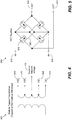
- FIG. 4 is a diagram representing a multiple-tapped transformer 400, such as the transformer 222 of FIG. 2 , from which a range of positive and negative supply voltages may be drawn around a common midpoint.
- the transformer 400 is tapped at symmetrical winding points about the common midpoint 410.
- the first voltages +V 1 420 and -V 1 422 and second voltages +V 2 430 and -V 2 432 may be centered around a common midpoint 410.
- FIG. 5 is a schematic diagram of a field effect transistor (FET) rectifier 500 used in voltage regulators such as the tracking voltage regulators 224 of FIG. 2 .
- An alternating current supply is received at input terminals 510 and 520 and the FET rectifier 500 generates a rectified, direct current at output terminals 530 and 540.
- the FET rectifier 500 uses a plurality of field effect transistors 560 along with a plurality of diodes 550 to provide a rectified direct current voltage supply at the output terminals 530 and 540.
- the FET rectifier 500 will operate at a range of midpoint voltages, such as the common midpoint of 0 V or a non-zero common midpoint voltage.
- the FET rectifier 500 is one example of a tracking voltage supply that may be included, for example, in the tracking voltage regulators 224 in the voltage source 220 of FIG. 2 .
- the FET rectifier 500 is configured to supply a rectified voltage drawn from at least one pair of a plurality of symmetrical winding taps of a transformer, such as the multiple-tapped transformer 400 of FIG. 4 .
- FIG. 6 is a block diagram of a register subsystem 600, including a master latch or master edge-triggered flip-flop 630 to receive a first signal 620 from a first voltage island 610 operating within a first voltage range to translate the first signal 620 from the first voltage range to a second signal 660 in a second voltage range.
- the register subsystem 600 also includes a slave latch or slave edge-triggered flip-flop 640 that receives the second signal 660 and presents the stored second signal 661 (derived from the second signal) to the second voltage island 670.
- the register subsystem 600 may be implemented using only a single latch or edge-triggered flip flop positioned as the master latch or master edge-triggered flip-flop 630.
- the master latch or master edge-triggered flip-flop 630 and the slave latch or slave edge-triggered flip-flop 640 will be referred to as the master latch 630 and the slave latch 640, respectively, for the rest of the description of FIG. 6 .
- the first voltage island 610 is coupled to a first positive supply voltage 632 and a first negative supply voltage 634.
- the second voltage island 670 is coupled to a second positive supply voltage 642 and a second negative supply voltage 644.
- Voltage switching logic 646 is coupled both to the first positive supply voltage 632 and the first negative supply voltage 634 and to the second positive supply voltage 642 and the second negative supply voltage 644.
- the master latch 630 (or, in a single latch or single edge-triggered flip-flop embodiment, the only latch) receives a positive supply voltage 647 that is either V DD1 or V DD2 (V DD1 /V DD2 ) and a negative supply voltage 649 that is either V SS1 or V SS2 (V SS1 /N SS2 ).
- the voltage switching logic 646 selectively supplies either V DD1 or V DD2 and either V SS1 or V SS2 as the positive supply voltage 647 and the negative supply voltage 649, respectively.
- the slave latch 640 when used, is coupled to a second positive supply voltage 642 and a second negative supply voltage 644.
- the master latch 630 receives the first signal 620 from the first voltage island 610 operating within a first voltage range between a first positive voltage supply 632 and a first negative voltage supply 634.
- the master latch 630 stores a data value represented by the first signal 620.
- the first signal 620 may have a relatively small voltage swing 622 between low and high data values, as previously described.
- the master latch 630 presents a second signal 660 which, as further described below, may have a relatively large voltage swing 662 between low and high data values to facilitate the second signal 660 being read by the second voltage island 670, as also previously described.
- the slave latch 640 receives the second signal 660 presented by the master latch 630 and stores the data value represented.
- the output of the slave latch 640 is a stored second signal 661 that corresponds to the voltage swing 662 of the second signal 660 received from the master latch 630.
- the stored second signal 661 is presented to the second voltage island 670.
- the voltage switching logic causes the master latch 630 to change operating voltages.
- the master latch 630 receives the first signal 620 while operating within the first voltage range between the first positive supply voltage 632 and the first negative supply voltage 634 provided to the master latch 630 by the voltage switching logic 646 as the positive supply voltage 647 and the negative supply voltage 649, respectively.
- the voltage switching logic 646 changes the positive supply voltage 647 and the negative supply voltage 649 to the second positive supply voltage 642 and the second negative supply voltage 644, respectively.
- the output of the master latch 630 is the second signal 660 which is presented over the larger voltage swing 662 between low and high data values.
- the second signal 660 output by the master latch 630 (and presented to the second voltage island 670 by the slave latch 640 when the slave latch 640 is used) may then represent the same data value as represented by the first signal 620 in the second voltage range within which a second voltage island 670 operates.
- the voltage ranges within which one or more of the voltage islands 610 and 670 and the latches 630 and 640 operate may be predetermined or may be controlled by an external device, such as the power management controller 240 of FIG. 2 .
- a data value in the first voltage range 690 stored in the master latch 630 during a first time period 680 may be translated to a different voltage to represent the data value in the second voltage range 692 during a second time period 682.
- the time periods 680, 682 may be adjacent or non-adjacent periods of a clock signal (not shown in FIG. 6 ) used to clock one or more devices, such as the master latch 630 and the slave latch 640.
- the data value represented by the second signal 660 may be correctly interpreted by the second voltage island 670 as the same data value represented by the first signal 620 of the first voltage island 610.
- the latch subsystem translates the data value represented by a first voltage in the first voltage range 690 to the data value represented by a second value in the second voltage domain without certain limitations of conventional voltage translators.
- the translation of the first signal 620 to the second signal 660 does not involve the use of an amplifier, thereby saving the power that may have been consumed by an amplifier.
- the latch subsystem 600 may operate synchronously with a clock signal (not shown in FIG. 6 ). Thus, operations performed at the second voltage island 670 on the second signal 660 may not have the latency due to a voltage translator.
- the master latch 630 may be receiving and translating a subsequent first signal 620 based on a subsequent data value generated by the first voltage island 610 at the same time the slave latch 640 is presenting the stored second signal 661, based on the previous second signal 660).
- the master latch 630 may be a single latch that receives the first signal 620, translates the first signal 620 to the second signal 660, and presents the second signal directly to the second voltage island 670.
- the signal voltage generated by the first voltage island 610 is being translated from a relatively small voltage range determined by the first positive supply voltage 632 and the first negative supply voltage 634 to a larger voltage range between the second positive supply voltage 642 and the second negative supply voltage 644.
- the first signal 620 has a relatively small voltage swing 622 between low and high data values as compared to the second signal 660 which has a larger voltage swing 662 between low and high data values.
- This translation may be helpful when the second voltage island 670 or another receiving device has a midpoint voltage that is greater than the high voltage of the preceding system so that a high data value signal from the first voltage island 610 is not misread as a low data value signal by the second voltage island 670.
- first voltage island 610 and the second voltage island 670 operate within voltage ranges that are centered around a common midpoint, using registers between the voltage islands 610, 670 to translate the data value signals may not be needed.
- first voltage island 610 operates within a higher voltage range than the second voltage island 670 (i.e., the opposite of the previously described example) and the voltage ranges are centered around a common midpoint, a low data value signal generated by the first voltage island 610 is likely to be below the threshold voltage of the second voltage island 670 without using registers for voltage translation.
- FIGs. 7A-7C are timing diagrams 700, 720, 740 representing how signals may be translated using different types of latch or flip-combinations as registers between voltage islands, such as the first voltage island 610 and the second voltage island 670 ( FIG. 6 ).
- a first timing diagram 700 represents an implementation using latches.
- a master latch clock signal 702 clocks a master latch, such as the master latch 630, and a slave latch clock signal 708 clocks a slave latch, such as the slave latch 640.
- the master latch stores a received signal when the master latch clock signal 702 is at a high level, such as at time t1 710. After the master latch clock signal 702 is at a low level, such as at time t2 712, the value of the data signal is stored in the master latch.
- the positive supply voltage V DD 704 and the negative supply voltage V SS 706 transition to new levels, defining a wider voltage swing as shown in FIG. 7A .
- the supply voltages V DD 704 and V SS 706 transition while the same data value is stored in the master latch, so the data value remains the same but the data value will be output according to a larger voltage swing proportional to the higher voltage range defined by the changed supply voltages V DD 704 and V SS 706 after time t3 714.
- the slave latch clock signal 708 is at a high level, causing the slave latch to store the data value presented by the output signal of the master latch. Because of the translation of the signal representing the data value to the higher voltage range at which the slave latch operates (as described with reference to FIG. 6 ), the slave latch may be better able to accurately read the data value presented by the master latch.
- the slave latch then presents the stored data value to another voltage island operating within the same voltage range as the slave latch, as described with reference to FIG. 6 .
- a second timing diagram 720 represents an implementation using positive edge-triggered flip-flops as the registers between voltage islands.
- a master flip-flop clock signal 722 clocks a master positive edge-triggered flip-flop, such as the master edge-triggered flip-flop 630, and a slave flip-flop clock signal 728 clocks a slave latch, such as the slave edge-triggered flip-flop latch 640.
- the slave flip-flop clock signal 748 may be an inverse of the master flip-flop clock signal 722 and thus a single clock source and an inverter may provide both the master flip-flop clock signal 722 and the slave flip-flop clock signal 728.
- the master flip-flop stores a received signal when the master flip-flop clock signal 722 transitions to a high level, such as at time t1' 730 (i.e., at a positive edge).
- a positive supply voltage V DD 724 and a negative supply voltage V SS 726 transition to new levels, defining a wider voltage swing as shown in FIG. 7B .
- the supply voltages V DD 724 and V SS 726 transition while the same data value is stored in the master latch, so the data value remains the same but the data value will be output according to a larger voltage swing proportional to the higher voltage range defined by the changed supply voltages V DD 724 and V SS 726 after time t2' 732.
- the slave latch clock signal 728 transitions to a high level (i.e., at a positive edge), causing the slave latch to store the data value presented by the output signal of the master latch. Because of the translation of the signal representing the data value to the higher voltage range at which the slave latch operates, the slave latch may be better able to accurately read the data value presented by the master latch. The slave latch then presents the stored data value to another voltage island operating within the same voltage range as the slave latch.
- a third timing diagram 740 represents an implementation using a positive edge-triggered master flip-flop and a negative edge-triggered flip-flop as the registers between voltage islands.
- a master flip-flop clock signal 742 clocks a master positive edge-triggered flip-flop, such as the master edge-triggered flip-flop 630, and a slave flip-flop clock signal 748 clocks a slave latch, such as the slave edge-triggered flip-flop latch 640.
- the master flip-flop clock signal 742 and the slave flip-flop clock signal 748 may be the same signal generated by a single clock source.
- the master flip-flop stores a received signal when the master flip-flop clock signal 742 transitions to a high level (i.e., at a positive edge), such as at time t1" 750.
- the master flip-flop clock signal 742 remains at a high level (or at least before another positive edge at a transition to a high level), such as at time t3" 754, while the value of the data signal remains stored in the master latch, a positive supply voltage V DD 744 and a negative supply voltage V SS 746 transition to new levels, defining a wider voltage swing as shown in FIG. 7C .
- the supply voltages V DD 744 and V SS 746 transition while the same data value is stored in the master latch, so the data value remains the same but the data value will be output according to a larger voltage swing proportional to the higher voltage range defined by the changed supply voltages V DD 744 and V SS 746 after time t2" 752.
- the slave latch clock signal 748 transitions to a low level (i.e., at a negative edge), causing the slave latch to store the data value presented by the output signal of the master latch. Because of the translation of the signal representing the data value to the higher voltage range at which the slave latch operates, the slave latch may be better able to accurately read the data value presented by the master latch. The slave latch then presents the stored data value to another voltage island operating within the same voltage range as the slave latch.
- FIG. 8 is a flow diagram of a particular embodiment of a method 800 of controlling a latch to translate a first signal representing a data value in a first voltage range to a second signal representing the data value in a second voltage range.
- the first signal within the first voltage range is received, at 802.
- the first signal may include the first signal 620 as received by the master latch 630 of FIG. 6 .
- the first signal represents a data value (e.g., logic "0" or logic "1").
- the first signal is stored in a latch operating within the first voltage range, at 804, such as the master latch 630 or a single latch operating using the first positive supply voltage 632 and the first negative supply voltage 634 of FIG. 6 .
- the latch is controlled to selectively change from operating within the first voltage range to operating within a second voltage range, at 806.
- the voltage switching logic 646 controls the master latch 630 (or a single latch) to cause the master latch 630 (or a single latch) to receive the second positive supply voltage 642 and the second negative supply voltage 644 to operate in a second voltage range.
- the second voltage range is different than the first voltage range.
- a second signal is output from the latch, at 808.
- the second signal output from the latch is comparable to the second signal 661 of FIG. 6 output by the slave latch 640.
- the second signal represents the data value of the first signal within the second voltage range.
- the second signal like the second signal 660 may be received and stored by the slave latch 640 of FIG. 6 and presented to the second voltage island 670 as the stored second signal 661. Alternatively, the second signal may be presented directly to the second voltage island 670 of FIG. 6 without using a slave latch.
Landscapes
- Engineering & Computer Science (AREA)
- Theoretical Computer Science (AREA)
- General Engineering & Computer Science (AREA)
- Physics & Mathematics (AREA)
- Computer Hardware Design (AREA)
- General Physics & Mathematics (AREA)
- Computing Systems (AREA)
- Mathematical Physics (AREA)
- Semiconductor Integrated Circuits (AREA)
- Power Sources (AREA)
- Logic Circuits (AREA)
Applications Claiming Priority (2)
| Application Number | Priority Date | Filing Date | Title |
|---|---|---|---|
| US12/636,875 US8502590B2 (en) | 2009-12-14 | 2009-12-14 | System and method of controlling devices operating within different voltage ranges |
| PCT/US2010/058938 WO2011075327A1 (en) | 2009-12-14 | 2010-12-03 | System and method of controlling devices operating within different voltage ranges |
Publications (2)
| Publication Number | Publication Date |
|---|---|
| EP2513749A1 EP2513749A1 (en) | 2012-10-24 |
| EP2513749B1 true EP2513749B1 (en) | 2019-09-18 |
Family
ID=43778397
Family Applications (1)
| Application Number | Title | Priority Date | Filing Date |
|---|---|---|---|
| EP10796209.4A Active EP2513749B1 (en) | 2009-12-14 | 2010-12-03 | System and method of controlling devices operating within different voltage ranges |
Country Status (5)
| Country | Link |
|---|---|
| US (2) | US8502590B2 (enExample) |
| EP (1) | EP2513749B1 (enExample) |
| JP (1) | JP6099398B2 (enExample) |
| CN (1) | CN102656540B (enExample) |
| WO (1) | WO2011075327A1 (enExample) |
Families Citing this family (4)
| Publication number | Priority date | Publication date | Assignee | Title |
|---|---|---|---|---|
| US8502590B2 (en) | 2009-12-14 | 2013-08-06 | The Boeing Company | System and method of controlling devices operating within different voltage ranges |
| CN103699506B (zh) * | 2012-09-27 | 2017-04-12 | 深圳市中兴微电子技术有限公司 | 一种跨电压域数据传输方法、电压域子系统和电子设备 |
| KR102190453B1 (ko) | 2014-02-17 | 2020-12-11 | 삼성전자주식회사 | 전력 관리 장치 및 이를 포함하는 시스템 온 칩 |
| US9935542B2 (en) * | 2015-03-15 | 2018-04-03 | Plsense Ltd. | Methods and apparatuses for adaptive dynamic voltage control for optimizing energy per operation per a given target speed |
Family Cites Families (36)
| Publication number | Priority date | Publication date | Assignee | Title |
|---|---|---|---|---|
| US617836A (en) * | 1899-01-17 | Mud-guard | ||
| US4626706A (en) | 1984-05-24 | 1986-12-02 | Advanced Micro Devices, Inc. | Digital signal level translation/master-slave flip flop with look-ahead |
| US5614847A (en) * | 1992-04-14 | 1997-03-25 | Hitachi, Ltd. | Semiconductor integrated circuit device having power reduction mechanism |
| JPH06188372A (ja) | 1992-07-20 | 1994-07-08 | Philips Electron Nv | 集積半導体回路 |
| JP3725911B2 (ja) * | 1994-06-02 | 2005-12-14 | 株式会社ルネサステクノロジ | 半導体装置 |
| JP3730003B2 (ja) * | 1997-02-18 | 2005-12-21 | 株式会社東芝 | 半導体装置 |
| JP3577404B2 (ja) * | 1997-08-27 | 2004-10-13 | 株式会社東芝 | 電圧レベル変換機能付ラッチ回路及びフリップフロップ回路 |
| WO2002029893A1 (fr) * | 2000-10-03 | 2002-04-11 | Hitachi, Ltd | Dispositif à semi-conducteur |
| JP2002111470A (ja) * | 2000-10-03 | 2002-04-12 | Hitachi Ltd | 半導体装置 |
| US6792582B1 (en) | 2000-11-15 | 2004-09-14 | International Business Machines Corporation | Concurrent logical and physical construction of voltage islands for mixed supply voltage designs |
| US6720673B2 (en) | 2001-04-11 | 2004-04-13 | International Business Machines Corporation | Voltage island fencing |
| JP2003168735A (ja) * | 2001-11-30 | 2003-06-13 | Hitachi Ltd | 半導体集積回路装置 |
| US6667648B2 (en) * | 2002-04-23 | 2003-12-23 | International Business Machines Corporation | Voltage island communications circuits |
| US6731154B2 (en) * | 2002-05-01 | 2004-05-04 | International Business Machines Corporation | Global voltage buffer for voltage islands |
| US6986116B2 (en) | 2003-01-07 | 2006-01-10 | International Business Machines Corporation | Signal balancing between voltage domains |
| US7091574B2 (en) | 2003-03-13 | 2006-08-15 | International Business Machines Corporation | Voltage island circuit placement |
| TWI371674B (en) * | 2003-05-07 | 2012-09-01 | Mosaid Technologies Inc | Managing power on integrated circuits using power islands |
| WO2004102628A2 (en) * | 2003-05-08 | 2004-11-25 | The Trustees Of Columbia University In The City Of New York | Examiner |
| US7131074B2 (en) * | 2003-07-08 | 2006-10-31 | International Business Machines Corporation | Nested voltage island architecture |
| US7000214B2 (en) | 2003-11-19 | 2006-02-14 | International Business Machines Corporation | Method for designing an integrated circuit having multiple voltage domains |
| US7296251B2 (en) | 2004-05-25 | 2007-11-13 | International Business Machines Corporation | Method of physical planning voltage islands for ASICs and system-on-chip designs |
| WO2005125012A1 (en) | 2004-06-15 | 2005-12-29 | Koninklijke Philips Electronics N.V. | Adaptive control of power supply for integrated circuits |
| US7382178B2 (en) * | 2004-07-09 | 2008-06-03 | Mosaid Technologies Corporation | Systems and methods for minimizing static leakage of an integrated circuit |
| JP4158922B2 (ja) * | 2004-12-20 | 2008-10-01 | インターナショナル・ビジネス・マシーンズ・コーポレーション | マイクロコンピュータ |
| US7215188B2 (en) * | 2005-02-25 | 2007-05-08 | Freescale Semiconductor, Inc. | Integrated circuit having a low power mode and method therefor |
| JP2006237388A (ja) * | 2005-02-25 | 2006-09-07 | Matsushita Electric Ind Co Ltd | 半導体集積回路及び半導体集積回路の制御方法及び信号伝送回路 |
| US20070047364A1 (en) | 2005-08-31 | 2007-03-01 | International Business Machines Corporation | Methods and apparatus for varying a supply voltage or reference voltage using independent control of diode voltage in asymmetrical double-gate devices |
| JP4777730B2 (ja) * | 2005-09-20 | 2011-09-21 | セイコーインスツル株式会社 | Dc−dcコンバータ |
| JP4858445B2 (ja) * | 2005-10-13 | 2012-01-18 | 日本電気株式会社 | 半導体ディジタル回路、fifoバッファ回路及びデータ受け渡し方法 |
| US7259590B1 (en) * | 2006-02-16 | 2007-08-21 | International Business Machines Corporation | Driver for multi-voltage island/core architecture |
| JP4829034B2 (ja) * | 2006-08-09 | 2011-11-30 | 株式会社東芝 | 半導体集積回路 |
| US7936153B2 (en) * | 2007-02-06 | 2011-05-03 | International Business Machines Corporation | On-chip adaptive voltage compensation |
| US8015426B2 (en) * | 2008-03-27 | 2011-09-06 | International Business Machines Corporation | System and method for providing voltage power gating |
| JP2009253529A (ja) * | 2008-04-03 | 2009-10-29 | Sharp Corp | ラッチ機能付きレベルシフタ回路、表示素子駆動回路および液晶表示装置 |
| DE102008049677B4 (de) * | 2008-09-30 | 2014-09-18 | Infineon Technologies Ag | Spannungsversorgung in einer Schaltungsanordnung mit einem Halbleiterschaltelement |
| US8502590B2 (en) | 2009-12-14 | 2013-08-06 | The Boeing Company | System and method of controlling devices operating within different voltage ranges |
-
2009
- 2009-12-14 US US12/636,875 patent/US8502590B2/en active Active
-
2010
- 2010-12-03 CN CN201080056786.9A patent/CN102656540B/zh active Active
- 2010-12-03 WO PCT/US2010/058938 patent/WO2011075327A1/en not_active Ceased
- 2010-12-03 EP EP10796209.4A patent/EP2513749B1/en active Active
- 2010-12-03 JP JP2012544592A patent/JP6099398B2/ja active Active
-
2013
- 2013-06-28 US US13/931,483 patent/US8860490B2/en active Active
Non-Patent Citations (1)
| Title |
|---|
| MAHMOODI-MEIMAND H ET AL: "Dual-edge triggered level converting flip-flops", 23 May 2004, PROCEEDINGS / 2004 IEEE INTERNATIONAL SYMPOSIUM ON CIRCUITS AND SYSTEMS : MAY 23 - 26, 2004, SHERATON VANCOUVER WALL CENTRE HOTEL, VANCOUVER, BRITISH COLUMBIA, CANADA, IEEE OPERATIONS CENTER, PISCATAWAY, NJ, PAGE(S) 661 - 664, ISBN: 978-0-7803-8251-0, XP010720423 * |
Also Published As
| Publication number | Publication date |
|---|---|
| WO2011075327A1 (en) | 2011-06-23 |
| US20110169543A1 (en) | 2011-07-14 |
| US8860490B2 (en) | 2014-10-14 |
| JP6099398B2 (ja) | 2017-03-22 |
| US8502590B2 (en) | 2013-08-06 |
| JP2013527941A (ja) | 2013-07-04 |
| CN102656540B (zh) | 2015-09-16 |
| EP2513749A1 (en) | 2012-10-24 |
| US20130285731A1 (en) | 2013-10-31 |
| CN102656540A (zh) | 2012-09-05 |
Similar Documents
| Publication | Publication Date | Title |
|---|---|---|
| KR101911656B1 (ko) | 전압 도메인들에 걸친 통신 방법 | |
| US7085943B2 (en) | Method and circuitry for controlling supply voltage in a data processing system | |
| US7979724B2 (en) | System and method for dynamically managing power consumption of integrated circuitry | |
| US7622954B2 (en) | Level shifter with memory interfacing two supply domains | |
| US9952651B2 (en) | Deterministic current based frequency optimization of processor chip | |
| CN105302222B (zh) | 电子装置中的功率闸控 | |
| US8405371B2 (en) | Voltage regulator with ripple compensation | |
| EP2513749B1 (en) | System and method of controlling devices operating within different voltage ranges | |
| US6700407B1 (en) | Extended voltage range level shifter | |
| CN106662902B (zh) | 用于降低集成电路功率的多域异构工艺-电压-温度跟踪 | |
| TW200925819A (en) | Self-aware adaptive power control system and a method for determining the circuit state | |
| US10018680B2 (en) | Semiconductor device, battery monitoring system, and method for activating semiconductor device | |
| CN101320729A (zh) | 半导体集成电路 | |
| EP3200351B1 (en) | Io interface level shift circuit, io interface level shift method and storage medium | |
| US20190163257A1 (en) | Apparatus for Power Consumption Reduction in Electronic Circuitry and Associated Methods | |
| US11573268B1 (en) | Skew detection system and method to remove unwanted noise due to skewed signals | |
| CN118012201B (zh) | 一种双电源域低功耗控制系统 | |
| KR100728572B1 (ko) | 반도체 메모리 장치 | |
| TW201618464A (zh) | 在一積體電路中之資料及時脈信號電壓 | |
| US10491208B2 (en) | Semiconductor device including CMOS circuit and operation method thereof | |
| CN100539368C (zh) | 使用单个引线支持ic功率输入和功率控制的电路及方法 | |
| CN114665861A (zh) | 包括功率门控电路的半导体装置 | |
| Rajeev et al. | VLSI Implementation of Level Shifter: A Review Paper | |
| CN116682469A (zh) | 用于动态辅助控制的系统级硬件机制 | |
| KR20190089695A (ko) | 로직 블록의 데이터를 유지시키기 위한 파워 게이팅 회로 |
Legal Events
| Date | Code | Title | Description |
|---|---|---|---|
| PUAI | Public reference made under article 153(3) epc to a published international application that has entered the european phase |
Free format text: ORIGINAL CODE: 0009012 |
|
| 17P | Request for examination filed |
Effective date: 20120718 |
|
| AK | Designated contracting states |
Kind code of ref document: A1 Designated state(s): AL AT BE BG CH CY CZ DE DK EE ES FI FR GB GR HR HU IE IS IT LI LT LU LV MC MK MT NL NO PL PT RO RS SE SI SK SM TR |
|
| DAX | Request for extension of the european patent (deleted) | ||
| 17Q | First examination report despatched |
Effective date: 20141202 |
|
| STAA | Information on the status of an ep patent application or granted ep patent |
Free format text: STATUS: EXAMINATION IS IN PROGRESS |
|
| GRAP | Despatch of communication of intention to grant a patent |
Free format text: ORIGINAL CODE: EPIDOSNIGR1 |
|
| STAA | Information on the status of an ep patent application or granted ep patent |
Free format text: STATUS: GRANT OF PATENT IS INTENDED |
|
| INTG | Intention to grant announced |
Effective date: 20190320 |
|
| GRAS | Grant fee paid |
Free format text: ORIGINAL CODE: EPIDOSNIGR3 |
|
| GRAJ | Information related to disapproval of communication of intention to grant by the applicant or resumption of examination proceedings by the epo deleted |
Free format text: ORIGINAL CODE: EPIDOSDIGR1 |
|
| GRAL | Information related to payment of fee for publishing/printing deleted |
Free format text: ORIGINAL CODE: EPIDOSDIGR3 |
|
| STAA | Information on the status of an ep patent application or granted ep patent |
Free format text: STATUS: EXAMINATION IS IN PROGRESS |
|
| GRAR | Information related to intention to grant a patent recorded |
Free format text: ORIGINAL CODE: EPIDOSNIGR71 |
|
| STAA | Information on the status of an ep patent application or granted ep patent |
Free format text: STATUS: GRANT OF PATENT IS INTENDED |
|
| GRAA | (expected) grant |
Free format text: ORIGINAL CODE: 0009210 |
|
| STAA | Information on the status of an ep patent application or granted ep patent |
Free format text: STATUS: THE PATENT HAS BEEN GRANTED |
|
| INTC | Intention to grant announced (deleted) | ||
| INTG | Intention to grant announced |
Effective date: 20190808 |
|
| AK | Designated contracting states |
Kind code of ref document: B1 Designated state(s): AL AT BE BG CH CY CZ DE DK EE ES FI FR GB GR HR HU IE IS IT LI LT LU LV MC MK MT NL NO PL PT RO RS SE SI SK SM TR |
|
| REG | Reference to a national code |
Ref country code: GB Ref legal event code: FG4D |
|
| REG | Reference to a national code |
Ref country code: CH Ref legal event code: EP |
|
| REG | Reference to a national code |
Ref country code: DE Ref legal event code: R096 Ref document number: 602010061133 Country of ref document: DE |
|
| REG | Reference to a national code |
Ref country code: AT Ref legal event code: REF Ref document number: 1182083 Country of ref document: AT Kind code of ref document: T Effective date: 20191015 |
|
| REG | Reference to a national code |
Ref country code: IE Ref legal event code: FG4D |
|
| REG | Reference to a national code |
Ref country code: NL Ref legal event code: MP Effective date: 20190918 |
|
| PG25 | Lapsed in a contracting state [announced via postgrant information from national office to epo] |
Ref country code: SE Free format text: LAPSE BECAUSE OF FAILURE TO SUBMIT A TRANSLATION OF THE DESCRIPTION OR TO PAY THE FEE WITHIN THE PRESCRIBED TIME-LIMIT Effective date: 20190918 Ref country code: HR Free format text: LAPSE BECAUSE OF FAILURE TO SUBMIT A TRANSLATION OF THE DESCRIPTION OR TO PAY THE FEE WITHIN THE PRESCRIBED TIME-LIMIT Effective date: 20190918 Ref country code: BG Free format text: LAPSE BECAUSE OF FAILURE TO SUBMIT A TRANSLATION OF THE DESCRIPTION OR TO PAY THE FEE WITHIN THE PRESCRIBED TIME-LIMIT Effective date: 20191218 Ref country code: LT Free format text: LAPSE BECAUSE OF FAILURE TO SUBMIT A TRANSLATION OF THE DESCRIPTION OR TO PAY THE FEE WITHIN THE PRESCRIBED TIME-LIMIT Effective date: 20190918 Ref country code: NO Free format text: LAPSE BECAUSE OF FAILURE TO SUBMIT A TRANSLATION OF THE DESCRIPTION OR TO PAY THE FEE WITHIN THE PRESCRIBED TIME-LIMIT Effective date: 20191218 Ref country code: FI Free format text: LAPSE BECAUSE OF FAILURE TO SUBMIT A TRANSLATION OF THE DESCRIPTION OR TO PAY THE FEE WITHIN THE PRESCRIBED TIME-LIMIT Effective date: 20190918 |
|
| REG | Reference to a national code |
Ref country code: LT Ref legal event code: MG4D |
|
| PG25 | Lapsed in a contracting state [announced via postgrant information from national office to epo] |
Ref country code: GR Free format text: LAPSE BECAUSE OF FAILURE TO SUBMIT A TRANSLATION OF THE DESCRIPTION OR TO PAY THE FEE WITHIN THE PRESCRIBED TIME-LIMIT Effective date: 20191219 Ref country code: RS Free format text: LAPSE BECAUSE OF FAILURE TO SUBMIT A TRANSLATION OF THE DESCRIPTION OR TO PAY THE FEE WITHIN THE PRESCRIBED TIME-LIMIT Effective date: 20190918 Ref country code: AL Free format text: LAPSE BECAUSE OF FAILURE TO SUBMIT A TRANSLATION OF THE DESCRIPTION OR TO PAY THE FEE WITHIN THE PRESCRIBED TIME-LIMIT Effective date: 20190918 Ref country code: LV Free format text: LAPSE BECAUSE OF FAILURE TO SUBMIT A TRANSLATION OF THE DESCRIPTION OR TO PAY THE FEE WITHIN THE PRESCRIBED TIME-LIMIT Effective date: 20190918 |
|
| REG | Reference to a national code |
Ref country code: AT Ref legal event code: MK05 Ref document number: 1182083 Country of ref document: AT Kind code of ref document: T Effective date: 20190918 |
|
| PG25 | Lapsed in a contracting state [announced via postgrant information from national office to epo] |
Ref country code: ES Free format text: LAPSE BECAUSE OF FAILURE TO SUBMIT A TRANSLATION OF THE DESCRIPTION OR TO PAY THE FEE WITHIN THE PRESCRIBED TIME-LIMIT Effective date: 20190918 Ref country code: NL Free format text: LAPSE BECAUSE OF FAILURE TO SUBMIT A TRANSLATION OF THE DESCRIPTION OR TO PAY THE FEE WITHIN THE PRESCRIBED TIME-LIMIT Effective date: 20190918 Ref country code: EE Free format text: LAPSE BECAUSE OF FAILURE TO SUBMIT A TRANSLATION OF THE DESCRIPTION OR TO PAY THE FEE WITHIN THE PRESCRIBED TIME-LIMIT Effective date: 20190918 Ref country code: PT Free format text: LAPSE BECAUSE OF FAILURE TO SUBMIT A TRANSLATION OF THE DESCRIPTION OR TO PAY THE FEE WITHIN THE PRESCRIBED TIME-LIMIT Effective date: 20200120 Ref country code: AT Free format text: LAPSE BECAUSE OF FAILURE TO SUBMIT A TRANSLATION OF THE DESCRIPTION OR TO PAY THE FEE WITHIN THE PRESCRIBED TIME-LIMIT Effective date: 20190918 Ref country code: IT Free format text: LAPSE BECAUSE OF FAILURE TO SUBMIT A TRANSLATION OF THE DESCRIPTION OR TO PAY THE FEE WITHIN THE PRESCRIBED TIME-LIMIT Effective date: 20190918 Ref country code: RO Free format text: LAPSE BECAUSE OF FAILURE TO SUBMIT A TRANSLATION OF THE DESCRIPTION OR TO PAY THE FEE WITHIN THE PRESCRIBED TIME-LIMIT Effective date: 20190918 Ref country code: PL Free format text: LAPSE BECAUSE OF FAILURE TO SUBMIT A TRANSLATION OF THE DESCRIPTION OR TO PAY THE FEE WITHIN THE PRESCRIBED TIME-LIMIT Effective date: 20190918 |
|
| PG25 | Lapsed in a contracting state [announced via postgrant information from national office to epo] |
Ref country code: IS Free format text: LAPSE BECAUSE OF FAILURE TO SUBMIT A TRANSLATION OF THE DESCRIPTION OR TO PAY THE FEE WITHIN THE PRESCRIBED TIME-LIMIT Effective date: 20200224 Ref country code: SK Free format text: LAPSE BECAUSE OF FAILURE TO SUBMIT A TRANSLATION OF THE DESCRIPTION OR TO PAY THE FEE WITHIN THE PRESCRIBED TIME-LIMIT Effective date: 20190918 Ref country code: CZ Free format text: LAPSE BECAUSE OF FAILURE TO SUBMIT A TRANSLATION OF THE DESCRIPTION OR TO PAY THE FEE WITHIN THE PRESCRIBED TIME-LIMIT Effective date: 20190918 Ref country code: SM Free format text: LAPSE BECAUSE OF FAILURE TO SUBMIT A TRANSLATION OF THE DESCRIPTION OR TO PAY THE FEE WITHIN THE PRESCRIBED TIME-LIMIT Effective date: 20190918 |
|
| REG | Reference to a national code |
Ref country code: DE Ref legal event code: R097 Ref document number: 602010061133 Country of ref document: DE |
|
| PLBE | No opposition filed within time limit |
Free format text: ORIGINAL CODE: 0009261 |
|
| STAA | Information on the status of an ep patent application or granted ep patent |
Free format text: STATUS: NO OPPOSITION FILED WITHIN TIME LIMIT |
|
| PG2D | Information on lapse in contracting state deleted |
Ref country code: IS |
|
| PG25 | Lapsed in a contracting state [announced via postgrant information from national office to epo] |
Ref country code: DK Free format text: LAPSE BECAUSE OF FAILURE TO SUBMIT A TRANSLATION OF THE DESCRIPTION OR TO PAY THE FEE WITHIN THE PRESCRIBED TIME-LIMIT Effective date: 20190918 Ref country code: IS Free format text: LAPSE BECAUSE OF FAILURE TO SUBMIT A TRANSLATION OF THE DESCRIPTION OR TO PAY THE FEE WITHIN THE PRESCRIBED TIME-LIMIT Effective date: 20200119 |
|
| REG | Reference to a national code |
Ref country code: CH Ref legal event code: PL |
|
| 26N | No opposition filed |
Effective date: 20200619 |
|
| REG | Reference to a national code |
Ref country code: BE Ref legal event code: MM Effective date: 20191231 |
|
| PG25 | Lapsed in a contracting state [announced via postgrant information from national office to epo] |
Ref country code: SI Free format text: LAPSE BECAUSE OF FAILURE TO SUBMIT A TRANSLATION OF THE DESCRIPTION OR TO PAY THE FEE WITHIN THE PRESCRIBED TIME-LIMIT Effective date: 20190918 Ref country code: MC Free format text: LAPSE BECAUSE OF FAILURE TO SUBMIT A TRANSLATION OF THE DESCRIPTION OR TO PAY THE FEE WITHIN THE PRESCRIBED TIME-LIMIT Effective date: 20190918 |
|
| PG25 | Lapsed in a contracting state [announced via postgrant information from national office to epo] |
Ref country code: LU Free format text: LAPSE BECAUSE OF NON-PAYMENT OF DUE FEES Effective date: 20191203 Ref country code: IE Free format text: LAPSE BECAUSE OF NON-PAYMENT OF DUE FEES Effective date: 20191203 |
|
| PG25 | Lapsed in a contracting state [announced via postgrant information from national office to epo] |
Ref country code: LI Free format text: LAPSE BECAUSE OF NON-PAYMENT OF DUE FEES Effective date: 20191231 Ref country code: CH Free format text: LAPSE BECAUSE OF NON-PAYMENT OF DUE FEES Effective date: 20191231 Ref country code: BE Free format text: LAPSE BECAUSE OF NON-PAYMENT OF DUE FEES Effective date: 20191231 |
|
| PG25 | Lapsed in a contracting state [announced via postgrant information from national office to epo] |
Ref country code: CY Free format text: LAPSE BECAUSE OF FAILURE TO SUBMIT A TRANSLATION OF THE DESCRIPTION OR TO PAY THE FEE WITHIN THE PRESCRIBED TIME-LIMIT Effective date: 20190918 |
|
| PG25 | Lapsed in a contracting state [announced via postgrant information from national office to epo] |
Ref country code: HU Free format text: LAPSE BECAUSE OF FAILURE TO SUBMIT A TRANSLATION OF THE DESCRIPTION OR TO PAY THE FEE WITHIN THE PRESCRIBED TIME-LIMIT; INVALID AB INITIO Effective date: 20101203 Ref country code: MT Free format text: LAPSE BECAUSE OF FAILURE TO SUBMIT A TRANSLATION OF THE DESCRIPTION OR TO PAY THE FEE WITHIN THE PRESCRIBED TIME-LIMIT Effective date: 20190918 |
|
| PG25 | Lapsed in a contracting state [announced via postgrant information from national office to epo] |
Ref country code: TR Free format text: LAPSE BECAUSE OF FAILURE TO SUBMIT A TRANSLATION OF THE DESCRIPTION OR TO PAY THE FEE WITHIN THE PRESCRIBED TIME-LIMIT Effective date: 20190918 |
|
| PG25 | Lapsed in a contracting state [announced via postgrant information from national office to epo] |
Ref country code: MK Free format text: LAPSE BECAUSE OF FAILURE TO SUBMIT A TRANSLATION OF THE DESCRIPTION OR TO PAY THE FEE WITHIN THE PRESCRIBED TIME-LIMIT Effective date: 20190918 |
|
| P01 | Opt-out of the competence of the unified patent court (upc) registered |
Effective date: 20230516 |
|
| PGFP | Annual fee paid to national office [announced via postgrant information from national office to epo] |
Ref country code: GB Payment date: 20241227 Year of fee payment: 15 |
|
| PGFP | Annual fee paid to national office [announced via postgrant information from national office to epo] |
Ref country code: FR Payment date: 20241226 Year of fee payment: 15 |
|
| PGFP | Annual fee paid to national office [announced via postgrant information from national office to epo] |
Ref country code: DE Payment date: 20241227 Year of fee payment: 15 |