EP2511806A2 - Capacitive touch switch - Google Patents
Capacitive touch switch Download PDFInfo
- Publication number
- EP2511806A2 EP2511806A2 EP12004387A EP12004387A EP2511806A2 EP 2511806 A2 EP2511806 A2 EP 2511806A2 EP 12004387 A EP12004387 A EP 12004387A EP 12004387 A EP12004387 A EP 12004387A EP 2511806 A2 EP2511806 A2 EP 2511806A2
- Authority
- EP
- European Patent Office
- Prior art keywords
- electrodes
- lines
- substrate
- touch switch
- auxiliary
- Prior art date
- Legal status (The legal status is an assumption and is not a legal conclusion. Google has not performed a legal analysis and makes no representation as to the accuracy of the status listed.)
- Withdrawn
Links
Images









Classifications
-
- G—PHYSICS
- G06—COMPUTING OR CALCULATING; COUNTING
- G06F—ELECTRIC DIGITAL DATA PROCESSING
- G06F3/00—Input arrangements for transferring data to be processed into a form capable of being handled by the computer; Output arrangements for transferring data from processing unit to output unit, e.g. interface arrangements
- G06F3/01—Input arrangements or combined input and output arrangements for interaction between user and computer
- G06F3/03—Arrangements for converting the position or the displacement of a member into a coded form
- G06F3/041—Digitisers, e.g. for touch screens or touch pads, characterised by the transducing means
- G06F3/044—Digitisers, e.g. for touch screens or touch pads, characterised by the transducing means by capacitive means
-
- H—ELECTRICITY
- H03—ELECTRONIC CIRCUITRY
- H03K—PULSE TECHNIQUE
- H03K17/00—Electronic switching or gating, i.e. not by contact-making and –breaking
- H03K17/94—Electronic switching or gating, i.e. not by contact-making and –breaking characterised by the way in which the control signals are generated
- H03K17/96—Touch switches
- H03K17/962—Capacitive touch switches
- H03K17/9622—Capacitive touch switches using a plurality of detectors, e.g. keyboard
-
- G—PHYSICS
- G06—COMPUTING OR CALCULATING; COUNTING
- G06F—ELECTRIC DIGITAL DATA PROCESSING
- G06F3/00—Input arrangements for transferring data to be processed into a form capable of being handled by the computer; Output arrangements for transferring data from processing unit to output unit, e.g. interface arrangements
- G06F3/01—Input arrangements or combined input and output arrangements for interaction between user and computer
- G06F3/03—Arrangements for converting the position or the displacement of a member into a coded form
- G06F3/041—Digitisers, e.g. for touch screens or touch pads, characterised by the transducing means
- G06F3/044—Digitisers, e.g. for touch screens or touch pads, characterised by the transducing means by capacitive means
- G06F3/0446—Digitisers, e.g. for touch screens or touch pads, characterised by the transducing means by capacitive means using a grid-like structure of electrodes in at least two directions, e.g. using row and column electrodes
-
- G—PHYSICS
- G06—COMPUTING OR CALCULATING; COUNTING
- G06F—ELECTRIC DIGITAL DATA PROCESSING
- G06F3/00—Input arrangements for transferring data to be processed into a form capable of being handled by the computer; Output arrangements for transferring data from processing unit to output unit, e.g. interface arrangements
- G06F3/01—Input arrangements or combined input and output arrangements for interaction between user and computer
- G06F3/03—Arrangements for converting the position or the displacement of a member into a coded form
- G06F3/041—Digitisers, e.g. for touch screens or touch pads, characterised by the transducing means
- G06F3/044—Digitisers, e.g. for touch screens or touch pads, characterised by the transducing means by capacitive means
- G06F3/0445—Digitisers, e.g. for touch screens or touch pads, characterised by the transducing means by capacitive means using two or more layers of sensing electrodes, e.g. using two layers of electrodes separated by a dielectric layer
-
- G—PHYSICS
- G06—COMPUTING OR CALCULATING; COUNTING
- G06F—ELECTRIC DIGITAL DATA PROCESSING
- G06F2203/00—Indexing scheme relating to G06F3/00 - G06F3/048
- G06F2203/041—Indexing scheme relating to G06F3/041 - G06F3/045
- G06F2203/04103—Manufacturing, i.e. details related to manufacturing processes specially suited for touch sensitive devices
-
- G—PHYSICS
- G06—COMPUTING OR CALCULATING; COUNTING
- G06F—ELECTRIC DIGITAL DATA PROCESSING
- G06F2203/00—Indexing scheme relating to G06F3/00 - G06F3/048
- G06F2203/041—Indexing scheme relating to G06F3/041 - G06F3/045
- G06F2203/04112—Electrode mesh in capacitive digitiser: electrode for touch sensing is formed of a mesh of very fine, normally metallic, interconnected lines that are almost invisible to see. This provides a quite large but transparent electrode surface, without need for ITO or similar transparent conductive material
Definitions
- the present invention relates to a planar body and a touch switch.
- a touch switch is arranged at the front side of the display device, and a touch position is detected.
- the types of touch switches include a resistive type, a surface acoustic wave type, an infrared type, and the like.
- Patent Literature 1 discloses a capacitive touch switch having a matrix electrode (a two-layer structure in X-direction and Y-direction), as shown in Figs. 19 and 20 .
- a known capacitive touch switch 400 comprises a first planar body 403 having a substrate 401 and transparent first electrodes 402 comprising ITO, and arranged in a strip pattern on one side of the substrate 401; and a second planar body 406 having a substrate 404 and transparent second electrodes 405 comprising ITO, and arranged in a strip pattern on one side of the substrate 404.
- the first planar body 403 and the second planar body 406 are bonded via an adhesive layer 407 in such a manner that the first electrodes and second electrodes face each other.
- the electrodes 402 and 405 detect a change in the voltage or the like based on the capacitance of a human body at the contact position, and a coordinate of the contact position is thereby calculated.
- the resistivity of ITO is high, usually 200 ⁇ / ⁇ to 1000 ⁇ / ⁇ . This results in an increase in the size of the touch switch, along with an increase in the resistance between terminals of the electrodes. This reduces the detection sensitivity of the capacitance, and disables the operation of the touch switch.
- Patent Literature 2 discloses a capacitive touch switch that does not use ITO.
- a copper or copper-alloy electrode is formed in a mesh pattern, thereby allowing the transmission of the electrode to be 70% or higher.
- a lowresistance electrode is formed while maintaining the visibility.
- Patent Literature 2 are only provided on one side of the substrate.
- the visibility will be reduced when the first planar body is overlapped with the second planar body.
- An object of the present invention is to provide a touch switch having two ITO-free electrode layers bonded together, wherein the touch switch has good visibility; and to provide a planar body that forms such a touch switch.
- a planar body including a mesh-like electrode formed in a mesh shape with multiple conductor lines on one side of a substrate, in which the mesh-like electrode is separated into multiple conductive areas disposed at intervals and non-conductive areas each disposed between the conductive areas; each non-conductive area has multiple cutting portions that cut the conductor lines, and each non-conductive area insulates between the adjacent conductive areas by the cutting portions.
- the cutting portions are preferably formed at intersections of the conductor lines of the mesh-like electrode.
- the mesh pitch of the mesh-like electrode is preferably 100 ⁇ m to 1,000 ⁇ m.
- the conductive areas preferably have multiple cutting portions that cut the conductor lines without interfering with the conductivity between the ends of each conductive area.
- a capacitive touch switch including the multiple planar bodies, in which the planar bodies are bonded together via an adhesive layer.
- the conductive areas formed on one planar body are preferably disposed to perpendicularly intersect the conductive areas formed on a different planar body.
- a touch switch including a substrate; multiple first electrodes formed on one side of the substrate and arranged at certain intervals; and multiple second electrodes formed on the other side of the substrate and arranged at certain intervals to form a grid pattern with the multiple first electrodes, in which each of the first and second electrodes forms a mesh structure with multiple conductor lines, and the direction of the conductor lines is inclined with respect to a black matrix in a display device.
- the above-described touch switch includes first auxiliary lines formed between the first electrodes on the one side of the substrate; and second auxiliary lines formed between the second electrodes on the other side thereof; in which a grid pattern with equal intervals is preferably formed by the conductor lines of the first electrodes, the first auxiliary lines, the conductor lines of the second electrodes, and the second auxiliary lines.
- the conductor lines of the first electrodes, the first auxiliary lines, or both of them formed on the one side of the substrate form continuous lines with the conductor lines of the second electrodes, the second auxiliary lines, or both of them formed on the other side of the substrate.
- a touch switch including a first substrate; a second substrate disposed facing the first substrate; multiple first electrodes formed on the first substrate, specifically on a side facing the second substrate, and arranged at certain intervals; and multiple second electrodes formed on the second substrate, specifically on a side away from the first substrate, and arranged at certain intervals to form a grid pattern with the multiple first electrodes, in which each of the first and second electrodes form a mesh structure with multiple conductor lines, and the direction of the conductor lines is inclined with respect to a black matrix in a display device.
- the touch switch includes first auxiliary lines formed between the first electrodes on the first substrate, specifically on the side facing the second substrate; and second auxiliary lines formed between the second electrodes on the second substrate, specifically on the side away from the first substrate, in which a grid pattern with equal intervals is preferably formed by the conductor lines of the first electrodes, the first auxiliary lines, the conductor lines of the second electrodes, and the second auxiliary lines.
- the conductor lines of the first electrodes, the first auxiliary lines, or both of them formed on the first substrate form continuous lines with the conductor lines of the second electrodes, the second auxiliary lines, or both of them formed on the second substrate.
- the present invention provides a touch switch having two ITO-free electrode layers bonded to each other, wherein the touch switch has good visibility; and also provides a planar body that forms such a touch switch.
- the touch switch is a capacitive touch switch mounted to a front side of a display device.
- a black matrix forming a grid pattern of horizontal and vertical lines is formed in the display device.
- a touch switch 10 shown in Fig. 1 includes a substrate 12, first electrodes 14 formed on one side of the substrate 12, and second electrodes 16 formed on the other side of the substrate 12.
- the "one side” of the substrate 12 is an upper side
- the "other side” of the substrate 12 is a lower side, which is mounted to a display device 18.
- the substrate 12 is a dielectric substrate.
- materials of the substrate 12 include transparent materials such as glass, polyester, polyethylene terephthalate, polycarbonate, polymethylmethacrylate, polyethylene naphthalate, etc.
- the thickness is about 0.1 to 2 mm.
- the thickness is about 10 to 2,000 ⁇ m.
- the first electrodes 14 and the second electrodes 16 are all arranged at certain intervals.
- the first electrodes 14 and the second electrodes 16 are oriented in mutually perpendicularly intersecting directions.
- the first electrodes 14 and the second electrodes 16 form a grid pattern.
- Each of the first electrodes 14 and second electrodes 16 has multiple conductor lines, and forms a mesh structure with the conductor lines.
- the conductor lines include long lines 20a and 20b, and multiple short lines 22a and 22b that intersect the long lines 20a and 20b.
- the long lines 20a and 20b and the short lines 22a and 22b are all disposed inclined with respect to the black matrix in the display device 18. This is because a moiré pattern would easily occur if the conductor lines and the black matrix were oriented in the same direction.
- the long lines 20a and 20b curve at certain positions.
- the angle of the curve is the same at each position.
- the angle of the curve is an angle (bias angle) at which a moiré pattern does not occur along the vertical or horizontal axis of the display device 18.
- the long lines 20a of the first electrodes 14 and the short lines 22b of the second electrodes 16 are oriented in the same direction, and the short lines 22a of the first electrodes 14 and the long lines 20b of the second electrodes 16 are oriented in the same direction.
- the line width of the long lines 20a and 20b and the short lines 22a and 22b is, for example, about 10 to 30 ⁇ m.
- the pitch of the long lines 20a and 20b is about 200 to 400 ⁇ m. Because the line width is very thin and the pitch is sufficiently large relative to the line width, the electrodes 14 and 16 are inconspicuous and unlikely to degrade the display quality level of the display device 18.
- rhombuses as shown in Fig. 4 are formed by the first electrodes 14 and the second electrodes 16.
- the grid pattern forms rhombuses rather than squares.
- the angle of the curves of the long lines 20a and 20b is suitably selected according to the size of the display device 18 and the like. Because of the curves, the conductor lines are not formed in the same direction as the black matrix. Consequently, first auxiliary lines 24 and second auxiliary lines 26, which are described below, are also disposed inclined with respect to the black matrix.
- the volume resistivity of the electrodes constituting the first electrodes 14 and the second electrodes 16 is 0.5x10⁻⁵ to 5 ⁇ 10-5 ⁇ cm, which is lower than that of ITO. Further, the volume resistivity, line width, and height are adjusted in such a manner that the resistance between terminals of electrodes 16x and 14y is 5 k ⁇ or less, preferably 1 k ⁇ or less.
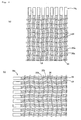
- the short lines 22a and 22b are arranged at greater intervals than the long lines 20a and 20b, and each second electrode 16 is arranged between the adjacent short lines 22a of the first electrodes 14. Further, each first electrode 14 is arranged between the adjacent short lines 22b of the second electrodes 16.
- the conductor lines such as the short lines 22a of the first electrodes 14 and the long lines 20b of the second electrodes 16 are arranged at equal intervals.
- the conductor lines such as the short lines 20a of the first electrodes 14 and the long lines 22b of the second electrodes 16 are arranged at equal intervals.
- the short lines 22a of the first electrodes 14 do not overlap with the second electrodes 16, thereby preventing the occurrence of a moiré pattern.
- the short lines 22b of the second electrodes 16 do not overlap with the first electrodes 14, thereby preventing the occurrence of a moiré pattern.
- the first electrodes 14 and the second electrodes 16 are printed with ink containing conductive nanoparticles.
- the conductive nanoparticles include silver, gold, platinum, palladium, copper, carbon, or mixtures thereof.
- the average particle size of the nanoparticles is 2 ⁇ m or smaller, preferably in a range of 200 to 500 nm. The particle size thereof is smaller than that of known micron particles. Even if the line width of the electrodes 14 and 16 is 100 ⁇ m or less, the electrodes 14 and 16 having conductivity can be formed because the particle size of the nanoparticles is sufficiently smaller than the line width of the electrodes 14 and 16. Polyester resin and the like are used as the binders of the ink.
- the amount of the binder used is 1 to 20 weight parts, preferably 3 to 10 weight parts, per 100 weight parts of the conductive nanoparticles.
- a preferable solvent of the ink is one that adequately disperses conductive nanoparticles and has a boiling point of about 100°C to 300°C. An example thereof is toluene having a boiling point of 110°C. Because the boiling point of the solvent is relatively low, the substrate 12 can be fired at a relatively low temperature after the ink is printed on the substrate 12, thereby reducing the thermal load on the substrate.
- the ink has been subject to dispersion treatment for nanoparticles.
- Material of the electrodes 14 and 16 do not include ITO containing indium, which is a rare element. Accordingly, it is possible to lower the cost of the electrode materials.
- the present invention includes the multiple first auxiliary lines 24 and the multiple second auxiliary lines 26.
- the first auxiliary lines 24 are formed on the one side of the substrate 12, and the second auxiliary lines 26 are formed on the other side of the substrate 12.
- Each first auxiliary line 24 is formed between the adjacent first electrodes 14, and each second auxiliary line 26 is formed between the adjacent second electrodes 16.
- Materials of the first auxiliary lines 24 and the second auxiliary lines 26 are the same as those of the first electrodes 14 and the like.
- the first auxiliary lines 24 and the second auxiliary lines 26 are not connected to either first electrodes 14 or second electrodes 16.
- Fig. 4 shows an enlarged view of the electrodes 14 and 16, and the auxiliary lines 24 and 26.
- the white solid lines are the first electrodes 14 and the first auxiliary lines 24 formed on the one side of the substrate 12, and the black solid lines are the second electrodes 16 and the second auxiliary lines 26 formed on the other side of the substrate 12.
- the first auxiliary lines 24 are oriented in the same direction as the short lines 22b of the second electrodes 16, and the length of the first auxiliary line 24 is equal to an interval d2 between the adjacent second electrodes 16.
- the second auxiliary lines 26 are oriented in the same direction as the short lines 20a of the second electrodes 14, and the length of the second auxiliary lines 26 is equal to an interval d1 between the adjacent first electrodes 14.
- Each first auxiliary line 24 and each second auxiliary line 26 mutually intersect at their centers.
- the first auxiliary lines 24 form continuous lines with the short lines 22b of the second electrodes 16.
- the first auxiliary lines 24 are formed on the one side of the substrate 12, and the short line 22b of the second electrodes 16 are formed on the other side thereof. Therefore, these lines are not actually in contact with each other; they are, however, arranged to form seemingly continuous lines.
- the second auxiliary lines 26 and the short line 22a of the first electrodes 14 are also arranged to form continuous lines.
- the long lines 20a of the first electrodes 14, the first auxiliary lines 24, and the short lines 22b of the second electrodes 16 are arranged at equal intervals.
- the long lines 20b of the second electrodes 16, the second auxiliary lines 26, and the short lines 22a of the first electrodes 14 are arranged at equal intervals.
- the equally spaced arrangement of these lines results in the formation of a grid with the first electrodes 14 and the like.
- these lines are seemingly continuous lines with curves at certain positions, and can form a grid pattern with the electrodes 14 and 16.
- One grid pattern is formed with the first electrodes 14 and the second electrodes 16 formed on two separate sides; it is not the case that two grid patterns are overlapped with each other to seemingly form one grid pattern.
- the present invention can prevent the occurrence of such a moiré pattern.
- the seemingly connected lines are formed, and these lines are arranged at equal intervals.
- the conductor lines in a grid pattern are formed in the touch switch 10 as shown in Fig. 3 .
- a grid pattern is formed when the first electrodes 14 and the second electrodes 16 are overlapped with each other.
- the present invention is different from prior Patent Literature 2. Even if the positions of the first electrodes 14 and the like are somewhat dislocated, the grid pattern is only slightly deformed, and a moiré pattern does not easily occur. It is possible to improve the manufacturing yield, compared to the case where the electrodes disclosed in Patent Literature 2 are arranged on both sides of the substrate.
- An acrylic transparent adhesive 28 is used to bond a cover film 30 to the one side of the substrate 12.
- the first electrodes 14 and the first auxiliary lines 24 are protected by the cover film 30.
- the one side of the substrate 12 may be coated with a transparent resin, rather than using the cover film 30.
- An acrylic transparent adhesive 32 is used to bond the other side of the substrate 12 to a front surface of the display device 18.
- the electrodes 14 and 16 have the terminals 14y and 16x at their ends, and lead wires (not shown) extend from the terminals 14y and 16x for connection.
- the lead wires are connected to a control circuit for detecting the voltage applied to the electrodes 14 and 16 and a touch position.
- a touch position is detected by applying a predetermined voltage to the electrodes 14 and 16, and detecting an electrical change that occurs when a finger is moved closer to the touch switch 10.
- a method for manufacturing the touch switch 10 is described: (1) The above-described substrate 12 and ink are provided. The substrate 12 is cut as needed into a desired shape, and washed. (2) The first electrodes 14 and the first auxiliary lines 24 are formed by printing the ink on the one side of the substrate 12. (3) The second electrodes 16 and the second auxiliary lines 26 are formed by printing the ink on the other side of the substrate 12. (4) The acrylic transparent adhesive 28 is applied to the one side of the substrate 12, and the cover film 30 is then bonded to the one side of the substrate 12.
- the printing in (2) and (3) is carried out by screen printing or ink-jet printing.
- the ink still has a high specific resistance and no conductivity after simply carrying out screen printing or ink-jet printing. Conductivity is imparted to the ink by firing the ink in a kiln after printing.
- the electrodes 14 and 16 can be very easily produced without the need for vacuum film formation and etching, which are required for the manufacturing of ITO.
- the lead wires are formed using silver ink and the like so as to extend from the end of each of the electrodes 14 and 16, and the electrodes 14 and 16 are connected to the control circuit of the touch switch via the lead wires.
- the lead wires By forming the lead wires by screen printing and the like using the same ink used for the electrodes, it is possible to simultaneously form the lead wires and the electrodes 14 and 16.
- the completed touch switch 10 is mounted to the front side of the display device 18 using the acrylic transparent adhesive 32 or the like. Alignment marks are provided, if necessary, to the corners of the substrate 12 and the display device 18 for positioning.
- a touch switch 10b shown in Fig. 5 includes a first substrate 12a, a second substrate 12b disposed facing the first substrate 12a, the multiple first electrodes 14 formed on a first side of the first substrate 12a, and the multiple second electrodes 16 formed on a first side of the second substrate 12b.
- the first side of the first substrate 12a faces a second side of the second substrate 12b.
- the first side of the second substrate 12b is a side mounted to the display device 18.
- the first electrodes 14 and the second electrodes 16 are the same as those shown in Figs. 2 to 4 . They are mesh-like electrodes formed by the long lines 20a and 20b, and the short lines 22a and 22b. Materials for the substrates 12a and 12b and the electrodes 14 and 16 are the same as those for the touch switch 10.
- the first auxiliary lines 24 are formed on the first side of the first substrate 12a, and the second auxiliary lines 26 are formed on the first side of the second substrate 12b. Each first auxiliary line 24 is formed between the adjacent first electrodes 14, and each second auxiliary line 26 is formed between the adjacent second electrodes 16.
- the first auxiliary lines 24 are oriented in the same direction as the short lines 22b of the second electrodes 16, and the length of each first auxiliary line 24 is equal to an interval d2 between the adjacent second electrodes 16.
- the second auxiliary lines 26 are oriented in the same direction as the short lines 22a of the second electrodes 14, and the length of each second auxiliary line 26 is equal to an interval d1 between the adjacent first electrodes 14. Materials for the first auxiliary lines 24 and the second auxiliary lines 26 are the same as those for the first electrodes 14 and the like.
- the first auxiliary lines 24 form continuous lines with the short lines 22b of the second electrodes 16. These lines are not in contact with each other; they are, however, arranged to form seemingly continuous lines. Likewise, the second auxiliary lines 26 and the short lines 20a of the first electrodes 14 are also arranged to form continuous lines.
- the first substrate 12a and the second substrate 12b are bonded to each other using a transparent acrylic transparent adhesive 34 or the like.
- the second substrate 12b and the second electrodes 16 are bonded to the display device 18 using a transparent acrylic transparent adhesive 36 or the like.
- lead wires are connected to the terminals 14y and 16x of the electrodes 14 and 16.
- the lead wires are connected to a control circuit that detects the voltage applied to the electrodes 14 and 16, and a touch position.
- a touch position is detected by applying a predetermined voltage to the electrodes 14 and 16, and detecting an electrical change that occurs when a finger is moved closer to the touch switch 10b.
- a method for manufacturing the touch switch 10b is described: (1) The above-described substrate 12 and ink are provided. The substrates 12a and 12b are cut as needed into a desired shape, and washed. (2) The first electrodes 14 and the first auxiliary lines 24 are formed by printing the ink on the first side of the substrate 12a. (3) The second electrodes 16 and the second auxiliary lines 26 are formed by printing the ink on the first side of the second substrate 12b. (4) The first substrate 12a and the second substrate 12b are bonded to each other using the acrylic transparent adhesive 34, in such a manner that the second side of the second substrate 12b is disposed facing the first side of the first substrate 12a.
- the printing in (2) and (3) is carried out by screen printing or ink-jet printing.
- the printing can be performed very easily.
- Conductivity is imparted to the ink by firing the ink in a kiln after printing.
- the completed touch switch 10b is mounted to the front side of the display device 18 using the acrylic transparent adhesive 36 or the like.
- the touch switches 10 and 10b of the present invention have the auxiliary lines 24 each formed between the adjacent electrodes 14, and the auxiliary lines 26 each formed between the adjacent electrodes 16.
- a grid pattern with equal intervals is formed by these electrodes 14 and the like, and a moiré pattern does not easily occur.
- a grid pattern of electrodes is not formed only on one side of the substrate, as in Patent Literature 2, but is formed using both sides of the substrate. A moiré pattern does not easily occur even if the positional accuracy of the electrodes 14 and the like is decreased, and the manufacturing yield can be improved.
- the first electrodes 14 and the first auxiliary lines 24 may be formed on the surface of the display device 18, viewing the display device 18 as the first substrate ( Fig. 6 ).
- the second electrodes 16 and the second auxiliary lines 26 are formed on one side of a second substrate 12c, and the other side of the second substrate 12c is bonded to the display device 18 using an acrylic transparent adhesive 38.
- the cover film 30 is bonded to the one side of the second substrate 12c using the acrylic transparent adhesive 28, thereby protecting the second electrodes 16 and the second auxiliary lines 26.
- the first electrodes 14, the first auxiliary lines 24, the second electrodes 16, the second auxiliary lines 26, the second substrate 12c, and the like have the same structures as those in the above-described embodiment.
- Electrodes 14b and second electrodes 16b in which multiple meshes are put together, as shown in Figs. 7(a) and (b) , may be used.
- the first electrodes 14b and the second electrodes 16b are arranged at equal intervals.
- Each first auxiliary line 24b is provided and connected between the adjacent first electrodes 14b.
- Each second auxiliary line 26b is provided and connected between the adjacent second electrodes 16b.
- the first electrodes 14b and the second electrodes 16b are respectively disposed on the one side and the other side of the substrate 12 of Fig. 1 , or are respectively disposed on the first substrate 12a and the second substrate 12b of Fig. 5 .
- a grid pattern as shown in Fig. 8 is formed.
- the electrodes 16x and the electrodes 14y are directly or indirectly connected to the ends of the first electrodes 14b and the ends of the second electrodes 16b, respectively.
- a moiré pattern does not easily occur.
- the conductor lines and the auxiliary lines are inclined at 45 degrees with respect to the black matrix.
- the angle of inclination is adjusted to an angle at which a moiré pattern does not easily occur, according to the display device that is actually used.
- the structures of the electrodes 14 and 16 and the auxiliary lines 24 and 26 described in Fig. 2 and the like are merely examples.
- the important points are: (1) the conductor lines and the like are inclined with respect to the black matrix in the display device; (2) a grid pattern is formed using the substrate 12, with the conductor lines and the like formed on both sides of one substrate 12, or on the two substrates 12a and 12b; and (3) the conductor lines and the like may intersect each other when a grid pattern is formed, but they do not overlap each other.
- electrodes e shown in Fig. 9 were formed with ITO as well as with mesh-like silver electrodes. Each electrode e has a width of 3 mm and a length of 30 cm. In the case of the ITO, the resistance between the patterns of the electrodes e was about 30 k ⁇ . In the case of the silver electrodes, the resistance was about 52 ⁇ .
- a comparison of the sensitivity was performed using the seventh electrode e from the top. A predetermined voltage was applied from a terminal y at the left end of the electrode e, and a change in the capacitance was also detected from the terminal y. The sensitivity was substantially the same at point O, which is 0 cm from the terminal y.
- the sensitivity of the ITO electrode was 1/3 that of the mesh-like silver electrode at point P, which is 15 cm away from the terminal y; and 1/5 at point Q, which is 30 cm away from the terminal y.
- a change in the sensitivity from points O to Q was very small.
- the sensitivity was very small at points P (15 cm) and Q (30 cm). This shows that the size of the touch switch of the present invention can be easily enlarged, compared to the case where the ITO electrode is used.
- Fig. 10 is an enlarged schematic cross-sectional diagram of the main components of a touch switch according to a second embodiment of the present invention.
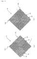
- This touch switch 105 is a capacitive touch switch, and includes, as shown in Figs. 11 and 12 , a first planar body 101 in which a mesh-like electrode 112 is formed on one side of a substrate 111, and a second planar body 102 in which a mesh-like electrode 122 is formed on one side of a substrate 121.
- Fig. 11 is a plan view of the first planar body 101
- Fig. 12 is a plan view of the second planar body 102.
- the first planar body 101 and the second planar body 102 are integrally bonded via an adhesive layer 103 in such a manner that the mesh-like electrodes 112 and 122 on their respective planar bodies face each other.
- the first planar body 101 and the second planar body 102 are bonded in such a manner that conductive areas 112a of the first planar body 101 and conductive areas 122a of the second planar body 102, which are described below, perpendicularly intersect each other.
- the substrates 111 and 121 are dielectric substrates.
- materials of the substrates 111 and 121 include transparent materials such as glass, polyester, polyethylene terephthalate, polycarbonate, polymethylmethacrylate, polyethylene naphthalate, etc.
- the thickness is preferably about 0.1 to 3 mm; in the case of plastic film, the thickness is preferably about 10 to 2,000 ⁇ m. These materials may also be laminated in multiple layers.
- the mesh-like electrodes 112 and 122 respectively formed on one side of the first planar body 101 and on one side of the second planar body 102 are electrodes formed in a mesh pattern with multiple conductor lines L.
- the mesh-like electrode 112 (122) is separated into the multiple conductive areas 112a (122a) disposed substantially parallel to each other at predetermined intervals, and non-conductive areas 112b (122b) each disposed between the adjacent conductive areas.
- Fig. 14 is a diagram showing boundaries between the conductive areas 112a and the non-conductive areas 112b of Fig. 11 .
- Fig. 15 is a diagram showing boundaries between the conductive areas 122a and the non-conductive areas 122b of Fig. 12 .
- the gray colored portion represents the conductive areas 112a and 122a.
- the conductive areas 112a and 122a are connected to an outside drive circuit (not shown) via a routed circuit (not shown) formed of conductive ink, etc.
- each non-conductive area 112b (122b) includes multiple cutting portions 104 that cut the conductor lines L into island-like forms. Each non-conductive area 112b (122b) insulates between the adjacent conductive areas by the cutting portions 104.
- the cutting portions 104 are formed at intersections of the multiple conductor lines L that form the mesh-like electrodes 112 and 122.
- the cutting width of the cutting portions 104 is, for example, about the same as the line width of the conductor lines L, or about a few times greater than the line width of the conductor lines L.
- the non-conductive areas 112b and 122b have the cutting portions 104 that cut the conductor lines L.
- This structure can ensure insulation in the non-conductive areas 112b and 122b of the mesh-like electrodes 112 and 122. Accordingly, when the touch switch 105 is formed by overlapping the first planar body 101 and the second planar body 102, the non-conductive areas 112b (122b) of the mesh-like electrode 112 (122) of the first planar body 101 (the second planar body 102) is prevented from adversely affecting the sensing of the mesh-like electrode 122 (112) of the other planar body, and thus the detection of capacitance can be stably performed.
- the line width of the conductor lines L is, for example, 10 to 30 ⁇ m.
- the pitch of the conductor lines L is 100 to 1,000 ⁇ m.
- the thickness of the conductor lines L is usually about 1 to 30 ⁇ m.
- the conductor lines L are preferably as thin as possible.
- the thickness is preferably about 10 to 30 ⁇ m.
- the mesh-like electrodes 112 and 122 having the above-described dimensions are inconspicuous because the line width of the conductor lines L is very thin, and the pitch is sufficiently large relative to the line width.
- Examples of methods for forming the conductor lines L that form the mesh-like electrodes 112 and 122 include: (i) a method in which a conductive paste containing ultrafine conductive particles is screen-printed on a transparent substrate (see Japanese Unexamined Patent Publication No. 2007-142334 , and the like); and (ii) a method in which metal foil such as copper or the like is laminated on a transparent substrate, a resist pattern is formed on the metal foil, and the metal foil is etched (see Japanese Unexamined Patent Publication No. 2008-32884 , and the like).
- the methods for forming the conductor lines L are not limited to the above described formation methods (i) and (ii). Printing methods other than the method (i), such as gravure printing, or photolithography other than the method (ii) may be used.
- the shape of the conductive areas 112a and 122a in the mesh-like electrodes 112 and 122 is formed from linearly connected multiple rhombuses.
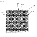
- the rhombic conductive areas of each conductive area 112a and the rhombic conductive areas of each conductive area 122a are connected in the directions in which they intersect each other; and, as shown in Fig. 16 , they are arranged in such a manner that the rhombuses of the conductive areas 112a and the rhombuses of the conductive areas 122a, which are arranged at the upper and lower sides, do not overlap each other when the first planar body 101 and the second planar body 102 are overlapped with each other.
- the shape of the conductive areas 112a and 122a can be any shape, such as a linear shape, etc., insofar as the contact point of the finger or the like can be detected.
- the first planar body 101 and the second planar body 102 are preferably bonded to each other with the adhesive layer 103 entirely interposed therebetween so as to avoid formation of an air layer.
- Epoxy-based, acryl-based and like generally used transparent adhesives may be used as the adhesive layer 103, and they may include a core material formed from a transparent film of norbornene-based resin.
- the thickness of the adhesive layer 103 is, for example, preferably 500 ⁇ m or less.
- the adhesive layer 103 may also be formed by overlapping multiple sheet-like adhesives, or by overlapping several different types of sheet-like adhesives.
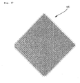
- a mesh pattern with an entirely uniform appearance is obtained as shown in Fig. 17 when the first planar body 101 and the second planar body 102 are bonded to each other in such a manner, for example, that the vertex of each mesh of the mesh-like electrode 122 on the second planar body 102 is positioned at the center of each mesh of the mesh-like electrode 112 on the first planar body 101, and the conductor lines L forming the meshes of the mesh-like electrode 112 intersect the conductor lines L forming the meshes of the mesh-like electrode 122.
- Fig. 17 is a view showing the electrodes of Figs. 13(a) and 13(b) bonded to each other.
- the touch switch 105 formed by bonding the first planar body 101 and the second planar body 102 to each other is used by being mounted, for example, to a display device in which a black matrix is formed.
- the touch switch 105 is mounted to the display device in such a manner that the mesh patterns of the conductive areas 112a and 122a and the non-conductive areas 112b and 122b are inclined with respect to the black matrix, so as to avoid a moiré pattern that occurs when the black matrix and the mesh pattern are arranged in the same direction.
- the angle of inclination is suitably adjusted to an angle at which a moiré pattern does not easily occur, according to the display device that is actually used.
- the method for detecting a touch position in the touch switch 105 having the above-described structure is the same as that in known capacitive touch switches.
- a change in the voltage based on the capacitance of a human body is detected at the contact position on the electrodes 112 and 122, and a coordinate of the contact position is thereby calculated.
- the touch switch 105 includes the mesh-like electrodes 112 and 122 respectively formed on the first planar body 101 and the second planar body 102, in which the mesh-like electrode 112 (122) is separated into the strip-like conductive areas 112a (122a), and the strip-like non-conductive areas 112b (122b) having the multiple cutting portions 104 that intermittently cut the conductor lines L. Consequently, the touch switch 105 can effectively suppress the occurrence of variation in mesh density when the first planar body 101 and the second planar body 102 are overlapped with each other, while ensuring electrical insulation in the non-conductive areas 112b and 122b. Because the variation in mesh density can be suppressed, the shape of the pattern of the mesh-like electrodes 112 and 122 can be made inconspicuous, thus improving the visibility.
- the mesh-like electrodes 112 and 122 according to the present embodiment can be printed with ink containing conductive nanoparticles, using a mask having a predetermined mask pattern. Consequently, the first planar body 101 and the second planar body 102 can be efficiently manufactured.
- the cutting portions 104 formed in the non-conductive areas 112b and 122b respectively included in the mesh-like electrodes 112 and 122 are disposed at the intersections of the multiple conductor lines L; however, the cutting portions 104 may be disposed at any positions insofar as insulation in the non-conductive areas 112b and 122b is ensured, and the length of the cutting portions 104 may also be arbitrarily set.
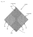
- the above-described embodiment is formed in such a manner that the only non-conductive areas 112b and 122b have the cutting portions 104 that cut the conductor lines L; however, as shown in Fig. 18 , the conductive areas 112a and 122a may be partially provided with cutting portions 104a that cut the conductor lines L insofar as they do not interfere with the conductivity between the ends 221 and 222 (321 and 322) of each conductive area 112a (122a). The visibility can be further improved by the above-described structure.
Landscapes
- Engineering & Computer Science (AREA)
- General Engineering & Computer Science (AREA)
- Theoretical Computer Science (AREA)
- Human Computer Interaction (AREA)
- Physics & Mathematics (AREA)
- General Physics & Mathematics (AREA)
- Position Input By Displaying (AREA)
- Electronic Switches (AREA)
- Switches That Are Operated By Magnetic Or Electric Fields (AREA)
Abstract
a substrate;
multiple first electrodes formed on one side of the substrate and arranged at certain intervals; and
multiple second electrodes formed on the other side of the substrate and arranged at certain intervals to form a grid pattern with the multiple first electrodes,
wherein each of the first and second electrodes forms a mesh structure with multiple conductor lines,
the touch switch comprises first auxiliary lines formed between the first electrodes on the one side, and second auxiliary lines formed between the second electrodes on the other side, and
a grid pattern with equal intervals is formed by the conductor lines of the first electrodes, the first auxiliary lines, the conductor lines of the second electrodes, and the second auxiliary lines.
Description
- The present invention relates to a planar body and a touch switch.
- These days, in the field of computers and electronic devices, operations performed using the contents displayed on a display device, rather than using buttons, have been increasingly developed. To perform such operations, a touch switch is arranged at the front side of the display device, and a touch position is detected. The types of touch switches include a resistive type, a surface acoustic wave type, an infrared type, and the like. There is also a capacitive type, in which a position is detected by a variation in capacitance caused by a touch of a finger and/or proximity of a finger. For example, Patent Literature 1 discloses a capacitive touch switch having a matrix electrode (a two-layer structure in X-direction and Y-direction), as shown in
Figs. 19 and 20 . - A detailed description is provided with reference to
Fig. 21 , which is a schematic plan diagram schematically showing the structure of a capacitive touch switch as described above; andFig. 22 , which is a cross-sectional view of the structure.
A knowncapacitive touch switch 400 comprises a firstplanar body 403 having asubstrate 401 and transparentfirst electrodes 402 comprising ITO, and arranged in a strip pattern on one side of thesubstrate 401; and a secondplanar body 406 having a substrate 404 and transparentsecond electrodes 405 comprising ITO, and arranged in a strip pattern on one side of the substrate 404. The firstplanar body 403 and the secondplanar body 406 are bonded via anadhesive layer 407 in such a manner that the first electrodes and second electrodes face each other. - When an arbitrary position on the planar body is touched with a finger or the like, the
electrodes - However, the resistivity of ITO is high, usually 200Ω/□ to 1000Ω/□. This results in an increase in the size of the touch switch, along with an increase in the resistance between terminals of the electrodes. This reduces the detection sensitivity of the capacitance, and disables the operation of the touch switch.
- Further,
Patent Literature 2 discloses a capacitive touch switch that does not use ITO. A copper or copper-alloy electrode is formed in a mesh pattern, thereby allowing the transmission of the electrode to be 70% or higher. A lowresistance electrode is formed while maintaining the visibility. - However, the electrodes in
Patent Literature 2 are only provided on one side of the substrate. When two layers of electrodes are formed using the first electrodes and the second electrodes, as described in Patent Literature 1, the visibility will be reduced when the first planar body is overlapped with the second planar body. -
- PLT 1: Japanese Unexamined Patent Publication No.
2006-511879 - PLT 2: Japanese Unexamined Patent Publication No.
2006-344163 - An object of the present invention is to provide a touch switch having two ITO-free electrode layers bonded together, wherein the touch switch has good visibility; and to provide a planar body that forms such a touch switch.
- The above-described object of the present invention is achieved by a planar body including a mesh-like electrode formed in a mesh shape with multiple conductor lines on one side of a substrate, in which the mesh-like electrode is separated into multiple conductive areas disposed at intervals and non-conductive areas each disposed between the conductive areas; each non-conductive area has multiple cutting portions that cut the conductor lines, and each non-conductive area insulates between the adjacent conductive areas by the cutting portions.
- In this planar body, the cutting portions are preferably formed at intersections of the conductor lines of the mesh-like electrode.
- Further, the mesh pitch of the mesh-like electrode is preferably 100 µm to 1,000 µm.
- Further, the conductive areas preferably have multiple cutting portions that cut the conductor lines without interfering with the conductivity between the ends of each conductive area.
- The above-described object of the present invention is also achieved by a capacitive touch switch including the multiple planar bodies, in which the planar bodies are bonded together via an adhesive layer.
- Further, in this touch switch, the conductive areas formed on one planar body are preferably disposed to perpendicularly intersect the conductive areas formed on a different planar body.
- The above-described object of the present invention is also achieved by a touch switch including a substrate; multiple first electrodes formed on one side of the substrate and arranged at certain intervals; and multiple second electrodes formed on the other side of the substrate and arranged at certain intervals to form a grid pattern with the multiple first electrodes, in which each of the first and second electrodes forms a mesh structure with multiple conductor lines, and the direction of the conductor lines is inclined with respect to a black matrix in a display device.
- The above-described touch switch includes first auxiliary lines formed between the first electrodes on the one side of the substrate; and second auxiliary lines formed between the second electrodes on the other side thereof; in which a grid pattern with equal intervals is preferably formed by the conductor lines of the first electrodes, the first auxiliary lines, the conductor lines of the second electrodes, and the second auxiliary lines.
- Further, the conductor lines of the first electrodes, the first auxiliary lines, or both of them formed on the one side of the substrate form continuous lines with the conductor lines of the second electrodes, the second auxiliary lines, or both of them formed on the other side of the substrate.
- The above-described object of the present invention is also achieved by a touch switch including a first substrate; a second substrate disposed facing the first substrate; multiple first electrodes formed on the first substrate, specifically on a side facing the second substrate, and arranged at certain intervals; and multiple second electrodes formed on the second substrate, specifically on a side away from the first substrate, and arranged at certain intervals to form a grid pattern with the multiple first electrodes, in which each of the first and second electrodes form a mesh structure with multiple conductor lines, and the direction of the conductor lines is inclined with respect to a black matrix in a display device.
- The touch switch includes first auxiliary lines formed between the first electrodes on the first substrate, specifically on the side facing the second substrate; and second auxiliary lines formed between the second electrodes on the second substrate, specifically on the side away from the first substrate, in which a grid pattern with equal intervals is preferably formed by the conductor lines of the first electrodes, the first auxiliary lines, the conductor lines of the second electrodes, and the second auxiliary lines.
- Further, the conductor lines of the first electrodes, the first auxiliary lines, or both of them formed on the first substrate form continuous lines with the conductor lines of the second electrodes, the second auxiliary lines, or both of them formed on the second substrate.
- The present invention provides a touch switch having two ITO-free electrode layers bonded to each other, wherein the touch switch has good visibility; and also provides a planar body that forms such a touch switch.
-
- [
Fig. 1] Fig. 1 shows a partial cross section of a touch switch according to a first embodiment of the present invention. - [
Fig. 2] Fig. 2 shows electrodes and auxiliary lines of the touch switch.Fig. 2(a) shows first electrodes and first auxiliary lines, andFig. 2(b) shows second electrodes and second auxiliary lines. - [
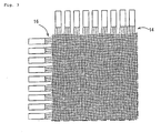
Fig. 3] Fig. 3 shows a positional relationship of the first electrodes, the first auxiliary lines, the second electrodes, and the second auxiliary lines. - [
Fig. 4] Fig. 4 is a partially enlarged view ofFig. 3 . - [
Fig. 5] Fig. 5 shows a partial cross section of the touch switch. - [
Fig. 6] Fig. 6 shows a partial cross section of the touch switch. - [
Fig. 7] Fig. 7 shows electrodes and auxiliary lines of the touch switch.Fig. 7(a) shows first electrodes and first auxiliary lines, andFig. 7(b) shows second electrodes and second auxiliary lines. - [
Fig. 8] Fig. 8 shows a positional relationship of the first electrodes, the first auxiliary lines, the second electrodes, and the second auxiliary lines ofFig. 7 . - [
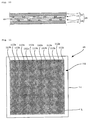
Fig. 9] Fig. 9 shows electrodes used for comparison between mesh-like electrodes and ITO electrodes. - [
Fig. 10] Fig. 10 is a schematic cross-sectional diagram of the main components of a touch switch according to a second embodiment of the present invention. - [
Fig. 11] Fig. 11 is a plan view of a first planar body included in the touch switch shown inFig. 10 . - [
Fig. 12] Fig. 12 is a plan view of a second planar body included in the touch switch shown inFig. 10 . - [
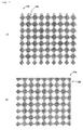
Fig. 13] Fig. 13(a) is an enlarged view of the main parts ofFig. 11 , andFig. 13(b) is an enlarged view of the main parts ofFig. 12 . - [
Fig. 14] Fig. 14 is a diagram showing boundaries between conductive areas and non-conductive areas of a mesh-like electrode of the first planar body shown inFig. 11 . - [
Fig. 15] Fig. 15 is a diagram showing boundaries between conductive areas and non-conductive areas of a mesh-like electrode of the second planar body shown inFig. 12 . - [
Fig. 16] Fig. 16 is a plan view of a touch switch according to an embodiment of the present invention. - [
Fig. 17] Fig. 17 is a plan view showing a form in which the first planar body and the second planar body are bonded to each other. - [
Fig. 18] Fig. 18 is a plan view showing a modification of the planar body of the present invention. - [
Fig. 19] Fig. 19 is a plan view of a known capacitive touch switch having a matrix electrode. - [
Fig. 20] Fig. 20 is a plan view of a known capacitive touch switch having a matrix electrode. - [
Fig. 21] Fig. 21 is a schematic plan diagram schematically showing a known capacitive touch switch. - [
Fig. 22] Fig. 22 is a cross-sectional view ofFig. 21 . - A touch switch according to a first embodiment of the present invention is described with reference to the drawings. The touch switch is a capacitive touch switch mounted to a front side of a display device. A black matrix forming a grid pattern of horizontal and vertical lines is formed in the display device.
- A
touch switch 10 shown inFig. 1 includes asubstrate 12,first electrodes 14 formed on one side of thesubstrate 12, andsecond electrodes 16 formed on the other side of thesubstrate 12. In the description, the "one side" of thesubstrate 12 is an upper side, and the "other side" of thesubstrate 12 is a lower side, which is mounted to adisplay device 18. - The
substrate 12 is a dielectric substrate. Examples of materials of thesubstrate 12 include transparent materials such as glass, polyester, polyethylene terephthalate, polycarbonate, polymethylmethacrylate, polyethylene naphthalate, etc. In the case of glass, the thickness is about 0.1 to 2 mm. In the case of plastic film, the thickness is about 10 to 2,000 µm. - As shown in
Fig. 2 , thefirst electrodes 14 and thesecond electrodes 16 are all arranged at certain intervals. Thefirst electrodes 14 and thesecond electrodes 16 are oriented in mutually perpendicularly intersecting directions. As shown inFig. 3 , thefirst electrodes 14 and thesecond electrodes 16 form a grid pattern. - Each of the
first electrodes 14 andsecond electrodes 16 has multiple conductor lines, and forms a mesh structure with the conductor lines. The conductor lines includelong lines short lines long lines long lines short lines display device 18. This is because a moiré pattern would easily occur if the conductor lines and the black matrix were oriented in the same direction. - The
long lines display device 18. Thelong lines 20a of thefirst electrodes 14 and theshort lines 22b of thesecond electrodes 16 are oriented in the same direction, and theshort lines 22a of thefirst electrodes 14 and thelong lines 20b of thesecond electrodes 16 are oriented in the same direction. The line width of thelong lines short lines long lines electrodes display device 18. - Note that rhombuses as shown in
Fig. 4 are formed by thefirst electrodes 14 and thesecond electrodes 16. In the present description, the grid pattern forms rhombuses rather than squares. The angle of the curves of thelong lines display device 18 and the like. Because of the curves, the conductor lines are not formed in the same direction as the black matrix. Consequently, firstauxiliary lines 24 and secondauxiliary lines 26, which are described below, are also disposed inclined with respect to the black matrix. - Further, because of the mesh pattern, even if one of the
long lines short lines long lines short lines first electrodes 14 and thesecond electrodes 16 is 0.5x10⁻⁵ to 5×10⁻⁵Ω·cm, which is lower than that of ITO. Further, the volume resistivity, line width, and height are adjusted in such a manner that the resistance between terminals ofelectrodes - The
short lines long lines second electrode 16 is arranged between the adjacentshort lines 22a of thefirst electrodes 14. Further, eachfirst electrode 14 is arranged between the adjacentshort lines 22b of thesecond electrodes 16. The conductor lines such as theshort lines 22a of thefirst electrodes 14 and thelong lines 20b of thesecond electrodes 16 are arranged at equal intervals. The conductor lines such as theshort lines 20a of thefirst electrodes 14 and thelong lines 22b of thesecond electrodes 16 are arranged at equal intervals. Theshort lines 22a of thefirst electrodes 14 do not overlap with thesecond electrodes 16, thereby preventing the occurrence of a moiré pattern. Also, theshort lines 22b of thesecond electrodes 16 do not overlap with thefirst electrodes 14, thereby preventing the occurrence of a moiré pattern. - The
first electrodes 14 and thesecond electrodes 16 are printed with ink containing conductive nanoparticles. The conductive nanoparticles include silver, gold, platinum, palladium, copper, carbon, or mixtures thereof. The average particle size of the nanoparticles is 2 µm or smaller, preferably in a range of 200 to 500 nm. The particle size thereof is smaller than that of known micron particles. Even if the line width of theelectrodes electrodes electrodes substrate 12 can be fired at a relatively low temperature after the ink is printed on thesubstrate 12, thereby reducing the thermal load on the substrate. The ink has been subject to dispersion treatment for nanoparticles. Material of theelectrodes - The present invention includes the multiple first
auxiliary lines 24 and the multiple secondauxiliary lines 26. The firstauxiliary lines 24 are formed on the one side of thesubstrate 12, and the secondauxiliary lines 26 are formed on the other side of thesubstrate 12. Each firstauxiliary line 24 is formed between the adjacentfirst electrodes 14, and each secondauxiliary line 26 is formed between the adjacentsecond electrodes 16. Materials of the firstauxiliary lines 24 and the secondauxiliary lines 26 are the same as those of thefirst electrodes 14 and the like. The firstauxiliary lines 24 and the secondauxiliary lines 26 are not connected to eitherfirst electrodes 14 orsecond electrodes 16. -
Fig. 4 shows an enlarged view of theelectrodes auxiliary lines first electrodes 14 and the firstauxiliary lines 24 formed on the one side of thesubstrate 12, and the black solid lines are thesecond electrodes 16 and the secondauxiliary lines 26 formed on the other side of thesubstrate 12. The firstauxiliary lines 24 are oriented in the same direction as theshort lines 22b of thesecond electrodes 16, and the length of the firstauxiliary line 24 is equal to an interval d2 between the adjacentsecond electrodes 16. Further, the secondauxiliary lines 26 are oriented in the same direction as theshort lines 20a of thesecond electrodes 14, and the length of the secondauxiliary lines 26 is equal to an interval d1 between the adjacentfirst electrodes 14. Each firstauxiliary line 24 and each secondauxiliary line 26 mutually intersect at their centers. - When the
touch switch 10 is viewed from above or below, the firstauxiliary lines 24 form continuous lines with theshort lines 22b of thesecond electrodes 16. The firstauxiliary lines 24 are formed on the one side of thesubstrate 12, and theshort line 22b of thesecond electrodes 16 are formed on the other side thereof. Therefore, these lines are not actually in contact with each other; they are, however, arranged to form seemingly continuous lines. Likewise, the secondauxiliary lines 26 and theshort line 22a of thefirst electrodes 14 are also arranged to form continuous lines. Further, thelong lines 20a of thefirst electrodes 14, the firstauxiliary lines 24, and theshort lines 22b of thesecond electrodes 16 are arranged at equal intervals. Thelong lines 20b of thesecond electrodes 16, the secondauxiliary lines 26, and theshort lines 22a of thefirst electrodes 14 are arranged at equal intervals. The equally spaced arrangement of these lines results in the formation of a grid with thefirst electrodes 14 and the like. As described above, these lines are seemingly continuous lines with curves at certain positions, and can form a grid pattern with theelectrodes first electrodes 14 and thesecond electrodes 16 formed on two separate sides; it is not the case that two grid patterns are overlapped with each other to seemingly form one grid pattern. When two grid patterns are overlapped with each other, even a slight displacement causes a moiré pattern to appear; however, the present invention can prevent the occurrence of such a moiré pattern. - As described above, the seemingly connected lines are formed, and these lines are arranged at equal intervals. As a result, the conductor lines in a grid pattern are formed in the
touch switch 10 as shown inFig. 3 . A grid pattern is formed when thefirst electrodes 14 and thesecond electrodes 16 are overlapped with each other. In this point, the present invention is different fromprior Patent Literature 2. Even if the positions of thefirst electrodes 14 and the like are somewhat dislocated, the grid pattern is only slightly deformed, and a moiré pattern does not easily occur. It is possible to improve the manufacturing yield, compared to the case where the electrodes disclosed inPatent Literature 2 are arranged on both sides of the substrate. - An acrylic
transparent adhesive 28 is used to bond acover film 30 to the one side of thesubstrate 12. Thefirst electrodes 14 and the firstauxiliary lines 24 are protected by thecover film 30. The one side of thesubstrate 12 may be coated with a transparent resin, rather than using thecover film 30. An acrylictransparent adhesive 32 is used to bond the other side of thesubstrate 12 to a front surface of thedisplay device 18. Theelectrodes terminals terminals electrodes electrodes touch switch 10. - A method for manufacturing the
touch switch 10 is described: (1) The above-describedsubstrate 12 and ink are provided. Thesubstrate 12 is cut as needed into a desired shape, and washed. (2) Thefirst electrodes 14 and the firstauxiliary lines 24 are formed by printing the ink on the one side of thesubstrate 12. (3) Thesecond electrodes 16 and the secondauxiliary lines 26 are formed by printing the ink on the other side of thesubstrate 12. (4) The acrylictransparent adhesive 28 is applied to the one side of thesubstrate 12, and thecover film 30 is then bonded to the one side of thesubstrate 12. - The printing in (2) and (3) is carried out by screen printing or ink-jet printing. The ink still has a high specific resistance and no conductivity after simply carrying out screen printing or ink-jet printing. Conductivity is imparted to the ink by firing the ink in a kiln after printing. The
electrodes - Further, the lead wires are formed using silver ink and the like so as to extend from the end of each of the
electrodes electrodes electrodes - The completed
touch switch 10 is mounted to the front side of thedisplay device 18 using the acrylic transparent adhesive 32 or the like. Alignment marks are provided, if necessary, to the corners of thesubstrate 12 and thedisplay device 18 for positioning. - Next, a different type of touch switch is described. Descriptions of the same components as in the above-described touch switch may be omitted.
- A
touch switch 10b shown inFig. 5 includes afirst substrate 12a, asecond substrate 12b disposed facing thefirst substrate 12a, the multiplefirst electrodes 14 formed on a first side of thefirst substrate 12a, and the multiplesecond electrodes 16 formed on a first side of thesecond substrate 12b. The first side of thefirst substrate 12a faces a second side of thesecond substrate 12b. The first side of thesecond substrate 12b is a side mounted to thedisplay device 18. Thefirst electrodes 14 and thesecond electrodes 16 are the same as those shown inFigs. 2 to 4 . They are mesh-like electrodes formed by thelong lines short lines substrates electrodes touch switch 10. - The first
auxiliary lines 24 are formed on the first side of thefirst substrate 12a, and the secondauxiliary lines 26 are formed on the first side of thesecond substrate 12b. Each firstauxiliary line 24 is formed between the adjacent
first electrodes 14, and each secondauxiliary line 26 is formed between the adjacentsecond electrodes 16. The firstauxiliary lines 24 are oriented in the same direction as theshort lines 22b of thesecond electrodes 16, and the length of each firstauxiliary line 24 is equal to an interval d2 between the adjacentsecond electrodes 16. Further, the secondauxiliary lines 26 are oriented in the same direction as theshort lines 22a of thesecond electrodes 14, and the length of each secondauxiliary line 26 is equal to an interval d1 between the adjacentfirst electrodes 14. Materials for the firstauxiliary lines 24 and the secondauxiliary lines 26 are the same as those for thefirst electrodes 14 and the like. - As with the above-described
touch switch 10, the firstauxiliary lines 24 form continuous lines with theshort lines 22b of thesecond electrodes 16. These lines are not in contact with each other; they are, however, arranged to form seemingly continuous lines. Likewise, the secondauxiliary lines 26 and theshort lines 20a of thefirst electrodes 14 are also arranged to form continuous lines. - As shown in
Fig. 5 , thefirst substrate 12a and thesecond substrate 12b are bonded to each other using a transparent acrylic transparent adhesive 34 or the like. Thesecond substrate 12b and thesecond electrodes 16 are bonded to thedisplay device 18 using a transparent acrylic transparent adhesive 36 or the like. - Additionally, lead wires (not shown) are connected to the
terminals electrodes electrodes electrodes touch switch 10b. - A method for manufacturing the
touch switch 10b is described: (1) The above-describedsubstrate 12 and ink are provided. Thesubstrates first electrodes 14 and the firstauxiliary lines 24 are formed by printing the ink on the first side of the substrate 12a. (3) Thesecond electrodes 16 and the secondauxiliary lines 26 are formed by printing the ink on the first side of the second substrate 12b. (4) Thefirst substrate 12a and thesecond substrate 12b are bonded to each other using the acrylictransparent adhesive 34, in such a manner that the second side of thesecond substrate 12b is disposed facing the first side of thefirst substrate 12a. - The printing in (2) and (3) is carried out by screen printing or ink-jet printing. The printing can be performed very easily. Conductivity is imparted to the ink by firing the ink in a kiln after printing. The completed
touch switch 10b is mounted to the front side of thedisplay device 18 using the acrylic transparent adhesive 36 or the like. - As described above, the touch switches 10 and 10b of the present invention have the
auxiliary lines 24 each formed between theadjacent electrodes 14, and theauxiliary lines 26 each formed between theadjacent electrodes 16. A grid pattern with equal intervals is formed by theseelectrodes 14 and the like, and a moiré pattern does not easily occur. Further, a grid pattern of electrodes is not formed only on one side of the substrate, as inPatent Literature 2, but is formed using both sides of the substrate. A moiré pattern does not easily occur even if the positional accuracy of theelectrodes 14 and the like is decreased, and the manufacturing yield can be improved. - An embodiment of the present invention is described above; however, the embodiment of the present invention is not limited to the above-described embodiment. For example, the
first electrodes 14 and the firstauxiliary lines 24 may be formed on the surface of thedisplay device 18, viewing thedisplay device 18 as the first substrate (Fig. 6 ). Thesecond electrodes 16 and the secondauxiliary lines 26 are formed on one side of asecond substrate 12c, and the other side of thesecond substrate 12c is bonded to thedisplay device 18 using an acrylictransparent adhesive 38. Thecover film 30 is bonded to the one side of thesecond substrate 12c using the acrylictransparent adhesive 28, thereby protecting thesecond electrodes 16 and the secondauxiliary lines 26. Thefirst electrodes 14, the firstauxiliary lines 24, thesecond electrodes 16, the secondauxiliary lines 26, thesecond substrate 12c, and the like have the same structures as those in the above-described embodiment. - First,
electrodes 14b andsecond electrodes 16b, in which multiple meshes are put together, as shown inFigs. 7(a) and (b) , may be used. Thefirst electrodes 14b and thesecond electrodes 16b are arranged at equal intervals. Each firstauxiliary line 24b is provided and connected between the adjacentfirst electrodes 14b. Each secondauxiliary line 26b is provided and connected between the adjacentsecond electrodes 16b. Thefirst electrodes 14b and thesecond electrodes 16b are respectively disposed on the one side and the other side of thesubstrate 12 ofFig. 1 , or are respectively disposed on thefirst substrate 12a and thesecond substrate 12b ofFig. 5 . When the first and second electrodes are overlapped with each other in the same manner as described above, a grid pattern as shown inFig. 8 is formed. In the same manner as shown inFig. 2 , theelectrodes 16x and theelectrodes 14y (not shown) are directly or indirectly connected to the ends of thefirst electrodes 14b and the ends of thesecond electrodes 16b, respectively. As shown inFigs. 7 and8 , when a grid pattern is formed and the lines forming the grid pattern are inclined with respect to the black matrix, a moiré pattern does not easily occur. - In the case as shown in
Fig. 8 , the conductor lines and the auxiliary lines are inclined at 45 degrees with respect to the black matrix. However, depending on the display device, there are cases where a moiré pattern occurs when the lines are inclined at 45 degrees. Therefore, the angle of inclination is adjusted to an angle at which a moiré pattern does not easily occur, according to the display device that is actually used. - The structures of the
electrodes auxiliary lines Fig. 2 and the like are merely examples. The important points are: (1) the conductor lines and the like are inclined with respect to the black matrix in the display device; (2) a grid pattern is formed using thesubstrate 12, with the conductor lines and the like formed on both sides of onesubstrate 12, or on the twosubstrates - In order to confirm the effect of the present invention, electrodes e shown in
Fig. 9 were formed with ITO as well as with mesh-like silver electrodes. Each electrode e has a width of 3 mm and a length of 30 cm. In the case of the ITO, the resistance between the patterns of the electrodes e was about 30 kΩ. In the case of the silver electrodes, the resistance was about 52 Ω. A comparison of the sensitivity was performed using the seventh electrode e from the top. A predetermined voltage was applied from a terminal y at the left end of the electrode e, and a change in the capacitance was also detected from the terminal y. The sensitivity was substantially the same at point O, which is 0 cm from the terminal y. The sensitivity of the ITO electrode was 1/3 that of the mesh-like silver electrode at point P, which is 15 cm away from the terminal y; and 1/5 at point Q, which is 30 cm away from the terminal y. In the case of the mesh-like silver electrode, a change in the sensitivity from points O to Q was very small. In the case of the ITO electrode, the sensitivity was very small at points P (15 cm) and Q (30 cm). This shows that the size of the touch switch of the present invention can be easily enlarged, compared to the case where the ITO electrode is used. - The present invention can be practiced in embodiments to which various improvements, modifications, and changes are added based on the knowledge of a person skilled in the art, without departing from the scope of the invention.
- Hereinbelow, a second embodiment of the present invention is described with reference to the attached drawings. Note that none of the drawings reflects the actual size. They are partially enlarged or reduced in order to facilitate the understanding of the structures.
-
Fig. 10 is an enlarged schematic cross-sectional diagram of the main components of a touch switch according to a second embodiment of the present invention. Thistouch switch 105 is a capacitive touch switch, and includes, as shown inFigs. 11 and12 , a firstplanar body 101 in which a mesh-like electrode 112 is formed on one side of asubstrate 111, and a secondplanar body 102 in which a mesh-like electrode 122 is formed on one side of asubstrate 121. Note thatFig. 11 is a plan view of the firstplanar body 101, andFig. 12 is a plan view of the secondplanar body 102. The firstplanar body 101 and the secondplanar body 102 are integrally bonded via anadhesive layer 103 in such a manner that the mesh-like electrodes planar body 101 and the secondplanar body 102 are bonded in such a manner thatconductive areas 112a of the firstplanar body 101 andconductive areas 122a of the secondplanar body 102, which are described below, perpendicularly intersect each other. - The
substrates substrates - As shown in
Figs. 11 and12 , and their enlarged viewsFigs. 13(a) and 13(b) (showing the main parts), the mesh-like electrodes planar body 101 and on one side of the secondplanar body 102 are electrodes formed in a mesh pattern with multiple conductor lines L. - Further, the mesh-like electrode 112 (122) is separated into the multiple
conductive areas 112a (122a) disposed substantially parallel to each other at predetermined intervals, andnon-conductive areas 112b (122b) each disposed between the adjacent conductive areas.Fig. 14 is a diagram showing boundaries between theconductive areas 112a and thenon-conductive areas 112b ofFig. 11 .Fig. 15 is a diagram showing boundaries between theconductive areas 122a and thenon-conductive areas 122b ofFig. 12 . In both drawings, the gray colored portion represents theconductive areas conductive areas - Further, each
non-conductive area 112b (122b) includes multiple cuttingportions 104 that cut the conductor lines L into island-like forms. Eachnon-conductive area 112b (122b) insulates between the adjacent conductive areas by the cuttingportions 104. In the present embodiment, the cuttingportions 104 are formed at intersections of the multiple conductor lines L that form the mesh-like electrodes portions 104 is, for example, about the same as the line width of the conductor lines L, or about a few times greater than the line width of the conductor lines L. - As described above, the
non-conductive areas portions 104 that cut the conductor lines L. This structure can ensure insulation in thenon-conductive areas like electrodes touch switch 105 is formed by overlapping the firstplanar body 101 and the secondplanar body 102, thenon-conductive areas 112b (122b) of the mesh-like electrode 112 (122) of the first planar body 101 (the second planar body 102) is prevented from adversely affecting the sensing of the mesh-like electrode 122 (112) of the other planar body, and thus the detection of capacitance can be stably performed. - The line width of the conductor lines L is, for example, 10 to 30 µm. The pitch of the conductor lines L is 100 to 1,000 µm. The thickness of the conductor lines L is usually about 1 to 30 µm. In view of the improvement of the visibility by allowing the shape of the pattern of the mesh-
like electrodes like electrodes like electrodes - Examples of methods for forming the conductor lines L that form the mesh-
like electrodes 2007-142334 2008-32884 - The methods for forming the conductor lines L are not limited to the above described formation methods (i) and (ii). Printing methods other than the method (i), such as gravure printing, or photolithography other than the method (ii) may be used.
- As shown in
Figs. 11 to 15 , the shape of theconductive areas like electrodes conductive area 112a and the rhombic conductive areas of eachconductive area 122a are connected in the directions in which they intersect each other; and, as shown inFig. 16 , they are arranged in such a manner that the rhombuses of theconductive areas 112a and the rhombuses of theconductive areas 122a, which are arranged at the upper and lower sides, do not overlap each other when the firstplanar body 101 and the secondplanar body 102 are overlapped with each other. Note that the shape of theconductive areas - The first
planar body 101 and the secondplanar body 102 are preferably bonded to each other with theadhesive layer 103 entirely interposed therebetween so as to avoid formation of an air layer. Epoxy-based, acryl-based and like generally used transparent adhesives may be used as theadhesive layer 103, and they may include a core material formed from a transparent film of norbornene-based resin. The thickness of theadhesive layer 103 is, for example, preferably 500 µm or less. Theadhesive layer 103 may also be formed by overlapping multiple sheet-like adhesives, or by overlapping several different types of sheet-like adhesives. - Further, particularly preferably, a mesh pattern with an entirely uniform appearance is obtained as shown in
Fig. 17 when the firstplanar body 101 and the secondplanar body 102 are bonded to each other in such a manner, for example, that the vertex of each mesh of the mesh-like electrode 122 on the secondplanar body 102 is positioned at the center of each mesh of the mesh-like electrode 112 on the firstplanar body 101, and the conductor lines L forming the meshes of the mesh-like electrode 112 intersect the conductor lines L forming the meshes of the mesh-like electrode 122. Note thatFig. 17 is a view showing the electrodes ofFigs. 13(a) and 13(b) bonded to each other. - The
touch switch 105 formed by bonding the firstplanar body 101 and the secondplanar body 102 to each other is used by being mounted, for example, to a display device in which a black matrix is formed. Preferably, thetouch switch 105 is mounted to the display device in such a manner that the mesh patterns of theconductive areas non-conductive areas - The method for detecting a touch position in the
touch switch 105 having the above-described structure is the same as that in known capacitive touch switches. A change in the voltage based on the capacitance of a human body is detected at the contact position on theelectrodes - The
touch switch 105 according to the present embodiment includes the mesh-like electrodes planar body 101 and the secondplanar body 102, in which the mesh-like electrode 112 (122) is separated into the strip-likeconductive areas 112a (122a), and the strip-likenon-conductive areas 112b (122b) having the multiple cuttingportions 104 that intermittently cut the conductor lines L. Consequently, thetouch switch 105 can effectively suppress the occurrence of variation in mesh density when the firstplanar body 101 and the secondplanar body 102 are overlapped with each other, while ensuring electrical insulation in thenon-conductive areas like electrodes - Further, the mesh-
like electrodes planar body 101 and the secondplanar body 102 can be efficiently manufactured. - An embodiment of the present invention is described above; however, the specific embodiment of the present invention is not limited to the above-described embodiment. For example, in the above-described embodiment, the cutting
portions 104 formed in thenon-conductive areas like electrodes portions 104 may be disposed at any positions insofar as insulation in thenon-conductive areas portions 104 may also be arbitrarily set. - Further, the above-described embodiment is formed in such a manner that the only
non-conductive areas portions 104 that cut the conductor lines L; however, as shown inFig. 18 , theconductive areas portions 104a that cut the conductor lines L insofar as they do not interfere with the conductivity between theends 221 and 222 (321 and 322) of eachconductive area 112a (122a). The visibility can be further improved by the above-described structure. -
- 10, 10b, 10c
- Touch switches
- 12, 12a, 12b, 12c
- Substrates
- 14, 14b, 16, 16b
- Electrodes
- 18
- Display device
- 20a, 20b
- Long lines (conductor lines)
- 22a, 22b
- Short lines (conductor lines)
- 24, 24b, 26, 26b
- Auxiliary lines
- 28, 32, 34, 36, 38
- Acrylic transparent adhesives
- 30
- Cover film
- 101
- First planar body
- 111
- Substrate
- 112
- Mesh-like electrode
- 112a
- Conductive area
- 112b
- Non-conductive area
- 102
- Second planar body
- 121
- Substrate
- 122
- Mesh-like electrode
- 122a
- Conductive area
- 122b
- Non-conductive area
- 103
- Adhesive layer
- 104, 104a
- Cutting portions
- 105
- Touch switch
- L
- Conductor line
- [Item 1]
A planar body comprising a mesh-like electrode formed in a mesh shape with multiple conductor lines on one side of a substrate,
wherein the mesh-like electrode is separated into multiple conductive areas disposed at intervals and non-conductive areas each disposed between the conductive areas,
each non-conductive area has multiple cutting portions that cut the conductor lines, and
each non-conductive area insulates between the adjacent conductive areas by the cutting portions. - [Item 2]
The planar body according to item 1, wherein the cutting portions are formed at intersections of the conductor lines of the mesh-like electrode. - [Item 3]
The planar body according to item 1, wherein the mesh pitch of the mesh-like electrode is 100 µm to 1,000 µm. - [Item 4]
The planar body according to item 1, wherein the conductive areas have at least one cutting portion that cuts the conductor lines without interfering with the conductivity between the ends of each conductive area. - [Item 5]
A capacitive touch switch comprising a plurality of the planar bodies recited in item 1,
wherein the planar bodies are bonded together via an adhesive layer. - [Item 6]
The capacitive touch switch according to item 5, wherein the conductive areas formed on one planar body are disposed to perpendicularly intersect the conductive areas formed on a different planar body. - [Item 7]
A touch switch mounted to a front side of a display device, the touch switch comprising:- a substrate;
- multiple first electrodes formed on one side of the substrate and arranged at certain intervals; and
- multiple second electrodes formed on the other side of the substrate and arranged at certain intervals to form a grid pattern with the multiple first electrodes,
- [Item 8]
The touch switch according to item 7, comprising:- first auxiliary lines formed between the first electrodes on the one side; and
- second auxiliary lines formed between the second electrodes on the other side,
- [Item 9]
The touch switch according to item 8, wherein the conductor lines of the first electrodes, the first auxiliary lines, or both of them formed on the one side of the substrate form continuous lines with the conductor lines of the second electrodes, the second auxiliary lines, or both of them formed on the other side of the substrate. - [Item 10]
A touch switch comprising:- a first substrate;
- a second substrate disposed facing the first substrate;
- multiple first electrodes formed on the first substrate, specifically on a side facing the second substrate, and arranged at certain intervals;
- and multiple second electrodes formed on the second substrate, specifically on a side away from the first substrate, and arranged at certain intervals to form a grid pattern with the multiple first electrodes,
- [Item 11]
The touch switch according toitem 10, comprising:- first auxiliary lines formed between the first electrodes on the first substrate, specifically on the side facing the second substrate; and
- second auxiliary lines formed between the second electrodes on the second substrate, specifically on the side away from the first substrate,
- [Item 12]
The touch switch according to item 11, wherein the conductor lines of the first electrodes, the first auxiliary lines, or both of them formed on the first substrate form continuous lines with the conductor lines of the second electrodes, the second auxiliary lines, or both of them formed on the second substrate.
Claims (4)
- A touch switch mounted to a front side of a display unit, the touch switch comprising:a substrate;multiple first electrodes formed on one side of the substrate and arranged at certain intervals; andmultiple second electrodes formed on the other side of the substrate and arranged at certain intervals to form a grid pattern with the multiple first electrodes,wherein each of the first and second electrodes forms a mesh structure with multiple conductor lines,
the touch switch comprises first auxiliary lines formed between the first electrodes on the one side, and second auxiliary lines formed between the second electrodes on the other side, and
a grid pattern with equal intervals is formed by the conductor lines of the first electrodes, the first auxiliary lines, the conductor lines of the second electrodes, and the second auxiliary lines. - The touch switch according to claim 1, wherein the conductor lines of the first electrodes, the first auxiliary lines, or both of them formed on the one side of the substrate form continuous lines with the conductor lines of the second electrodes, the second auxiliary lines, or both of them formed on the other side of the substrate.
- A touch switch comprising:a first substrate;a second substrate disposed facing the first substrate;multiple first electrodes formed on the first substrate, specifically on a side facing the second substrate, and arranged at certain intervals;and multiple second electrodes formed on the second substrate, specifically on a side away from the first substrate, and arranged at certain intervals to form a grid pattern with the multiple first electrodes,wherein each of the first and second electrodes form a mesh structure with multiple conductor lines,
the touch switch comprises first auxiliary lines formed between the first electrodes on the first substrate, specifically on the side facing the second substrate, and second auxiliary lines formed between the second electrodes on the second substrate, specifically on the side away from the first substrate; and
a grid pattern with equal intervals is formed by the conductor lines of the first electrodes, the first auxiliary lines, the conductor lines of the second electrodes, and the second auxiliary lines. - The touch switch according to claim 3, wherein the conductor lines of the first electrodes, the first auxiliary lines, or both of them formed on the first substrate form continuous lines with the conductor lines of the second electrodes, the second auxiliary lines, or both of them formed on the second substrate.
Applications Claiming Priority (3)
| Application Number | Priority Date | Filing Date | Title |
|---|---|---|---|
| JP2008198419A JP5174575B2 (en) | 2008-07-31 | 2008-07-31 | Touch panel |
| JP2009113755A JP5253288B2 (en) | 2009-05-08 | 2009-05-08 | Planar body and touch switch |
| EP09802922A EP2330488A4 (en) | 2008-07-31 | 2009-07-27 | Planar element, and touch switch |
Related Parent Applications (2)
| Application Number | Title | Priority Date | Filing Date |
|---|---|---|---|
| EP09802922A Division EP2330488A4 (en) | 2008-07-31 | 2009-07-27 | Planar element, and touch switch |
| EP09802922.6 Division | 2009-07-27 |
Publications (2)
| Publication Number | Publication Date |
|---|---|
| EP2511806A2 true EP2511806A2 (en) | 2012-10-17 |
| EP2511806A3 EP2511806A3 (en) | 2013-01-02 |
Family
ID=41610379
Family Applications (2)
| Application Number | Title | Priority Date | Filing Date |
|---|---|---|---|
| EP09802922A Ceased EP2330488A4 (en) | 2008-07-31 | 2009-07-27 | Planar element, and touch switch |
| EP12004387A Withdrawn EP2511806A3 (en) | 2008-07-31 | 2009-07-27 | Capacitive touch switch |
Family Applications Before (1)
| Application Number | Title | Priority Date | Filing Date |
|---|---|---|---|
| EP09802922A Ceased EP2330488A4 (en) | 2008-07-31 | 2009-07-27 | Planar element, and touch switch |
Country Status (6)
| Country | Link |
|---|---|
| US (1) | US8717332B2 (en) |
| EP (2) | EP2330488A4 (en) |
| KR (1) | KR101329638B1 (en) |
| CN (2) | CN104635983B (en) |
| TW (1) | TWI444862B (en) |
| WO (1) | WO2010013679A1 (en) |
Families Citing this family (191)
| Publication number | Priority date | Publication date | Assignee | Title |
|---|---|---|---|---|
| US8766105B2 (en) | 2009-11-20 | 2014-07-01 | Fujifilm Corporation | Conductive sheet, method for using conductive sheet, and capacitive touch panel |
| JP2012014669A (en) | 2009-11-20 | 2012-01-19 | Fujifilm Corp | Conductive sheet, method of using conductive sheet and electrostatic capacitive touch panel |
| KR101660564B1 (en) * | 2009-11-24 | 2016-09-27 | 후지필름 가부시키가이샤 | Conductive sheet, usage method of conductive sheet and capacitive type touch panel |
| JP5613448B2 (en) * | 2010-04-30 | 2014-10-22 | 富士フイルム株式会社 | Touch panel and conductive sheet |
| JP5476237B2 (en) * | 2010-07-05 | 2014-04-23 | 富士フイルム株式会社 | Touch panel and conductive sheet |
| CN102725719B (en) | 2010-01-28 | 2016-01-06 | 富士胶片株式会社 | Conductive sheet, method of using conductive sheet, and touch panel |
| TWI461996B (en) * | 2010-03-03 | 2014-11-21 | Miraenanotech Co Ltd | A capacitive touch panel and a method for manufacturing the same |
| KR101161146B1 (en) * | 2010-05-19 | 2012-07-02 | 주식회사 일야 | Touch panel using metallic thin-film and manufacture method thereof |
| KR101093651B1 (en) * | 2010-05-25 | 2011-12-15 | 전자부품연구원 | Touch panel using metal thin film and manufacturing method thereof |
| JP5248653B2 (en) * | 2010-05-27 | 2013-07-31 | 富士フイルム株式会社 | Conductive sheet and capacitive touch panel |
| JP5507343B2 (en) * | 2010-05-31 | 2014-05-28 | 富士フイルム株式会社 | Touch panel and conductive sheet |
| JP5638459B2 (en) * | 2010-07-05 | 2014-12-10 | 富士フイルム株式会社 | Touch panel and conductive sheet |
| CN101907946A (en) * | 2010-08-13 | 2010-12-08 | 牧东光电(苏州)有限公司 | Method for externally expanding single edge of circuit of touch panel |
| JP5260607B2 (en) * | 2010-09-01 | 2013-08-14 | 双葉電子工業株式会社 | Touch sensor and fluorescent display tube |
| KR101323052B1 (en) * | 2010-10-01 | 2013-10-29 | 엘지디스플레이 주식회사 | Electrostatic capacity type touch screen panel |
| US9092102B2 (en) | 2010-10-18 | 2015-07-28 | Gunze Limited | Touch switch |
| JP5647864B2 (en) * | 2010-11-05 | 2015-01-07 | 富士フイルム株式会社 | Touch panel |
| JP4927216B1 (en) | 2010-11-12 | 2012-05-09 | シャープ株式会社 | Linear element array value estimation method, capacitance detection method, integrated circuit, touch sensor system, and electronic device |
| TWI427524B (en) * | 2010-11-26 | 2014-02-21 | Innolux Corp | Touch panel |
| CN103984458B (en) | 2011-01-18 | 2015-11-18 | 富士胶片株式会社 | Transparent electrode plate, manufacture transparent electrode plate method and use the capacitance type touch-control panel of this transparent electrode plate |
| CN107831958A (en) * | 2011-01-18 | 2018-03-23 | 富士胶片株式会社 | Touch sensing, contact panel, conductive component and conducting strip |
| CN103430134B (en) | 2011-01-19 | 2017-03-29 | Lg伊诺特有限公司 | Touch pad and its manufacture method |
| GB2487579B (en) * | 2011-01-28 | 2015-07-22 | Novalia Ltd | Printed article with at least one capacitive touch switch |
| JP5977260B2 (en) | 2011-02-02 | 2016-08-24 | スリーエム イノベイティブ プロパティズ カンパニー | Patterned substrate with dark multilayer conductor traces |
| US8933906B2 (en) | 2011-02-02 | 2015-01-13 | 3M Innovative Properties Company | Patterned substrates with non-linear conductor traces |
| TWI567912B (en) * | 2011-02-18 | 2017-01-21 | 富士軟片股份有限公司 | Conductive sheet and touch panel |
| WO2012115091A1 (en) * | 2011-02-24 | 2012-08-30 | 富士フイルム株式会社 | Electroconductive sheet and touch panel |
| DE102011014748B4 (en) * | 2011-03-22 | 2022-10-27 | Polyic Gmbh & Co. Kg | Laminated body, manufacturing process and use thereof |
| KR101301408B1 (en) * | 2011-04-21 | 2013-08-28 | 주식회사 코아리버 | Capacitive Type Touch Panel |
| JP5711606B2 (en) * | 2011-05-11 | 2015-05-07 | 富士フイルム株式会社 | Conductive sheet and touch panel |
| JP5670827B2 (en) * | 2011-05-13 | 2015-02-18 | 富士フイルム株式会社 | Conductive sheet and touch panel |
| JP5675491B2 (en) | 2011-05-13 | 2015-02-25 | 富士フイルム株式会社 | Conductive sheet and touch panel |
| JP5839541B2 (en) * | 2011-05-13 | 2016-01-06 | 富士フイルム株式会社 | Conductive sheet and touch panel |
| JP5809846B2 (en) * | 2011-05-13 | 2015-11-11 | 富士フイルム株式会社 | Conductive sheet and touch panel |
| JP5134706B2 (en) * | 2011-05-16 | 2013-01-30 | 日本写真印刷株式会社 | Curved touch panel, manufacturing method thereof, and display device with curved touch panel |
| KR101303635B1 (en) * | 2011-05-26 | 2013-09-11 | 엘지이노텍 주식회사 | Touch window |
| KR101978666B1 (en) * | 2011-06-10 | 2019-05-15 | 미래나노텍(주) | Substrate for Touch Screen Sensor, Touch Screen Sensor and Touch Screen Panel |
| KR20120138288A (en) * | 2011-06-14 | 2012-12-26 | 삼성전기주식회사 | Capacitive type touch panel |
| WO2012176857A1 (en) | 2011-06-22 | 2012-12-27 | Sharp Kabushiki Kaisha | Touch panel system and electronic device |
| JP5384598B2 (en) * | 2011-09-09 | 2014-01-08 | シャープ株式会社 | Capacitive touch sensor panel, capacitive touch sensor system using the same, and information input / output device |
| JP5539269B2 (en) | 2011-06-27 | 2014-07-02 | シャープ株式会社 | Capacitance value distribution detection method, capacitance value distribution detection circuit, touch sensor system, and information input / output device |
| TWI502418B (en) | 2011-06-22 | 2015-10-01 | Sharp Kk | Touch panel system and electronic device |
| TWI518565B (en) | 2011-06-22 | 2016-01-21 | 夏普股份有限公司 | Touch panel system and electronic device |
| JP5350437B2 (en) | 2011-06-27 | 2013-11-27 | シャープ株式会社 | Touch sensor system |
| TWI524224B (en) | 2011-06-22 | 2016-03-01 | 夏普股份有限公司 | Touch panel system and electronic device |
| WO2013001920A1 (en) | 2011-06-29 | 2013-01-03 | Sharp Kabushiki Kaisha | Touch sensor system and electronic device |
| US8674251B2 (en) * | 2011-07-04 | 2014-03-18 | Fortrend Taiwan Scientific Corp. | Single side touch panel structure and manufacturing method thereof |
| CN103649883B (en) * | 2011-07-11 | 2017-09-08 | 富士胶片株式会社 | Conducting strip and its manufacture method, touch-screen and display device |
| JP5808966B2 (en) * | 2011-07-11 | 2015-11-10 | 富士フイルム株式会社 | Conductive laminate, touch panel and display device |
| DE102011108153A1 (en) * | 2011-07-22 | 2013-01-24 | Polyic Gmbh & Co. Kg | Multi-layer body |
| WO2013018549A1 (en) * | 2011-07-29 | 2013-02-07 | 三菱製紙株式会社 | Translucent electrode |
| KR20130022570A (en) * | 2011-08-25 | 2013-03-07 | 삼성전기주식회사 | Display including touch panel |
| TWI465796B (en) * | 2011-09-01 | 2014-12-21 | Shih Hua Technology Ltd | Touch panel panel |
| KR101434032B1 (en) * | 2011-09-27 | 2014-08-26 | 주식회사 엘지화학 | Touch panel comprising conducting pattern |
| US20130082973A1 (en) * | 2011-09-30 | 2013-04-04 | Apple Inc. | Display deformation detection |
| JP5781886B2 (en) * | 2011-10-05 | 2015-09-24 | 富士フイルム株式会社 | Conductive sheet, touch panel and display device |
| DE102011115851B4 (en) | 2011-10-13 | 2018-08-09 | Polyic Gmbh & Co. Kg | Capacitive sensor element |
| JP5389888B2 (en) | 2011-10-25 | 2014-01-15 | シャープ株式会社 | Touch panel system and electronic device |
| CN102360260A (en) * | 2011-10-27 | 2012-02-22 | 汕头超声显示器(二厂)有限公司 | Sensing electrode for projection type capacitance touch screen |
| TWI528252B (en) * | 2011-10-28 | 2016-04-01 | 緯創資通股份有限公司 | Touch panel |
| US8711292B2 (en) | 2011-11-22 | 2014-04-29 | Atmel Corporation | Integrated touch screen |
| US9218098B2 (en) * | 2011-12-12 | 2015-12-22 | Sharp Kabushiki Kaisha | Touch panel substrate and display device |
| CN103984461B (en) * | 2011-12-16 | 2017-09-15 | 富士胶片株式会社 | Conducting strip and touch panel |
| JP2013149232A (en) * | 2011-12-22 | 2013-08-01 | Fujifilm Corp | Conductive sheet and touch panel |
| US10299377B2 (en) | 2011-12-22 | 2019-05-21 | Fujifilm Corporation | Conductive sheet and touch panel |
| DE102011122110B4 (en) | 2011-12-22 | 2023-05-25 | Polyic Gmbh & Co. Kg | Operating device with display device and touch panel device, and multi-layer body for providing a touch panel functionality |
| JP5875484B2 (en) | 2011-12-22 | 2016-03-02 | 富士フイルム株式会社 | Conductive sheet and touch panel |
| CN103186271B (en) * | 2011-12-29 | 2016-08-10 | 宸鸿科技(厦门)有限公司 | Contact panel and preparation method thereof |
| JP5293843B2 (en) * | 2012-01-24 | 2013-09-18 | デクセリアルズ株式会社 | Transparent conductive element, input device, electronic device and transparent conductive element manufacturing master |
| WO2013119308A1 (en) * | 2012-02-10 | 2013-08-15 | 3M Innovative Properties Company | Mesh patterns for touch sensor electrodes |
| KR101372329B1 (en) * | 2012-02-15 | 2014-03-12 | 주식회사 지니틱스 | Driving electrode pattern, touch panel, touch panel module, and electric device including the same |
| US8819927B2 (en) * | 2012-02-28 | 2014-09-02 | Eastman Kodak Company | Method of making a transparent conductor structure |
| WO2013140859A1 (en) * | 2012-03-22 | 2013-09-26 | シャープ株式会社 | Electrode sheet, touch panel, and display apparatus |
| US9401712B2 (en) * | 2012-04-16 | 2016-07-26 | Sharp Kabushiki Kaisha | Touch panel substrate with first grid electrodes and second grid electrodes |
| JP2015121829A (en) * | 2012-04-18 | 2015-07-02 | シャープ株式会社 | Color filter integrated touch panel |
| CN103376958A (en) * | 2012-04-19 | 2013-10-30 | 深圳欧菲光科技股份有限公司 | Capacitive sensing component, preparing method thereof, and touch control screen with capacitive sensing component |
| KR101373044B1 (en) | 2012-04-19 | 2014-03-11 | 삼성디스플레이 주식회사 | Touch Screen Panel |
| WO2013161997A1 (en) * | 2012-04-26 | 2013-10-31 | 国立大学法人大阪大学 | Transparent conductive substrate fabrication method, transparent conductive substrate and electrostatic capacitance-type touch panel |
| KR20130127655A (en) * | 2012-05-15 | 2013-11-25 | 엘지이노텍 주식회사 | Touch window and manufacturing method thereof |
| US20130321433A1 (en) * | 2012-05-31 | 2013-12-05 | Qualcomm Mems Technologies, Inc. | Frontlight device with integrated electrical wiring |
| US8872764B2 (en) | 2012-06-29 | 2014-10-28 | Qualcomm Mems Technologies, Inc. | Illumination systems incorporating a light guide and a reflective structure and related methods |
| CN103576369A (en) * | 2012-07-23 | 2014-02-12 | 天津富纳源创科技有限公司 | Color filter substrate and touch liquid crystal display |
| CN104520789B (en) * | 2012-07-31 | 2017-04-26 | 夏普株式会社 | Touch panel substrate and display device |
| WO2014024683A1 (en) * | 2012-08-06 | 2014-02-13 | シャープ株式会社 | Touch panel and display device |
| US9030438B2 (en) * | 2012-08-16 | 2015-05-12 | Eastman Kodak Company | Pixel-aligned micro-wire electrode device |
| US9167688B2 (en) * | 2012-08-10 | 2015-10-20 | Eastman Kodak Company | Micro-wire pattern for electrode connection |
| US9005744B2 (en) | 2012-08-10 | 2015-04-14 | Eastman Kodak Company | Conductive micro-wire structure |
| KR20140023045A (en) * | 2012-08-16 | 2014-02-26 | 삼성전기주식회사 | Touch panel |
| CN103631456B (en) | 2012-08-24 | 2017-07-04 | 深圳欧菲光科技股份有限公司 | Film inductor, the capacitance touch screen comprising the inductor and preparation method thereof and end product |
| CN103677386B (en) * | 2012-08-31 | 2017-06-20 | 群康科技(深圳)有限公司 | Electrically-conductive backing plate and touch control display apparatus |
| KR101975535B1 (en) | 2012-09-11 | 2019-05-08 | 삼성디스플레이 주식회사 | flexible touch screen panel |
| KR101968929B1 (en) * | 2012-09-11 | 2019-04-16 | 삼성디스플레이 주식회사 | Sensor substrate, method of manufacturing the same and sensing display panel having the same |
| CN104641331B (en) * | 2012-09-20 | 2017-03-08 | 株式会社村田制作所 | Touch panel |
| CN103309070B (en) * | 2012-09-24 | 2016-08-17 | 上海天马微电子有限公司 | Touch control type liquid crystal display device |
| KR20140046946A (en) * | 2012-10-11 | 2014-04-21 | 엘지이노텍 주식회사 | Touch panel and method for manufacturing the same |
| CN103777793B (en) * | 2012-10-17 | 2017-05-31 | 宸鸿光电科技股份有限公司 | Touch panel and manufacturing method thereof |
| CN103811105B (en) * | 2012-11-09 | 2016-11-16 | 深圳欧菲光科技股份有限公司 | Transparent conductive body and preparation method thereof |
| TWI592843B (en) * | 2012-11-09 | 2017-07-21 | 恆顥科技股份有限公司 | Touch electrode device |
| US9510456B2 (en) | 2012-11-09 | 2016-11-29 | Shenzhen O-Film Tech Co., Ltd. | Transparent conductor and preparation method thereof |
| TWI552211B (en) * | 2012-11-30 | 2016-10-01 | 恆顥科技股份有限公司 | Touch electrode device |
| US9164607B2 (en) | 2012-11-30 | 2015-10-20 | 3M Innovative Properties Company | Complementary touch panel electrodes |
| US9229553B2 (en) | 2012-11-30 | 2016-01-05 | 3M Innovative Properties Company | Mesh patterns for touch sensor electrodes |
| TW201423544A (en) * | 2012-12-07 | 2014-06-16 | Wintek Corp | Capacitive touch panel and method of making the same |
| TW201423534A (en) * | 2012-12-07 | 2014-06-16 | Wintek Corp | Touch panel |
| US9116586B2 (en) * | 2012-12-13 | 2015-08-25 | Atmel Corporation | Uniform-density coplanar touch sensor |
| TWM459451U (en) * | 2012-12-18 | 2013-08-11 | Inv Element Inc | Touch panel structure of narrow border |
| CN104885139B (en) | 2012-12-18 | 2017-05-24 | 富士胶片株式会社 | Conductive film, display device having same, and method for determining pattern of conductive film |
| TWI515778B (en) * | 2012-12-20 | 2016-01-01 | 恆顥科技股份有限公司 | Touch electrode device |
| KR102029706B1 (en) * | 2012-12-21 | 2019-10-08 | 엘지이노텍 주식회사 | Touch panel |
| WO2014115832A1 (en) * | 2013-01-25 | 2014-07-31 | 凸版印刷株式会社 | Touch panel and display device |
| JP5923629B2 (en) * | 2013-01-29 | 2016-05-24 | シャープ株式会社 | INPUT DEVICE, ITS MANUFACTURING METHOD, AND ELECTRONIC INFORMATION DEVICE |
| KR101598249B1 (en) * | 2013-01-29 | 2016-02-26 | 삼성전기주식회사 | Touch Panel |
| KR102074418B1 (en) * | 2013-01-29 | 2020-02-07 | 삼성디스플레이 주식회사 | flexible touch screen panel |
| US20140239504A1 (en) * | 2013-02-28 | 2014-08-28 | Hwei-Ling Yau | Multi-layer micro-wire structure |
| US20140251671A1 (en) * | 2013-03-05 | 2014-09-11 | David Paul Trauernicht | Micro-channel with conductive particle |
| US9215798B2 (en) | 2013-03-05 | 2015-12-15 | Eastman Kodak Company | Imprinted multi-layer micro-structure method with multi-level stamp |
| US20150085456A1 (en) | 2013-03-05 | 2015-03-26 | Ronald Steven Cok | Imprinted multi-level micro-wire circuit structure |
| US20140251672A1 (en) * | 2013-03-05 | 2014-09-11 | Ronald Steven Cok | Micro-channel connection pad |
| US9229260B2 (en) | 2013-04-15 | 2016-01-05 | Eastman Kodak Company | Imprinted bi-layer micro-structure |
| US8895429B2 (en) | 2013-03-05 | 2014-11-25 | Eastman Kodak Company | Micro-channel structure with variable depths |
| US20150181702A1 (en) * | 2013-03-05 | 2015-06-25 | Eastman Kodak Company | Micro-wire connection pad |
| CN104049815A (en) * | 2013-03-15 | 2014-09-17 | 联咏科技股份有限公司 | Capacitive touch screen and drive method thereof |
| CN103345317B (en) * | 2013-03-25 | 2014-10-29 | 深圳欧菲光科技股份有限公司 | Touch screen |
| CN104076992A (en) * | 2013-03-27 | 2014-10-01 | 群创光电股份有限公司 | Touch elements and electronic devices |
| JP5893582B2 (en) | 2013-03-27 | 2016-03-23 | 株式会社ジャパンディスプレイ | Display device with touch detection function and electronic device |
| CN104079424B (en) * | 2013-03-29 | 2017-07-11 | 国际商业机器公司 | For the apparatus and method of asymmetric link polymerization |
| KR20140122395A (en) | 2013-04-10 | 2014-10-20 | 어보브반도체 주식회사 | Capacitive type touch panel |
| CN103218081B (en) * | 2013-04-12 | 2014-08-06 | 深圳欧菲光科技股份有限公司 | Double-layer touch screen and preparation method for same |
| US9086770B2 (en) * | 2013-04-15 | 2015-07-21 | Atmel Corporation | Touch sensor with high-density macro-feature design |
| DE102013104644B4 (en) | 2013-05-06 | 2020-06-04 | Polylc Gmbh & Co. Kg | Layer electrode for touch screens |
| JP2014219986A (en) * | 2013-05-10 | 2014-11-20 | サムソン エレクトロ−メカニックス カンパニーリミテッド. | Touch sensor and electronic device having the same |
| WO2014185115A1 (en) * | 2013-05-16 | 2014-11-20 | シャープ株式会社 | Touch panel substrate and electronic apparatus |
| US20140340590A1 (en) * | 2013-05-20 | 2014-11-20 | Tianjin Funayuanchuang Technology Co.,Ltd. | Touch panel |
| JP5943023B2 (en) * | 2013-07-08 | 2016-06-29 | 凸版印刷株式会社 | Touch sensor electrode, touch panel, and display device |
| CN104345941B (en) * | 2013-07-31 | 2018-05-18 | 林志忠 | Touch substrate and manufacturing method thereof |
| TWM466310U (en) * | 2013-08-06 | 2013-11-21 | Liyitec Inc | Touch panel with wire resistive induction electrode structure |
| KR101502910B1 (en) | 2013-08-30 | 2015-03-16 | 크루셜텍 (주) | Touch detecting apparatuse for improving visualbility and touch detecting |
| JP6026003B2 (en) | 2013-10-22 | 2016-11-16 | 富士フイルム株式会社 | Conductive film, touch panel and display device |
| TWI612448B (en) * | 2013-12-20 | 2018-01-21 | 財團法人工業技術研究院 | Touch panel and manufacturing method for the same |
| KR101512568B1 (en) * | 2013-12-24 | 2015-04-15 | 삼성전기주식회사 | Touch panel and touchscreen apparatus including the same |
| DE102014100246A1 (en) * | 2014-01-10 | 2015-07-16 | Polyic Gmbh & Co. Kg | Capacitive sensor element and method for the production thereof |
| JP2015148953A (en) * | 2014-02-06 | 2015-08-20 | 株式会社ジャパンディスプレイ | Capacitive coupling type touch panel |
| CN104915077B (en) | 2014-03-13 | 2017-11-28 | 乐金显示有限公司 | Touch sensible display device |
| EP3125086A4 (en) * | 2014-03-25 | 2017-10-25 | Toppan Printing Co., Ltd. | Transparent conductive laminated body and touch panel provided with transparent conductive laminated body |
| JP6225793B2 (en) * | 2014-03-28 | 2017-11-08 | 凸版印刷株式会社 | Touch sensor electrode, touch panel, and display device |
| JP6200582B2 (en) | 2014-04-08 | 2017-09-20 | 株式会社フジクラ | Wiring body and wiring board |
| US9516744B2 (en) | 2014-04-16 | 2016-12-06 | Eastman Kodak Company | Wrap-around micro-wire circuit method |
| CN103955320B (en) * | 2014-04-21 | 2017-02-15 | 合肥鑫晟光电科技有限公司 | Touch substrate and touch screen |
| KR102275880B1 (en) * | 2014-05-21 | 2021-07-12 | 엘지이노텍 주식회사 | Touch window |
| WO2015174683A1 (en) * | 2014-05-12 | 2015-11-19 | Lg Innotek Co., Ltd. | Touch window |
| KR102288813B1 (en) * | 2014-05-12 | 2021-08-11 | 엘지이노텍 주식회사 | Touch window |
| US9235130B2 (en) | 2014-05-20 | 2016-01-12 | Eastman Kodak Company | Method for preparing transparent conductive silver patterns |
| US9405196B2 (en) | 2014-05-20 | 2016-08-02 | Eastman Kodak Company | Method for preparing electrically-conductive silver images |
| US9405423B2 (en) | 2014-05-20 | 2016-08-02 | Eastman Kodak Company | Article with electrically-conductive silver connector wire pattern |
| US9430113B2 (en) | 2014-05-20 | 2016-08-30 | Eastman Kodak Company | Electrically-conductive article with improved bus region |
| CN105260043A (en) * | 2014-06-13 | 2016-01-20 | 宸鸿科技(厦门)有限公司 | Touch panel with fingerprint identification function |
| CN105468187A (en) * | 2014-06-18 | 2016-04-06 | 宸鸿科技(厦门)有限公司 | Touch panel with fingerprint recognition function |
| JP6600129B2 (en) * | 2014-07-09 | 2019-10-30 | 大日本印刷株式会社 | Image display device |
| US9977555B2 (en) | 2014-08-11 | 2018-05-22 | 3M Innovative Properties Company | Capacitive touch sensor apparatus |
| JP5813836B1 (en) * | 2014-08-22 | 2015-11-17 | 日本航空電子工業株式会社 | Capacitive touch panel |
| KR102230808B1 (en) * | 2014-10-13 | 2021-03-24 | 삼성디스플레이 주식회사 | Touch Screen Panel |
| CN104317448B (en) * | 2014-10-17 | 2017-10-20 | 昆山龙腾光电有限公司 | Touch control display apparatus and preparation method thereof |
| KR102299875B1 (en) * | 2014-11-07 | 2021-09-07 | 엘지디스플레이 주식회사 | Touch panel, method of manufacturing the same and touch panel integrated organic light emitting display device |
| JP6494287B2 (en) * | 2015-01-08 | 2019-04-03 | 三菱電機株式会社 | Touch screen, touch panel, display device, and electronic device |
| KR102381659B1 (en) | 2015-03-10 | 2022-04-04 | 삼성디스플레이 주식회사 | Flexible display device |
| CN107407999A (en) * | 2015-03-26 | 2017-11-28 | 三菱制纸株式会社 | light transmissive conductive material |
| JP6307468B2 (en) * | 2015-03-31 | 2018-04-04 | 富士フイルム株式会社 | Conductive film, display device including the same, and method for evaluating conductive film |
| KR102377733B1 (en) | 2015-06-19 | 2022-03-24 | 주식회사 엘지화학 | Conductive film for touch panel, and touch panel and display apparatus including the same |
| WO2017002609A1 (en) * | 2015-06-29 | 2017-01-05 | 三菱製紙株式会社 | Light-permeable conductive material |
| KR20170026982A (en) * | 2015-09-01 | 2017-03-09 | 삼성전기주식회사 | Sensor for detecting fingerprint and method for manufacturing the same |
| TWI562051B (en) | 2015-09-04 | 2016-12-11 | Coretronic Corp | Touch projection screen and projection system |
| KR101804636B1 (en) * | 2015-10-30 | 2017-12-05 | 엘에스오토모티브 주식회사 | Touch switching unit and an interior ramp module with the same |
| WO2017086216A1 (en) * | 2015-11-17 | 2017-05-26 | 三菱製紙株式会社 | Optically transparent electroconductive material |
| JP2017162234A (en) | 2016-03-10 | 2017-09-14 | パナソニック液晶ディスプレイ株式会社 | Touch panel and display device |
| TWI746603B (en) * | 2016-08-09 | 2021-11-21 | 南韓商東友精細化工有限公司 | Transparent electrode, touch sensor and image display device including the same |
| CN106775127A (en) * | 2017-01-24 | 2017-05-31 | 苏州泛普科技股份有限公司 | The touch-control sensing film and its production method of a kind of anti-Mohs line |
| WO2018163603A1 (en) * | 2017-03-06 | 2018-09-13 | 富士フイルム株式会社 | Conductive member and touch panel |
| KR102403812B1 (en) * | 2017-06-01 | 2022-05-30 | 엘지디스플레이 주식회사 | Sensing unit including touch electrode and display using the same |
| KR102491224B1 (en) | 2017-06-01 | 2023-01-20 | 엘지디스플레이 주식회사 | Touch display device and touch panel |
| JP2019008606A (en) * | 2017-06-26 | 2019-01-17 | 株式会社Vtsタッチセンサー | Touch panel and display device |
| WO2019009315A1 (en) * | 2017-07-05 | 2019-01-10 | 積水ポリマテック株式会社 | Capacitance-type touch panel |
| KR102377527B1 (en) * | 2017-09-01 | 2022-03-24 | 삼성디스플레이 주식회사 | Input sensing unit and display device having the same |
| TWI657359B (en) * | 2017-11-24 | 2019-04-21 | 友達光電股份有限公司 | Touch apparatus |
| KR102442801B1 (en) * | 2017-12-08 | 2022-09-13 | 엘지디스플레이 주식회사 | Touch screen panel and display device including same |
| CN108761995A (en) * | 2018-06-21 | 2018-11-06 | 京东方科技集团股份有限公司 | Mask plate, exposure method and touch panel |
| CN109669576B (en) * | 2018-12-25 | 2022-04-15 | 业成科技(成都)有限公司 | Touch module |
| WO2020169188A1 (en) * | 2019-02-20 | 2020-08-27 | Scrona Ag | Optically transparent conductor assembly with electrical tracks and touch sensor comprising the same |
| KR20220008997A (en) * | 2020-07-14 | 2022-01-24 | 삼성디스플레이 주식회사 | Electronic device |
| JP7282117B2 (en) | 2021-03-16 | 2023-05-26 | Nissha株式会社 | capacitive touch panel |
| CN114099035B (en) * | 2021-12-30 | 2023-10-24 | 东莞市力博得电子科技有限公司 | Electric toothbrush control method, electric toothbrush and storage medium |
| CN118963596A (en) * | 2024-10-21 | 2024-11-15 | 烟台正海科技股份有限公司 | A capacitive touch screen |
Citations (6)
| Publication number | Priority date | Publication date | Assignee | Title |
|---|---|---|---|---|
| WO2005114369A2 (en) * | 2004-05-06 | 2005-12-01 | Apple Computer, Inc. | Multipoint touchscreen |
| JP2006511879A (en) | 2002-12-19 | 2006-04-06 | スリーエム イノベイティブ プロパティズ カンパニー | Lattice touch sensing system |
| JP2006344163A (en) | 2005-06-10 | 2006-12-21 | Nissha Printing Co Ltd | Electrostatic capacitance touch panel |
| JP2007142334A (en) | 2005-11-22 | 2007-06-07 | Gunze Ltd | Electromagnetic wave shielding material and method of manufacturing same |
| JP2008032884A (en) | 2006-07-27 | 2008-02-14 | Toppan Printing Co Ltd | Exposure apparatus and method of manufacturing electromagnetic shielding mesh using the same |
| EP1892609A1 (en) * | 2005-05-26 | 2008-02-27 | Gunze Limited | Transparent planar body and transparent touch switch |
Family Cites Families (22)
| Publication number | Priority date | Publication date | Assignee | Title |
|---|---|---|---|---|
| US5338226A (en) * | 1993-05-14 | 1994-08-16 | Molex Incorporated | Panel mounting system for electrical connectors |
| JPH076827U (en) * | 1993-06-30 | 1995-01-31 | ぺんてる株式会社 | Information input device |
| GB9406702D0 (en) * | 1994-04-05 | 1994-05-25 | Binstead Ronald P | Multiple input proximity detector and touchpad system |
| JPH11110115A (en) * | 1997-09-30 | 1999-04-23 | Fujitsu General Ltd | Digitizer device |
| JP2000056915A (en) * | 1998-08-04 | 2000-02-25 | Alps Electric Co Ltd | Coordinate input device |
| KR100647375B1 (en) * | 2001-06-06 | 2006-11-17 | 서크 코퍼레이션 | Proximity-sensitive touchpad system placed under the mobile phone keymat |
| KR100451773B1 (en) * | 2002-11-20 | 2004-10-08 | 엘지.필립스 엘시디 주식회사 | Touch Panel in Digital Resistive Type |
| US7129935B2 (en) * | 2003-06-02 | 2006-10-31 | Synaptics Incorporated | Sensor patterns for a capacitive sensing apparatus |
| CN1324448C (en) * | 2004-07-29 | 2007-07-04 | 义隆电子股份有限公司 | Capacitive touch panel using thin film and manufacturing method thereof |
| US20070063983A1 (en) * | 2005-09-21 | 2007-03-22 | Wintek Corporation | Layout of touch panel for a voiding moires |
| JP4750629B2 (en) * | 2005-11-11 | 2011-08-17 | 株式会社ワコム | Position detecting device and position detecting sense component |
| WO2007146783A2 (en) | 2006-06-09 | 2007-12-21 | Apple Inc. | Touch screen liquid crystal display |
| JP4356026B2 (en) * | 2006-10-10 | 2009-11-04 | ソニー株式会社 | Display device, light receiving method, and information processing device |
| JP4153009B2 (en) | 2007-02-15 | 2008-09-17 | アルプス電気株式会社 | Input device |
| US20090194344A1 (en) * | 2008-01-31 | 2009-08-06 | Avago Technologies Ecbu Ip (Singapore) Pte. Ltd. | Single Layer Mutual Capacitance Sensing Systems, Device, Components and Methods |
| JP4945483B2 (en) * | 2008-02-27 | 2012-06-06 | 株式会社 日立ディスプレイズ | Display panel |
| WO2009108758A2 (en) * | 2008-02-28 | 2009-09-03 | 3M Innovative Properties Company | Touch screen sensor with low visibility conductors |
| US8179381B2 (en) * | 2008-02-28 | 2012-05-15 | 3M Innovative Properties Company | Touch screen sensor |
| US8284332B2 (en) * | 2008-08-01 | 2012-10-09 | 3M Innovative Properties Company | Touch screen sensor with low visibility conductors |
| EP2113827B8 (en) * | 2008-04-30 | 2018-09-19 | InnoLux Corporation | Touch input device |
| US9244568B2 (en) * | 2008-11-15 | 2016-01-26 | Atmel Corporation | Touch screen sensor |
| US8704779B2 (en) * | 2008-12-26 | 2014-04-22 | Atmel Corporation | Multiple electrode touch sensitive device |
-
2009
- 2009-07-27 CN CN201410841804.4A patent/CN104635983B/en not_active Expired - Fee Related
- 2009-07-27 CN CN200980130592.6A patent/CN102112949B/en not_active Expired - Fee Related
- 2009-07-27 WO PCT/JP2009/063355 patent/WO2010013679A1/en not_active Ceased
- 2009-07-27 US US13/000,634 patent/US8717332B2/en not_active Expired - Fee Related
- 2009-07-27 KR KR1020117004585A patent/KR101329638B1/en not_active Expired - Fee Related
- 2009-07-27 EP EP09802922A patent/EP2330488A4/en not_active Ceased
- 2009-07-27 EP EP12004387A patent/EP2511806A3/en not_active Withdrawn
- 2009-07-30 TW TW098125703A patent/TWI444862B/en not_active IP Right Cessation
Patent Citations (6)
| Publication number | Priority date | Publication date | Assignee | Title |
|---|---|---|---|---|
| JP2006511879A (en) | 2002-12-19 | 2006-04-06 | スリーエム イノベイティブ プロパティズ カンパニー | Lattice touch sensing system |
| WO2005114369A2 (en) * | 2004-05-06 | 2005-12-01 | Apple Computer, Inc. | Multipoint touchscreen |
| EP1892609A1 (en) * | 2005-05-26 | 2008-02-27 | Gunze Limited | Transparent planar body and transparent touch switch |
| JP2006344163A (en) | 2005-06-10 | 2006-12-21 | Nissha Printing Co Ltd | Electrostatic capacitance touch panel |
| JP2007142334A (en) | 2005-11-22 | 2007-06-07 | Gunze Ltd | Electromagnetic wave shielding material and method of manufacturing same |
| JP2008032884A (en) | 2006-07-27 | 2008-02-14 | Toppan Printing Co Ltd | Exposure apparatus and method of manufacturing electromagnetic shielding mesh using the same |
Also Published As
| Publication number | Publication date |
|---|---|
| EP2511806A3 (en) | 2013-01-02 |
| TWI444862B (en) | 2014-07-11 |
| CN104635983B (en) | 2018-01-30 |
| KR20110051208A (en) | 2011-05-17 |
| CN102112949A (en) | 2011-06-29 |
| CN104635983A (en) | 2015-05-20 |
| EP2330488A4 (en) | 2011-11-02 |
| TW201013488A (en) | 2010-04-01 |
| WO2010013679A1 (en) | 2010-02-04 |
| KR101329638B1 (en) | 2013-11-14 |
| CN102112949B (en) | 2015-05-06 |
| EP2330488A1 (en) | 2011-06-08 |
| US20110102370A1 (en) | 2011-05-05 |
| US8717332B2 (en) | 2014-05-06 |
Similar Documents
| Publication | Publication Date | Title |
|---|---|---|
| US8717332B2 (en) | Planar element, and touch switch | |
| JP5253288B2 (en) | Planar body and touch switch | |
| JP5174575B2 (en) | Touch panel | |
| US9898132B2 (en) | Electrode sheet and touch input device | |
| KR101432353B1 (en) | Touch sensitive devices with composite electrodes | |
| KR101330779B1 (en) | Electrode structure of the touch panel, method thereof and touch panel | |
| US20100053114A1 (en) | Touch panel apparatus and method for manufacturing the same | |
| US20120242585A1 (en) | Position sensing panel | |
| JP2010231533A (en) | Transparent electrode substrate and touch panel provided therewith | |
| US8576196B2 (en) | Touch screen and method of manufacturing the same | |
| US20130285980A1 (en) | Coordinate input device | |
| JP5472858B2 (en) | Touch switch | |
| KR101105692B1 (en) | Method for manufacturing planar member for touch panel | |
| JP5878593B2 (en) | Manufacturing method of input device | |
| US9609736B2 (en) | Touch panel and method of manufacturing the same | |
| CN113721790B (en) | Touch display panel and display device | |
| KR20160098988A (en) | Touch input device | |
| KR101865301B1 (en) | Touch input device | |
| KR101376342B1 (en) | Touch sensor integrated glass for touch screen | |
| KR20110136117A (en) | Touch panel capable of multiple recognition and manufacturing method thereof |
Legal Events
| Date | Code | Title | Description |
|---|---|---|---|
| PUAI | Public reference made under article 153(3) epc to a published international application that has entered the european phase |
Free format text: ORIGINAL CODE: 0009012 |
|
| AC | Divisional application: reference to earlier application |
Ref document number: 2330488 Country of ref document: EP Kind code of ref document: P |
|
| AK | Designated contracting states |
Kind code of ref document: A2 Designated state(s): AT BE BG CH CY CZ DE DK EE ES FI FR GB GR HR HU IE IS IT LI LT LU LV MC MK MT NL NO PL PT RO SE SI SK SM TR |
|
| PUAL | Search report despatched |
Free format text: ORIGINAL CODE: 0009013 |
|
| AK | Designated contracting states |
Kind code of ref document: A3 Designated state(s): AT BE BG CH CY CZ DE DK EE ES FI FR GB GR HR HU IE IS IT LI LT LU LV MC MK MT NL NO PL PT RO SE SI SK SM TR |
|
| RIC1 | Information provided on ipc code assigned before grant |
Ipc: H03K 17/96 20060101ALI20121127BHEP Ipc: G06F 3/044 20060101AFI20121127BHEP |
|
| 17P | Request for examination filed |
Effective date: 20130701 |
|
| RBV | Designated contracting states (corrected) |
Designated state(s): AT BE BG CH CY CZ DE DK EE ES FI FR GB GR HR HU IE IS IT LI LT LU LV MC MK MT NL NO PL PT RO SE SI SK SM TR |
|
| 17Q | First examination report despatched |
Effective date: 20150609 |
|
| GRAP | Despatch of communication of intention to grant a patent |
Free format text: ORIGINAL CODE: EPIDOSNIGR1 |
|
| INTG | Intention to grant announced |
Effective date: 20170202 |
|
| STAA | Information on the status of an ep patent application or granted ep patent |
Free format text: STATUS: THE APPLICATION IS DEEMED TO BE WITHDRAWN |
|
| 18D | Application deemed to be withdrawn |
Effective date: 20170613 |