EP2511606B1 - Lamp device - Google Patents
Lamp device Download PDFInfo
- Publication number
- EP2511606B1 EP2511606B1 EP12176009.4A EP12176009A EP2511606B1 EP 2511606 B1 EP2511606 B1 EP 2511606B1 EP 12176009 A EP12176009 A EP 12176009A EP 2511606 B1 EP2511606 B1 EP 2511606B1
- Authority
- EP
- European Patent Office
- Prior art keywords
- heat radiating
- lamp device
- substrate
- fins
- opening
- Prior art date
- Legal status (The legal status is an assumption and is not a legal conclusion. Google has not performed a legal analysis and makes no representation as to the accuracy of the status listed.)
- Active
Links
Images

Classifications
-
- F—MECHANICAL ENGINEERING; LIGHTING; HEATING; WEAPONS; BLASTING
- F21—LIGHTING
- F21V—FUNCTIONAL FEATURES OR DETAILS OF LIGHTING DEVICES OR SYSTEMS THEREOF; STRUCTURAL COMBINATIONS OF LIGHTING DEVICES WITH OTHER ARTICLES, NOT OTHERWISE PROVIDED FOR
- F21V29/00—Protecting lighting devices from thermal damage; Cooling or heating arrangements specially adapted for lighting devices or systems
- F21V29/50—Cooling arrangements
- F21V29/70—Cooling arrangements characterised by passive heat-dissipating elements, e.g. heat-sinks
- F21V29/74—Cooling arrangements characterised by passive heat-dissipating elements, e.g. heat-sinks with fins or blades
- F21V29/77—Cooling arrangements characterised by passive heat-dissipating elements, e.g. heat-sinks with fins or blades with essentially identical diverging planar fins or blades, e.g. with fan-like or star-like cross-section
-
- G—PHYSICS
- G02—OPTICS
- G02B—OPTICAL ELEMENTS, SYSTEMS OR APPARATUS
- G02B6/00—Light guides; Structural details of arrangements comprising light guides and other optical elements, e.g. couplings
- G02B6/0001—Light guides; Structural details of arrangements comprising light guides and other optical elements, e.g. couplings specially adapted for lighting devices or systems
- G02B6/0005—Light guides; Structural details of arrangements comprising light guides and other optical elements, e.g. couplings specially adapted for lighting devices or systems the light guides being of the fibre type
- G02B6/0008—Light guides; Structural details of arrangements comprising light guides and other optical elements, e.g. couplings specially adapted for lighting devices or systems the light guides being of the fibre type the light being emitted at the end of the fibre
-
- F—MECHANICAL ENGINEERING; LIGHTING; HEATING; WEAPONS; BLASTING
- F21—LIGHTING
- F21V—FUNCTIONAL FEATURES OR DETAILS OF LIGHTING DEVICES OR SYSTEMS THEREOF; STRUCTURAL COMBINATIONS OF LIGHTING DEVICES WITH OTHER ARTICLES, NOT OTHERWISE PROVIDED FOR
- F21V17/00—Fastening of component parts of lighting devices, e.g. shades, globes, refractors, reflectors, filters, screens, grids or protective cages
- F21V17/10—Fastening of component parts of lighting devices, e.g. shades, globes, refractors, reflectors, filters, screens, grids or protective cages characterised by specific fastening means or way of fastening
-
- F—MECHANICAL ENGINEERING; LIGHTING; HEATING; WEAPONS; BLASTING
- F21—LIGHTING
- F21V—FUNCTIONAL FEATURES OR DETAILS OF LIGHTING DEVICES OR SYSTEMS THEREOF; STRUCTURAL COMBINATIONS OF LIGHTING DEVICES WITH OTHER ARTICLES, NOT OTHERWISE PROVIDED FOR
- F21V29/00—Protecting lighting devices from thermal damage; Cooling or heating arrangements specially adapted for lighting devices or systems
- F21V29/50—Cooling arrangements
- F21V29/70—Cooling arrangements characterised by passive heat-dissipating elements, e.g. heat-sinks
- F21V29/74—Cooling arrangements characterised by passive heat-dissipating elements, e.g. heat-sinks with fins or blades
- F21V29/77—Cooling arrangements characterised by passive heat-dissipating elements, e.g. heat-sinks with fins or blades with essentially identical diverging planar fins or blades, e.g. with fan-like or star-like cross-section
- F21V29/773—Cooling arrangements characterised by passive heat-dissipating elements, e.g. heat-sinks with fins or blades with essentially identical diverging planar fins or blades, e.g. with fan-like or star-like cross-section the planes containing the fins or blades having the direction of the light emitting axis
-
- F—MECHANICAL ENGINEERING; LIGHTING; HEATING; WEAPONS; BLASTING
- F21—LIGHTING
- F21V—FUNCTIONAL FEATURES OR DETAILS OF LIGHTING DEVICES OR SYSTEMS THEREOF; STRUCTURAL COMBINATIONS OF LIGHTING DEVICES WITH OTHER ARTICLES, NOT OTHERWISE PROVIDED FOR
- F21V2200/00—Use of light guides, e.g. fibre optic devices, in lighting devices or systems
- F21V2200/10—Use of light guides, e.g. fibre optic devices, in lighting devices or systems of light guides of the optical fibres type
- F21V2200/13—Use of light guides, e.g. fibre optic devices, in lighting devices or systems of light guides of the optical fibres type the light being emitted at the end of the guide
-
- F—MECHANICAL ENGINEERING; LIGHTING; HEATING; WEAPONS; BLASTING
- F21—LIGHTING
- F21Y—INDEXING SCHEME ASSOCIATED WITH SUBCLASSES F21K, F21L, F21S and F21V, RELATING TO THE FORM OR THE KIND OF THE LIGHT SOURCES OR OF THE COLOUR OF THE LIGHT EMITTED
- F21Y2115/00—Light-generating elements of semiconductor light sources
- F21Y2115/10—Light-emitting diodes [LED]
-
- G—PHYSICS
- G02—OPTICS
- G02B—OPTICAL ELEMENTS, SYSTEMS OR APPARATUS
- G02B6/00—Light guides; Structural details of arrangements comprising light guides and other optical elements, e.g. couplings
- G02B6/0001—Light guides; Structural details of arrangements comprising light guides and other optical elements, e.g. couplings specially adapted for lighting devices or systems
- G02B6/0005—Light guides; Structural details of arrangements comprising light guides and other optical elements, e.g. couplings specially adapted for lighting devices or systems the light guides being of the fibre type
- G02B6/0006—Coupling light into the fibre
Definitions
- This embodiment relates to a lamp device.
- a light emitting diode is an energy device converting electric energy into light energy and has low power consumption, a semi-permanent life span, a rapid response speed, safeness and environment-friendliness as compared with existing light sources like a fluorescent light, an incandescent lamp and the like.
- the LED is now increasingly used as a light source for lighting devices, for example, a liquid crystal display device, an electric sign, a street lamp, a pilot lamp, a room lamp and the like.
- a lamp device includes: a heat radiating body (310) comprising a structure (311) and a plurality of fins (313), wherein the structure (311) comprises an inner surface and an outer surface such that an opening G1' is formed and wherein a plurality of the fins (313) extend to the outside from the outer surface of the structure (311); and a substrate (350) being under a plurality of the fins (313) of the heat radiating body (310) and comprising a plurality of light emitting devices (370) disposed on one side thereof, characterized in that the lamp device further comprises a plurality of optical fibers (390) of which one ends are optically connected to a plurality of the light emitting devices (370) respectively.
- each layer is magnified, omitted or schematically shown for the purpose of convenience and clearness of description.
- the size of each component does not necessarily mean its actual size.
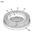
- Fig. 1 is a perspective view of a lamp device according to an embodiment of the present invention.
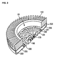
- Fig. 2 is a perspective view of a cross section of the lamp device according to the embodiment shown in Fig. 1 of the present invention.
- Fig. 3 is an exploded perspective view of a lamp device according to the embodiment shown in Fig. 1 of the present invention.
- a lamp device 100 includes a heat radiating body 110, a substrate 130, a light source unit 150, a light guider 170, a flange 190, a first member 210, a condensing lens 220, a second member 230 and a fixing member 250.
- the heat radiating body 110 is formed by organically coupling a ring structure 111, a plurality of fins 113 and a flat portion 115, so that the heat radiating body 110 has a shape of a donut.
- the shape of the heat radiating body 110 is not limited to this.
- the heat radiating body 110 may have a polygonal shape or other various shapes.
- the ring structure 111 has an inner surface and an outer surface such that an opening G1 having a central axis "A" is formed in the center of the ring structure 111.
- a plurality of the fins 113 are joined to the outer surface of the ring structure 111 and radially extend to the outside from the outer surface of the ring structure 111.
- a plurality of the fins 113 may be separated from each other at a regular interval such that heat generated from a light source unit 150 which will be described below is wholly uniformly radiated to the outside.
- the flat portion 115 is joined to one end of the outer surface of the ring structure 111 and extends perpendicular to the outer surface of the ring structure 111.
- the flat portion 115 is joined to one ends of a plurality of the fins 113 joined to the outer surface of the ring structure 111.
- the substrate 130 includes a top surface and a bottom surface.
- the top surface comes in surface contact with the flat portion 115 of the heat radiating body.
- the light source unit 150 is disposed on the bottom surface. It is desirable that a commonly used metal printed circuit board (PCB) is mainly used as the substrate 130. However, any substrate capable of including the light source unit can be used as the substrate 130.
- PCB metal printed circuit board
- the substrate 130 has a disk shape for sealing the ring structure 111 having the opening G1.
- the substrate 130 is required to have an opening G2 in the center thereof in order that heat generated from the light source unit 150 can be radiated to the outside through the circulation of the air.
- the opening G2 at the center of the substrate is placed corresponding to the opening G1 of the heat radiating body such that they have the same central axis "A".
- the light source unit 150 includes a plurality of light emitting diodes (LEDs).
- LEDs light emitting diodes
- a plurality of the LEDs are radially disposed on the bottom surface of the substrate. That is, a plurality of the LEDs may be disposed on the bottom surface of the substrate 130 at a regular interval just like a plurality of the fins 113 are disposed.
- the radiation area of heat generated from the operation of the LEDs becomes greater, so that heat release efficiency is improved.
- the heat from the LEDs is radiated through the surface contact between the flat portion of the heat radiating body and the top surface of the substrate and through a plurality of the fins of the heat radiating body, As a result, heat radiating surface area is increased so that a heat transfer characteristic is improved.
- a conductive sheet for radiating heat is further added between the substrate 130 and the flat portion 115 of the heat radiating body 110, so that it is possible to enhance the heat transfer characteristic between the substrate 130 and the heat radiating body 110.
- the light guider 170 includes a plurality of optical fibers. One end of each optical fiber is optically connected to a plurality of the LEDs 150.
- the optical fiber is taken as an example of the light guider 170, any device like a prism of an optical device capable of changing the direction of light generated by the light source unit into a desired direction can be used as the light guider 170.
- the flange 190 includes a plurality of holes 191 for inserting and binding the ends of a plurality of the optical fibers, and has an entire shape of a disk. Therefore, a plurality of the LEDs are bound by the flange 190, so that a wide emission area of light generated from a plurality of the radially disposed LEDs becomes smaller. As a result, the light is collected in a particular direction.
- the ends of the optical fibers inserted into the holes 191 of the flange 190 are aligned with the holes 191 of the flange such that the ends are placed on the same plane. This intends to obtain the uniform intensity of light at a particular plane on which the light is incident.
- the flange is seated in an opening G3 of the first member 210 which will be described below, so that the flange has an optical orientation plane according to the adjustment of the angle of the first member 210.
- the first member 210 includes a first projection 212, a second projection 213 and a first ring structure 211 having an inner surface and an outer surface such that a circular opening G3 having a central axis is formed in the center of the first ring structure 211.
- the first projection 212 and the second projection 213 are formed on the outer surface of the first ring structure 211 to face each other.
- the first projection 212 and the second projection 213 extend from the outer surface of the first ring structure 211 to the outside.
- the first projection 212 and the second projection 213 of the first member 210 are inserted into a first hole 231a and a second hole 231b of the second member 230, which are described below, respectively. Accordingly, the first member 210 is joined and fixed to the second member 230.
- the first member 210 is inclined at an angle to rotate about the first projection 212 and the second projection 213. Therefore, light generated from the light source unit 150 can be directed to a direction that a user desires by through adjustment of the angle of the first member 210.
- the condensing lens 220 is optically joined to the first member 210 and covers the opening opposite to the first member's circular opening in which the flange 190 is seated. Such a condensing lens more optically condenses the light which has been physically condensed by the flange.
- the second member 230 includes a first projection 232, a second projection 233 and a second ring structure 231 having an inner surface and an outer surface such that a circular opening G4 having a central axis is formed in the center of the second ring structure 231.
- the second member 230 includes the first hole 231a and the second hole 231b into which the first and the second projections 212 and 213 of the first member 210 are inserted.
- the first hole 231a and the second hole 231b penetrate the inner and outer surfaces of the second ring structure 231 and face each other.
- the first and the second projections 232 and 233 extend from the outer surface of the second ring structure 231 to the outside.
- a first imaginary line horizontally extending from the first projection 232 to the second projection 233 is at a right angle to a second imaginary line extending from the central axis of the first hole 231a to the central axis of the second hole 231b.
- the circumferential extent of the inner surface of the second member 230 is greater than that of the outer surface of the first member 210, so that the first member 210 is inserted into the second member 230.
- the fixing member 250 includes an inner circumferential portion 251 such that a circular opening G5 having a central axis of the inner circumferential portion 251 is formed, an outer circumferential portion 253 formed along the inner circumferential portion at a regular interval from the inner circumferential portion 251, and flat portion 255 extending vertically from the end of the inner circumferential portion to the end of the outer circumferential portion.
- the inner circumferential portion 251 of the fixing member 250 includes mutually facing first and second holes 251a and 251b into which the first projection 232 and the second projection 233 are inserted.
- the first projection 232 and the second projection 233 of the second member 230 are respectively inserted into the first hole 251a and the second hole 251b of the fixing member 250.
- the second member 230 is joined and fixed to inner surface of the inner circumferential portion 251 of the fixing member 250.
- the outer circumferential portion 253 of the fixing member 250 surrounds the light source unit 150 and the light guider 170.
- the lamp device mentioned above includes a heat radiating body having a structure in which the heat generated from the light emitting diodes can be radiated spatially not in an up-and-down direction but in a horizontal direction when the lamp device is operated, the entire volume of the lamp device can be actually reduced. Accordingly, as compared with a conventional heat radiating body radiating heat in the up-and-down direction, the heat radiating body of the present invention has a lower spatial limitation when the lamp device is installed. As a result, installation flexibility can be improved.
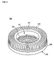
- Fig. 4 is a perspective view of another lamp device according to an embodiment of the present invention.
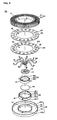
- Fig. 5 is an exploded perspective view of the lamp device according to the embodiment shown in Fig. 4 of the present invention.
- another lamp device 300 includes a heat radiating body 310, a heat radiating plate 330, a substrate 350, a light source unit 370, a light guider 390, a flange 410, a first member 430, a second member 450 and a fixing member 470.
- the heat radiating body 310 is formed by organically coupling a ring structure 311 and a plurality of fins 313, so that the heat radiating body 310 has a shape of a donut.
- the shape of the heat radiating body 310 is not limited to this.
- the structure 311 may have a polygonal shape or other various shapes.
- the ring structure 311 has an inner surface and an outer surface such that an opening G1' having a central axis "A" is formed in the center of the ring structure 311.
- a plurality of the fins 313 which are joined to the outer surface of the ring structure 311 and radially extend to the outside from the outer surface of the ring structure 311.
- a plurality of the fins 313 are separated from each other at a regular interval such that heat generated from a light source unit 370 which will be described below is wholly uniformly radiated to the outside. That is, two adjacent fins may be spaced apart from each other at a regular interval.
- the heat radiating plate 330 includes a hole 331 located at an area corresponding to the interval between the two adjacent fins among a plurality of the fins 313, and contacts with a plurality of the radially disposed fins 313.
- the heat radiating plate 330 also includes a central opening G2' placed corresponding to the central opening G1' of the heat radiating body 310.
- the hole 331 of the heat radiating plate 330 has a rectangular shape which is actually parallel with the longitudinal direction of the fin such that the external air more easily flows in from the top of the heat radiating body. When the substrate directly contacts with a plurality of the fins of the heat radiating body, the heat radiating plate 330 may be omitted.
- the heat radiating plate 330 is integrally formed with the heat radiating body 310, the heat radiating body 110 shown in Fig. 3 can be actually formed. In other words, the heat radiating plate 330 is able to function as the flat portion 115 of the heat radiating body 110 shown in Fig. 3 .
- the substrate 350 includes a top surface and a bottom surface.
- the top surface comes in surface contact with the heat radiating plate 330.
- the light source unit 370 is disposed on the bottom surface. It is desirable that a commonly used metal printed circuit board (PCB) is mainly used as the substrate 350. However, any substrate capable of including the light source unit can be used as the substrate 350.
- PCB metal printed circuit board
- the substrate 350 has a disk shape for sealing the heat radiating plate 330 having the opening G2'.
- the substrate 350 is required to have an opening G3' in the center thereof in order that heat generated from the light source unit 370 can be radiated to the outside through the circulation of the external air.
- the opening G3' at the center of the substrate 350 is placed corresponding to the opening G2' of the heat radiating plate 330.
- the substrate 350 includes a plurality of holes 351. A plurality of the holes 351 are placed between the light source units 370 which will be disposed on the bottom surface of the substrate.
- the holes of the substrate are disposed between the light source units 370 and correspond to the holes 331 of the heat radiating plate 330.
- the hole 351 of the substrate has also a rectangular shape.
- the substrate 350 is able to directly contact with a plurality of the fins of the heat radiating body and transfer heat without the heat radiating plate. It is possible to improve the heat transfer characteristic between the heat radiating body and the heat radiating plate or between the heat radiating plate and the substrate by adding a conductive sheet between the heat radiating body and the heat radiating plate or between the heat radiating plate and the substrate.
- the light source unit 370 includes a plurality of light emitting diodes (LEDs).
- a plurality of the LEDs are radially disposed on the bottom surface of the substrate. That is, a plurality of the LEDs are disposed on the bottom surface of the substrate 350 just like a plurality of the fins 313 of the heat radiating body 310 are disposed.
- the radiation area of heat generated from the operation of the LEDs becomes greater, so that heat release efficiency is improved.
- the heat from the LEDs can be radiated by the circulation of the air through the holes of either the substrate or the heat radiating plate.
- a plurality of the fins of the heat radiating body increase the heat radiation surface area, so that a heat transfer characteristic is improved.
- a conductive sheet for radiating heat is further added between the substrate and the heat radiating plate, so that it is possible to enhance the heat transfer characteristic between the substrate and the heat radiating plate.
- the light guider 390, the flange 410, the first member 430, a condensing lens 440, the second member 450 and the fixing member 470 are similar to those of the one embodiment of the present invention, the descriptions thereof will be omitted.
Description
- This embodiment relates to a lamp device.
- A light emitting diode (LED) is an energy device converting electric energy into light energy and has low power consumption, a semi-permanent life span, a rapid response speed, safeness and environment-friendliness as compared with existing light sources like a fluorescent light, an incandescent lamp and the like.
- Therefore, many researches are devoted to substitution of the existing light sources with the LED. The LED is now increasingly used as a light source for lighting devices, for example, a liquid crystal display device, an electric sign, a street lamp, a pilot lamp, a room lamp and the like.
-
- In this embodiment, it is possible to effectively radiate heat generated by operating a lamp device.
- In this embodiment, when there are problems in the parts of the lamp device, it is possible to easily repair and maintain the problems.
- In this embodiment, it is possible to improve the installation flexibility without a spatial limitation by reducing the volume of the lamp device.
- One embodiment is a lamp device includes: a heat radiating body (310) comprising a structure (311) and a plurality of fins (313), wherein the structure (311) comprises an inner surface and an outer surface such that an opening G1' is formed and wherein a plurality of the fins (313) extend to the outside from the outer surface of the structure (311); and a substrate (350) being under a plurality of the fins (313) of the heat radiating body (310) and comprising a plurality of light emitting devices (370) disposed on one side thereof, characterized in that the lamp device further comprises a plurality of optical fibers (390) of which one ends are optically connected to a plurality of the light emitting devices (370) respectively.
-
-
Fig. 1 is a perspective view of a lamp device according to an embodiment of the present invention. -
Fig. 2 is a perspective view of a cross section of the lamp device according to the embodiment shown inFig. 1 of the present invention. -
Fig. 3 is an exploded perspective view of a lamp device according to the embodiment shown inFig. 1 of the present invention. -
Fig. 4 is a perspective view of another lamp device according to an embodiment of the present invention. -
Fig. 5 is an exploded perspective view of the lamp device according to the embodiment shown inFig. 4 of the present invention. - A thickness or size of each layer is magnified, omitted or schematically shown for the purpose of convenience and clearness of description. The size of each component does not necessarily mean its actual size.
- It will be understood that when an element is referred to as being 'on' or "under" another element, it can be directly on/under the element, and one or more intervening elements may also be present. When an element is referred to as being 'on' or 'under', 'under the element' as well as 'on the element' can be included based on the element.
- Hereinafter, an embodiment will be described with reference to the accompanying drawings.
-
Fig. 1 is a perspective view of a lamp device according to an embodiment of the present invention.Fig. 2 is a perspective view of a cross section of the lamp device according to the embodiment shown inFig. 1 of the present invention.Fig. 3 is an exploded perspective view of a lamp device according to the embodiment shown inFig. 1 of the present invention. - Referring to
Figs. 1 to 3 , alamp device 100 according to an embodiment of the present invention includes aheat radiating body 110, asubstrate 130, alight source unit 150, alight guider 170, aflange 190, afirst member 210, acondensing lens 220, asecond member 230 and afixing member 250. - The
heat radiating body 110 is formed by organically coupling aring structure 111, a plurality offins 113 and aflat portion 115, so that theheat radiating body 110 has a shape of a donut. However, the shape of theheat radiating body 110 is not limited to this. For example, theheat radiating body 110 may have a polygonal shape or other various shapes. - The
ring structure 111 has an inner surface and an outer surface such that an opening G1 having a central axis "A" is formed in the center of thering structure 111. A plurality of thefins 113 are joined to the outer surface of thering structure 111 and radially extend to the outside from the outer surface of thering structure 111. A plurality of thefins 113 may be separated from each other at a regular interval such that heat generated from alight source unit 150 which will be described below is wholly uniformly radiated to the outside. Theflat portion 115 is joined to one end of the outer surface of thering structure 111 and extends perpendicular to the outer surface of thering structure 111. Theflat portion 115 is joined to one ends of a plurality of thefins 113 joined to the outer surface of thering structure 111. - The
substrate 130 includes a top surface and a bottom surface. The top surface comes in surface contact with theflat portion 115 of the heat radiating body. Thelight source unit 150 is disposed on the bottom surface. It is desirable that a commonly used metal printed circuit board (PCB) is mainly used as thesubstrate 130. However, any substrate capable of including the light source unit can be used as thesubstrate 130. - The
substrate 130 has a disk shape for sealing thering structure 111 having the opening G1. In addition, thesubstrate 130 is required to have an opening G2 in the center thereof in order that heat generated from thelight source unit 150 can be radiated to the outside through the circulation of the air. The opening G2 at the center of the substrate is placed corresponding to the opening G1 of the heat radiating body such that they have the same central axis "A". Here, it is required that the opening G2 at the center of the substrate and the opening G1 of the heat radiating body have the same area for the purpose of improving the assemblability and heat radiating characteristic of the lamp device. - The
light source unit 150 includes a plurality of light emitting diodes (LEDs). A plurality of the LEDs are radially disposed on the bottom surface of the substrate. That is, a plurality of the LEDs may be disposed on the bottom surface of thesubstrate 130 at a regular interval just like a plurality of thefins 113 are disposed. - As such, when a plurality of the LEDs are radially disposed on the substrate, the radiation area of heat generated from the operation of the LEDs becomes greater, so that heat release efficiency is improved. The heat from the LEDs is radiated through the surface contact between the flat portion of the heat radiating body and the top surface of the substrate and through a plurality of the fins of the heat radiating body, As a result, heat radiating surface area is increased so that a heat transfer characteristic is improved.
- Though not shown in the drawings, a conductive sheet for radiating heat is further added between the
substrate 130 and theflat portion 115 of theheat radiating body 110, so that it is possible to enhance the heat transfer characteristic between thesubstrate 130 and theheat radiating body 110. - Since a plurality of the LEDs are mounted and disposed on one substrate instead of separate substrates, if necessary, it is possible to easily repair and maintain the substrate including the light source unit.
- The
light guider 170 includes a plurality of optical fibers. One end of each optical fiber is optically connected to a plurality of theLEDs 150. In the present embodiment, though the optical fiber is taken as an example of thelight guider 170, any device like a prism of an optical device capable of changing the direction of light generated by the light source unit into a desired direction can be used as thelight guider 170. - The
flange 190 includes a plurality ofholes 191 for inserting and binding the ends of a plurality of the optical fibers, and has an entire shape of a disk. Therefore, a plurality of the LEDs are bound by theflange 190, so that a wide emission area of light generated from a plurality of the radially disposed LEDs becomes smaller. As a result, the light is collected in a particular direction. - The ends of the optical fibers inserted into the
holes 191 of theflange 190 are aligned with theholes 191 of the flange such that the ends are placed on the same plane. This intends to obtain the uniform intensity of light at a particular plane on which the light is incident. The flange is seated in an opening G3 of thefirst member 210 which will be described below, so that the flange has an optical orientation plane according to the adjustment of the angle of thefirst member 210. - The
first member 210 includes afirst projection 212, asecond projection 213 and afirst ring structure 211 having an inner surface and an outer surface such that a circular opening G3 having a central axis is formed in the center of thefirst ring structure 211. Thefirst projection 212 and thesecond projection 213 are formed on the outer surface of thefirst ring structure 211 to face each other. Thefirst projection 212 and thesecond projection 213 extend from the outer surface of thefirst ring structure 211 to the outside. Thefirst projection 212 and thesecond projection 213 of thefirst member 210 are inserted into afirst hole 231a and asecond hole 231b of thesecond member 230, which are described below, respectively. Accordingly, thefirst member 210 is joined and fixed to thesecond member 230. - The
first member 210 is inclined at an angle to rotate about thefirst projection 212 and thesecond projection 213. Therefore, light generated from thelight source unit 150 can be directed to a direction that a user desires by through adjustment of the angle of thefirst member 210. - The condensing
lens 220 is optically joined to thefirst member 210 and covers the opening opposite to the first member's circular opening in which theflange 190 is seated. Such a condensing lens more optically condenses the light which has been physically condensed by the flange. - Like the
first member 210, thesecond member 230 includes afirst projection 232, asecond projection 233 and asecond ring structure 231 having an inner surface and an outer surface such that a circular opening G4 having a central axis is formed in the center of thesecond ring structure 231. Thesecond member 230 includes thefirst hole 231a and thesecond hole 231b into which the first and thesecond projections first member 210 are inserted. Thefirst hole 231a and thesecond hole 231b penetrate the inner and outer surfaces of thesecond ring structure 231 and face each other. The first and thesecond projections second ring structure 231 to the outside. - In such a
second member 230, a first imaginary line horizontally extending from thefirst projection 232 to thesecond projection 233 is at a right angle to a second imaginary line extending from the central axis of thefirst hole 231a to the central axis of thesecond hole 231b. - The circumferential extent of the inner surface of the
second member 230 is greater than that of the outer surface of thefirst member 210, so that thefirst member 210 is inserted into thesecond member 230. - The fixing
member 250 includes an innercircumferential portion 251 such that a circular opening G5 having a central axis of the innercircumferential portion 251 is formed, an outercircumferential portion 253 formed along the inner circumferential portion at a regular interval from the innercircumferential portion 251, andflat portion 255 extending vertically from the end of the inner circumferential portion to the end of the outer circumferential portion. - The inner
circumferential portion 251 of the fixingmember 250 includes mutually facing first andsecond holes first projection 232 and thesecond projection 233 are inserted. Thefirst projection 232 and thesecond projection 233 of thesecond member 230 are respectively inserted into thefirst hole 251a and thesecond hole 251b of the fixingmember 250. Thesecond member 230 is joined and fixed to inner surface of the innercircumferential portion 251 of the fixingmember 250. - The outer
circumferential portion 253 of the fixingmember 250 surrounds thelight source unit 150 and thelight guider 170. - Since the lamp device mentioned above includes a heat radiating body having a structure in which the heat generated from the light emitting diodes can be radiated spatially not in an up-and-down direction but in a horizontal direction when the lamp device is operated, the entire volume of the lamp device can be actually reduced. Accordingly, as compared with a conventional heat radiating body radiating heat in the up-and-down direction, the heat radiating body of the present invention has a lower spatial limitation when the lamp device is installed. As a result, installation flexibility can be improved.
-
Fig. 4 is a perspective view of another lamp device according to an embodiment of the present invention.Fig. 5 is an exploded perspective view of the lamp device according to the embodiment shown inFig. 4 of the present invention. - Referring to
Figs. 4 to 5 , anotherlamp device 300 according to one embodiment of the present invention includes aheat radiating body 310, aheat radiating plate 330, asubstrate 350, alight source unit 370, alight guider 390, aflange 410, afirst member 430, asecond member 450 and a fixingmember 470. - The
heat radiating body 310 is formed by organically coupling aring structure 311 and a plurality offins 313, so that theheat radiating body 310 has a shape of a donut. However, the shape of theheat radiating body 310 is not limited to this. For example, thestructure 311 may have a polygonal shape or other various shapes. Thering structure 311 has an inner surface and an outer surface such that an opening G1' having a central axis "A" is formed in the center of thering structure 311. A plurality of thefins 313 which are joined to the outer surface of thering structure 311 and radially extend to the outside from the outer surface of thering structure 311. A plurality of thefins 313 are separated from each other at a regular interval such that heat generated from alight source unit 370 which will be described below is wholly uniformly radiated to the outside. That is, two adjacent fins may be spaced apart from each other at a regular interval. - The
heat radiating plate 330 includes ahole 331 located at an area corresponding to the interval between the two adjacent fins among a plurality of thefins 313, and contacts with a plurality of the radially disposedfins 313. Theheat radiating plate 330 also includes a central opening G2' placed corresponding to the central opening G1' of theheat radiating body 310. Thehole 331 of theheat radiating plate 330 has a rectangular shape which is actually parallel with the longitudinal direction of the fin such that the external air more easily flows in from the top of the heat radiating body. When the substrate directly contacts with a plurality of the fins of the heat radiating body, theheat radiating plate 330 may be omitted. If theheat radiating plate 330 is integrally formed with theheat radiating body 310, theheat radiating body 110 shown inFig. 3 can be actually formed. In other words, theheat radiating plate 330 is able to function as theflat portion 115 of theheat radiating body 110 shown inFig. 3 . - The
substrate 350 includes a top surface and a bottom surface. The top surface comes in surface contact with theheat radiating plate 330. Thelight source unit 370 is disposed on the bottom surface. It is desirable that a commonly used metal printed circuit board (PCB) is mainly used as thesubstrate 350. However, any substrate capable of including the light source unit can be used as thesubstrate 350. - The
substrate 350 has a disk shape for sealing theheat radiating plate 330 having the opening G2'. In addition, thesubstrate 350 is required to have an opening G3' in the center thereof in order that heat generated from thelight source unit 370 can be radiated to the outside through the circulation of the external air. Here, the opening G3' at the center of thesubstrate 350 is placed corresponding to the opening G2' of theheat radiating plate 330. Additionally, thesubstrate 350 includes a plurality ofholes 351. A plurality of theholes 351 are placed between thelight source units 370 which will be disposed on the bottom surface of the substrate. - It is more desirable that the holes of the substrate are disposed between the
light source units 370 and correspond to theholes 331 of theheat radiating plate 330. Like thehole 331 of theheat radiating plate 330, thehole 351 of the substrate has also a rectangular shape. - Though not shown in the drawings, the
substrate 350 is able to directly contact with a plurality of the fins of the heat radiating body and transfer heat without the heat radiating plate. It is possible to improve the heat transfer characteristic between the heat radiating body and the heat radiating plate or between the heat radiating plate and the substrate by adding a conductive sheet between the heat radiating body and the heat radiating plate or between the heat radiating plate and the substrate. - The
light source unit 370 includes a plurality of light emitting diodes (LEDs). A plurality of the LEDs are radially disposed on the bottom surface of the substrate. That is, a plurality of the LEDs are disposed on the bottom surface of thesubstrate 350 just like a plurality of thefins 313 of theheat radiating body 310 are disposed. - As such, when a plurality of the LEDs are radially disposed on the substrate, the radiation area of heat generated from the operation of the LEDs becomes greater, so that heat release efficiency is improved. The heat from the LEDs can be radiated by the circulation of the air through the holes of either the substrate or the heat radiating plate. A plurality of the fins of the heat radiating body increase the heat radiation surface area, so that a heat transfer characteristic is improved. Though not shown in the drawings, a conductive sheet for radiating heat is further added between the substrate and the heat radiating plate, so that it is possible to enhance the heat transfer characteristic between the substrate and the heat radiating plate.
- Since a plurality of the LEDs are mounted and disposed on one substrate instead of separate substrates, if necessary, it is possible to easily repair and maintain the substrate including the light source unit.
- Since the
light guider 390, theflange 410, thefirst member 430, a condensinglens 440, thesecond member 450 and the fixingmember 470 are similar to those of the one embodiment of the present invention, the descriptions thereof will be omitted. - The features, structures and effects and the like described in the embodiments are included in at least one embodiment of the present invention and are not necessarily limited to one embodiment. Furthermore, the features, structures and effects and the like provided in each embodiment can be combined or modified in other embodiments by those skilled in the art to which the embodiments belong. Therefore, the contents related to the combination and modification should be construed to be included in the scope of the present invention.
- The foregoing embodiments and advantages are merely exemplary and are not to be construed as limiting the present invention. The present teaching can be readily applied to other types of apparatuses. The description of the foregoing embodiments is intended to be illustrative, and not to limit the scope of the claims. Many alternatives, modifications, and variations will be apparent to those skilled in the art. In the claims, means-plus-function clauses are intended to cover the structures described herein as performing the recited function and not only structural equivalents but also equivalent structures.
Claims (15)
- A lamp device comprising:a heat radiating body (310) comprising a structure (311) and a plurality of fins (313), wherein the structure (311) comprises an inner surface and an outer surface such that an opening (G1') is formed and wherein a plurality of the fins (313) extend to the outside from the outer surface of the structure (311) ; anda substrate (350) being under a plurality of the fins (313) of the heat radiating body (310) and comprising the plurality of light emitting devices (370) disposed on one side thereof,characterized in that the lamp device further comprises a plurality of optical fibers (390) of which one end is optically connected to respectively one light emitting device of the plurality of light emitting devices (370).
- The lamp device of claim 1, wherein the substrate (350) comprises an opening (G3') formed such that the opening (G3') corresponds to the opening (G1') of the heat radiating body (310).
- The lamp device of claim 2, wherein the opening G1' of the heat radiating body (310) and the opening G3' of the substrate (350) have the same central axis.
- The lamp device of claim 1, wherein the structure (311) has a ring shape.
- The lamp device of claim 1, further comprising a heat radiating plate (330) being located between the substrate (350) and the plurality of the fins (313) of the heat radiating body (310), and having an opening (G2') corresponding to the opening of the heat radiating body (310), wherein the heat radiating plate (330) comes in surface contact with the substrate (350).
- The lamp device of claim 5, wherein two adjacent fins among the plurality of the fins (313) of the heat radiating body (310) are spaced apart from each other at a predetermined interval, wherein the heat radiating plate (330) comprises a hole (331) located at an area corresponding to the interval between the two fins (313), and wherein one side of the heat radiating plate (330) contacts with the plurality of the fins (313).
- The lamp device of claim 1, wherein the other ends of the plurality of the optical fibers (390) are bound to each other.
- The lamp device of claim 1, wherein the plurality of the fins (313) of the heat radiating body (310) are separated from each other at a regular interval.
- The lamp device of claim 1 or claim 5, wherein the plurality of the fins (313) of the heat radiating body (310) directly contact with one side of the substrate (350).
- The lamp device of claim 1, wherein the plurality of the light emitting devices (370) are radially disposed on one side of the substrate (350).
- The lamp device of claim 1 or claim 10, wherein the plurality of the light emitting devices (370) are disposed at a regular interval on the one side of the substrate (350).
- The lamp device of claim 1, further comprising a flange (410) having a plurality of holes (411) for inserting and binding the ends of the plurality of the optical fibers (390).
- The lamp device of claim 12, further comprising a first member (430) including a first ring structure (431) having an inner surface and an outer surface such that a circular opening (G4') is formed and projections (432, 433) extending from the first ring structure (431),
wherein the flange (410) is seated in the opening (G4') of the first member (430), and wherein the first ring structure (431) is rotated about the projections (432, 433). - The lamp device of claim 13, further comprising a second member (450) including a second ring structure (451), projections (452, 453) and holes (451a, 451b),
wherein the second ring structure (451) has an inner surface and an outer surface such that a circular opening (G5') is formed,
wherein the projections (452, 453) extend from the second ring structure (451), and
wherein the holes (451a, 451b) are inserted into the projections (432, 433) of the first member (430). - The lamp device of claim 14, wherein a first imaginary line horizontally extending from the projections (452, 453) of the second member (450) is at a right angle to a second imaginary line extending from the holes (451a, 451b).
Applications Claiming Priority (2)
| Application Number | Priority Date | Filing Date | Title |
|---|---|---|---|
| KR1020100091547A KR101742678B1 (en) | 2010-09-17 | 2010-09-17 | Lamp apparatus |
| EP11153747A EP2431660B1 (en) | 2010-09-17 | 2011-02-08 | Lamp device |
Related Parent Applications (1)
| Application Number | Title | Priority Date | Filing Date |
|---|---|---|---|
| EP11153747A Division EP2431660B1 (en) | 2010-09-17 | 2011-02-08 | Lamp device |
Publications (2)
| Publication Number | Publication Date |
|---|---|
| EP2511606A1 EP2511606A1 (en) | 2012-10-17 |
| EP2511606B1 true EP2511606B1 (en) | 2014-01-15 |
Family
ID=43929048
Family Applications (2)
| Application Number | Title | Priority Date | Filing Date |
|---|---|---|---|
| EP11153747A Active EP2431660B1 (en) | 2010-09-17 | 2011-02-08 | Lamp device |
| EP12176009.4A Active EP2511606B1 (en) | 2010-09-17 | 2011-02-08 | Lamp device |
Family Applications Before (1)
| Application Number | Title | Priority Date | Filing Date |
|---|---|---|---|
| EP11153747A Active EP2431660B1 (en) | 2010-09-17 | 2011-02-08 | Lamp device |
Country Status (5)
| Country | Link |
|---|---|
| US (1) | US8476813B2 (en) |
| EP (2) | EP2431660B1 (en) |
| JP (2) | JP5868622B2 (en) |
| KR (1) | KR101742678B1 (en) |
| CN (1) | CN102410515B (en) |
Families Citing this family (6)
| Publication number | Priority date | Publication date | Assignee | Title |
|---|---|---|---|---|
| USD671257S1 (en) * | 2010-04-10 | 2012-11-20 | Lg Innotek Co., Ltd. | LED lamp |
| US8297790B2 (en) * | 2010-08-18 | 2012-10-30 | Lg Innotek Co., Ltd. | Lamp device |
| KR101742678B1 (en) | 2010-09-17 | 2017-06-01 | 엘지이노텍 주식회사 | Lamp apparatus |
| CN102606950B (en) * | 2012-03-02 | 2013-11-27 | 中山伟强科技有限公司 | LED projection lamp |
| CN103411186A (en) * | 2013-08-10 | 2013-11-27 | 无锡市宝成塑胶科技有限公司 | Thermally-conductive resin lamp holder for LED panel lamps |
| KR102116272B1 (en) | 2017-04-21 | 2020-05-29 | 주식회사 케이엠더블유 | Multiple input multiple output antenna apparatus |
Family Cites Families (23)
| Publication number | Priority date | Publication date | Assignee | Title |
|---|---|---|---|---|
| JPH11202164A (en) * | 1998-01-19 | 1999-07-30 | Toyoda Gosei Co Ltd | Optical source module |
| JP3066834U (en) * | 1999-08-23 | 2000-03-07 | 株式会社遠藤照明 | Recessed ceiling light with replaceable lighting unit |
| US6371628B1 (en) * | 2000-02-03 | 2002-04-16 | Lucifer Lighting Company | Post-installation adjustable lighting fixture |
| JP2002367406A (en) * | 2001-06-05 | 2002-12-20 | Algol:Kk | Ring-like led lighting system |
| US6832849B2 (en) | 2001-12-04 | 2004-12-21 | Ccs, Inc. | Light radiation device, light source device, light radiation unit, and light connection mechanism |
| JP3966845B2 (en) * | 2003-09-29 | 2007-08-29 | 株式会社松村電機製作所 | LED lighting device |
| US7329887B2 (en) * | 2003-12-02 | 2008-02-12 | 3M Innovative Properties Company | Solid state light device |
| WO2005057669A2 (en) * | 2003-12-02 | 2005-06-23 | 3M Innovative Properties Company | Irradiation apparatus |
| US7258474B2 (en) | 2005-04-21 | 2007-08-21 | Magna International Inc. | Headlamp with beam patterns formed from semiconductor light sources |
| JP4492458B2 (en) * | 2005-06-22 | 2010-06-30 | パナソニック電工株式会社 | lighting equipment |
| US7431475B2 (en) | 2005-07-22 | 2008-10-07 | Sony Corporation | Radiator for light emitting unit, and backlight device |
| US7588359B2 (en) * | 2005-09-26 | 2009-09-15 | Osram Sylvania Inc. | LED lamp with direct optical coupling in axial arrangement |
| US8789962B2 (en) * | 2005-10-27 | 2014-07-29 | Vikon Surgical, Llc | Surgical headlight |
| US7663229B2 (en) * | 2006-07-12 | 2010-02-16 | Hong Kong Applied Science And Technology Research Institute Co., Ltd. | Lighting device |
| CN201028412Y (en) * | 2006-12-29 | 2008-02-27 | 梁立人 | Head rotating lamp |
| WO2009044716A1 (en) * | 2007-10-01 | 2009-04-09 | Koha Co., Ltd. | Light emitting device |
| US7458706B1 (en) * | 2007-11-28 | 2008-12-02 | Fu Zhun Precision Industry (Shen Zhen) Co., Ltd. | LED lamp with a heat sink |
| JP2009140718A (en) * | 2007-12-05 | 2009-06-25 | Toshiba Lighting & Technology Corp | Lighting apparatus |
| US7682049B2 (en) * | 2008-04-15 | 2010-03-23 | Fu Zhun Precision Industry (Shen Zhen) Co., Ltd. | LED lamp |
| JP2010108792A (en) * | 2008-10-30 | 2010-05-13 | Toshiba Lighting & Technology Corp | Luminaire |
| IT1392500B1 (en) * | 2008-12-30 | 2012-03-09 | I B T S P A | LED DISSIPATION OPTIMIZED HEAT LIGHTING DEVICE FOR OUTDOOR AND LARGE COVERED AREAS |
| DE102009008096B4 (en) * | 2009-02-09 | 2016-10-27 | Osram Gmbh | Heat sink for a lighting device |
| KR101742678B1 (en) | 2010-09-17 | 2017-06-01 | 엘지이노텍 주식회사 | Lamp apparatus |
-
2010
- 2010-09-17 KR KR1020100091547A patent/KR101742678B1/en active IP Right Grant
-
2011
- 2011-02-08 EP EP11153747A patent/EP2431660B1/en active Active
- 2011-02-08 EP EP12176009.4A patent/EP2511606B1/en active Active
- 2011-03-04 US US13/040,779 patent/US8476813B2/en active Active
- 2011-03-22 CN CN201110072437.2A patent/CN102410515B/en active Active
- 2011-07-08 JP JP2011151734A patent/JP5868622B2/en active Active
-
2016
- 2016-01-06 JP JP2016001095A patent/JP6196330B2/en active Active
Also Published As
| Publication number | Publication date |
|---|---|
| CN102410515A (en) | 2012-04-11 |
| US20110204764A1 (en) | 2011-08-25 |
| KR101742678B1 (en) | 2017-06-01 |
| JP6196330B2 (en) | 2017-09-13 |
| EP2431660B1 (en) | 2012-11-07 |
| JP2012064562A (en) | 2012-03-29 |
| JP2016042492A (en) | 2016-03-31 |
| JP5868622B2 (en) | 2016-02-24 |
| KR20120029632A (en) | 2012-03-27 |
| US8476813B2 (en) | 2013-07-02 |
| EP2511606A1 (en) | 2012-10-17 |
| EP2431660A1 (en) | 2012-03-21 |
| CN102410515B (en) | 2014-06-11 |
Similar Documents
| Publication | Publication Date | Title |
|---|---|---|
| EP2420720B1 (en) | Lamp device | |
| US8083375B2 (en) | Lamp device | |
| EP2511606B1 (en) | Lamp device | |
| JP5284522B1 (en) | Optical semiconductor lighting device | |
| US10571084B2 (en) | Lighting module, and lighting apparatus having same | |
| CN101614367B (en) | Light-emitting diode lamp | |
| JP2014072194A (en) | Heat radiation module and combination type lighting device having the same | |
| KR101055053B1 (en) | Lighting device | |
| KR101929256B1 (en) | Lighting device | |
| KR101733465B1 (en) | The radiant heat structure for a LED lamp | |
| KR101742679B1 (en) | Lamp apparatus | |
| JP2013020734A (en) | Outdoor lighting fixture | |
| KR101761384B1 (en) | Lamp apparatus | |
| KR101752421B1 (en) | Lamp apparatus | |
| KR101860039B1 (en) | Lighting device | |
| KR20140103459A (en) | Lighting apparatus | |
| KR20110005131U (en) | LED lamp improved assembly and maintenance properties | |
| KR20170124381A (en) | LED lighting device | |
| KR20170043041A (en) | Led lighting apparatus | |
| KR20110011330A (en) | Lighting device |
Legal Events
| Date | Code | Title | Description |
|---|---|---|---|
| PUAI | Public reference made under article 153(3) epc to a published international application that has entered the european phase |
Free format text: ORIGINAL CODE: 0009012 |
|
| AC | Divisional application: reference to earlier application |
Ref document number: 2431660 Country of ref document: EP Kind code of ref document: P |
|
| AK | Designated contracting states |
Kind code of ref document: A1 Designated state(s): AL AT BE BG CH CY CZ DE DK EE ES FI FR GB GR HR HU IE IS IT LI LT LU LV MC MK MT NL NO PL PT RO RS SE SI SK SM TR |
|
| RIN1 | Information on inventor provided before grant (corrected) |
Inventor name: KONG, KYUNG-IL |
|
| 17P | Request for examination filed |
Effective date: 20130412 |
|
| GRAP | Despatch of communication of intention to grant a patent |
Free format text: ORIGINAL CODE: EPIDOSNIGR1 |
|
| INTG | Intention to grant announced |
Effective date: 20130523 |
|
| GRAS | Grant fee paid |
Free format text: ORIGINAL CODE: EPIDOSNIGR3 |
|
| GRAP | Despatch of communication of intention to grant a patent |
Free format text: ORIGINAL CODE: EPIDOSNIGR1 |
|
| INTG | Intention to grant announced |
Effective date: 20131007 |
|
| GRAA | (expected) grant |
Free format text: ORIGINAL CODE: 0009210 |
|
| AC | Divisional application: reference to earlier application |
Ref document number: 2431660 Country of ref document: EP Kind code of ref document: P |
|
| AK | Designated contracting states |
Kind code of ref document: B1 Designated state(s): AL AT BE BG CH CY CZ DE DK EE ES FI FR GB GR HR HU IE IS IT LI LT LU LV MC MK MT NL NO PL PT RO RS SE SI SK SM TR |
|
| REG | Reference to a national code |
Ref country code: CH Ref legal event code: EP Ref country code: GB Ref legal event code: FG4D |
|
| REG | Reference to a national code |
Ref country code: AT Ref legal event code: REF Ref document number: 650008 Country of ref document: AT Kind code of ref document: T Effective date: 20140215 |
|
| REG | Reference to a national code |
Ref country code: IE Ref legal event code: FG4D |
|
| REG | Reference to a national code |
Ref country code: DE Ref legal event code: R096 Ref document number: 602011004745 Country of ref document: DE Effective date: 20140227 |
|
| REG | Reference to a national code |
Ref country code: NL Ref legal event code: T3 |
|
| REG | Reference to a national code |
Ref country code: AT Ref legal event code: MK05 Ref document number: 650008 Country of ref document: AT Kind code of ref document: T Effective date: 20140115 |
|
| REG | Reference to a national code |
Ref country code: LT Ref legal event code: MG4D |
|
| PG25 | Lapsed in a contracting state [announced via postgrant information from national office to epo] |
Ref country code: IS Free format text: LAPSE BECAUSE OF FAILURE TO SUBMIT A TRANSLATION OF THE DESCRIPTION OR TO PAY THE FEE WITHIN THE PRESCRIBED TIME-LIMIT Effective date: 20140515 Ref country code: NO Free format text: LAPSE BECAUSE OF FAILURE TO SUBMIT A TRANSLATION OF THE DESCRIPTION OR TO PAY THE FEE WITHIN THE PRESCRIBED TIME-LIMIT Effective date: 20140415 Ref country code: LT Free format text: LAPSE BECAUSE OF FAILURE TO SUBMIT A TRANSLATION OF THE DESCRIPTION OR TO PAY THE FEE WITHIN THE PRESCRIBED TIME-LIMIT Effective date: 20140115 |
|
| PG25 | Lapsed in a contracting state [announced via postgrant information from national office to epo] |
Ref country code: SE Free format text: LAPSE BECAUSE OF FAILURE TO SUBMIT A TRANSLATION OF THE DESCRIPTION OR TO PAY THE FEE WITHIN THE PRESCRIBED TIME-LIMIT Effective date: 20140115 Ref country code: ES Free format text: LAPSE BECAUSE OF FAILURE TO SUBMIT A TRANSLATION OF THE DESCRIPTION OR TO PAY THE FEE WITHIN THE PRESCRIBED TIME-LIMIT Effective date: 20140115 Ref country code: PT Free format text: LAPSE BECAUSE OF FAILURE TO SUBMIT A TRANSLATION OF THE DESCRIPTION OR TO PAY THE FEE WITHIN THE PRESCRIBED TIME-LIMIT Effective date: 20140515 Ref country code: FI Free format text: LAPSE BECAUSE OF FAILURE TO SUBMIT A TRANSLATION OF THE DESCRIPTION OR TO PAY THE FEE WITHIN THE PRESCRIBED TIME-LIMIT Effective date: 20140115 Ref country code: AT Free format text: LAPSE BECAUSE OF FAILURE TO SUBMIT A TRANSLATION OF THE DESCRIPTION OR TO PAY THE FEE WITHIN THE PRESCRIBED TIME-LIMIT Effective date: 20140115 Ref country code: CY Free format text: LAPSE BECAUSE OF FAILURE TO SUBMIT A TRANSLATION OF THE DESCRIPTION OR TO PAY THE FEE WITHIN THE PRESCRIBED TIME-LIMIT Effective date: 20140115 |
|
| PG25 | Lapsed in a contracting state [announced via postgrant information from national office to epo] |
Ref country code: RS Free format text: LAPSE BECAUSE OF FAILURE TO SUBMIT A TRANSLATION OF THE DESCRIPTION OR TO PAY THE FEE WITHIN THE PRESCRIBED TIME-LIMIT Effective date: 20140115 Ref country code: LV Free format text: LAPSE BECAUSE OF FAILURE TO SUBMIT A TRANSLATION OF THE DESCRIPTION OR TO PAY THE FEE WITHIN THE PRESCRIBED TIME-LIMIT Effective date: 20140115 Ref country code: BE Free format text: LAPSE BECAUSE OF FAILURE TO SUBMIT A TRANSLATION OF THE DESCRIPTION OR TO PAY THE FEE WITHIN THE PRESCRIBED TIME-LIMIT Effective date: 20140115 Ref country code: HR Free format text: LAPSE BECAUSE OF FAILURE TO SUBMIT A TRANSLATION OF THE DESCRIPTION OR TO PAY THE FEE WITHIN THE PRESCRIBED TIME-LIMIT Effective date: 20140115 |
|
| REG | Reference to a national code |
Ref country code: CH Ref legal event code: PL |
|
| REG | Reference to a national code |
Ref country code: DE Ref legal event code: R097 Ref document number: 602011004745 Country of ref document: DE |
|
| PG25 | Lapsed in a contracting state [announced via postgrant information from national office to epo] |
Ref country code: CZ Free format text: LAPSE BECAUSE OF FAILURE TO SUBMIT A TRANSLATION OF THE DESCRIPTION OR TO PAY THE FEE WITHIN THE PRESCRIBED TIME-LIMIT Effective date: 20140115 Ref country code: RO Free format text: LAPSE BECAUSE OF FAILURE TO SUBMIT A TRANSLATION OF THE DESCRIPTION OR TO PAY THE FEE WITHIN THE PRESCRIBED TIME-LIMIT Effective date: 20140115 Ref country code: CH Free format text: LAPSE BECAUSE OF NON-PAYMENT OF DUE FEES Effective date: 20140228 Ref country code: EE Free format text: LAPSE BECAUSE OF FAILURE TO SUBMIT A TRANSLATION OF THE DESCRIPTION OR TO PAY THE FEE WITHIN THE PRESCRIBED TIME-LIMIT Effective date: 20140115 Ref country code: LI Free format text: LAPSE BECAUSE OF NON-PAYMENT OF DUE FEES Effective date: 20140228 Ref country code: MC Free format text: LAPSE BECAUSE OF FAILURE TO SUBMIT A TRANSLATION OF THE DESCRIPTION OR TO PAY THE FEE WITHIN THE PRESCRIBED TIME-LIMIT Effective date: 20140115 Ref country code: DK Free format text: LAPSE BECAUSE OF FAILURE TO SUBMIT A TRANSLATION OF THE DESCRIPTION OR TO PAY THE FEE WITHIN THE PRESCRIBED TIME-LIMIT Effective date: 20140115 |
|
| PLBE | No opposition filed within time limit |
Free format text: ORIGINAL CODE: 0009261 |
|
| STAA | Information on the status of an ep patent application or granted ep patent |
Free format text: STATUS: NO OPPOSITION FILED WITHIN TIME LIMIT |
|
| PG25 | Lapsed in a contracting state [announced via postgrant information from national office to epo] |
Ref country code: SK Free format text: LAPSE BECAUSE OF FAILURE TO SUBMIT A TRANSLATION OF THE DESCRIPTION OR TO PAY THE FEE WITHIN THE PRESCRIBED TIME-LIMIT Effective date: 20140115 Ref country code: PL Free format text: LAPSE BECAUSE OF FAILURE TO SUBMIT A TRANSLATION OF THE DESCRIPTION OR TO PAY THE FEE WITHIN THE PRESCRIBED TIME-LIMIT Effective date: 20140115 |
|
| REG | Reference to a national code |
Ref country code: IE Ref legal event code: MM4A |
|
| 26N | No opposition filed |
Effective date: 20141016 |
|
| REG | Reference to a national code |
Ref country code: FR Ref legal event code: PLFP Year of fee payment: 5 |
|
| PG25 | Lapsed in a contracting state [announced via postgrant information from national office to epo] |
Ref country code: IE Free format text: LAPSE BECAUSE OF NON-PAYMENT OF DUE FEES Effective date: 20140208 |
|
| REG | Reference to a national code |
Ref country code: DE Ref legal event code: R097 Ref document number: 602011004745 Country of ref document: DE Effective date: 20141016 |
|
| PG25 | Lapsed in a contracting state [announced via postgrant information from national office to epo] |
Ref country code: SI Free format text: LAPSE BECAUSE OF FAILURE TO SUBMIT A TRANSLATION OF THE DESCRIPTION OR TO PAY THE FEE WITHIN THE PRESCRIBED TIME-LIMIT Effective date: 20140115 |
|
| REG | Reference to a national code |
Ref country code: FR Ref legal event code: PLFP Year of fee payment: 6 |
|
| PG25 | Lapsed in a contracting state [announced via postgrant information from national office to epo] |
Ref country code: MT Free format text: LAPSE BECAUSE OF FAILURE TO SUBMIT A TRANSLATION OF THE DESCRIPTION OR TO PAY THE FEE WITHIN THE PRESCRIBED TIME-LIMIT Effective date: 20140115 |
|
| PG25 | Lapsed in a contracting state [announced via postgrant information from national office to epo] |
Ref country code: SM Free format text: LAPSE BECAUSE OF FAILURE TO SUBMIT A TRANSLATION OF THE DESCRIPTION OR TO PAY THE FEE WITHIN THE PRESCRIBED TIME-LIMIT Effective date: 20140115 |
|
| PG25 | Lapsed in a contracting state [announced via postgrant information from national office to epo] |
Ref country code: BG Free format text: LAPSE BECAUSE OF FAILURE TO SUBMIT A TRANSLATION OF THE DESCRIPTION OR TO PAY THE FEE WITHIN THE PRESCRIBED TIME-LIMIT Effective date: 20140115 Ref country code: GR Free format text: LAPSE BECAUSE OF FAILURE TO SUBMIT A TRANSLATION OF THE DESCRIPTION OR TO PAY THE FEE WITHIN THE PRESCRIBED TIME-LIMIT Effective date: 20140416 Ref country code: IT Free format text: LAPSE BECAUSE OF FAILURE TO SUBMIT A TRANSLATION OF THE DESCRIPTION OR TO PAY THE FEE WITHIN THE PRESCRIBED TIME-LIMIT Effective date: 20140115 |
|
| PG25 | Lapsed in a contracting state [announced via postgrant information from national office to epo] |
Ref country code: HU Free format text: LAPSE BECAUSE OF FAILURE TO SUBMIT A TRANSLATION OF THE DESCRIPTION OR TO PAY THE FEE WITHIN THE PRESCRIBED TIME-LIMIT; INVALID AB INITIO Effective date: 20110208 Ref country code: TR Free format text: LAPSE BECAUSE OF FAILURE TO SUBMIT A TRANSLATION OF THE DESCRIPTION OR TO PAY THE FEE WITHIN THE PRESCRIBED TIME-LIMIT Effective date: 20140115 Ref country code: LU Free format text: LAPSE BECAUSE OF NON-PAYMENT OF DUE FEES Effective date: 20140208 |
|
| REG | Reference to a national code |
Ref country code: FR Ref legal event code: PLFP Year of fee payment: 7 |
|
| REG | Reference to a national code |
Ref country code: FR Ref legal event code: PLFP Year of fee payment: 8 |
|
| PGFP | Annual fee paid to national office [announced via postgrant information from national office to epo] |
Ref country code: NL Payment date: 20180108 Year of fee payment: 8 |
|
| PG25 | Lapsed in a contracting state [announced via postgrant information from national office to epo] |
Ref country code: MK Free format text: LAPSE BECAUSE OF FAILURE TO SUBMIT A TRANSLATION OF THE DESCRIPTION OR TO PAY THE FEE WITHIN THE PRESCRIBED TIME-LIMIT Effective date: 20140115 |
|
| PG25 | Lapsed in a contracting state [announced via postgrant information from national office to epo] |
Ref country code: AL Free format text: LAPSE BECAUSE OF FAILURE TO SUBMIT A TRANSLATION OF THE DESCRIPTION OR TO PAY THE FEE WITHIN THE PRESCRIBED TIME-LIMIT Effective date: 20140115 |
|
| REG | Reference to a national code |
Ref country code: NL Ref legal event code: MM Effective date: 20190301 |
|
| PG25 | Lapsed in a contracting state [announced via postgrant information from national office to epo] |
Ref country code: NL Free format text: LAPSE BECAUSE OF NON-PAYMENT OF DUE FEES Effective date: 20190301 |
|
| REG | Reference to a national code |
Ref country code: GB Ref legal event code: 732E Free format text: REGISTERED BETWEEN 20210722 AND 20210728 |
|
| REG | Reference to a national code |
Ref country code: DE Ref legal event code: R081 Ref document number: 602011004745 Country of ref document: DE Owner name: SUZHOU LEKIN SEMICONDUCTOR CO. LTD., TAICANG, CN Free format text: FORMER OWNER: LG INNOTEK CO., LTD., SEOUL, KR |
|
| PGFP | Annual fee paid to national office [announced via postgrant information from national office to epo] |
Ref country code: FR Payment date: 20230110 Year of fee payment: 13 |
|
| PGFP | Annual fee paid to national office [announced via postgrant information from national office to epo] |
Ref country code: GB Payment date: 20230105 Year of fee payment: 13 Ref country code: DE Payment date: 20230104 Year of fee payment: 13 |