EP2508902A1 - Testkontaktor für eine Leiterplatte, Verwendung und Verfahren zum Prüfen - Google Patents
Testkontaktor für eine Leiterplatte, Verwendung und Verfahren zum Prüfen Download PDFInfo
- Publication number
- EP2508902A1 EP2508902A1 EP12002417A EP12002417A EP2508902A1 EP 2508902 A1 EP2508902 A1 EP 2508902A1 EP 12002417 A EP12002417 A EP 12002417A EP 12002417 A EP12002417 A EP 12002417A EP 2508902 A1 EP2508902 A1 EP 2508902A1
- Authority
- EP
- European Patent Office
- Prior art keywords
- contact
- circuit board
- printed circuit
- pressure element
- test contactor
- Prior art date
- Legal status (The legal status is an assumption and is not a legal conclusion. Google has not performed a legal analysis and makes no representation as to the accuracy of the status listed.)
- Granted
Links
Images


Classifications
-
- G—PHYSICS
- G01—MEASURING; TESTING
- G01R—MEASURING ELECTRIC VARIABLES; MEASURING MAGNETIC VARIABLES
- G01R31/00—Arrangements for testing electric properties; Arrangements for locating electric faults; Arrangements for electrical testing characterised by what is being tested not provided for elsewhere
- G01R31/28—Testing of electronic circuits, e.g. by signal tracer
- G01R31/2801—Testing of printed circuits, backplanes, motherboards, hybrid circuits or carriers for multichip packages [MCP]
- G01R31/2806—Apparatus therefor, e.g. test stations, drivers, analysers, conveyors
- G01R31/2808—Holding, conveying or contacting devices, e.g. test adapters, edge connectors, extender boards
-
- H—ELECTRICITY
- H01—ELECTRIC ELEMENTS
- H01R—ELECTRICALLY-CONDUCTIVE CONNECTIONS; STRUCTURAL ASSOCIATIONS OF A PLURALITY OF MUTUALLY-INSULATED ELECTRICAL CONNECTING ELEMENTS; COUPLING DEVICES; CURRENT COLLECTORS
- H01R12/00—Structural associations of a plurality of mutually-insulated electrical connecting elements, specially adapted for printed circuits, e.g. printed circuit boards [PCB], flat or ribbon cables, or like generally planar structures, e.g. terminal strips, terminal blocks; Coupling devices specially adapted for printed circuits, flat or ribbon cables, or like generally planar structures; Terminals specially adapted for contact with, or insertion into, printed circuits, flat or ribbon cables, or like generally planar structures
- H01R12/70—Coupling devices
- H01R12/82—Coupling devices connected with low or zero insertion force
- H01R12/85—Coupling devices connected with low or zero insertion force contact pressure producing means, contacts activated after insertion of printed circuits or like structures
- H01R12/89—Coupling devices connected with low or zero insertion force contact pressure producing means, contacts activated after insertion of printed circuits or like structures acting manually by moving connector housing parts linearly, e.g. slider
-
- H—ELECTRICITY
- H01—ELECTRIC ELEMENTS
- H01R—ELECTRICALLY-CONDUCTIVE CONNECTIONS; STRUCTURAL ASSOCIATIONS OF A PLURALITY OF MUTUALLY-INSULATED ELECTRICAL CONNECTING ELEMENTS; COUPLING DEVICES; CURRENT COLLECTORS
- H01R2201/00—Connectors or connections adapted for particular applications
- H01R2201/20—Connectors or connections adapted for particular applications for testing or measuring purposes
Definitions
- the present invention relates to a test contactor for a printed circuit board, a use of the test contactor and a method for testing a printed circuit board.
- a printed circuit board is understood to be a printed circuit board (also called “PCB” or “printed circuit board”).
- a circuit board may include one or more electrical and / or electronic components, such as integrated circuits (also called “integrated circuits”), resistors, capacitors, diodes, transistors, and so forth.
- printed circuits are tested after manufacture for operability.
- Many printed circuit boards have board edge contacts so that the boards can be electrically and mechanically connected to a mother board by inserting their edge into a board connector.
- the board connector contacts In order for the electrical and mechanical connection to be permanent, the board connector contacts must apply a predetermined contact force to the board edge contacts of the inserted board causing the insertion to take place with a great deal of force necessary to force the contacts of the board connector apart , It also occurs during insertion of a friction between the contacts of the board connector and the board edge contacts of the circuit board.
- test board For testing printed circuit boards, these are pushed into a board connector of a test board, tested and then removed again. Sometimes the testing of printed circuit boards takes place automatically in testing machines, so that the individual for the test necessary operating conditions should be produced by the testing machine. Due to the frequent PCB changes and the resulting abrasion of the contacts of the board connector of the test board, the test board has a very limited life.
- test contactor it is therefore an object of the present invention to provide a test contactor, a use of the test contactor, and a method of inspecting printed circuit boards, which enables the inspection of printed circuit boards in large numbers and in a simple manner.
- This object is achieved by the test contactor according to claim 1, the use of the test contactor according to claim 9 and the method according to claim 10.
- Preferred embodiments are the subject of the dependent claims.
- Test contactor according to one aspect
- the printed circuit board can be inserted without contact into the intermediate space between the first printed circuit board contact side and the second printed circuit board contact side.
- non-contact in the sense of the application means that the at least one first contact element does not come into contact with the printed circuit board when the printed circuit board is inserted in the open position.
- the electrical and mechanical contact of the at least one contact element with the printed circuit board can be produced only by the transfer of the test contact in the operating position.
- the non-contact insertion of the printed circuit board into the test contactor causes no friction to occur between the at least one first contact element and the printed circuit board. Therefore, the printed circuit board in particular in the sense force-free inserted into the Testuttonor that no frictional resistance between the circuit board and the at least one first contact element is overcome. For example, the printed circuit board can only fall into the gap due to gravity. In other words occurs during insertion of the circuit board along the insertion direction E no friction, which must be overcome by a force.
- the distance d O is dimensioned such that the printed circuit board in the open position without contact, in particular without a frictional engagement with the first and second pressure element, along the insertion direction E is inserted.
- the distance d O may be at least about 3 mm, preferably at least about 5 mm or at least about 10 mm. In particular, the distance d O may be about 4 mm, for example 4.1 mm.
- the at least one first contact element projects preferably along the direction of displacement over the first printed circuit board contact side, in particular by about 0.1 mm to about 2 mm, more preferably by about 0.5 mm to about 1 mm. Accordingly, a distance d K in the open position between the at least one first contact element and the second circuit board contact side at least about 2.5 mm or at least about 3 mm, preferably at least about 4.5 mm or at least about 8 mm.
- the distance d K can be between about 3.3 mm and about 3.4 mm, in particular 3.36 mm. Only in the operating position are the at least one first contact element and the at least one associated first board edge contact of the printed circuit board contacted with each other and in particular in frictional engagement with each other. Since there is no abrasive stress on the at least one first contact element when the printed circuit board is inserted and decontacted, the at least one first contact is generally wear-free.
- the test contactor has the first pressure element and the second pressure element, which are displaceable relative to one another along the displacement direction V.
- both pressure elements are linearly displaceable relative to each other.
- the first and second pressure element can be designed to be displaceable or linearly displaceable or arranged.
- the first and second pressure element can move in opposite directions along the direction of displacement V to move from the open position to the operating position.
- a distinction is not made between a displacement along and against the direction of displacement V, since both pressure elements move in opposite directions.
- only the first pressure element or the second pressure element could be designed to be displaceable or displaceable, while the respective other pressure element is fixedly mounted on the test contactor.
- Between the first and second pressure element is in the open position of the test contact a gap, in which the circuit board at least partially along the insertion direction E can be inserted. Insertion direction E and displacement direction V are preferably perpendicular to each other.
- At least a first contact element is arranged on the first printed circuit board contact side of the first pressure element, which faces the intermediate space. It is understood that two first, three, four, five, ..., ten, ..., one hundred, one hundred and five, one hundred and fifteen, etc. first contact elements can be formed or arranged on the first circuit board contact side. In contrast, the second PCB contact side be free of contact elements. It is understood that in this case only printed circuit boards can be contacted completely electrically by means of the test contact, which have board edge contacts only on a corresponding printed circuit board side.
- the distance d B between the first circuit board contact side and the second circuit board contact side along the displacement direction V is smaller than the distance d o .
- the distance d B may be at least about 2 mm, preferably at least about 1.5 mm or at least about 1 mm, for example about 1.2 mm or about 1.1 mm. Due to the contacting of the at least one first contact element with the circuit board, the distance between the at least one first contact element and the second circuit board contact side is dependent on the thickness of the circuit board.
- the distance d B may be substantially equal to the printed circuit board thickness. As used herein, the term "substantially" means that the distance d B can be up to about 0.1 mm greater than the thickness of the circuit board to provide clearance in the operative position.
- the circuit board thickness is 0.8 mm to 1.6 mm, in particular, 0.8 mm, 1.0 mm, 1.55 mm and 1.6 mm. Accordingly, a distance d K in the operating position between the at least one first contact element and the second circuit board contact side can be about 0.8 mm to about 1.6 mm.
- the first and second pressure elements are displaced toward each other in order to move from the open position to the operating position.
- the at least one first contact element reaches the at least one associated first edge edge contact of the printed circuit board in an electrical and mechanical contact.
- each of the at least one first contact elements can apply a predetermined contact pressure F K on the associated board edge contact, whereby advantageously a predetermined contact resistance is reached or undershot.
- operating position thus describes a state of the test contactor in which the printed circuit board to be tested is electrically contacted in such a way that an electrical test of the function of the printed circuit board by means of the test contactor can be carried out, ie the operational use of the test contactor is possible.
- the distance d G between the first board contact side and the second board contact side along the displacement direction V in the closed position is smaller than the distance d O and may be smaller than the distance d B in the operating position. In particular, the distance d G can be zero.
- the second pressure element comprises at least one second contact element, wherein the at least one second contact element in the operating position can be contacted with at least one associated second platinum edge contact of the printed circuit board.
- the circuit board is non-contact insertable to the at least one second contact element in the intermediate space between the first circuit board contact side and the second circuit board contact side.
- the non-contact insertion of the printed circuit board into the test contact prevents friction between the at least one second contact element and the printed circuit board.
- the at least one second contact element like the at least one first contact element, is essentially free of wear, since there is no abrasive stress on the at least one second contact element when the printed circuit board is inserted or decontacted.
- the at least one first contact element of the first pressure element and the at least one second contact element of the second pressure element are preferably arranged opposite, so that the printed circuit board during insertion into the Testuttonor along the insertion direction E between the at least one first contact element and the at least one second contact element can be arranged or is arranged.
- this can be at least a first Contact element and contact the at least one second contact element in the operating position respectively associated board edge contacts of the circuit boards, wherein the at least one first board edge contact, which is assigned to the at least one first contact element, is arranged on the side of the circuit board, which is opposite to the side of the circuit board, on which the at least one second board edge contact is located, which is associated with the at least one second contact element.
- the first contact element (s) and the second contact element (s) may contact board edge contacts associated in the operative position on opposite sides of the circuit board, respectively.
- the number of second contact elements is equal to the number of first contact elements.
- the second pressing member on the second board contact side may have two, three, four, five, ..., ten, ..., one hundred, one hundred and five, one hundred and fifteen, etc. second contact members.
- a distance d K in the open position between the at least one first contact element and the at least one second contact element may be for example at least about 2 mm or at least about 2.5 mm, preferably at least about 4 mm, at least about 8 mm, in particular about 3 , 36 mm.
- the distance d K between the at least one first contact element and the at least one second contact element in the open position between about 2 mm and about 10 mm, preferably between about 3 mm and about 5 mm, so that a circuit board to be tested at least partially along the Insertion direction E between the first and second contact elements can be inserted.
- the first and second contact elements along the displacement direction V can shift so that the distance d K between the at least one first contact element and the at least one second contact element in the operating position is between about 0.5 mm and about 1.6 mm, preferably about 1 mm. It is understood that the distance d K between the first and second contact elements in the operating position is limited by the interposed circuit board through the thickness of the circuit board down. In other words, the distance d K can not be smaller than the thickness of the printed circuit board.
- the first pressure element preferably has at least one first ground contact element, which protrudes further from the first circuit board contact side along the direction of displacement V than the at least one first contact element. Further preferably, the second pressure element on at least a second ground contact element, which projects, starting from the second printed circuit board contact side along the displacement direction V further than the at least one second contact element.
- non-contact insertion of the circuit board in the presence of first and / or second ground contacts also means that the printed circuit board when inserted into the Testtitleor in the open position, the first and / or second ground contacts mechanically or electrically contacted.
- an associated first board edge ground contact of the printed circuit board to be tested can be contacted by the at least one first ground contact element before the at least one first contact element contacts the assigned first board edge contact of the circuit board.
- an associated second board edge ground contact of the printed circuit board to be tested can be contacted by the at least one second ground contact element before the at least one second contact element makes contact with the associated second board edge contact of the printed circuit board.
- the at least one first ground contact element and / or the at least one second ground contact element remain in electrical contact with the printed circuit board during a displacement of the first and second pressure element from the operating position to the open position, while the electrical contact between the printed circuit board and the at least one first contact element and / or the at least one second contact element is already separated.
- the at least one first ground contact element and / or the at least one second ground contact element by about 0.05 mm to about 2 mm, more preferably by about 0.1 mm to about 2 mm, in particular by about 0.33 mm or by about 0 5 mm, project along the direction of displacement V with respect to the at least one first contact element and / or with respect to the at least one second contact element.
- the at least one first contact element and / or the at least one second contact element are formed resiliently, wherein the at least one first contact element and / or the at least one second contact element in the operating position a predetermined contact pressure F K applies to the circuit board. More preferably, the at least one first ground contact element and / or the at least one second ground contact element are formed resiliently. Accordingly, by means of the at least one first ground contact element and / or by means of the at least one second ground contact element in the operating position, a predetermined pressure force F M can be applied to the circuit board.
- each individual contact element or ground contact element of the test contactor in the operating position due to the applied pressure force can be pressed in an electrically contacting manner to an associated board edge contact or board edge ground contact of the circuit board to the contact resistance at the formed electrical contact below a certain limit value.
- resilient within the meaning of the application comprises in particular that the first and second contact elements are elastically deformable.
- Resilient in this context means that a body is deformable by the action of an external force, wherein the deformation substantially completely recedes when the external force is no longer effective, that is, the body after the action of the external force substantially to his original shape returns.
- the at least one first contact element and / or at least one first ground contact element along the displacement direction V such resilient or elastically deformable that the corresponding contact element or ground contact element flush with the first circuit board contact side.
- the at least one second contact elements and / or the at least one second ground contact element along the displacement direction V such resilient or elastically deformable that the corresponding contact element or ground contact element flush with the second circuit board contact side.
- the first and second circuit board contact side can then mechanically contact one another in the closed position, ie the distance d G is equal to zero.
- the pressing force F K which can be applied to the printed circuit board by means of the first and / or second contact elements, is preferably about 0.05 N to about 0.5 N, more preferably about 0.1 N to about 0.3 N and in particular about 0.2 N for each of the contact elements.
- the pressing force F M which can be applied by means of the first and / or second ground contact elements on the circuit board, preferably about 0.05 N to about 0.5 N, more preferably about 0.1 N to about 0.3 N and in particular about 0.2 N for each of the ground contact elements.
- the total pressing force which can be applied to one side of the circuit board, is obtained by multiplying the pressing force F K with the number of first or second contact elements, where appropriate, plus the pressing force F M multiplied by the Number of first or second ground contact elements.
- the resulting Automatan horrkraft which can be applied by means of the first and second pressure element to the circuit board, may be in a range between about 1 N and about 500 N.
- the resilient contact elements or ground contact elements may preferably be formed in one piece, for example as a resilient, electrically conductive element having a first leg, a bending region and a second leg.
- the first leg is attached to the first or second pressure element.
- the second leg is preferably connected via the bending region with the first leg.
- the second leg is pivotable relative to the first leg by the bending region about a bending axis when a force along the displacement direction V is applied to the second leg, in particular, the bending region is elastically deformed.
- the bending region is preferably at least partially formed as a circular arc, wherein the bending region is preferably bent by about 90 degrees to about 180 degrees, more preferably about 135 degrees to about 170 degrees, in particular about 160 degrees to 170 degrees.
- the electrical contact is preferably made via the second leg, the bending region and the first leg.
- the resilient contact elements or ground contact elements may preferably be formed in several pieces, for example comprising a contact pin, which is resiliently mounted in a contact sleeve.
- the contact sleeve is preferably attached to or in the first and second pressure element such that the contact pin along the displacement direction V in the contact sleeve is movable.
- a contact spring in particular a contact spring in the interior of the contact sleeve
- the resilient mounting of the contact pin is such that a compression of the contact spring takes place by pressing the contact pin into the contact sleeve and the contact spring thereby generates a corresponding counterforce.
- the contact spring may for example be a coil spring. In the operating position, the contact spring generates the predetermined pressure force of the contact element or ground contact element to the circuit board.
- the contact pin and the contact sleeve optionally also the contact spring, are formed of an electrically conductive material, such as a metal.
- the at least one first contact element is electrically connected to a test contactor board by means of a flexible first electrical line.
- the at least one second contact element is electrically connected to the test contactor plate by means of a flexible second electrical line.
- the second electrical line is the same length as the first electrical line.
- the first electrical line is contacted with the at least one first contact element and preferably with the at least one first ground contact element of the first pressure element and in particular mechanically fixed with or on the first pressure element.
- the second electrical line is contacted with the at least one second contact element and preferably with the at least one second ground contact element of the second pressure element and in particular mechanically fixed with or on the second pressure element.
- the first or second electrical line may comprise a carrier foil on which electrical lines are formed.
- the carrier film extends in a width direction B, which is substantially perpendicular to the direction of displacement V and perpendicular to the insertion direction E.
- the carrier foil of the first electrical line is designed and arranged such that during the displacement of the first pressure element, the carrier foil of the first electrical line undergoes only a bending along a bending axis parallel to the width direction B.
- the carrier foil of the second electrical line is designed and arranged such that during the displacement of the second Pressing the carrier film of the second electrical line only a bend along a bending axis parallel to the width direction B undergoes.
- the test contactor board may include other electronic components needed to perform electrical testing of the board.
- the test contactor board may have an electrical or optical interface to an external tester.
- the interface may conform to the Q7 standard.
- a spatial separation between the test contactor and the tester allows a test of the circuit board under conditions in which the electronics of the tester would be damaged, for example at low temperatures down to -25 degrees Celsius, at elevated temperatures up to about 120 degrees Celsius or under vibration.
- the test contactor preferably comprises a first pretensioning device which mechanically pretensions the first pressure element along the displacement direction V and / or a second pretensioning device which mechanically pretensions the second pressure element along the displacement direction V.
- first and / or second biasing means by means of the first and / or second biasing means, a biasing force along the displacement direction V on the first and / or second pressure element are applied, so that the circuit board is clamped in the operating position due to this biasing force between the first and second pressure element.
- the first and / or second biasing means preferably comprises springs, for example coil springs, which are designed and arranged such that the first and / or second biasing means is biased more in the open position of the test contact than in the operating position.
- the test contactor comprises an actuating device, with which the first pressure element and / or the second pressure element is displaceable.
- the actuating device comprises at least one eccentric cam, which between the first and second pressure element is arranged and contacted with these mechanically.
- the distance between the first and second pressure element is adjustable.
- two cams are provided on the two opposite sides of the pressure elements, whereby advantageously tilting is prevented.
- the cam (s) is or are arranged on an associated axle stub, which is rotatable by means of an actuating lever.
- two stub axles and the two cams attached thereto are rotatable by means of a single operating lever.
- the stub axle can be stored for example in a low-friction plastic sleeve in the housing of the test contactor.
- At least one first securing pin is arranged or fastened to the first pressing element, which protrudes beyond the first printed circuit board contact side along the direction of displacement V and projects displaceably into an associated opposing complementary securing pin opening of the second pressure element.
- at least one second locking pin is arranged or fastened to the second pressure element, which protrudes beyond the second printed circuit board contact side along the direction of displacement V and slidably projects into an associated opposite complementary locking pin opening of the first pressure element.
- first and / or second locking pins may be provided such that only printed circuit board of standard Q7 can be inserted into the test contactor.
- One aspect of the present invention relates to a use of a test contactor according to the invention for contacting a printed circuit board, wherein in the operating position the at least one first contact element of the first pressure element is contacted with at least one associated first edge edge contact of the printed circuit board.
- first and / or second contact elements or first and / or second ground contact elements can be electrically connected via electrical lines to a test contactor circuit board and optionally to an external test device in order to carry out a test of the circuit board.
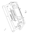
- FIG. 1 shows a perspective view of an embodiment of a test contactor 1.
- the test contactor 1 has a housing 3, in which a Porterplatteneintechnology Anlagen réelle 5 is formed.
- the printed circuit board insertion opening preferably comprises lateral insertion grooves 6 which are designed to guide the opposite sides of a printed circuit board. Therefore, the Ein Industriesnuten 6 are designed to be as wide as the thickness of the printed circuit board to be inserted, ie about 1 mm to about 2 mm.
- a printed circuit board (not shown) can be inserted at least in regions through the printed circuit board opening 5 of the housing 3 into the test contactor 1 along an insertion direction E.
- the test contactor from the open position into an operating position can be transferred.
- the in the FIG. 1 shown embodiment of the test contactor 1 is shown in a closed position, that is, that no printed circuit board is inserted into the test contactor 1 and can not be inserted in this position.
- the operating lever 7 is pressed down so that when reaching the open position at least one edge region of the circuit board (not shown) in the PCB insertion 5 of the housing 3 along the insertion direction E can be inserted.
- the Release lever 7 is released, wherein a contacting of the inserted printed circuit board with the Testtitleor 1 takes place.
- the test contactor 1 may have a suitable test electronics.
- the illustrated embodiment of the test contactor 1 comprises a test contactor board 9 which has an interface 11 with which an external tester (not shown) can be connected to the test contactor 1.
- the test of the circuit board is then carried out by means of the external tester.
- the test contactor board 9 may include other electrical or electronic components necessary to connect the circuit board to the external tester, such as components for adjusting power levels.
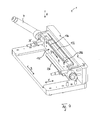
- FIG. 2 shows a section through the in FIG. 1 shown TestANDor 1 in the closed position.
- the test contactor 1 has a first pressure element 13a with a first printed circuit board contact side 15a.
- the first pressure element 13a comprises at least a first contact element 17a, in particular a multiplicity of first contact elements 17a.
- the test contactor 1 has a second pressure element 13b with a second printed circuit board contact side 15b and at least one second contact element 17b, in particular a multiplicity of second contact elements 17b.
- the first pressure element 13a and the second pressure element 13b are displaceable relative to each other along a displacement direction V, in particular linearly displaceable.
- an exemplary second contact element 17b comprises a contact pin 19b and a contact sleeve 21b, wherein the contact pin 19b is partially inserted into the contact sleeve 21b and resiliently mounted therein.
- a helical contact spring (not shown) is arranged so that the contact pin 19b further in the contact sleeve 21b is pressed, the contact spring thereby generates a corresponding counterforce.
- the force that is necessary to the contact pin 19 b by a predetermined path length in the contact sleeve 21 b is determined by the spring constant of the contact spring.
- the contact element 17b is attached via the contact sleeve 21b to the second pressure element 13b.
- the pressure element 13b may have a corresponding bore into which the contact sleeve 21b may be received at least in some areas. To attach it may be sufficient to put the contact sleeve 21 b only in a bore or blind bore, wherein the contact sleeve 21 b comes into frictional engagement with the second pressure element 13b. Further, the contact sleeve 21 b may be bonded to the second pressure element 13b or connected in some other way.
- the first contact element 17a can be formed in a corresponding manner and attached to the first pressure element 13a.
- the first contact elements 17a accommodated by the first pressure element 13a are electrically connected to the test contactor plate 9 by means of a flexible first electrical line 23a.
- each individual one of the first contact elements 17a is preferably contacted with a clearly assigned contact region of the test contactor plate 9.
- the second contact elements 17b which are received by the second pressure element 13b, are electrically connected to the test contactor plate 9 by means of a flexible second electrical line 23b.
- each of the second contact elements 17b is preferably contacted with a clearly assigned contact region of the test contactor plate 9.
- the first electrical line 23a and the second electrical line 23b are the same length.
- phase delays of signals can advantageously be avoided, which at the same time abut against a first contact element 17a and a second contact element 17b and are transmitted to the test contactor board 9 via the corresponding first electrical line 23a and second electrical line 23b, so that these signals are in phase from the test contactor board 9 be received.
- the first electrical lead 23a may comprise a carrier foil which is provided by coating with electrical conductors.
- a carrier film may have substantially the same width as the first pressure element 13a to which the first electrical line 23a is connected.
- the carrier film of The first electrical lead 23a is arranged such that the carrier foil extends in a width direction B, which is substantially perpendicular to the direction of displacement V and perpendicular to the insertion direction E.
- the carrier foil of the first electrical line 23a is bent only along a bending axis parallel to the width direction B.
- the second electrical line 23b is formed and arranged accordingly.
- the test contactor 1 comprises a first biasing device 25a, which mechanically biases the first pressure element 13a against a first abutment 27a of the test contactor 1 along the displacement direction V. Accordingly, the second pressure element 13b is mechanically biased by a second biasing device 25b relative to a second abutment 27b along the displacement direction V.
- the first and second biasing means 25a, 25b preferably comprise coil springs which are arranged between the first pressure element 13a and the first abutment 27a or between the second pressure element 13b and the second abutment 27b. The mechanical bias by means of the first and second biasing means 25a, 25b causes the test contactor 1 without external influence in the in FIG. 2 closed position shown remains.
- the distance between the first pressure element 13a and the second pressure element 13b is preferably selected such that the first contact elements 17a contact neither the opposing second contact elements 17b nor the opposite second circuit board contact side 15b. Accordingly, the second contact elements 17b in the closed position preferably do not contact the opposite first circuit board contact side 15a. Nevertheless, the distance between the first circuit board contact side 15a and the second circuit board contact side 15b may be predetermined so that a circuit board 19 in the closed position can not be inserted between the first pressure element 13a and the second pressure element 13b. In addition, the clear distance between the first PCB contact side 15a and the second PCB contact side 15b at the level of the first contact elements 17a less than 1 mm.
- the distance between the first pressure element 13a and the second pressure element 13b in the closed position may preferably be equal to zero.
- the first contact elements 17a and the second contact elements 17b are then elastically deformed.
- the individual contact pins of the contact elements can be inserted into the associated contact sleeve.
- the first pressure element 13a can be provided with at least one first securing pin 31a projecting beyond the first printed circuit board contact side 15a along the direction of displacement V, in the opposite second one Pressure element 13b is formed a complementary locking pin opening (not shown), in which the first locking pin 31 a can protrude.
- the first locking pin 31 a distance d O between the first printed circuit board contact side 15a and the second circuit board contact side 15b straddles both in the closed position, the operating position and the open position.
- the first locking pin 31 a is disposed in the region of the PCB insertion opening 5, so that the first contact elements 17 a seen from the first locking pin 31 a in the direction of the insertion direction E are arranged. Accordingly, a second locking pin (not shown) may be provided which is attached to the second circuit board contact side 15b and protrudes therefrom along the displacement direction V to project into a complementary locking pin opening of the opposing first pressing element 13a. Accordingly, 2, 3, 4 or more first and / or second locking pins may be provided.
- the at least one first securing pin 31 a can be rigidly attached to the first pressure element 13 a and accordingly, the at least one second securing pin can be rigidly attached to the second pressure element 13 b.
- At least one first locking pin 31 a can be inserted into a notch of the circuit board 29 opposite to the insertion direction E, so that the circuit board 29 along the insertion direction E in the Testuttonor 1 is inserted until the first locking pin 31 a against the edge of the notch in the printed circuit board 29 abuts, and then the first contact elements 17a can contact the associated first board edge contacts 33a of the printed circuit boards 29 when the test contactor is transferred to the operating position after insertion of the printed circuit board 29.
- FIG. 3 shows a section through an exemplary actuator of the test contact 1.
- the exemplary actuator comprises two eccentric cams 35 which are arranged in the width direction on opposite sides between each of the first pressure element 13a and the second pressure element 13b.
- the FIG. 3 shows an eccentric cam 35 on one side of the test contactor 1.
- the eccentric cam 35 may be mounted by means of a stub axle (not shown) in the housing 3 of the test contact 1, for example by means of a ball bearing or a low-friction plastic sleeve.
- the cam 35 is rotatably supported, wherein the eccentric cam 35 is rotatable by operating the operating lever 7.
- the actuating lever 7 is preferably mechanically connected to the outside of the housing 3 with the stub axle or cam 35.
- the diameter of the Cam 35 can be increased by operating the actuating lever 7 and the associated rotation of the cam, so that the first and second pressure element 13a, 13b in opposite directions along the displacement direction V and against the mechanical stress, which of the first and second biasing means 25a, 25b is produced opposite the first and second abutments 27a, 27b.
- the test contactor reaches the open position.
- a distance d O is formed between the first circuit board contact side 15 a and the second circuit board contact side 15 b in the region of the first contact elements 17 a along the displacement direction V, which is designed such that the circuit board 29 at least partially along the first printed circuit board contact side and the second printed circuit board contact side 15 b an insertion E is introduced without contact.
- the distance d O by a factor of 2, more preferably by a factor of 5 or in particular by a factor greater than 10 may be greater than the thickness of the circuit board to be tested.
- the distance d O may be, for example, about 3 mm, about 4 mm, about 5 mm, or about 10 mm.
- the distance d O is predetermined such that the first contact elements 17a and the second contact elements 17b are spaced from each other such that the contact is freely insertable circuit board under test.
- the distance d K of the first contact elements 17a and the second contact elements 17b in the open position is greater than the width of the insertion grooves 6 of the insertion opening 5 along the displacement direction V. More preferably, the distance d K of the first contact elements 17a and the second contact elements 17b in the open position should be greater than the width of the insertion opening 5 along the displacement direction V.
- the distance between the first contact elements 17a and the second contact elements 17b allows insertion of the printed circuit board 29, without a mechanical or electrical contact occurs between the circuit board 29 and the first contact elements 17a or the second contact elements 17b, whereby a friction between the circuit board and the first and second contact elements 17a, 17b is prevented.
- this does not occur Abrasion between the contact elements.
- the in FIG. 2 shown circuit board 29 are inserted through the PCB insertion 5 of the housing 3 at least with its edge region in the test contactor 1 along the insertion direction E.
- the circuit board 29 may be provided with a correspondingly positioned notch, so that the circuit board 29 can be inserted into the space between the first pressure element 13a and the second pressure element 13b.
- the first locking pin 31 a is not arranged centrally along the width of the first pressure element 13 a, the first locking pin 31 a can also serve as reverse polarity protection, since the circuit board 29 then only in a unique way through the PCB insertion 5 in the Testutton 1 can be introduced.
- the test contactor 1 After inserting the printed circuit board 29 into the test contactor 1, the test contactor 1 can be transferred from the open position to an operating position by releasing the actuating lever 7. After releasing the operating lever 7, the first and second pressing members 13a, 13b are displaced from each other by means of the first and second biasing means 25a, 25b along the displacement direction V. In the operating position exists between the first PCB contact side 15a and the second PCB contact side 15b in the region of the first contact elements 17a along the displacement direction V, a distance D B , which is smaller than the distance D O in the open position. As a result, the first contact elements 17a contact respectively associated first board edge contacts 33a of the printed circuit board 29.
- the second contact elements 17b contact the associated second board edge contacts 33b of the printed circuit board 29a.
- the first contact elements 17a each exert a predetermined contact pressure F K on the associated board edge contacts 33a.
- the second contact elements 17b exert a predetermined pressing force F K on the associated one Board edge contacts 33b of the circuit board 29 from.
- the clear distance between the first contact elements 17a and the second contact elements 17b in the operating position is greater than the clear distance between the two in the closed position of the test contact 1.
- the clear distance between the first contact elements 17a and the second contact elements 17b in the operating position is only depending on the thickness of the printed circuit board 29.
- each of the first contact elements 17a or the second contact elements 17b sets a pressure force F K of about 0.05 N to about 0.5 N, more preferably 0.1 N to about 0.3 N, in particular 0.2 N to the circuit board 29 at.
- the first and the second board edge contacts 33a, 33b are electrically connected to the test contact printed circuit board 9 in the operating position via the first and second contact elements 17a, 17b and the first and second electrical lines 23a, 23b.
- the board 29 can be contacted with an external tester (not shown) to perform the test of the board.
- the test contactor 1 is again transferred to the open position by actuating the actuating lever 7 in order to force-free the circuit board 29 against the insertion direction E from the test contactor 1.
- FIG. 4 shows an exploded partial view of another embodiment of a test contact 1, which in addition to the features described below has all the features that already with regard to FIGS. 1 to 3 have been described. Identical features are therefore with in the FIGS. 1 to 3 used reference numerals and to the to the FIGS. 1 to 3 appropriate description is referenced.
- FIG. 4 shows a preferred second pressure element 13b, which in addition to a plurality of second contact elements 17b also has at least one second ground contact element 37b on the second printed circuit board contact side 15b which protrudes further from the second printed circuit board contact side 15b along the displacement direction V than the second contact elements 17b.
- the first pressure element not shown, at least a first Have ground contact element, which projects starting from the first circuit board contact side along the displacement direction V further than the first contact elements.
- the clear distance between the at least one first ground contact element and the at least one second ground contact element 37b is less than the clear distance between the at least one first contact element and the at least one second contact element, respectively along the displacement direction V.
- the distance d O is predetermined in the open position so that the at least one first ground contact element 37b and the at least one second ground contact element are spaced apart such that the contact is freely insertable circuit board under test.
- a distance d M between the first ground contact element and second ground contact element 37 b in the open position is greater than the width of the Einzhounuten 6 of the insertion 5 along the displacement direction V and more preferably greater than the width of the insertion opening 5 along the displacement direction V.
- distance d M may be greater than about 2 mm, greater than about 3 mm, greater than about 5 mm, or greater than about 10 mm.
- the distance d M may be, for example, 2.7 mm.
- test contactor 1 when the test contactor 1 is moved from the open position to the operating position, electrical contacting of the at least one first ground contact element with an associated first board edge ground contact (not shown) of the circuit board to be tested or electrical contacting of the at least one second ground contact element 37b with an associated one second board edge ground contact (not shown) before the at least one second contact element 17b electrically contacts the associated first board edge contact of the circuit board.
- the test circuit board is first electrically connected to ground or to the zero potential before live first and / or second contact elements 17a, 17b of the test contactor 1 can make electrical contact with the circuit board 29, thereby avoiding damage to the circuit board by voltage peaks when contacting can be.
Landscapes
- Engineering & Computer Science (AREA)
- Computer Hardware Design (AREA)
- Microelectronics & Electronic Packaging (AREA)
- General Engineering & Computer Science (AREA)
- Physics & Mathematics (AREA)
- General Physics & Mathematics (AREA)
- Tests Of Electronic Circuits (AREA)
- Measuring Leads Or Probes (AREA)
Abstract
Description
- Die vorliegende Erfindung betrifft einen Testkontaktor für eine Leiterplatte, eine Verwendung des Testkontaktors und ein Verfahren zum Prüfen einer Leiterplatte.
- Unter einer Leiterplatte wird im Sinne dieser Anmeldung eine Leiterplatte bzw. Platine für eine gedruckte Schaltung (auch "PCB", "printed circuit board" genannt) verstanden. Eine Leiterplatte kann ein oder mehrere elektrische und/oder elektronische Bauteile, wie beispielsweise integrierte Schaltkreise (auch "IC", "integrated circuit" genannt), Widerstände, Kondensatoren, Dioden, Transistoren usw. umfassen.
- Herkömmlicherweise werden gedruckte Schaltungen nach der Herstellung auf Funktionsfähigkeit geprüft. Viele Leiterplatten von gedruckten Schaltungen weisen Platinenrandkontakte (engl.: "edgeboard contact") auf, so daß die Leiterplatten durch ein Einführen ihres Randes in einen Platinenverbinder elektrisch und mechanisch mit einer Mutterleiterplatte (auch "Motherboard") verbindbar ist. Damit die elektrische und mechanische Verbindung dauerhaft ist, müssen die Kontakte des Platinenverbinders eine vorbestimmte Kontaktkraft auf die Platinenrandkontakte der eingeführten Leiterplatte anlegen, was dazu führt, daß das Einführen mit einem hohen Kraftaufwand erfolgt, welcher notwendig ist, um die Kontakte des Platinenverbinders auseinander zu drücken. Dabei tritt ebenfalls beim Einführen eine Reibung zwischen den Kontakten des Platinenverbinders und den Platinenrandkontakten der Leiterplatte auf.
- Zur Prüfung von Leiterplatten werden diese in einen Platinenverbinder einer Prüfplatine geschoben, geprüft und anschließend wieder entfernt. Mitunter findet die Prüfung der Leiterplatten automatisiert in Prüfautomaten statt, so daß die einzelnen für die Prüfung notwendigen Betriebszustände durch den Prüfautomaten herstellbar sein sollten. Aufgrund der häufigen Leiterplattenwechsel und der dabei auftretenden Abrasion der Kontakte des Platinenverbinders der Prüfplatine besitzt die Prüfplatine eine sehr begrenzte Lebensdauer.
- Es ist daher eine Aufgabe der vorliegenden Erfindung, einen Testkontaktor, eine Verwendung des Testkontaktors sowie ein Verfahren zum Prüfen von Leiterplatten bereitzustellen, welcher bzw. welches die Prüfung von Leiterplatten in grosser Stückzahl und in einfacher Weise ermöglicht. Diese Aufgabe wird gelöst durch den Testkontaktor gemäß Anspruch 1, die Verwendung des Testkontaktors gemäß Anspruch 9 sowie das Verfahren gemäß Anspruch 10. Bevorzugte Ausführungsformen sind Gegenstand der abhängigen Ansprüche.
- Ein Aspekt der vorliegenden Erfindung betrifft einen Testkontaktor zum Kontaktieren einer Leiterplatte umfassend:
- ein erstes Andruckelement mit einer ersten Leiterplattenkontaktseite und zumindest einem ersten Kontaktelement;
- ein zweites Andruckelement mit einer zweiten Leiterplattenkontaktseite, wobei das zweite Andruckelement relativ zu dem ersten Andruckelement entlang einer Verlagerungsrichtung V verlagerbar ist,
- Vorteilhafterweise ist die Leiterplatte kontaktfrei in den Zwischenraum zwischen der ersten Leiterplattenkontaktseite und der zweiten Leiterplattenkontaktseite einführbar. Der Begriff "kontaktfrei" im Sinne der Anmeldung bedeutet, daß das zumindest eine erste Kontaktelement beim Einführen der Leiterplatte in der Offenposition nicht in Kontakt mit der Leiterplatte gelangt. Der elektrische und mechanische Kontakt des zumindest einen Kontaktelement mit der Leiterplatte ist erst durch das Überführen des Testkontaktors in die Betriebsposition herstellbar.
- Insbesondere bewirkt das kontaktfreie Einführen der Leiterplatte in den Testkontaktor, daß keine Reibung zwischen dem zumindest einen ersten Kontaktelement und der Leiterplatte auftritt. Daher ist die Leiterplatte insbesondere in dem Sinne kraftfrei in den Testkontaktor einführbar, daß kein Reibungswiderstand zwischen der Leiterplatte und dem zumindest einen ersten Kontaktelement zu überwinden ist. Beispielsweise kann die Leiterplatte lediglich aufgrund der Schwerkraft in den Zwischenraum fallen. Mit anderen Worten tritt beim Einführen der Leiterplatte entlang der Einführrichtung E keine Reibung auf, welche durch einen Kraftaufwand überwunden werden muß. Der Abstand dO ist derart bemessen, daß die Leiterplatte in der Offenposition kontaktfrei, insbesondere ohne einen Reibschluß mit dem ersten und zweiten Andruckelement, entlang der Einführrichtung E einführbar ist. Beispielsweise kann der Abstand dO zumindest etwa 3 mm, bevorzugt zumindest etwa 5 mm oder zumindest etwa 10 mm betragen. Insbesondere kann der Abstand dO etwa 4 mm, beispielsweise 4,1 mm, betragen. Das zumindest eine erste Kontaktelement ragt bevorzugt entlang der Verlagerungsrichtung über die erste Leiterplattenkontaktseite hervor, insbesondere um etwa 0,1 mm bis etwa 2 mm, weiter bevorzugt um etwa 0,5 mm bis etwa 1 mm. Dem entsprechend kann ein Abstand dK in der Offenposition zwischen dem zumindest einen ersten Kontaktelement und der zweiten Leiterplattenkontaktseite zumindest etwa 2,5 mm oder zumindest etwa 3 mm, bevorzugt zumindest etwa 4,5 mm oder zumindest etwa 8 mm betragen. Insbesondere kann der Abstand dK zwischen etwa 3,3 mm und etwa 3,4 mm betragen, insbesondere 3,36 mm. Erst in der Betriebsposition sind das zumindest eine erste Kontaktelement und der zumindest eine zugeordnete erste Platinenrandkontakt der Leiterplatte miteinander kontaktiert und insbesondere in Reibschluß miteinander. Da beim Einführen und Dekontaktieren der Leiterplatte keine abrasive Beanspruchung des zumindest einen ersten Kontaktelements erfolgt, ist der zumindest eine erste Kontakt in der Regel verschleißfrei.
- Der Testkontaktor weist das erste Andruckelement und das zweite Andruckelement auf, welche entlang der Verlagerungsrichtung V relativ zueinander verlagerbar sind. Mit anderen Worten sind beide Andruckelemente relativ zueinander linear verschiebbar. Dabei können bevorzugt das erste und zweite Andruckelement verlagerbar bzw. linear verschiebbar ausgebildet bzw. angeordnet sein. Insbesondere können sich das erste und zweite Andruckelement gegenläufig entlang der Verlagerungsrichtung V bewegen, um von der Offenposition in die Betriebsposition zu gelangen. In der Anmeldung wird nicht zwischen einer Verlagerung entlang und entgegen der Verlagerungsrichtung V unterschieden, da sich beide Andruckelemente gegenläufig bewegen. Alternativ könnte auch lediglich das erste Andruckelement oder das zweite Andruckelement verlagerbar bzw. verschiebbar ausgebildet sein, während das jeweilige andere Andruckelement ortsfest an dem Testkontaktor montiert ist. Zwischen dem ersten und zweiten Andruckelement befindet sich in der Offenposition des Testkontaktors ein Zwischenraum, in welchen die Leiterplatte zumindest bereichsweise entlang der Einführrichtung E einführbar ist. Einführrichtung E und Verlagerungsrichtung V stehen bevorzugt senkrecht zueinander.
- An der ersten Leiterplattenkontaktseite des ersten Andruckelements, welche dem Zwischenraum zugewandt ist, ist zumindest ein erstes Kontaktelement angeordnet. Es versteht sich, daß an der ersten Leiterplattenkontaktseite auch zwei, drei, vier, fünf, ..., zehn, ..., hundert, hundertfünf, hundertfünfzehn usw. erste Kontaktelemente ausgebildet bzw. angeordnet sein können. Dagegen kann die zweite Leiterplattenkontaktseite frei von Kontaktelementen sein. Es versteht sich, daß in diesem Fall lediglich Leiterplatten mittels des Testkontaktors vollständig elektrisch kontaktiert werden können, die nur auf einer entsprechenden Leiterplattenseite Platinenrandkontakte aufweisen.
- Der Abstand dB zwischen der ersten Leiterplattenkontaktseite und der zweiten Leiterplattenkontaktseite entlang der Verlagerungsrichtung V ist kleiner als der Abstand dO. Beispielsweise kann der Abstand dB zumindest etwa 2 mm, bevorzugt zumindest etwa 1,5 mm oder zumindest etwa 1 mm betragen, beispielsweise etwa 1,2 mm oder etwa 1,1 mm. Aufgrund des Kontaktierens des zumindest einen ersten Kontaktelements mit der Platine, ist der Abstand zwischen dem zumindest einen ersten Kontaktelement und der zweiten Leiterplattenkontaktseite von der Dicke der Leiterplatte abhängig. Insbesondere kann der Abstand dB im wesentlichen gleich der Leiterplattendicke sein. Der Begriff "im wesentlichen" bedeutet hier, daß der Abstand dB bis etwa 0,1 mm größer sein kann als die Dicke der Leiterplatte, um ein Spiel in der Betriebsposition vorzusehen. Typischerweise beträgt die Leiterplattendicke 0,8 mm bis 1,6 mm, insbesondere, 0,8 mm, 1,0 mm, 1,55 mm und 1,6 mm. Dem entsprechend kann ein Abstand dK in der Betriebsposition zwischen dem zumindest einen ersten Kontaktelement und der zweiten Leiterplattenkontaktseite etwa 0,8 mm bis etwa 1,6 mm betragen. Mit anderen Worten werden das erste und zweite Andruckelement aufeinander zu verlagert, um von der Offenposition zur Betriebsposition zu gelangen. Dabei gelangt das zumindest eine erste Kontaktelement mit dem zumindest einem zugeordneten ersten Platinenrandkontakt der Leiterplatte in einen elektrischen und mechanischen Kontakt. Dabei kann jedes der zumindest einen ersten Kontaktelemente eine vorbestimmte Andruckkraft FK auf der zugeordneten Platinenrandkontakt anlegen, wodurch vorteilhafterweise ein vorbestimmter Übergangswiderstand erreicht bzw. unterschritten wird. Der Begriff "Betriebsposition" beschreibt demnach einen Zustand des Testkontaktors, in welchem die zu prüfende Leiterplatte derart elektrisch kontaktiert ist, daß eine elektrische Prüfung der Funktion der Leiterplatte mittels des Testkontaktors durchführbar ist, also der betriebsgemäße Gebrauch des Testkontaktors möglich ist.
- Davon zu unterscheiden ist eine Geschlossenposition, wobei keine Leiterplatte in den Testkontaktor eingeführt ist und auch keine Leiterplatte in den Testkontaktor einführbar ist. Der Abstand dG zwischen der ersten Leiterplattenkontaktseite und der zweiten Leiterplattenkontaktseite entlang der Verlagerungsrichtung V in der Geschlossenposition ist kleiner als der Abstand dO und kann kleiner sein als der Abstand dB in der Betriebsposition. Insbesondere kann der Abstand dG null sein.
- Vorzugsweise umfaßt das zweite Andruckelement zumindest ein zweites Kontaktelement, wobei das zumindest eine zweite Kontaktelement in der Betriebsposition mit zumindest einem zugeordneten zweiten Platinenkantenkontakt der Leiterplatte kontaktierbar ist.
- In der Betriebsposition sind das zumindest eine zweite Kontaktelement und der zumindest eine zugeordnete zweite Platinenrandkontakt der Leiterplatte miteinander kontaktiert und insbesondere in Reibschluß miteinander. Vorteilhafterweise ist die Leiterplatte kontaktfrei zu dem zumindest einen zweiten Kontaktelement in den Zwischenraum zwischen der ersten Leiterplattenkontaktseite und der zweiten Leiterplattenkontaktseite einführbar. Das kontaktfreie Einführen der Leiterplatte in den Testkontaktor verhindert eine Reibung zwischen dem zumindest einen zweiten Kontaktelement und der Leiterplatte. Das zumindest eine zweite Kontaktelement ist wie das zumindest eine erste Kontaktelement im wesentlichen verschleißfrei, da sowohl beim Einführen als auch beim Dekontaktieren der Leiterplatte keine abrasive Beanspruchung des zumindest einen zweiten Kontaktelements erfolgt.
- Das zumindest eine erste Kontaktelement des ersten Andruckelements und das zumindest eine zweite Kontaktelement des zweiten Andruckelements sind bevorzugt gegenüberliegend angeordnet, so daß die Leiterplatte beim Einführen in den Testkontaktor entlang der Einführrichtung E zwischen dem zumindest einen ersten Kontaktelement und dem zumindest einen zweiten Kontaktelement anordenbar bzw. angeordnet ist. Mit anderen Worten können das zumindest eine erste Kontaktelement und das zumindest eine zweite Kontaktelement in der Betriebsposition jeweils zugeordnete Platinenrandkontakte der Leiterplatten kontaktieren, wobei der zumindest eine erste Platinenrandkontakt, welcher dem zumindest einen ersten Kontaktelement zugeordnet ist, auf der Seite der Leiterplatte angeordnet ist, welche der Seite der Leiterplatte gegenüberliegt, auf welcher sich der zumindest eine zweite Platinenrandkontakt befindet, welcher dem zumindest einen zweiten Kontaktelement zugeordnet ist. Mit anderen Worten können das(die) erste(n) Kontaktelement(e) und das(die) zweite(n) Kontaktelement(e) in der Betriebsposition zugeordnete Platinenrandkontakte auf gegenüberliegenden bzw. entgegengesetzten Seiten der Leiterplatte kontaktieren.
- Bevorzugt ist die Anzahl der zweiten Kontaktelemente gleich der Anzahl der ersten Kontaktelemente. Entsprechend kann das zweite Andruckelement an der zweiten Leiterplattenkontaktseite zwei, drei, vier, fünf, ..., zehn, ..., hundert, hundertfünf, hundertfünfzehn usw. zweite Kontaktelemente aufweisen.
- Um zwischen der Offenposition und der Betriebsposition zu wechseln sind die ersten und zweiten Kontaktelemente entlang der Verlagerungsrichtung V verlagerbar, insbesondere linear verschiebbar. Das zumindest eine zweite Kontaktelement ragt bevorzugt entlang der Verlagerungsrichtung über die erste Leiterplattenkontaktseite hervor, insbesondere um etwa 0,1 mm bis etwa 2 mm, weiter bevorzugt um etwa 0,5 mm bis etwa 1 mm. Dem entsprechend kann ein Abstand dK in der Offenposition zwischen dem zumindest einen ersten Kontaktelement und dem zumindest einen zweiten Kontaktelement beispielsweise zumindest etwa 2 mm oder zumindest etwa 2,5 mm, bevorzugt zumindest etwa 4 mm, zumindest etwa 8 mm betragen, insbesondere etwa 3,36 mm. Vorzugsweise beträgt der Abstand dK zwischen dem zumindest einen ersten Kontaktelement und dem zumindest einen zweiten Kontaktelement in der Offenposition zwischen etwa 2 mm und etwa 10 mm, bevorzugt zwischen etwa 3 mm und etwa 5 mm, so daß eine zu prüfende Leiterplatte zumindest bereichsweise entlang der Einführrichtung E zwischen die ersten und zweiten Kontaktelemente einführbar ist. Weiter bevorzugt lassen sich die ersten und zweiten Kontaktelemente entlang der Verlagerungsrichtung V derart verlagern, daß der Abstand dK zwischen dem zumindest einen ersten Kontaktelement und dem zumindest einen zweiten Kontaktelement in der Betriebsposition zwischen etwa 0,5 mm und etwa 1,6 mm, bevorzugt etwa 1 mm beträgt. Es versteht sich, daß der Abstand dK zwischen den ersten und zweiten Kontaktelementen in der Betriebsposition durch die dazwischen angeordnete Leiterplatte durch die Dicke der Leiterplatte nach unten begrenzt ist. Mit anderen Worten kann der Abstand dK nicht kleiner als die Dicke der Leiterplatte sein.
- Vorzugsweise weist das erste Andruckelement zumindest ein erstes Massekontaktelement auf, welches ausgehend von der ersten Leiterplattenkontaktseite entlang der Verlagerungsrichtung V weiter vorragt als das zumindest eine erste Kontaktelement. Weiter vorzugsweise weist das zweite Andruckelement zumindest ein zweites Massekontaktelement auf, welches ausgehend von der zweiten Leiterplattenkontaktseite entlang der Verlagerungsrichtung V weiter vorragt als das zumindest eine zweite Kontaktelement. Der Begriff des "kontaktfreien Einführens der Leiterplatte" bedeutet bei Vorhandensein von ersten und/oder zweiten Massekontakten auch, daß die Leiterplatte beim Einführen in den Testkontaktor in der Offenposition die ersten und/oder zweiten Massekontakte nicht mechanisch bzw. elektrisch kontaktiert.
- Vorteilhafterweise ist ein zugeordneter erster Platinenrandmassekontakt der zu prüfenden Leiterplatte durch das zumindest eine erste Massekontaktelement kontaktierbar bevor das zumindest eine erste Kontaktelement den zugeordneten ersten Platinenrandkontakt der Leiterplatte kontaktiert. Entsprechend ist ein zugeordneter zweiter Platinenrandmassekontakt der zu prüfenden Leiterplatte durch das zumindest eine zweite Massekontaktelement kontaktierbar bevor das zumindest eine zweite Kontaktelement den zugeordneten zweiten Platinenrandkontakt der Leiterplatte kontaktiert. Dadurch ist die zu prüfende Leiterplatte bei dem Übergang des Testkontaktor von der Offenposition in die Betriebsposition mit Masse bzw. mit dem Nullpotential elektrisch verbindbar bevor spannungsführende bzw. stromführende erste und/oder zweite Kontaktelemente des Testkontaktors mit der Leiterplatte in elektrischem Kontakt treten. Vorteilhafterweise kann eine Beschädigung der Leiterplatte durch Spannungsspitzen während der Prüfung vermieden werden. Entsprechend verbleiben das zumindest eine erste Massekontaktelement und/oder das zumindest eine zweite Massekontaktelement bei einer Verlagerung des ersten und zweiten Andruckelements von der Betriebsposition in die Offenposition noch mit der Leiterplatte in elektrischem Kontakt, während der elektrische Kontakt zwischen der Leiterplatte und dem zumindest einen ersten Kontaktelement und/oder dem zumindest einen zweiten Kontaktelement bereits getrennt ist.
- Bevorzugt können das zumindest eine erste Massekontaktelement und/oder das zumindest eine zweite Massekontaktelement um etwa 0,05 mm bis etwa 2 mm, weiter bevorzugt um etwa 0,1 mm bis etwa 2 mm, insbesondere um etwa 0,33 mm oder um etwa 0,5 mm, entlang der Verlagerungsrichtung V gegenüber dem zumindest einen ersten Kontaktelement und/oder gegenüber dem zumindest einen zweiten Kontaktelement vorragen.
- Vorzugsweise sind das zumindest eine erste Kontaktelement und/oder das zumindest eine zweite Kontaktelement rückstellfähig ausgebildet, wobei das zumindest eine erste Kontaktelement und/oder das zumindest eine zweite Kontaktelement in der Betriebsposition eine vorbestimmte Andruckkraft FK auf die Leiterplatte anlegt. Weiter bevorzugt sind das zumindest eine erste Massekontaktelement und/oder das zumindest eine zweite Massekontaktelement rückstellfähig ausgebildet. Entsprechend ist mittels des zumindest einen ersten Massekontaktelements und/oder mittels des zumindest einen zweiten Massekontaktelements in der Betriebsposition eine vorbestimmte Andruckkraft FM auf die Leiterplatte anlegbar.
- Vorteilhafterweise kann jedes einzelne Kontaktelement bzw. Massekontaktelement des Testkontaktors in der Betriebsposition aufgrund der angelegten Andruckkraft derart an einen zugeordneten Platinenrandkontakt bzw. Platinenrandmassekontakt der Leiterplatte in elektrisch kontaktierender Weise gepreßt sein, um den Übergangswiderstand an dem ausgebildeten elektrischen Kontakt unterhalb eines bestimmten Grenzwertes zu halten.
- Der Begriff "rückstellfähig" im Sinne der Anmeldung umfaßt insbesondere, daß die ersten und zweiten Kontaktelemente elastisch verformbar ausgebildet sind. Rückstellfähig bedeutet in diesem Zusammenhang, daß ein Körper durch Einwirkung einer äußeren Kraft verformbar ist, wobei sich die Verformung im wesentlichen vollständig zurückbildet, wenn die äußere Kraft nicht mehr wirkt, das heißt, daß der Körper nach dem Wirken der äußeren Kraft im wesentlichen zu seiner ursprünglichen Gestalt zurückkehrt.
- Bevorzugt sind das zumindest eine erste Kontaktelement und/oder zumindest eine erste Massekontaktelement entlang der Verlagerungsrichtung V derart rückstellfähig bzw. elastisch verformbar, daß das entsprechende Kontaktelement bzw. Massekontaktelement mit der ersten Leiterplattenkontaktseite bündig bzw. eben abschließt. Weiter bevorzugt sind das zumindest eine zweite Kontaktelemente und/oder das zumindest eine zweite Massekontaktelement entlang der Verlagerungsrichtung V derart rückstellfähig bzw. elastisch verformbar, daß das entsprechende Kontaktelement bzw. Massekontaktelement mit der zweiten Leiterplattenkontaktseite bündig bzw. eben abschließt. Vorteilhafterweise können die erste und zweite Leiterplattenkontaktseite dann in der Geschlossenposition einander mechanisch kontaktieren, d.h. daß der Abstand dG gleich null ist.
- Die Andruckkraft FK, welche mittels der ersten und/oder zweiten Kontaktelemente auf die Leiterplatte anlegbar ist, beträgt vorzugsweise etwa 0,05 N bis etwa 0,5 N, weiter bevorzugt etwa 0,1 N bis etwa 0,3 N und insbesondere etwa 0,2 N für jedes der Kontaktelemente. Entsprechend beträgt die Andruckkraft FM, welche mittels der ersten und/oder zweiten Massekontaktelemente auf die Leiterplatte anlegbar ist, vorzugsweise etwa 0,05 N bis etwa 0,5 N, weiter bevorzugt etwa 0,1 N bis etwa 0,3 N und insbesondere etwa 0,2 N für jedes der Massekontaktelemente. Die gesamte Andruckkraft, welche an eine Seite der Leiterplatte anlegbar ist, ergibt sich durch Multiplikation der Andruckkraft FK mit der Anzahl der ersten oder zweiten Kontaktelemente gegebenenfalls zuzüglich der Andruckkraft FM multipliziert mit der Anzahl der ersten oder zweiten Massekontaktelemente. Die resultierende Gesamtandruckkraft, die mittels des ersten bzw. zweiten Andruckelements an die Leiterplatte anlegbar ist, kann in einem Bereich zwischen etwa 1 N und etwa 500 N liegen.
- Die rückstellfähigen Kontaktelemente bzw. Massekontaktelemente können bevorzugt einstückig ausgebildet sein, beispielsweise als federelastisches, elektrisch leitfähiges Element mit einem ersten Schenkel, einem Biegebereich und mit einem zweiten Schenkel. Der erste Schenkel ist an dem ersten oder zweiten Andruckelement befestigt. Der zweite Schenkel wird vorzugsweise über den Biegebereich mit dem ersten Schenkel verbunden. Dabei ist der zweite Schenkel gegenüber dem ersten Schenkel durch den Biegebereich um eine Biegeachse verschwenkbar, wenn eine Kraft entlang der Verlagerungsrichtung V auf den zweiten Schenkel angelegt wird, wobei insbesondere der Biegebereich elastisch verformt ist. Der Biegebereich ist vorzugsweise zumindest teilweise als Kreisbogen ausgebildet, wobei der Biegebereich bevorzugt um etwa 90 Grad bis etwa 180 Grad, besonders bevorzugt etwa 135 Grad bis etwa 170 Grad, insbesondere etwa 160 Grad bis 170 Grad, gebogen ist. Der elektrische Kontakt ist bevorzugt über den zweiten Schenkel, den Biegebereich und den ersten Schenkel hergestellt.
- Die rückstellfähigen Kontaktelemente bzw. Massekontaktelemente können bevorzugt mehrstückig ausgebildet sein, beispielsweise umfassend einen Kontaktstift, welcher in einer Kontakthülse federnd gelagert ist. Die Kontakthülse ist bevorzugt derart an bzw. in dem ersten bzw. zweiten Andruckelement befestigt, daß der Kontaktstift entlang der Verlagerungsrichtung V in der Kontakthülse beweglich ist. Mittels einer Kontaktfeder, insbesondere einer Kontaktfeder im Inneren der Kontakthülse, erfolgt die federnde Lagerung des Kontaktstiftes derart, daß durch ein Eindrücken des Kontaktstiftes in die Kontakthülse eine Kompression der Kontaktfeder erfolgt und die Kontaktfeder dadurch eine entsprechende Gegenkraft erzeugt. Die Kontaktfeder kann beispielsweise eine Spiralfeder sein. In der Betriebsposition erzeugt die Kontaktfeder die vorbestimmte Andruckkraft des Kontaktelements bzw. Massekontaktelements an die Leiterplatte. Der Kontaktstift und die Kontakthülse, gegebenenfalls auch die Kontaktfeder, sind aus einem elektrisch leitfähigen Material ausgebildet, beispielsweise einem Metall.
- Vorzugsweise ist das zumindest eine erste Kontaktelement mittels einer flexiblen ersten elektrischen Leitung mit einer Testkontaktorleiterplatte elektrisch verbunden. Weiter vorzugsweise ist das zumindest eine zweite Kontaktelement mittels einer flexiblen zweiten elektrischen Leitung mit der Testkontaktorleiterplatte elektrisch verbunden. Besonders bevorzugt ist die zweite elektrische Leitung gleich lang zu der ersten elektrischen Leitung.
- Vorteilhafterweise können durch die Verwendung einer ersten und zweiten elektrischen Leitung gleicher Länge unterschiedliche Phasenverzögerungen von Signalen zwischen der Leiterplatte und der Testkontaktorleiterplatte vermieden werden, die über unterschiedliche elektrische Leitungen übertragen werden.
- Die erste elektrische Leitung ist mit dem zumindest einen ersten Kontaktelement und bevorzugt mit dem zumindest einen ersten Massekontaktelement des ersten Andruckelements kontaktiert und insbesondere mit bzw. an dem ersten Andruckelement mechanisch fixiert. Die zweite elektrische Leitung ist mit dem zumindest einen zweiten Kontaktelement und bevorzugt mit dem zumindest einen zweiten Massekontaktelement des zweiten Andruckelements kontaktiert und insbesondere mit bzw. an dem zweiten Andruckelement mechanisch fixiert.
- Beispielsweise kann die erste bzw. zweite elektrische Leitung eine Trägerfolie umfassen, auf welcher elektrische Leitungen ausgebildet sind. Bevorzugt erstreckt sich die Trägerfolie in einer Breitenrichtung B, welche im wesentlichen senkrecht zur Verlagerungsrichtung V und senkrecht zur Einführrichtung E steht. Weiter bevorzugt ist die Trägerfolie der ersten elektrischen Leitung derart ausgebildet und angeordnet, daß bei der Verlagerung des ersten Andruckelements die Trägerfolie der ersten elektrischen Leitung lediglich eine Biegung entlang einer Biegeachse parallel zur Breitenrichtung B erfährt. Entsprechend ist die Trägerfolie der zweiten elektrischen Leitung derart ausgebildet und angeordnet, daß bei der Verlagerung des zweiten Andruckelements die Trägerfolie der zweiten elektrischen Leitung lediglich eine Biegung entlang einer Biegeachse parallel zur Breitenrichtung B erfährt.
- Die Testkontaktorleiterplatte kann weitere elektronische Bauteile aufweisen, welche benötigt werden, um eine elektrische Prüfung der Leiterplatte durchzuführen. Insbesondere kann die Testkontaktorleiterplatte eine elektrische oder optische Schnittstelle zu einem externen Prüfgerät aufweisen. Beispielsweise kann die Schnittstelle der Norm Q7 entsprechen. Vorteilhafterweise ermöglicht eine räumliche Trennung zwischen des Testkontaktors und des Prüfgeräts eine Prüfung der Leiterplatte unter Bedingungen, bei denen die Elektronik des Prüfgerätes Schaden nehmen würde, beispielsweise bei niedrigen Temperaturen bis -25 Grad Celsius, bei erhöhten Temperaturen bis etwa 120 Grad Celsius oder unter Vibrationen.
- Vorzugsweise umfaßt der Testkontaktor eine erste Vorspanneinrichtung, welche das erste Andruckelement entlang der Verlagerungrichtung V mechanisch vorspannt und/oder eine zweite Vorspanneinrichtung, welche das zweite Andruckelement entlang der Verlagerungrichtung V mechanisch vorspannt.
- Vorteilhafterweise kann mittels der ersten und/oder zweiten Vorspanneinrichtung eine Vorspannkraft entlang der Verlagerungsrichtung V auf das erste und/oder zweite Andruckelement angelegt werden, so daß die Leiterplatte in der Betriebsposition aufgrund dieser Vorspannkraft zwischen dem ersten und zweiten Andruckelement festgeklemmt ist. Die erste und/oder zweite Vorspanneinrichtung umfaßt/umfassen bevorzugt Federn, beispielsweise Spiralfedern, welche derart ausgebildet und angeordnet sind, daß die erste und/oder zweite Vorspanneinrichtung in der Offenposition des Testkontaktors stärker vorgespannt ist als in der Betriebsposition.
- Vorzugsweise umfaßt der Testkontaktor eine Betätigungseinrichtung, mit welcher das erste Andruckelement und/oder das zweite Andruckelement verlagerbar ist. Insbesondere umfaßt die Betätigungseinrichtung zumindest eine exzentrische Kurvenscheibe, welche zwischen dem ersten und zweiten Andruckelement angeordnet ist und mit diesen mechanisch kontaktiert. Durch ein Drehen der Kurvenscheibe ist der Abstand zwischen dem ersten und zweiten Andruckelement einstellbar. Besonders bevorzugt sind zwischen dem ersten und dem zweiten Andruckelement zwei Kurvenscheiben an den beiden entgegengesetzten Seiten der Andruckelemente vorgesehen, wodurch vorteilhafterweise ein Verkanten verhindert wird. Die Kurvenscheibe(n) ist bzw. sind an einem zugeordneten Achsstummel angeordnet, welcher mittels eines Betätigungshebels drehbar ist. Vorzugsweise sind mittels eines einzigen Betätigunghebels zwei Achsstummel und die daran befestigten beiden Kurvenscheiben drehbar. Die Achsstummel können beispielsweise in einer reibungsarmen Kunststoffhülse im Gehäuse des Testkontaktors gelagert sein.
- Bevorzugt ist zumindest ein erster Sicherungsstift an dem ersten Andruckelement angeordnet bzw. befestigt, welcher über die erste Leiterplattenkontaktseite entlang der Verlagerungsrichtung V vorragt und in eine zugeordnete gegenüberliegende komplementäre Sicherungsstiftöffnung des zweiten Andruckelements verschiebbar hineinragt. Weiter bevorzugt ist zumindest ein zweiter Sicherungsstift an dem zweiten Andruckelement angeordnet bzw. befestigt, welcher über die zweite Leiterplattenkontaktseite entlang der Verlagerungsrichtung V vorragt und in eine zugeordnete gegenüberliegende komplementäre Sicherungsstiftöffnung des ersten Andruckelements verschiebbar hineinragt.
- Vorteilhafterweise kann dadurch das Einführen einer ungeeigneten Leiterplatte in den in Offenposition befindlichen Testkontaktor verhindert werden, welche nicht eine oder mehrere entsprechenden Kerbung(en) aufweisen, wobei in jede Kerbung ein zugeordneter Sicherungsstift einführbar ist. Beispielsweise können erste und/oder zweite Sicherungsstifte derart vorgesehen sein, daß lediglich Leiterplatte der Norm Q7 in den Testkontaktor einführbar sind.
- Ein Aspekt der vorliegenden Erfindung betrifft eine Verwendung eines erfindungsgemäßen Testkontaktors zum Kontaktieren einer Leiterplatte, wobei in der Betriebsposition das zumindest eine erste Kontaktelement des erstes Andruckelements mit zumindest einem zugeordneten ersten Platinenrandkontakt der Leiterplatte kontaktiert ist.
- Es versteht sich, daß bevorzugt auch zumindest ein zweites Kontaktelement, zumindest ein erste Massekontaktelement und/oder zumindest ein zweites Massekontaktelement mit der Leiterplatte kontaktiert sein können. Weiter können erste und/oder zweite Kontaktelemente bzw. erste und/oder zweite Massekontaktelemente über elektrischen Leitungen mit einer Testkontaktorleiterplatte und gegebenenfalls mit einem externen Prüfgerät elektrisch verbunden sein, um eine Prüfung der Leiterplatte durchzuführen.
- Ein Aspekt der vorliegenden Erfindung betrifft ein Verfahren zum Prüfen einer Leiterplatte umfassend die Schritte:
- Bereitstellen eines erfindungsgemäßen Testkontaktors;
- kraftfreies Anordnen zumindest eines Randbereiches der Leiterplatte zwischen dem ersten Andruckelement und dem zweiten Andruckelement des Testkontaktors;
- Verlagern des ersten Andruckelements entlang der Verlagerungsrichtung V relativ zu dem zweiten Andruckelement, um den Testkontaktor in eine Betriebsposition zu überführen, wobei das zumindest eine erste Kontaktelement mit zumindest einem zugeordneten ersten Platinenrandkontakt der Leiterplatte kontaktiert wird;
- Prüfen der Leiterplatte;
- Verlagern des ersten Andruckelements entlang der Verlagerungsrichtung V relativ zu dem zweiten Andruckelement, um den Testkontaktor in eine Offenposition zu überführen und
- kraftfreies Entnehmen der Leiterplatte.
- Bevorzugte Ausführungsformen eines Testkontaktors werden nachfolgend anhand begleitender Figuren beispielhaft beschrieben. Es zeigt:
- Figur 1
- eine perspektivische Ansicht einer Ausführungsform eines Testkontaktors,
- Figur 2
- einen Schnitt durch den in
Figur 1 gezeigten Testkontaktor in der Geschlossenposition, - Figur 3
- einen Schnitt durch eine Betätigungseinrichtung des Testkontaktors,
- Figur 4
- eine Explosionsteilansicht einer weiteren Ausführungsform eines Testkontaktors.
-
Figur 1 zeigt eine perspektivische Ansicht einer Ausführungsform eines Testkontaktors 1. Der Testkontaktor 1 weist ein Gehäuse 3 auf, in welchem eine Leiterplatteneinführöffnung 5 ausgebildet ist. Die Leiterplatteneinführöffnung umfaßt bevorzugt seitliche Einführnuten 6, welche ausgelegt sind die gegenüberliegenden Seiten einer Leiterplatte zu führen. Daher sind die Einführnuten 6 in etwa so breit ausgelegt, wie die Dicke der einzuführenden Leiterplatte, also etwa 1 mm bis etwa 2 mm. Wenn der Testkontaktor 1 sich in einer Offenposition befindet, kann eine Leiterplatte (nicht gezeigt) zumindest bereichsweise durch die Leiterplattenöffnung 5 des Gehäuses 3 in den Testkontaktor 1 entlang einer Einführrichtung E eingeführt werden. Mittels eines Betätigungshebels 7 ist der Testkontaktor von der Offenposition in eine Betriebsposition überführbar. Die in derFigur 1 gezeigte Ausführungsform des Testkontaktors 1 ist in einer Geschlossenposition dargestellt, das heißt, daß keine Leiterplatte in den Testkontaktor 1 eingeführt ist und in dieser Position auch nicht eingeführt werden kann. Zum Überführen des Testkontaktors 1 in die Offenposition wird der Betätigungshebel 7 nach unten gedrückt, so daß beim Erreichen der Offenposition zumindest ein Randbereich der Leiterplatte (nicht gezeigt) in die Leiterplatteneinführöffnung 5 des Gehäuses 3 entlang der Einführrichtung E einführbar ist. Nach dem Einführen der Leiterplatte wird der Betätigungshebel 7 losgelassen, wobei eine Kontaktierung der eingeführten Leiterplatte mit dem Testkontaktor 1 erfolgt. Um eine Funktionsprüfung der kontaktierten Leiterplatte durchzuführen, kann der Testkontaktor 1 eine geeignete Prüfelektronik aufweisen. Die in derFigur 1 gezeigte Ausführungsform des Testkontaktors 1 umfaßt eine Testkontaktorleiterplatte 9, die eine Schnittstelle 11 aufweist, mit welcher ein externes Prüfgerät (nicht gezeigt) mit dem Testkontaktor 1 verbunden werden kann. Die Prüfung der Leiterplatte erfolgt dann mittels des externen Prüfgeräts. Die Testkontaktorleiterplatte 9 kann weitere elektrische oder elektronische Bauteile aufweisen, die nötig sind, um die Leiterplatte mit dem externen Prüfgerät zu verbinden, wie beispielsweise Bauteile zur Anpassung von Leistungspegeln. -
Figur 2 zeigt einen Schnitt durch den inFigur 1 gezeigten Testkontaktor 1 in der Geschlossenposition. Der Testkontaktor 1 weist ein erstes Andruckelement 13a mit einer ersten Leiterplattenkontaktseite 15a auf. Weiter umfaßt das erste Andruckelement 13a zumindest ein erstes Kontaktelement 17a, insbesondere eine Vielzahl von ersten Kontaktelementen 17a. Des weiteren weist der Testkontaktor 1 ein zweites Andruckelement 13b mit einer zweiten Leiterplattenkontaktseite 15b und zumindest einem zweiten Kontaktelement 17b, insbesondere einer Vielzahl von zweiten Kontaktelementen 17b auf. Das erste Andruckelement 13a und das zweite Andruckelement 13b sind entlang einer Verlagerungsrichtung V relativ zueinander verlagerbar, insbesondere linear verschiebbar. - Die ersten Kontaktelemente 17a und die zweiten Kontaktelemente 17b sind in dieser bevorzugten Ausführungsform rückstellfähig ausgebildet. Dabei umfaßt ein beispielhaftes zweites Kontaktelement 17b einen Kontaktstift 19b und eine Kontakthülse 21 b, wobei der Kontaktstift 19b teilweise in die Kontakthülse 21 b eingeführt und darin federnd gelagert ist. Dazu ist in der Kontakthülse 21 b bevorzugt eine spiralförmige Kontaktfeder (nicht gezeigt) angeordnet, so daß der Kontaktstift 19b weiter in die Kontakthülse 21 b eindrückbar ist, wobei die Kontaktfeder dadurch eine entsprechende Gegenkraft erzeugt. Die Kraft, die notwendig ist, um den Kontaktstift 19b um eine vorbestimmte Weglänge in die Kontakthülse 21 b einzudrücken, wird durch die Federkonstante der Kontaktfeder vorbestimmt. Das Kontaktelement 17b ist über die Kontakthülse 21 b an dem zweiten Andruckelement 13b befestigt. Dazu kann das Andruckelement 13b eine entsprechende Bohrung aufweisen, in welche die Kontakthülse 21 b zumindest bereichsweise aufgenommen werden kann. Zum Befestigen kann es ausreichend sein, die Kontakthülse 21 b lediglich in eine Bohrung bzw. Sackbohrung zu stecken, wobei die Kontakthülse 21 b mit dem zweiten Andruckelement 13b in Reibschluß gelangt. Weiter kann die Kontakthülse 21 b mit dem zweiten Andruckelement 13b verklebt oder auf andere Weise verbunden sein. Das erste Kontaktelement 17a kann in entsprechender Weise ausgebildet und an dem ersten Andruckelement 13a befestigt sein.
- Die durch das erste Andruckelement 13a aufgenommenen ersten Kontaktelemente 17a sind mittels einer flexiblen ersten elektrischen Leitung 23a mit der Testkontaktorleiterplatte 9 elektrisch verbunden. Dabei ist bevorzugt jedes einzelne der ersten Kontaktelemente 17a mit einem eindeutig zugeordneten Kontaktbereich der Testkontaktorleiterplatte 9 kontaktiert. Die zweiten Kontaktelemente 17b, welche durch das zweite Andruckelement 13b aufgenommen sind, sind mittels einer flexiblen zweiten elektrischen Leitung 23b mit der Testkontaktorleiterplatte 9 elektrisch verbunden. Auch hier ist bevorzugt jeder der zweiten Kontaktelemente 17b mit einem eindeutig zugeordneten Kontaktbereich der Testkontaktorleiterplatte 9 kontaktiert. Bevorzugt sind die erste elektrische Leitung 23a und die zweite elektrische Leitung 23b gleich lang. Dadurch können vorteilhafterweise Phasenverzögerungen von Signalen vermieden werden, welche zeitgleich an einem ersten Kontaktelement 17a und einem zweiten Kontaktelement 17b anliegen und über die entsprechende erste elektrische Leitung 23a und zweite elektrische Leitung 23b zur Testkontaktorleiterplatte 9 übertragen werden, so daß diese Signale phasenrichtig von der Testkontaktorleiterplatte 9 empfangen werden.
- Bevorzugt kann die erste elektrische Leitung 23a eine Trägerfolie umfassen, welche durch Beschichten mit elektrischen Leitern versehen ist. Eine solche Trägerfolie kann im wesentlichen die gleiche Breite aufweisen wie das erste Andruckelement 13a, mit welchem die erste elektrische Leitung 23a verbunden ist. Die Trägerfolie der ersten elektrischen Leitung 23a ist derart angeordnet, daß sich die Trägerfolie in einer Breitenrichtung B erstreckt, welche im wesentlichen senkrecht zur Verlagerungsrichtung V und senkrecht zur Einführrichtung E steht. Bei einer Verlagerung des ersten Andruckelements 13a entlang der Verlagerungsrichtung V wird die Trägerfolie der ersten elektrischen Leitung 23a lediglich entlang einer Biegeachse parallel zur Breitenrichtung B gebogen. Die zweite elektrische Leitung 23b ist entsprechend ausgebildet und angeordnet.
- Der Testkontaktor 1 umfaßt eine erste Vorspanneinrichtung 25a, welche das erste Andruckelement 13a gegenüber einem ersten Widerlager 27a des Testkontaktors 1 entlang der Verlagerungsrichtung V mechanisch vorspannt. Dementsprechend wird das zweite Andruckelement 13b mittels einer zweiten Vorspanneinrichtung 25b gegenüber einem zweiten Widerlager 27b entlang der Verlagerungsrichtung V mechanisch vorgespannt. Die erste und zweite Vorspanneinrichtung 25a, 25b umfassen bevorzugt Spiralfedern, welche zwischen dem ersten Andruckelement 13a und dem ersten Widerlager 27a bzw. zwischen dem zweiten Andruckelement 13b und dem zweiten Widerlager 27b angeordnet sind. Die mechanische Vorspannung mittels der ersten und zweiten Vorspanneinrichtungen 25a, 25b führt dazu, daß der Testkontaktor 1 ohne äußere Einwirkung in der in
Figur 2 gezeigten Geschlossenposition verbleibt. - In der Geschlossenposition ist der Abstand zwischen dem ersten Andruckelement 13a und dem zweiten Andruckelement 13b bevorzugt derart gewählt, daß die ersten Kontaktelemente 17a weder die gegenüberliegenden zweiten Kontaktelemente 17b noch die gegenüberliegende zweite Leiterplattenkontaktseite 15b kontaktieren. Dementsprechend kontaktieren die zweiten Kontaktelemente 17b in der Geschlossenposition vorzugsweise nicht die gegenüberliegende erste Leiterplattenkontaktseite 15a. Dennoch kann der Abstand zwischen der ersten Leiterplattenkontaktseite 15a und der zweiten Leiterplattenkontaktseite 15b derart vorbestimmt sein, daß eine Leiterplatte 19 in der Geschlossenposition nicht zwischen das erste Andruckelement 13a und das zweite Andruckelement 13b eingeführt werden kann. Dazu beträgt der lichte Abstand zwischen der ersten Leiterplattenkontaktseite 15a und der zweiten Leiterplattenkontaktseite 15b auf Höhe der ersten Kontaktelemente 17a weniger als 1 mm.
- Alternativ kann der Abstand zwischen dem ersten Andruckelement 13a und dem zweiten Andruckelement 13b in der Geschlossenposition bevorzugt gleich null sein, Die ersten Kontaktelemente 17a und die zweiten Kontaktelemente 17b sind dann elastisch verformt. Beispielsweise können die einzelnen Kontaktstifte der Kontaktelemente in die zugehörigen Kontakthülse eingeschoben sein.
- Um das Einführen auf einer ungeeigneten Leiterplatte 29 in einen in Offenposition befindlichen Testkontaktor 1 zu verhindern, kann das erste Andruckelement 13a mit zumindest einem ersten Sicherungsstift 31 a versehen sein, welcher über die erste Leiterplattenkontaktseite 15a entlang der Verlagerungsrichtung V vorragt, wobei in dem gegenüberliegenden zweiten Andruckelement 13b eine komplementäre Sicherungsstiftöffnung ausgebildet ist (nicht gezeigt), in welcher der erste Sicherungsstift 31 a hineinragen kann. Bevorzugt überspannt der erste Sicherungsstift 31 a den Abstand dO zwischen der ersten Leiterplattenkontaktseite 15a und der zweiten Leiterplattenkontaktseite 15b sowohl in der Geschlossenposition, der Betriebsposition und der Offenposition. Der erste Sicherungsstift 31 a ist im Bereich der Leiterplatteneinführöffnung 5 angeordnet, so daß die ersten Kontaktelemente 17a vom ersten Sicherungsstift 31 a aus gesehen in Richtung der Einführrichtung E angeordnet sind. Entsprechend kann ein zweiter Sicherungsstift (nicht gezeigt) vorgesehen sein, welcher an der zweiten Leiterplattenkontaktseite 15b angeordnet bzw. befestigt ist und über diese entlang der Verlagerungsrichtung V vorragt, um in eine komplementäre Sicherungsstiftöffnung des gegenüberliegenden ersten Andruckelements 13a hineinzuragen. Entsprechend können auch 2, 3, 4 oder mehr erste und/oder zweite Sicherungsstifte vorgesehen sein. Der zumindest eine erste Sicherungsstift 31 a kann starr an dem ersten Andruckelement 13a angebracht sein und entsprechend kann der zumindest eine zweite Sicherungsstift starr an dem zweiten Andruckelement 13b angebracht sein.
- Aufgrund der Anordnung des zumindest einen Sicherungsstifts 31 a und/oder des zumindest einen zweiten Sicherungsstifts können nur Leiterplatten 29 mit dem Testkontaktor 1 kontaktiert werden, welche zu der Position des Sicherungstifts 31 a bzw. der Sicherungsstifte entsprechende Kerbungen aufweisen. Beispielsweise können Sicherungstifte derart vorgesehen sein, daß lediglich Leiterplatten 29 mit einem Randbereich in den Testkontaktor 1 einführbar sind, welche der Norm Q7 entsprechen. Der in der
Figur 2 gezeigte zumindest eine erste Sicherungsstift 31 a kann in eine Kerbung der Leiterplatte 29 entgegen der Einführrichtung E eingeführt werden, so daß die Leiterplatte 29 entlang der Einführrichtung E derart in den Testkontaktor 1 einführbar ist, bis der erste Sicherungsstift 31 a gegen die Kante der Kerbung in der Leiterplatte 29 anstößt, wobei anschließend die ersten Kontaktelemente 17a mit den zugeordneten ersten Platinenrandkontakten 33a der Leiterplatten 29 kontaktieren können, wenn der Testkontaktor nach dem Einführen der Leiterplatte 29 in die Betriebsposition überführt wird. - Um den Testkontaktor 1 zum Einführen der Leiterplatte 29 in einer Offenposition zu überführen, weist der Testkontaktor 1 eine Betätigungseinrichtung auf, mit welcher das erste Andruckelement 13a und das zweite Andruckelement 13b relativ zueinander entlang der Verlagerungsrichtung V verlagerbar sind.
Figur 3 zeigt einen Schnitt durch eine beispielhafte Betätigungseinrichtung des Testkontaktors 1. Die beispielhafte Betätigungseinrichtung umfaßt zwei exzentrische Kurvenscheiben 35, welche in Breitenrichtung an gegenüberliegenden Seiten jeweils zwischen dem ersten Andruckelement 13a und dem zweiten Andruckelement 13b angeordnet sind. DieFigur 3 zeigt eine exzentrische Kurvenscheibe 35 an einer Seite des Testkontaktors 1. Die exzentrische Kurvenscheibe 35 kann mittels eines Achsstummels (nicht gezeigt) im Gehäuse 3 des Testkontaktors 1 gelagert sein, beispielsweise mittels eines Kugellagers oder einer reibungsarmen Kunststoffhülse. Dadurch ist die Kurvenscheibe 35 drehbar gelagert, wobei die exzentrische Kurvenscheibe 35 durch ein Betätigen des Betätigungshebels 7 drehbar ist. Mit anderen Worten ist der Betätigungshebel 7 bevorzugt an der Außenseite des Gehäuses 3 mit dem Achsstummel bzw. der Kurvenscheibe 35 mechanisch verbunden. Ausgehend von der Geschlossenposition kann der Durchmesser der Kurvenscheibe 35 durch ein Betätigen des Betätigungshebels 7 und dem damit verbundenen Drehen der Kurvenscheibe vergrößert werden, so daß das erste und zweite Andruckelement 13a, 13b in entgegengesetzte Richtungen entlang der Verlagerungsrichtung V und entgegen der mechanischen Spannung, welche von der ersten und zweiten Vorspanneinrichtung 25a, 25b gegenüber dem ersten und zweiten Widerlager 27a, 27b erzeugt wird. Durch das Niederdrücken des Betätigungshebels 7 gelangt der Testkontaktor in die Offenposition. - In der Offenposition ist zwischen der ersten Leiterplattenkontaktseite 15a und der zweiten Leiterplattenkontaktseite 15b im Bereich der ersten Kontaktelemente 17a entlang der Verlagerungsrichtung V ein Abstand dO ausgebildet, der ausgelegt ist, daß die Leiterplatte 29 zwischen der ersten Leiterplattenkontaktseite und der zweiten Leiterplattenkontaktseite 15b zumindest bereichsweise entlang einer Einführrichtung E kontaktfrei einführbar ist. Bevorzugt kann der Abstand dO um den Faktor 2, weiter bevorzugt um den Faktor 5 oder insbesondere um einen Faktor größer als 10 größer sein als die Dicke der zu prüfenden Leiterplatte. Mit anderen Worten kann der Abstand dO beispielsweise etwa 3 mm, etwa 4 mm, etwa 5 mm, oder etwa 10 mm betragen. Insbesondere ist der Abstand dO derart vorbestimmt, daß die ersten Kontaktelemente 17a und die zweiten Kontaktelemente 17b voneinander derart beabstandet sind, daß die zu prüfenden Leiterplatte kontaktfrei einführbar ist. Insbesondere ist der Abstand dK der ersten Kontaktelemente 17a und der zweiten Kontaktelemente 17b in der Offenposition größer als die Breite der Einführnuten 6 der Einführöffnung 5 entlang der Verlagerungsrichtung V. Weiter bevorzugt kann der Abstand dK der ersten Kontaktelemente 17a und der zweiten Kontaktelemente 17b in der Offenposition größer als die Breite der Einführöffnung 5 entlang der Verlagerungsrichtung V sein. Der Abstand zwischen den ersten Kontaktelementen 17a und den zweiten Kontaktelementen 17b erlaubt ein Einführen der Leiterplatte 29, ohne das zwischen der Leiterplatte 29 und den ersten Kontaktelementen 17a oder den zweiten Kontaktelementen 17b ein mechanischer bzw. elektrischer Kontakt auftritt, wodurch eine Reibung zwischen der Leiterplatte und den ersten und zweiten Kontaktelementen 17a, 17b verhindert wird. Vorteilhafterweise tritt dadurch keine Abrasion zwischen den Kontaktelemente auf. In der Offenposition kann die in
Figur 2 gezeigte Leiterplatte 29 durch die Leiterplatteneinführöffnung 5 des Gehäuses 3 zumindest mit ihrem Randbereich in den Testkontaktor 1 entlang der Einführrichtung E eingeführt werden. Für den Fall, daß der Testkontaktor 1 mit einem ersten Sicherungsstift 31 a ausgestattet ist, der eine Länge aufweist, so daß der erste Sicherungsstift 31 a auch in der Offenposition den Zwischenraum zwischen dem ersten Andruckelement 13a und dem zweiten Andruckelement 13b überbrückt, muß die Leiterplatte 29 mit einer entsprechend positionierten Kerbe ausgestattet sein, damit die Leiterplatte 29 in den Zwischenraum zwischen dem ersten Andruckelement 13a und dem zweiten Andruckelement 13b eingeführt werden kann. Für den Fall, daß der erste Sicherungsstift 31 a nicht mittig entlang der Breite des ersten Andruckelements 13a angeordnet ist, kann der erste Sicherungsstift 31 a ebenfalls als Verpolungsschutz dienen, da die Leiterplatte 29 dann nur in einer eindeutigen Weise durch die Leiterplatteneinführöffnung 5 in den Testkontaktor 1 eingeführt werden kann. - Nach dem Einführen der Leiterplatte 29 in den Testkontaktor 1, kann der Testkontaktor 1 durch ein Loslassen des Betätigungshebels 7 von der Offenposition in eine Betriebsposition überführt werden. Nach dem Loslassen des Betätigungshebels 7 werden das erste und zweite Andruckelement 13a, 13b mittels der ersten und zweiten Vorspanneinrichtung 25a, 25b entlang der Verlagerungsrichtung V zueinander verlagert. In der Betriebsposition existiert zwischen der ersten Leiterplattenkontaktseite 15a und der zweiten Leiterplattenkontaktseite 15b im Bereich der ersten Kontaktelemente 17a entlang der Verlagerungsrichtung V ein Abstand DB, der kleiner ist als der Abstand DO in der Offenposition. Dadurch kontaktieren die ersten Kontaktelemente 17a jeweils zugeordnete erste Platinenrandkontakte 33a der Leiterplatte 29. Bevorzugt kontaktieren die zweiten Kontaktelemente 17b die zugeordneten zweiten Platinenrandkontakte 33b der Leiterplatte 29a. In der Betriebsposition üben die ersten Kontaktelemente 17a jeweils eine vorbestimmte Andruckkraft FK auf die zugeordneten Platinenrandkontakte 33a aus. Dementsprechend üben die zweiten Kontaktelemente 17b eine vorbestimmte Andruckkraft FK auf die zugeordneten Platinenrandkontakte 33b der Leiterplatte 29 aus. Dementsprechend ist der lichte Abstand zwischen den ersten Kontaktelementen 17a und den zweiten Kontaktelementen 17b in der Betriebsposition größer als der lichte Abstand zwischen beiden in der Geschlossenposition des Testkontaktors 1. Der lichte Abstand zwischen den ersten Kontaktelementen 17a und den zweiten Kontaktelementen 17b in der Betriebsposition ist dabei lediglich abhängig von der Dicke der Leiterplatte 29. Bevorzugt legt jedes einzelne der ersten Kontaktelemente 17a oder der zweiten Kontaktelemente 17b eine Andruckkraft FK von etwa 0,05 N bis etwa 0,5 N, weiter bevorzugt 0,1 N bis etwa 0,3 N, insbesondere 0,2 N an die Leiterplatte 29 an. Die ersten und die zweiten Platinenrandkontakte 33a, 33b sind in der Betriebsposition über die ersten und zweiten Kontaktelemente 17a, 17b und die erste und zweite elektrische Leitung 23a, 23b mit der Testkontaktleiterplatte 9 elektrisch verbunden. Über eine Schnittstelle der Testkontaktorleiterplatte 9 kann die Leiterplatte 29 mit einem externen Prüfgerät (nicht gezeigt) kontaktiert werden, um die Prüfung der Leiterplatte durchzuführen. Nach dem Durchführen der Prüfung, wird der Testkontaktor 1 wieder in die Offenposition durch Betätigen des Betätigungshebels 7 überführt, um die Leiterplatte 29 kraftfrei entgegen der Einführrichtung E aus dem Testkontaktor 1 zu entfernen.
-
Figur 4 zeigt eine Explosionsteilansicht einer weiteren Ausführungsform eines Testkontaktors 1, welcher neben den im folgenden beschriebenen Merkmalen alle Merkmale aufweist, welche bereits im Hinblick auf dieFiguren 1 bis 3 beschrieben wurden. Identische Merkmale sind daher mit den in denFiguren 1 bis 3 benutzten Bezugszeichen bezeichnet und auf die zu denFiguren 1 bis 3 gehörige Beschreibung wird verwiesen. -
Figur 4 zeigt ein bevorzugtes zweites Andruckelement 13b, welches auf der zweiten Leiterplattenkontaktseite 15b neben einer Vielzahl von zweiten Kontaktelementen 17b auch zumindest ein zweites Massekontaktelement 37b aufweist, welches ausgehend von der zweiten Leiterplattenkontaktseite 15b entlang der Verlagerungsrichtung V weiter vorragt als die zweiten Kontaktelemente 17b. Entsprechend kann das nicht gezeigte erste Andruckelement zumindest ein erstes Massekontaktelement aufweisen, welches ausgehend von der ersten Leiterplattenkontaktseite entlang der Verlagerungsrichtung V weiter vorragt als die ersten Kontaktelemente. - In der Offenposition des Testkontaktors verbleibt zwischen dem ersten Andruckelement und dem zweiten Andruckelement 13b ein lichter Abstand, so daß eine Leiterplatte (nicht gezeigt) kontaktfrei bzw. reibungsfrei eingeführt werden kann, auch, wenn der Testkontaktor 1 zumindest ein erstes Massekontaktelement und/oder zumindest ein zweites Massekontaktelement 37b aufweist. In einer bevorzugten Ausführungsform des Testkontaktors ist der lichte Abstand zwischen dem zumindest einen ersten Massekontaktelement und dem zumindest einen zweiten Massekontaktelement 37b geringer als der lichte Abstand zwischen dem zumindest einen ersten Kontaktelement und dem zumindest einen zweiten Kontaktelement, jeweils entlang der Verlagerungsrichtung V.
- Insbesondere ist der Abstand dO in der Offenposition derart vorbestimmt, daß das zumindest eine erste Massekontaktelement und das zumindest eine zweite Massekontaktelement 37b voneinander derart beabstandet sind, daß die zu prüfenden Leiterplatte kontaktfrei einführbar ist. Insbesondere ist ein Abstand dM zwischen erstem Massekontaktelement und zweitem Massekontaktelement 37b in der Offenposition größer als die Breite der Einführnuten 6 der Einführöffnung 5 entlang der Verlagerungsrichtung V und weiter bevorzugt größer als die Breite der Einführöffnung 5 entlang der Verlagerungsrichtung V. Mit anderen Worten kann der Abstand dM beispielsweise größer als etwa 2 mm, größer als etwa 3 mm, größer als etwa 5 mm, oder größer als etwa 10 mm sein. Insbesondere kann kann der Abstand dM beispielsweise 2,7 mm betragen.
- Vorteilhafterweise erfolgt beim Übergang des Testkontaktors 1 von der Offenposition in die Betriebsposition eine elektrische Kontaktierung des zumindest einen ersten Massekontaktelements mit einem zugeordneten ersten Platinenrandmassekontakt (nicht gezeigt) der zu prüfenden Leiterplatte bzw. eine elektrische Kontaktierung des zumindest einen zweiten Massekontaktelements 37b mit einem zugeordneten zweiten Platinenrandmassekontakt (nicht gezeigt) bevor das zumindest eine zweite Kontaktelement 17b dem zugeordneten ersten Platinenrandkontakt der Leiterplatte elektrisch kontaktiert. Dadurch wird die prüfende Leiterplatte zuerst mit Masse bzw. mit dem Nullpotential elektrisch verbunden, bevor spannungsführende erste und/oder zweite Kontaktelemente 17a, 17b des Testkontaktors 1 mit der Leiterplatte 29 in elektrischem Kontakt treten können, wodurch eine Beschädigung der Leiterplatte durch Spannungsspitzen beim Kontaktieren vermieden werden können.
-
- 1
- Testkontaktor
- 3
- Gehäuse
- 5
- Leiterplatteneinführöffnung
- 6
- Einführnuten
- 7
- Betätigungshebel
- 9
- Testkontaktorleiterplatte
- 11
- Schnittstelle
- 13a
- erstes Andruckelement
- 13b
- zweites Andruckelement
- 15a
- erste Leiterplattenkontaktseite
- 15b
- zweite Leiterplattenkontaktseite
- 17a
- erstes Kontaktelement
- 17b
- zweites Kontaktelement
- 19b
- Kontaktstift
- 21b
- Kontakthülse
- 23a
- erste elektrische Leitung
- 23b
- zweite elektrische Leitung
- 25a
- erste Vorspanneinrichtung
- 25b
- zweite Vorspanneinrichtung
- 27a
- erstes Widerlager
- 27b
- zweites Widerlager
- 29
- Leiterplatte
- 31a
- erster Sicherungsstift
- 33a
- erste Platinenrandkontakte
- 33b
- zweite Platinenrandkontakte
- 35
- Kurvenscheibe
- 37b
- zweites Massekontaktelement
wobei in einer Betriebsposition die erste Leiterplattenkontaktseite um einen Abstand dB von der zweiten Leiterplattenkontaktseite im Bereich des zumindest einen ersten Kontaktelements entlang der Verlagerungsrichtung V beabstandet ist, der kleiner als der Abstand do ist, so daß das zumindest eine erste Kontaktelement mit zumindest einem zugeordneten ersten Platinenrandkontakt der Leiterplatte kontaktierbar ist und wobei der Testkontaktor durch eine relative Verlagerung der zwei Andruckelemente entlang der Verlagerungsrichtung V von der Offenposition in die Betriebsposition überführbar ist.
Claims (10)
- Testkontaktor (1) zum Kontaktieren einer Leiterplatte (29) umfassend:- ein erstes Andruckelement (13a) mit einer ersten Leiterplattenkontaktseite (15a) und zumindest einem ersten Kontaktelement (17a);- ein zweites Andruckelement (13b) mit einer zweiten Leiterplattenkontaktseite (15b), wobei das zweite Andruckelement (13b) relativ zu dem ersten Andruckelement (13a) entlang einer Verlagerungsrichtung (V) verlagerbar ist,
wobei in einer Offenposition die erste Leiterplattenkontaktseite (15a) um einen
Abstand dO von der zweiten Leiterplattenkontaktseite (15b) im Bereich des zumindest einen ersten Kontaktelements (17a) entlang der Verlagerungsrichtung (V) beabstandet ist, so daß die Leiterplatte (29) zwischen der ersten Leiterplattenkontaktseite (15a) und der zweiten Leiterplattenkontaktseite (15b) zumindest bereichsweise entlang einer Einführrichtung (E) kontaktfrei einführbar ist,
wobei in einer Betriebsposition die erste Leiterplattenkontaktseite (15a) um
einen Abstand dB von der zweiten Leiterplattenkontaktseite (15b) im Bereich des zumindest einen ersten Kontaktelements (17a) entlang der Verlagerungsrichtung (V) beabstandet ist, der kleiner als der Abstand dO ist, so daß das zumindest eine erste Kontaktelement (17a) mit zumindest einem zugeordneten ersten Platinenrandkontakt (33a) der Leiterplatte (29) kontaktierbar ist und
wobei der Testkontaktor (1) durch eine relative Verlagerung der zwei
Andruckelemente (13a, 13b) entlang der Verlagerungsrichtung (V) von der Offenposition in die Betriebsposition überführbar ist. - Testkontaktor (1) gemäß Anspruch 1, wobei das zweite Andruckelement (13b) zumindest ein zweites Kontaktelement (17b) umfaßt, wobei das zumindest eine zweite Kontaktelement (17b) in der Betriebsposition mit zumindest einem zugeordneten zweiten Platinenrandkontakt (33b) der Leiterplatte kontaktierbar ist.
- Testkontaktor (1) gemäß Anspruch 1 oder 2,
wobei das erste Andruckelement (13a) zumindest ein erstes Massekontaktelement aufweist, welches ausgehend von der ersten Leiterplattenkontaktseite (15a) entlang der Verlagerungsrichtung (V) weiter vorragt als das zumindest eine erste Kontaktelement (17a) und/oder wobei das zweite Andruckelement (13b) zumindest ein zweites Massekontaktelement (37b) aufweist, welches ausgehend von der zweiten Leiterplattenkontaktseite (15b) entlang der Verlagerungsrichtung (V) weiter vorragt als das zumindest eine zweite Kontaktelement (17b). - Testkontaktor (1) gemäß einem der vorigen Ansprüche, wobei das zumindest eine erste Kontaktelement (17a) und/oder das zumindest eine zweite Kontaktelement (17b) rückstellfähig ausgebildet sind und
wobei das zumindest eine erste Kontaktelement (17a) und/oder das zumindest eine zweite Kontaktelement (17b) in der Betriebsposition eine vorbestimmte Andruckkraft (FK) auf die Leiterplatte (29) anlegt. - Testkontaktor (1) gemäß einem der vorigen Ansprüche, wobei das zumindest eine erste Kontaktelement (17a) mittels einer flexiblen ersten elektrischen Leitung (23a) mit einer Testkontaktorleiterplatte (9) elektrisch verbunden ist.
- Testkontaktor (1) gemäß Anspruch 5, wobei das zumindest eine zweite Kontaktelement (17b) mittels einer flexiblen zweiten elektrischen Leitung (23b) mit der Testkontaktorleiterplatte (9) elektrisch verbunden ist und wobei die zweite elektrische Leitung (23b) gleich lang zu der ersten elektrischen Leitung (23a) ist.
- Testkontaktor (1) gemäß einem der vorigen Ansprüche, weiter umfassend:- eine erste Vorspanneinrichtung (25a), welche das erste Andruckelement
(13a) entlang der Verlagerungsrichtung (V) mechanisch vorspannt und/oder- eine zweite Vorspanneinrichtung (25b), welche das zweite Andruckelement (13b) entlang der Verlagerungsrichtung (V) mechanisch vorspannt. - Testkontaktor (1) gemäß einem der vorigen Ansprüche, weiter umfassend:- eine Betätigungseinrichtung (7, 35), mit welcher das erste Andruckelement (13a) und/oder das zweite Andruckelement (13b) verlagerbar ist.
- Verwendung eines Testkontaktors (1) gemäß einem der Ansprüche 1 bis 8 zum Kontaktieren einer Leiterplatte (3), wobei in der Betriebsposition das zumindest eine erste Kontaktelement (17a) des erstes Andruckelements (13a) mit zumindest einem zugeordneten ersten Platinenrandkontakt (33a) der Leiterplatte (29) kontaktiert ist.
- Verfahren zum Prüfen einer Leiterplatte (29) umfassend die Schritte:- Bereitstellen eines Testkontaktors (1) gemäß einem der Ansprüche 1 bis 8;- kraftfreies Anordnen zumindest eines Randbereiches der Leiterplatte (29) zwischen dem ersten Andruckelement (13a) und dem zweiten Andruckelement (13b) des Testkontaktors (1);- Verlagern des ersten Andruckelements (13a) entlang der Verlagerungsrichtung (V) relativ zu dem zweiten Andruckelement (13b), um den Testkontaktor (1) in eine Betriebsposition zu überführen, wobei das zumindest eine erste Kontaktelement (17a) mit zumindest einem zugeordneten ersten Platinenrandkontakt (33a) der Leiterplatte (29) kontaktiert wird;- Prüfen der Leiterplatte (29);- Verlagern des ersten Andruckelements (13a) entlang der Verlagerungsrichtung (V) relativ zu dem zweiten Andruckelement (13b), um den Testkontaktor (1) in eine Offenposition zu überführen und- kraftfreies Entnehmen der Leiterplatte (29).
Applications Claiming Priority (1)
| Application Number | Priority Date | Filing Date | Title |
|---|---|---|---|
| DE102011016299A DE102011016299A1 (de) | 2011-04-07 | 2011-04-07 | Testkontaktor für eine Leiterplatte, Verwendung und Verfahren zum Prüfen |
Publications (2)
| Publication Number | Publication Date |
|---|---|
| EP2508902A1 true EP2508902A1 (de) | 2012-10-10 |
| EP2508902B1 EP2508902B1 (de) | 2018-01-17 |
Family
ID=46000643
Family Applications (1)
| Application Number | Title | Priority Date | Filing Date |
|---|---|---|---|
| EP12002417.9A Not-in-force EP2508902B1 (de) | 2011-04-07 | 2012-04-03 | Testkontaktor für eine Leiterplatte, Verwendung und Verfahren zum Prüfen |
Country Status (2)
| Country | Link |
|---|---|
| EP (1) | EP2508902B1 (de) |
| DE (1) | DE102011016299A1 (de) |
Families Citing this family (2)
| Publication number | Priority date | Publication date | Assignee | Title |
|---|---|---|---|---|
| DE102014015147B4 (de) | 2014-10-13 | 2018-04-26 | Yamaichi Electronics Deutschland Gmbh | Testkontaktor, Verwendung eines Testkontaktors und Verfahren zum Prüfen einer Leiterplatte |
| DE102019003341B3 (de) * | 2019-05-10 | 2020-10-15 | Yamaichi Electronics Deutschland Gmbh | Testvorrichtung zum Testen elektrischer Module, Verwendung einer Testvorrichtung und Verfahren zum Testen elektrischer Module |
Citations (3)
| Publication number | Priority date | Publication date | Assignee | Title |
|---|---|---|---|---|
| EP0717468A2 (de) * | 1994-12-15 | 1996-06-19 | The Whitaker Corporation | Zuerst Polkontakte zuletzt Erdkontakt unterbrechender Steckverbinder |
| US5795172A (en) * | 1996-12-18 | 1998-08-18 | Intel Corporation | Production printed circuit board (PCB) edge connector test connector |
| US6130547A (en) * | 1997-08-25 | 2000-10-10 | Kato; Masatoshi | Test apparatus for printed circuit board and assembly kit therefor |
-
2011
- 2011-04-07 DE DE102011016299A patent/DE102011016299A1/de not_active Ceased
-
2012
- 2012-04-03 EP EP12002417.9A patent/EP2508902B1/de not_active Not-in-force
Patent Citations (3)
| Publication number | Priority date | Publication date | Assignee | Title |
|---|---|---|---|---|
| EP0717468A2 (de) * | 1994-12-15 | 1996-06-19 | The Whitaker Corporation | Zuerst Polkontakte zuletzt Erdkontakt unterbrechender Steckverbinder |
| US5795172A (en) * | 1996-12-18 | 1998-08-18 | Intel Corporation | Production printed circuit board (PCB) edge connector test connector |
| US6130547A (en) * | 1997-08-25 | 2000-10-10 | Kato; Masatoshi | Test apparatus for printed circuit board and assembly kit therefor |
Also Published As
| Publication number | Publication date |
|---|---|
| EP2508902B1 (de) | 2018-01-17 |
| DE102011016299A1 (de) | 2012-10-11 |
Similar Documents
| Publication | Publication Date | Title |
|---|---|---|
| EP0915342B1 (de) | Prüfkopf für Mikrostrukturen mit Schnittstelle | |
| DE102015115612A1 (de) | Anschlussklemme zum Anschließen eines elektrischen Leiters | |
| DE2621984A1 (de) | Kontaktfederleiste | |
| DE102014200271A1 (de) | Leiterplattenanschlussklemme | |
| DE9214356U1 (de) | Testsockel zur Aufnahme der Anschlußstifte elektrischer und/oder elektronischer Vorrichtungen ohne Einsetzdruck | |
| EP2815462B1 (de) | Vorrichtung zur kontaktierung einer leiterplatte | |
| EP3265831B1 (de) | Kontaktstift und testsockel mit kontaktstiften | |
| DE69014915T2 (de) | Elektrischer Verbinder. | |
| EP3114733A1 (de) | Elektrischer klemmenblock | |
| EP2537039B1 (de) | Prüfstift zum kontaktieren eines elektrisch leitenden bereichs eines kontaktpartners | |
| EP3176879A1 (de) | Elektrische klemme | |
| EP3152771A1 (de) | Vorrichtung zum thermischen auslösen oder abtrennen eines überspannungsschutzgerätes | |
| EP0886293A2 (de) | Schalteranordnung | |
| EP2508902B1 (de) | Testkontaktor für eine Leiterplatte, Verwendung und Verfahren zum Prüfen | |
| DE102007017059B4 (de) | Sockel für elektrische Bauteile | |
| DE202006020722U1 (de) | Elektrische Steckverbinderkupplung | |
| DE102016200243A1 (de) | Kontaktverbinder, Anschlusskontakt und Verfahren zur Herstellung eines Kontaktverbinders | |
| DE202015003001U1 (de) | Stecksystem mit verschleißarmer Kontaktierung | |
| DE3103761A1 (de) | "selbstjustierende pruefvorrichtung" | |
| DE102019130161A1 (de) | Innenleiteranordnung und Hochfrequenz-Prüfstift | |
| EP2078964A1 (de) | Anschlußkontakt, IC Testsockel und Verfahren | |
| DE102017111865A1 (de) | Bedienvorrichtung zum Bedienen zumindest eines Geräts eines Kraftfahrzeugs, wobei eine Drehstellung eines Bedienelements abhängig von einem Magnetfeld erfassbar ist, Kraftfahrzeug sowie Verfahren | |
| DE19946130A1 (de) | Anordnung zum Kontaktieren eines Flachfolienleiters einer Folie | |
| WO2008138463A1 (de) | Zentriervorrichtung für elektronische bauelemente, insbesondere ic's | |
| DE102006054648B4 (de) | Elektrische Steckverbinderkupplung |
Legal Events
| Date | Code | Title | Description |
|---|---|---|---|
| PUAI | Public reference made under article 153(3) epc to a published international application that has entered the european phase |
Free format text: ORIGINAL CODE: 0009012 |
|
| AK | Designated contracting states |
Kind code of ref document: A1 Designated state(s): AL AT BE BG CH CY CZ DE DK EE ES FI FR GB GR HR HU IE IS IT LI LT LU LV MC MK MT NL NO PL PT RO RS SE SI SK SM TR |
|
| AX | Request for extension of the european patent |
Extension state: BA ME |
|
| RAP1 | Party data changed (applicant data changed or rights of an application transferred) |
Owner name: YAMAICHI ELECTRONICS DEUTSCHLAND GMBH |
|
| 17P | Request for examination filed |
Effective date: 20130409 |
|
| REG | Reference to a national code |
Ref country code: DE Ref legal event code: R079 Ref document number: 502012012010 Country of ref document: DE Free format text: PREVIOUS MAIN CLASS: G01R0031280000 Ipc: H01R0012890000 |
|
| RIC1 | Information provided on ipc code assigned before grant |
Ipc: H01R 12/89 20110101AFI20170720BHEP Ipc: G01R 31/28 20060101ALI20170720BHEP |
|
| GRAP | Despatch of communication of intention to grant a patent |
Free format text: ORIGINAL CODE: EPIDOSNIGR1 |
|
| INTG | Intention to grant announced |
Effective date: 20170831 |
|
| GRAS | Grant fee paid |
Free format text: ORIGINAL CODE: EPIDOSNIGR3 |
|
| GRAA | (expected) grant |
Free format text: ORIGINAL CODE: 0009210 |
|
| AK | Designated contracting states |
Kind code of ref document: B1 Designated state(s): AL AT BE BG CH CY CZ DE DK EE ES FI FR GB GR HR HU IE IS IT LI LT LU LV MC MK MT NL NO PL PT RO RS SE SI SK SM TR |
|
| REG | Reference to a national code |
Ref country code: GB Ref legal event code: FG4D Free format text: NOT ENGLISH |
|
| REG | Reference to a national code |
Ref country code: CH Ref legal event code: EP |
|
| REG | Reference to a national code |
Ref country code: IE Ref legal event code: FG4D Free format text: LANGUAGE OF EP DOCUMENT: GERMAN |
|
| REG | Reference to a national code |
Ref country code: AT Ref legal event code: REF Ref document number: 965017 Country of ref document: AT Kind code of ref document: T Effective date: 20180215 |
|
| REG | Reference to a national code |
Ref country code: DE Ref legal event code: R096 Ref document number: 502012012010 Country of ref document: DE |
|
| REG | Reference to a national code |
Ref country code: FR Ref legal event code: PLFP Year of fee payment: 7 |
|
| REG | Reference to a national code |
Ref country code: NL Ref legal event code: MP Effective date: 20180117 |
|
| REG | Reference to a national code |
Ref country code: LT Ref legal event code: MG4D |
|
| PG25 | Lapsed in a contracting state [announced via postgrant information from national office to epo] |
Ref country code: NL Free format text: LAPSE BECAUSE OF FAILURE TO SUBMIT A TRANSLATION OF THE DESCRIPTION OR TO PAY THE FEE WITHIN THE PRESCRIBED TIME-LIMIT Effective date: 20180117 |
|
| PG25 | Lapsed in a contracting state [announced via postgrant information from national office to epo] |
Ref country code: NO Free format text: LAPSE BECAUSE OF FAILURE TO SUBMIT A TRANSLATION OF THE DESCRIPTION OR TO PAY THE FEE WITHIN THE PRESCRIBED TIME-LIMIT Effective date: 20180417 Ref country code: FI Free format text: LAPSE BECAUSE OF FAILURE TO SUBMIT A TRANSLATION OF THE DESCRIPTION OR TO PAY THE FEE WITHIN THE PRESCRIBED TIME-LIMIT Effective date: 20180117 Ref country code: CY Free format text: LAPSE BECAUSE OF FAILURE TO SUBMIT A TRANSLATION OF THE DESCRIPTION OR TO PAY THE FEE WITHIN THE PRESCRIBED TIME-LIMIT Effective date: 20180117 Ref country code: LT Free format text: LAPSE BECAUSE OF FAILURE TO SUBMIT A TRANSLATION OF THE DESCRIPTION OR TO PAY THE FEE WITHIN THE PRESCRIBED TIME-LIMIT Effective date: 20180117 Ref country code: HR Free format text: LAPSE BECAUSE OF FAILURE TO SUBMIT A TRANSLATION OF THE DESCRIPTION OR TO PAY THE FEE WITHIN THE PRESCRIBED TIME-LIMIT Effective date: 20180117 Ref country code: ES Free format text: LAPSE BECAUSE OF FAILURE TO SUBMIT A TRANSLATION OF THE DESCRIPTION OR TO PAY THE FEE WITHIN THE PRESCRIBED TIME-LIMIT Effective date: 20180117 |
|
| PG25 | Lapsed in a contracting state [announced via postgrant information from national office to epo] |
Ref country code: IS Free format text: LAPSE BECAUSE OF FAILURE TO SUBMIT A TRANSLATION OF THE DESCRIPTION OR TO PAY THE FEE WITHIN THE PRESCRIBED TIME-LIMIT Effective date: 20180517 Ref country code: GR Free format text: LAPSE BECAUSE OF FAILURE TO SUBMIT A TRANSLATION OF THE DESCRIPTION OR TO PAY THE FEE WITHIN THE PRESCRIBED TIME-LIMIT Effective date: 20180418 Ref country code: BG Free format text: LAPSE BECAUSE OF FAILURE TO SUBMIT A TRANSLATION OF THE DESCRIPTION OR TO PAY THE FEE WITHIN THE PRESCRIBED TIME-LIMIT Effective date: 20180417 Ref country code: RS Free format text: LAPSE BECAUSE OF FAILURE TO SUBMIT A TRANSLATION OF THE DESCRIPTION OR TO PAY THE FEE WITHIN THE PRESCRIBED TIME-LIMIT Effective date: 20180117 Ref country code: SE Free format text: LAPSE BECAUSE OF FAILURE TO SUBMIT A TRANSLATION OF THE DESCRIPTION OR TO PAY THE FEE WITHIN THE PRESCRIBED TIME-LIMIT Effective date: 20180117 Ref country code: LV Free format text: LAPSE BECAUSE OF FAILURE TO SUBMIT A TRANSLATION OF THE DESCRIPTION OR TO PAY THE FEE WITHIN THE PRESCRIBED TIME-LIMIT Effective date: 20180117 Ref country code: PL Free format text: LAPSE BECAUSE OF FAILURE TO SUBMIT A TRANSLATION OF THE DESCRIPTION OR TO PAY THE FEE WITHIN THE PRESCRIBED TIME-LIMIT Effective date: 20180117 |
|
| PG25 | Lapsed in a contracting state [announced via postgrant information from national office to epo] |
Ref country code: MT Free format text: LAPSE BECAUSE OF FAILURE TO SUBMIT A TRANSLATION OF THE DESCRIPTION OR TO PAY THE FEE WITHIN THE PRESCRIBED TIME-LIMIT Effective date: 20180117 |
|
| REG | Reference to a national code |
Ref country code: DE Ref legal event code: R097 Ref document number: 502012012010 Country of ref document: DE |
|
| PG25 | Lapsed in a contracting state [announced via postgrant information from national office to epo] |
Ref country code: IT Free format text: LAPSE BECAUSE OF FAILURE TO SUBMIT A TRANSLATION OF THE DESCRIPTION OR TO PAY THE FEE WITHIN THE PRESCRIBED TIME-LIMIT Effective date: 20180117 Ref country code: RO Free format text: LAPSE BECAUSE OF FAILURE TO SUBMIT A TRANSLATION OF THE DESCRIPTION OR TO PAY THE FEE WITHIN THE PRESCRIBED TIME-LIMIT Effective date: 20180117 Ref country code: EE Free format text: LAPSE BECAUSE OF FAILURE TO SUBMIT A TRANSLATION OF THE DESCRIPTION OR TO PAY THE FEE WITHIN THE PRESCRIBED TIME-LIMIT Effective date: 20180117 Ref country code: AL Free format text: LAPSE BECAUSE OF FAILURE TO SUBMIT A TRANSLATION OF THE DESCRIPTION OR TO PAY THE FEE WITHIN THE PRESCRIBED TIME-LIMIT Effective date: 20180117 |
|
| PLBE | No opposition filed within time limit |
Free format text: ORIGINAL CODE: 0009261 |
|
| STAA | Information on the status of an ep patent application or granted ep patent |
Free format text: STATUS: NO OPPOSITION FILED WITHIN TIME LIMIT |
|
| PG25 | Lapsed in a contracting state [announced via postgrant information from national office to epo] |
Ref country code: DK Free format text: LAPSE BECAUSE OF FAILURE TO SUBMIT A TRANSLATION OF THE DESCRIPTION OR TO PAY THE FEE WITHIN THE PRESCRIBED TIME-LIMIT Effective date: 20180117 Ref country code: MC Free format text: LAPSE BECAUSE OF FAILURE TO SUBMIT A TRANSLATION OF THE DESCRIPTION OR TO PAY THE FEE WITHIN THE PRESCRIBED TIME-LIMIT Effective date: 20180117 Ref country code: SK Free format text: LAPSE BECAUSE OF FAILURE TO SUBMIT A TRANSLATION OF THE DESCRIPTION OR TO PAY THE FEE WITHIN THE PRESCRIBED TIME-LIMIT Effective date: 20180117 Ref country code: CZ Free format text: LAPSE BECAUSE OF FAILURE TO SUBMIT A TRANSLATION OF THE DESCRIPTION OR TO PAY THE FEE WITHIN THE PRESCRIBED TIME-LIMIT Effective date: 20180117 Ref country code: SM Free format text: LAPSE BECAUSE OF FAILURE TO SUBMIT A TRANSLATION OF THE DESCRIPTION OR TO PAY THE FEE WITHIN THE PRESCRIBED TIME-LIMIT Effective date: 20180117 |
|
| REG | Reference to a national code |
Ref country code: CH Ref legal event code: PL |
|
| REG | Reference to a national code |
Ref country code: BE Ref legal event code: MM Effective date: 20180430 |
|
| 26N | No opposition filed |
Effective date: 20181018 |
|
| REG | Reference to a national code |
Ref country code: IE Ref legal event code: MM4A |
|
| PG25 | Lapsed in a contracting state [announced via postgrant information from national office to epo] |
Ref country code: LU Free format text: LAPSE BECAUSE OF NON-PAYMENT OF DUE FEES Effective date: 20180403 |
|
| PG25 | Lapsed in a contracting state [announced via postgrant information from national office to epo] |
Ref country code: BE Free format text: LAPSE BECAUSE OF NON-PAYMENT OF DUE FEES Effective date: 20180430 Ref country code: CH Free format text: LAPSE BECAUSE OF NON-PAYMENT OF DUE FEES Effective date: 20180430 Ref country code: LI Free format text: LAPSE BECAUSE OF NON-PAYMENT OF DUE FEES Effective date: 20180430 Ref country code: SI Free format text: LAPSE BECAUSE OF FAILURE TO SUBMIT A TRANSLATION OF THE DESCRIPTION OR TO PAY THE FEE WITHIN THE PRESCRIBED TIME-LIMIT Effective date: 20180117 |
|
| PG25 | Lapsed in a contracting state [announced via postgrant information from national office to epo] |
Ref country code: IE Free format text: LAPSE BECAUSE OF NON-PAYMENT OF DUE FEES Effective date: 20180403 |
|
| REG | Reference to a national code |
Ref country code: AT Ref legal event code: MM01 Ref document number: 965017 Country of ref document: AT Kind code of ref document: T Effective date: 20180403 |
|
| PG25 | Lapsed in a contracting state [announced via postgrant information from national office to epo] |
Ref country code: AT Free format text: LAPSE BECAUSE OF NON-PAYMENT OF DUE FEES Effective date: 20180403 |
|
| PG25 | Lapsed in a contracting state [announced via postgrant information from national office to epo] |
Ref country code: TR Free format text: LAPSE BECAUSE OF FAILURE TO SUBMIT A TRANSLATION OF THE DESCRIPTION OR TO PAY THE FEE WITHIN THE PRESCRIBED TIME-LIMIT Effective date: 20180117 |
|
| PG25 | Lapsed in a contracting state [announced via postgrant information from national office to epo] |
Ref country code: HU Free format text: LAPSE BECAUSE OF FAILURE TO SUBMIT A TRANSLATION OF THE DESCRIPTION OR TO PAY THE FEE WITHIN THE PRESCRIBED TIME-LIMIT; INVALID AB INITIO Effective date: 20120403 Ref country code: PT Free format text: LAPSE BECAUSE OF FAILURE TO SUBMIT A TRANSLATION OF THE DESCRIPTION OR TO PAY THE FEE WITHIN THE PRESCRIBED TIME-LIMIT Effective date: 20180117 |
|
| PG25 | Lapsed in a contracting state [announced via postgrant information from national office to epo] |
Ref country code: MK Free format text: LAPSE BECAUSE OF NON-PAYMENT OF DUE FEES Effective date: 20180117 |
|
| PGFP | Annual fee paid to national office [announced via postgrant information from national office to epo] |
Ref country code: GB Payment date: 20240423 Year of fee payment: 13 |
|
| PGFP | Annual fee paid to national office [announced via postgrant information from national office to epo] |
Ref country code: DE Payment date: 20240423 Year of fee payment: 13 |
|
| PGFP | Annual fee paid to national office [announced via postgrant information from national office to epo] |
Ref country code: FR Payment date: 20240423 Year of fee payment: 13 |
|
| REG | Reference to a national code |
Ref country code: DE Ref legal event code: R119 Ref document number: 502012012010 Country of ref document: DE |
|
| GBPC | Gb: european patent ceased through non-payment of renewal fee |
Effective date: 20250403 |
|
| PG25 | Lapsed in a contracting state [announced via postgrant information from national office to epo] |
Ref country code: DE Free format text: LAPSE BECAUSE OF NON-PAYMENT OF DUE FEES Effective date: 20251104 |
|
| PG25 | Lapsed in a contracting state [announced via postgrant information from national office to epo] |
Ref country code: GB Free format text: LAPSE BECAUSE OF NON-PAYMENT OF DUE FEES Effective date: 20250403 |
|
| PG25 | Lapsed in a contracting state [announced via postgrant information from national office to epo] |
Ref country code: FR Free format text: LAPSE BECAUSE OF NON-PAYMENT OF DUE FEES Effective date: 20250430 |