EP2506300A2 - Dual compartment semiconductor package with temperature sensor - Google Patents
Dual compartment semiconductor package with temperature sensor Download PDFInfo
- Publication number
- EP2506300A2 EP2506300A2 EP12157061A EP12157061A EP2506300A2 EP 2506300 A2 EP2506300 A2 EP 2506300A2 EP 12157061 A EP12157061 A EP 12157061A EP 12157061 A EP12157061 A EP 12157061A EP 2506300 A2 EP2506300 A2 EP 2506300A2
- Authority
- EP
- European Patent Office
- Prior art keywords
- die
- igbt
- semiconductor package
- dual compartment
- temperature sensor
- Prior art date
- Legal status (The legal status is an assumption and is not a legal conclusion. Google has not performed a legal analysis and makes no representation as to the accuracy of the status listed.)
- Granted
Links
Images



Classifications
-
- G—PHYSICS
- G01—MEASURING; TESTING
- G01K—MEASURING TEMPERATURE; MEASURING QUANTITY OF HEAT; THERMALLY-SENSITIVE ELEMENTS NOT OTHERWISE PROVIDED FOR
- G01K1/00—Details of thermometers not specially adapted for particular types of thermometer
- G01K1/16—Special arrangements for conducting heat from the object to the sensitive element
-
- H—ELECTRICITY
- H10—SEMICONDUCTOR DEVICES; ELECTRIC SOLID-STATE DEVICES NOT OTHERWISE PROVIDED FOR
- H10W—GENERIC PACKAGES, INTERCONNECTIONS, CONNECTORS OR OTHER CONSTRUCTIONAL DETAILS OF DEVICES COVERED BY CLASS H10
- H10W42/00—Arrangements for protection of devices
-
- H—ELECTRICITY
- H10—SEMICONDUCTOR DEVICES; ELECTRIC SOLID-STATE DEVICES NOT OTHERWISE PROVIDED FOR
- H10D—INORGANIC ELECTRIC SEMICONDUCTOR DEVICES
- H10D12/00—Bipolar devices controlled by the field effect, e.g. insulated-gate bipolar transistors [IGBT]
- H10D12/411—Insulated-gate bipolar transistors [IGBT]
-
- H—ELECTRICITY
- H10—SEMICONDUCTOR DEVICES; ELECTRIC SOLID-STATE DEVICES NOT OTHERWISE PROVIDED FOR
- H10W—GENERIC PACKAGES, INTERCONNECTIONS, CONNECTORS OR OTHER CONSTRUCTIONAL DETAILS OF DEVICES COVERED BY CLASS H10
- H10W40/00—Arrangements for thermal protection or thermal control
-
- H—ELECTRICITY
- H10—SEMICONDUCTOR DEVICES; ELECTRIC SOLID-STATE DEVICES NOT OTHERWISE PROVIDED FOR
- H10W—GENERIC PACKAGES, INTERCONNECTIONS, CONNECTORS OR OTHER CONSTRUCTIONAL DETAILS OF DEVICES COVERED BY CLASS H10
- H10W70/00—Package substrates; Interposers; Redistribution layers [RDL]
- H10W70/20—Conductive package substrates serving as an interconnection, e.g. metal plates
-
- H—ELECTRICITY
- H10—SEMICONDUCTOR DEVICES; ELECTRIC SOLID-STATE DEVICES NOT OTHERWISE PROVIDED FOR
- H10W—GENERIC PACKAGES, INTERCONNECTIONS, CONNECTORS OR OTHER CONSTRUCTIONAL DETAILS OF DEVICES COVERED BY CLASS H10
- H10W72/00—Interconnections or connectors in packages
- H10W72/30—Die-attach connectors
- H10W72/321—Structures or relative sizes of die-attach connectors
- H10W72/325—Die-attach connectors having a filler embedded in a matrix
-
- H—ELECTRICITY
- H10—SEMICONDUCTOR DEVICES; ELECTRIC SOLID-STATE DEVICES NOT OTHERWISE PROVIDED FOR
- H10W—GENERIC PACKAGES, INTERCONNECTIONS, CONNECTORS OR OTHER CONSTRUCTIONAL DETAILS OF DEVICES COVERED BY CLASS H10
- H10W72/00—Interconnections or connectors in packages
- H10W72/30—Die-attach connectors
- H10W72/351—Materials of die-attach connectors
- H10W72/352—Materials of die-attach connectors comprising metals or metalloids, e.g. solders
-
- H—ELECTRICITY
- H10—SEMICONDUCTOR DEVICES; ELECTRIC SOLID-STATE DEVICES NOT OTHERWISE PROVIDED FOR
- H10W—GENERIC PACKAGES, INTERCONNECTIONS, CONNECTORS OR OTHER CONSTRUCTIONAL DETAILS OF DEVICES COVERED BY CLASS H10
- H10W72/00—Interconnections or connectors in packages
- H10W72/30—Die-attach connectors
- H10W72/351—Materials of die-attach connectors
- H10W72/353—Materials of die-attach connectors not comprising solid metals or solid metalloids, e.g. ceramics
- H10W72/354—Materials of die-attach connectors not comprising solid metals or solid metalloids, e.g. ceramics comprising polymers
-
- H—ELECTRICITY
- H10—SEMICONDUCTOR DEVICES; ELECTRIC SOLID-STATE DEVICES NOT OTHERWISE PROVIDED FOR
- H10W—GENERIC PACKAGES, INTERCONNECTIONS, CONNECTORS OR OTHER CONSTRUCTIONAL DETAILS OF DEVICES COVERED BY CLASS H10
- H10W72/00—Interconnections or connectors in packages
- H10W72/90—Bond pads, in general
- H10W72/941—Dispositions of bond pads
- H10W72/944—Dispositions of multiple bond pads
-
- H—ELECTRICITY
- H10—SEMICONDUCTOR DEVICES; ELECTRIC SOLID-STATE DEVICES NOT OTHERWISE PROVIDED FOR
- H10W—GENERIC PACKAGES, INTERCONNECTIONS, CONNECTORS OR OTHER CONSTRUCTIONAL DETAILS OF DEVICES COVERED BY CLASS H10
- H10W90/00—Package configurations
-
- H—ELECTRICITY
- H10—SEMICONDUCTOR DEVICES; ELECTRIC SOLID-STATE DEVICES NOT OTHERWISE PROVIDED FOR
- H10W—GENERIC PACKAGES, INTERCONNECTIONS, CONNECTORS OR OTHER CONSTRUCTIONAL DETAILS OF DEVICES COVERED BY CLASS H10
- H10W90/00—Package configurations
- H10W90/701—Package configurations characterised by the relative positions of pads or connectors relative to package parts
- H10W90/731—Package configurations characterised by the relative positions of pads or connectors relative to package parts of die-attach connectors
- H10W90/736—Package configurations characterised by the relative positions of pads or connectors relative to package parts of die-attach connectors between a chip and a stacked lead frame, conducting package substrate or heat sink
Definitions
- the present invention is generally in the field of semiconductors. More particularly, the invention relates to the packaging of semiconductor dies.
- An insulated-gate bipolar transistor can be connected to a freewheeling diode when implementing a power switch in a high power application, such as in a three-phase motor drive.
- the devices can be included in a common package, or a co-package.
- a co-package can include the IGBT and the diode on a common substrate in close proximity.
- the IGBT and the diode may move resulting in undesirable contact and reduced reliability.
- the IGBT and the diode may become very hot, resulting in failure of the contact to the common substrate.
- the IGBT and the diode can be in separate packages to reduce the risk of movement of the IGBT and the diode.
- utilizing separate packages increases distances between the IGBT and the diode, resulting in a higher inductance connection between the devices.
- bond wires are typically employed as interconnects, resulting in reduced current carrying capability, higher inductance, and higher resistance.
- a temperature sensor may monitor the temperature of the IGBT, and a heat sink may dissipate heat from the IGBT and the diode.
- the temperature sensor can be difficult to place in good thermal contact with the IGBT and can also interfere with placement of the heat sink and other components.
- an internal temperature sensor is typically included with the IGBT.
- the internal temperature sensor is monolithically formed with IGBT so that the temperature sensor is in good thermal contact with the IGBT while being unobtrusive to placement of the heat sink another the other components.
- the internal temperature sensor increases the size of the IGBT and, moreover, accurate measurement of the temperature signal is difficult due to a noisy environment produced by switching the IGBT. Furthermore, the internal temperature sensor requires an extra mask layer during fabrication of the IGBT, thereby increasing manufacturing cost.
- a dual compartment semiconductor package with temperature sensor substantially as shown in and/or described in connection with at least one of the figures, as set forth more completely in the claims.
- the present invention is directed to a dual compartment semiconductor package with temperature sensor.
- the following description contains specific information pertaining to the implementation of the present invention.
- One skilled in the art will recognize that the present invention may be implemented in a manner different from that specifically discussed in the present application. Moreover, some of the specific details of the invention are not discussed in order to not obscure the invention. The specific details not described in the present application are within the knowledge of a person of ordinary skill in the art.
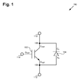
- FIG. 1 illustrates circuit 100, which can be implemented using a dual compartment semiconductor package, according to one embodiment of the invention.
- Circuit 100 comprises IGBT 102 and diode 104.
- diode 104 is connected in parallel with IGBT 102.
- Diode 104 has cathode C D and anode A D .
- IGBT 102 has collector C IGBT and emitter E IGBT .
- cathode C D of diode 104 is connected to collector C IGBT of IGBT 102 at node 106, which is connected to terminal 110.
- anode A D of diode 104 is connected to emitter E IGBT of IGBT 102 at node 108, which is connected to terminal 112.
- IGBT 102 also has gate G IGBT connected to terminal 114.
- Circuit 100 shows IGBT 102 and diode 104 being antiparallel, however, in other embodiments cathode C D can be connected to emitter E IGBT and anode A D can be connected to collector C IGBT .
- IGBT 102 can comprise a power switch and diode 104 can comprise a freewheeling diode.
- circuit 100 can comprise a high-side, or a low-side power switch in a phase of a three-phase motor drive.
- Figure 2 illustrates a cross section of package 200, according to one embodiment of the invention.
- Package 200 is a dual compartment semiconductor package.
- package 200 includes conductive clip 216, IGBT die 202, and diode die 204.
- conductive clip 216 is a metal clip and more particularly a copper clip.
- Conductive clip 216 has compartments 222 and 228, webs 224 and 230, walls 226a, 226b, 232a, and 232b, extension portions 234a, 234b, 234c, and 234d, contact portions 236a, 236b, and 236c, and groove 240.
- IGBT die 202 comprises gate electrode 258 and emitter electrode 260 on bottom surface 244 and connected collector electrode 246 on top surface 242.
- IGBT die 202 can correspond to IGBT 102 in Figure 1 .
- gate electrode 258 can correspond to gate G IGBT
- emitter electrode 260 can correspond to emitter E IGBT
- connected collector electrode 246 can correspond to C IGBT in Figure 1 .
- IGBT die 202 can comprise a plurality of respective gate, emitter, and collector electrodes.
- bottom surface 244 can comprise solderable front metal (SFM).
- Diode die 204 comprises anode electrode 262 on bottom surface 252 and connected cathode electrode 254 on top surface 250.
- Diode die 204 can correspond to diode 104 in Figure 1 .
- anode electrode 262 can correspond to anode A D and connected cathode electrode 254 can correspond to cathode C D in Figure 1 .
- IGBT die 202 can comprise a plurality of respective anode and cathode electrodes.
- bottom surface 252 can comprise SFM.
- Package 200 is electrically connecting respective top surfaces 242 and 250 of IGBT die 202 and diode die 204. More particularly, a collector of IGBT die 202 is electrically connected to compartment 222 through top surface 242 of IGBT die 202 and a cathode of diode die 204 is electrically connected to compartment 228 through top surface 250 of diode die 204.
- compartment 222 is electrically and mechanically connected to top surface 242 of IGBT die 202.
- package 200 includes connected collector electrode 246, which is electrically and mechanically connected to compartment 222 and comprises conductive material such as solder or conductive epoxy, for example silver-loaded epoxy, and die attach material 248 mechanically connecting top surface 242 and compartment 222.
- IGBT die 202 can comprise a plurality of connected collector electrodes on top surface 242.
- compartment 228 is electrically and mechanically connected to top surface 250 of diode die 204.
- package 200 includes connected cathode electrode 254, which is electrically and mechanically connected to compartment 228 and comprises conductive material such as solder or conductive epoxy, for example silver-loaded epoxy, and die attach material 256 mechanically connecting top surface 250 and compartment 228.
- conductive layer 254 is electrically connecting compartment 228 and a cathode of diode die 204.
- diode die 204 can comprise a plurality of connected cathode electrodes on top surface 250.
- contact portions 236a, 236b, and 236c each comprise a generally planar contact surface and can be used to connect package 200 to a substrate.
- contact portions 236a, 236b, and 236c can each make electrical and mechanical contact with conductive traces on the substrate.
- at least one of contact portions 23 6a, 23 6b, and 236c, particularly contact portion 236b, may not make electrical and/or mechanical contact with the conductive traces.
- contact portions 236a, 236b, and 236c are coplanar in the present embodiment, in some embodiments only contact portions 236a and 236c may be coplanar.
- contact portion 236b can be disposed above bottom surfaces 244 and 252 and contact portions 236a and 236c.
- extension portions 234b and 234c and contact portion 236b can be continuous and unitary.
- bottom surfaces of contact portions 236a, 236b, and 236c are coplanar with one another and with bottom surfaces 244 and 252 of IGBT die 202 and diode die 204.
- bottom surfaces 244 and 252 may be disposed above at least one of the bottom surfaces of contact portions 236a, 236b, and 236c.
- conductive clip 216 includes extension portions 234a, 234b, 234c, and 234d connecting and laterally separating contact portions 236a, 236b, and 236c and walls 226a, 226b, 232a, and 232b.
- extension portion 234b connects and laterally separates contact portion 236b and wall 226b
- extension portion 234c connects and laterally separates contact portion 236b and wall 232a.
- package 200 does not include at least one of extension portions 234a, 234b, 234c, and 234d.
- contact portion 236a can be directly connected to wall 226a
- contact portion 236b can be directly connected to walls 226b and 232a
- contact portion 236c can be directly connected to wall 232b.
- contact portions 236a, 236b, and 236c may not be disposed lateral to walls 226a, 236b, and 236c as shown in Figure 2 . Rather, for example, contact portion 236a can be disposed under wall 226a and can be continuous and unitary with wall 226a.
- groove 240 is formed between compartments 222 and 228 and can prevent electrical contact between respective bottom surfaces 244 and 252 of IGBT die 202 and diode die 204.
- groove 240 comprises a trench defined by contact portion 236b, extension portions 234b and 234c, wall 226b of compartment 222, and wall 232a of compartment 228.
- Contact portion 236b is under groove 240.
- the particular structure of groove 240 shown and described with respect to Figure 2 is not intended to limit groove 240.
- groove 240 can be rounded or triangular as specific examples.
- groove 240 may not include contact portion 236b and/or extension portions 234b and 234c.
- the top surfaces of webs 224 and 230 are coplanar and groove 240 extends below webs 224 and 230.
- groove 240 can prevent electrical contact between respective bottom surfaces 244 and 252 of IGBT die 202 and diode die 204.
- groove 240 can maintain separation between IGBT die 202 and diode die 204.
- the risk of electrical shorting due to the failure of device interconnects and movement of IGBT die 202 and diode die 204 can be substantially reduced in relation to conventional approaches.
- the IGBT has an external temperature sensor, the temperature sensor can be difficult to place in good thermal contact with the IGBT and can also interfere with placement of the heat sink and other components.
- IGBT die 202 and diode die 204 can be interconnected without bond wires and with short lead lengths and distances between the devices.
- package 200 can have a small footprint, high current carrying capability, low inductance, and low resistance.
- package 200 allows for convenient placement of an optional external temperature sensor and/or heat sink. Without bone wires, the heat sink can be arranged to have good thermal contact to IGBT die 202 and/or diode die 204 through top surfaces 242 and/or 250.
- IGBT die 202 and/or diode die 204 can be electrically and mechanically connected to compartments 222 and 228 in a manner different from the embodiment shown and described with respect to Figure 2 .
- anode electrode 262 can be on top surface 250 of diode die 204.
- Figure 2 shows IGBT die 202 and diode die 204, in other embodiments IGBT die 202 and diode die 204 can comprise other electrical components and do not necessarily comprise an IGBT and a diode respectively.
- Figure 3 illustrates a top view of package 300, according to one embodiment of the invention.
- Cross section 2-2 indicated in Figure 3 can correspond to the cross section of package 200 shown in Figure 2 .
- Figure 3 shows conductive clip 316, webs 324 and 330, walls 326a, 326b, 332a, and 332b, extension portions 334a, 334b, 334c, and 334d, contact portions 336a, 336b, and 336c, IGBT die 302, and diode die 304 corresponding respectively to conductive clip 216, webs 224 and 230, walls 226a, 226b, 232a, and 232b, extension portions 234a, 234b, 234c, and 234d, contact portions 236a, 236b, and 236c, IGBT die 202, and diode die 204 in Figure 2 .
- IGBT die 302 and diode die 304 are disposed under respective webs 324 and 330 and are indicated by respective
- package 300 is a dual can semiconductor package including cans 364 and 366.
- Can 364 includes web 324 and walls 326a, 326b, 326c, and 326d, which extend down from web 324 and surround IGBT die 302.
- Can 366 includes web 330 and walls 332a, 332b, 332c, and 332d, which extend down from web 330 and surround diode die 304. Dashed lines in Figure 3 indicate -inner boundaries of walls 226a, 226b, 226c, 226d, 332a, 332b, 332c, and 332d.
- groove 340 is formed between can 364 and 366.
- Groove 340 can separate IGBT die 302 and diode die 304.
- groove 340 extends along the length of cans 364 and 366.
- groove 340 may not be continuous as shown in Figure 3 and may not completely separate cans 364 and 366.
- Figure 3 shows cans 364 and 366 as being the same size, cans 364 and 366 can be different sizes with respect to one another.
- IGBT die 302 and diode die 304 can be different sizes with respect to each other and cans 364 and 366.
- package 300 does not include walls 326c, 326d, 332c, and 332d, but still may include walls 326a, 326b, 332a, and 332b.
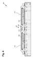
- Figure 4 illustrates a cross section of package 400 mounted on substrate 470, according to one embodiment of the invention.
- Package 400 can correspond to package 200 mounted on a substrate.
- Figure 4 shows IGBT die 402, diode die 404, and conductive clip 416 corresponding respectively to IGBT die 202, diode die 204, and conductive clip 216 in Figure 2 .
- Figure 4 also shows substrate 470 having conductive traces 472a, 472b, 472c, 472d, 472e, and 472f (also referred to herein as conductive traces 472a-f) formed thereon.
- Substrate 470 can comprise, for example, ceramic, aluminum nitride, or other substrate materials.
- conductive traces 472a-f can comprise copper bonded to substrate 470 to form a direct bonded copper (DBC) structure.
- DBC direct bonded copper
- Figure 4 also shows connected contact portions 474a, 474d, and 474f, which correspond to contact portions 236a, 236b, and 236c in Figure 2 connected to respective conductive traces 472a, 472d, and 472f.
- Connected contact portions 474a, 474d, and 474f are electrically and mechanically connected to substrate 470 and comprise conductive material such as solder or conductive epoxy, for example silver-loaded epoxy.
- Figure 4 also shows connected gate electrode 474b, connected emitter electrode 474c, and connected anode electrode 474e, corresponding to gate electrode 258, emitter electrode 260, and anode electrode 262 in Figure 2 connected to respective conductive traces 472b, 472c, and 472e.
- Connected gate electrode 474b, connected emitter electrode 474c, and connected anode electrode 474e are electrically and mechanically connected to substrate 470 and comprise conductive material such as solder or conductive epoxy, for example silver-loaded epoxy.
- IGBT die 402 and diode die 404 can comprise SFM.
- Package 400 enables IGBT die 402 and diode die 404 to be interconnected with short lead lengths and distances between the devices.
- conductive clip 416 corresponds to node 106 in Figure 1 .
- Conductive traces 472c and 472e are electrically connected, can comprise a single conductive trace on substrate 470, and collectively correspond to node 108 in Figure 1 .
- conductive trace 472b corresponds to terminal 114 in Figure 1 .
- IGBT die 402 and diode die 404 can be interconnected to form circuit 100 in Figure 1 .
- connected contact portion 474d which is under groove 440, is connected to substrate 470.
- connected contact portion 474d which is under groove 440, is electrically connected to conductive trace 472d on substrate 470 and is configured as an electrical contact of package 400, which advantageously reduces contact resistance.
- IGBT die 402 and diode die 404 may become very hot, for example, during operation as a power switch.
- connected gate electrode 474b, connected emitter electrode 474c, and connected anode electrode 474e may fail allowing for IGBT die 402 and diode die 404 to move.
- groove 440 can advantageously maintain separation between IGBT die 402 and diode die 404.
- groove 440 can prevent electrical contact between respective bottom surfaces of IGBT die 402 and diode die 404. As such, the risk of electrical shorting due to the failure of device interconnects and movement of IGBT die 402 and diode die 404 can minimized.
- package 200 allows for convenient placement of an optional external temperature sensor.
- package 400 includes temperature sensor 476 that is disposed within groove 440 and below the top surface of package 400 (in some embodiments, temperature sensor 476, can be placed over groove 440 or, in general, adjacent to groove 440).
- temperature sensor 476 can measure a temperature of IGBT die 402.
- temperature sensor 476 can measure a temperature of diode die 404.
- Temperature sensor 476 can comprise any suitable temperature sensor, such as a positive temperature coefficient (PTC) thermistor, a negative temperature coefficient (NTC) thermistor, and a chip resistor.
- PTC positive temperature coefficient
- NTC negative temperature coefficient
- Figure 4 shows temperature sensor 476 embedded in filler material 478, which can fill groove 440.
- Filler material 478 can be deposited over temperature sensor 476 and planarized.
- filler material 478 comprises thermally conductive material.
- filler material 478 comprises electrically conductive material.
- filler material 478 comprises thermally and/or electrically insulating material.
- package 400 includes temperature sensor 476 external to IGBT die 402 configured to monitor a temperature of IGBT die 402. As temperature sensor 476 is external to IGBT die 402, the size and manufacturing cost of IGBT die 402 can be reduced. Additionally, temperature sensor 476 can accurately measure a temperature without substantial interference from a noisy environment produced by switching IGBT die 402. Also, by including groove 440, temperature sensor 476 can be easily placed without increasing the size of package 400 and without interfering with placement of other components. For example, by including temperature sensor 476 within groove 440, an optional heat sink can easily be connected to package 400, which will be described in further detail with respect to figure 5 .
- Figure 5 illustrates a cross section of package 500 mounted on substrate 570, according to one embodiment of the invention.
- Package 500 can correspond to package 200 in Figure 2 and package 400 in Figure 4 .
- Figure 5 shows IGBT die 502, diode die 504, conductive clip 516, webs 524 and 530, compartments 522 and 528, groove 540, top surfaces 542 and 550, connected collector electrode 546, connected cathode electrode 554, and substrate 570 corresponding respectively to IGBT die 202, diode die 204, conductive clip 216, webs 224 and 230, compartments 222 and 228, groove 240, top surfaces 242 and 250, connected collector electrode 246, connected cathode electrode 254 in Figure 2 .
- Figure 5 also shows substrate 570 corresponding to substrate 470 in Figure 4 .
- Heat sink 580 situated over groove 540.
- heat sink 580 has bottom surface 584, which is coplanar with top surfaces of webs 524 and 530.
- Heat sink 580 can comprise any suitable heat sink, and can comprise one or more layers including a metal, a metal alloy, a metal oxide, a metal nitride, a ceramic material, an organic material, and combinations thereof.
- heat sink 580 comprises a DBC heat sink.
- Heat sink 580 is thermally connected to compartments 522 and 528 of conductive clip 516.
- IGBT die 502 and diode die 504 are also thermally connected to compartments 522 and 528 of conductive clip 516.
- connected collector electrode 546 and connected cathode electrode 554 each comprise thermally conductive material which can cover the majority of respective top surfaces 542 and 550.
- IGBT die 502 and diode die 504 are in good thermal contact with conductive clip 516 and heat sink 580.
- temperature sensor 576 can measure a temperature of IGBT die 502 while remaining external to IGBT die 502. Furthermore, because temperature sensor 576 is within groove 540, heat sink 580 can easily be connected to package 500. As shown in Figure 5 , heat sink 580 is over temperature sensor 576.
- Figure 5 shows filler materials 578 and 582 in groove 540. In the present embodiment filler material 578 is thermally conductive and can be electrically insulative. Thus, thermal contact with conductive clip 516 can be improved. However, filler material 582 is thermally insulative and is configured to thermally insulate temperature sensor 576 and heat sink 580.
- filler material 582 can improve the accuracy of a temperature measurment of IGBT die 502.
- temperature sensor 576 can be thermally and electrically insulated from heat sink 580 by an air pocket (not shown in Figure 5 ).
- heat sink 580 can be thermally connected to conductive clip 516 and thermally insulated from temperature sensor 576.
- some embodimnets may include heat sink 580 without temperature sensor 576.
- groove 240 can still optionally include filler material 582 and/or 578.
- heat sink 580 is not electrically connected to conductive clip 516 and is over webs 524 and 530.
- heat sink 580 can protect package 500 from electrical by covering webs 524 and 530, which are electrically conductive.
- heat sink 580 can provide rigidity to package 500 and can abate heating of package 500 to reduce the risk of interconnect failure.
- the present invention can provide for a dual compartment semiconductor package for an IGBT and a diode.
- the dual compartment semiconductor package can include a groove formed between first and second compartments to prevent electrical contact between respective bottom surfaces of the IGBT and the diode by maintaining separation between the IGBT and the diode. As such, the risk of electrical shorting due to failure of device interconnects and movement of the IGBT and the diode can be minimized.
- the dual compartment semiconductor package can allow for interconnection between the IGBT and the diode without bond wires.
- An external temperature sensor can optionally be situated over the groove for measuring a temperature of the dual compartment semiconductor package. The external temperature sensor is convinient to place without increasing the size of the dual compartment semiconductor package. Also, an optional heat sink can easily be thermally connected to the IGBT and the diode.
Landscapes
- Physics & Mathematics (AREA)
- General Physics & Mathematics (AREA)
- Cooling Or The Like Of Semiconductors Or Solid State Devices (AREA)
- Semiconductor Integrated Circuits (AREA)
Abstract
Description
- The present invention is generally in the field of semiconductors. More particularly, the invention relates to the packaging of semiconductor dies.
- An insulated-gate bipolar transistor (IGBT) can be connected to a freewheeling diode when implementing a power switch in a high power application, such as in a three-phase motor drive. In one approach to connecting the IGBT and the diode, the devices can be included in a common package, or a co-package. For example, a co-package can include the IGBT and the diode on a common substrate in close proximity. However, the IGBT and the diode may move resulting in undesirable contact and reduced reliability. For example, the IGBT and the diode may become very hot, resulting in failure of the contact to the common substrate. In another approach, the IGBT and the diode can be in separate packages to reduce the risk of movement of the IGBT and the diode. However, utilizing separate packages increases distances between the IGBT and the diode, resulting in a higher inductance connection between the devices. Furthermore, bond wires are typically employed as interconnects, resulting in reduced current carrying capability, higher inductance, and higher resistance.
- In order to avoid excessive heating, a temperature sensor may monitor the temperature of the IGBT, and a heat sink may dissipate heat from the IGBT and the diode. Where the IGBT has an external temperature sensor, the temperature sensor can be difficult to place in good thermal contact with the IGBT and can also interfere with placement of the heat sink and other components. Thus, an internal temperature sensor is typically included with the IGBT. The internal temperature sensor is monolithically formed with IGBT so that the temperature sensor is in good thermal contact with the IGBT while being unobtrusive to placement of the heat sink another the other components. However, including the internal temperature sensor with the IGBT increases the size of the IGBT and, moreover, accurate measurement of the temperature signal is difficult due to a noisy environment produced by switching the IGBT. Furthermore, the internal temperature sensor requires an extra mask layer during fabrication of the IGBT, thereby increasing manufacturing cost.
- Thus, it would be desirable to provide an IGBT with a diode in a higher reliability package, while avoiding the risk of the devices moving; and it would be further desirable to include a temperature sensor that does not interfere with placement of a heat sink and other components.
- A dual compartment semiconductor package with temperature sensor, substantially as shown in and/or described in connection with at least one of the figures, as set forth more completely in the claims.
-
-
Figure 1 illustrates an exemplary circuit, which can be implemented using a dual compartment semiconductor package, according to one embodiment of the invention. -
Figure 2 illustrates a cross section of an exemplary dual compartment semiconductor package, according to one embodiment of the invention. -
Figure 3 illustrates a top view of an exemplary dual compartment semiconductor package, according to one embodiment of the invention. -
Figure 4 illustrates a cross section of an exemplary dual compartment semiconductor package mounted on a substrate, according to one embodiment of the invention. -
Figure 5 illustrates a cross section of an exemplary dual compartment semiconductor package mounted on a substrate, according to one embodiment of the invention. - The present invention is directed to a dual compartment semiconductor package with temperature sensor. The following description contains specific information pertaining to the implementation of the present invention. One skilled in the art will recognize that the present invention may be implemented in a manner different from that specifically discussed in the present application. Moreover, some of the specific details of the invention are not discussed in order to not obscure the invention. The specific details not described in the present application are within the knowledge of a person of ordinary skill in the art.
- The drawings in the present application and their accompanying detailed description are directed to merely exemplary embodiments of the invention. To maintain brevity, other embodiments of the invention that use the principles of the present invention are not specifically described in the present application and are not specifically illustrated by the present drawings.
-
Figure 1 illustratescircuit 100, which can be implemented using a dual compartment semiconductor package, according to one embodiment of the invention.Circuit 100 comprises IGBT 102 anddiode 104. As shown inFigure 1 ,diode 104 is connected in parallel withIGBT 102.Diode 104 has cathode CD and anode AD. IGBT 102 has collector CIGBT and emitter EIGBT. Incircuit 100, cathode CD ofdiode 104 is connected to collector CIGBT of IGBT 102 atnode 106, which is connected toterminal 110. Also incircuit 100, anode AD ofdiode 104 is connected to emitter EIGBT ofIGBT 102 atnode 108, which is connected toterminal 112. IGBT 102 also has gate GIGBT connected toterminal 114.Circuit 100 shows IGBT 102 anddiode 104 being antiparallel, however, in other embodiments cathode CD can be connected to emitter EIGBT and anode AD can be connected to collector CIGBT. In one embodiment, IGBT 102 can comprise a power switch anddiode 104 can comprise a freewheeling diode. For example,circuit 100 can comprise a high-side, or a low-side power switch in a phase of a three-phase motor drive. -
Figure 2 illustrates a cross section ofpackage 200, according to one embodiment of the invention.Package 200 is a dual compartment semiconductor package. As shown inFigure 2 ,package 200 includesconductive clip 216,IGBT die 202, and diode die 204. In the present embodiment,conductive clip 216 is a metal clip and more particularly a copper clip.Conductive clip 216 hascompartments webs walls extension portions contact portions groove 240. - IGBT die 202 comprises
gate electrode 258 andemitter electrode 260 onbottom surface 244 and connectedcollector electrode 246 ontop surface 242. IGBT die 202 can correspond to IGBT 102 inFigure 1 . Thus,gate electrode 258 can correspond to gate GIGBT,emitter electrode 260 can correspond to emitter EIGBT and connectedcollector electrode 246 can correspond to CIGBT inFigure 1 . In some embodiments IGBT die 202 can comprise a plurality of respective gate, emitter, and collector electrodes. Also, in some embodiments,bottom surface 244 can comprise solderable front metal (SFM). - Diode die 204 comprises
anode electrode 262 onbottom surface 252 and connectedcathode electrode 254 ontop surface 250. Diode die 204 can correspond todiode 104 inFigure 1 . Thus,anode electrode 262 can correspond to anode AD and connectedcathode electrode 254 can correspond to cathode CD inFigure 1 . In some embodiments IGBT die 202 can comprise a plurality of respective anode and cathode electrodes. Also, in some embodiments,bottom surface 252 can comprise SFM. -
Package 200 is electrically connecting respectivetop surfaces compartment 222 throughtop surface 242 of IGBT die 202 and a cathode of diode die 204 is electrically connected tocompartment 228 throughtop surface 250 of diode die 204. - As shown in
Figure 2 ,walls web 224 to definecompartment 222.Compartment 222 is electrically and mechanically connected totop surface 242 ofIGBT die 202. As shown inFigure 2 ,package 200 includes connectedcollector electrode 246, which is electrically and mechanically connected tocompartment 222 and comprises conductive material such as solder or conductive epoxy, for example silver-loaded epoxy, and dieattach material 248 mechanically connectingtop surface 242 andcompartment 222. In some embodiments, IGBT die 202 can comprise a plurality of connected collector electrodes ontop surface 242. - Also shown in
Figure 2 ,walls web 230 to definecompartment 228.Compartment 228 is electrically and mechanically connected totop surface 250 of diode die 204. As shown inFigure 2 ,package 200 includes connectedcathode electrode 254, which is electrically and mechanically connected tocompartment 228 and comprises conductive material such as solder or conductive epoxy, for example silver-loaded epoxy, and die attachmaterial 256 mechanically connectingtop surface 250 andcompartment 228. In the present embodiment,conductive layer 254 is electrically connectingcompartment 228 and a cathode of diode die 204. In some embodiments, diode die 204 can comprise a plurality of connected cathode electrodes ontop surface 250. - Also in
conductive clip 216,contact portions package 200 to a substrate. In some embodiments contactportions contact portion 236b, may not make electrical and/or mechanical contact with the conductive traces. Also, whilecontact portions portions contact portion 236b can be disposed abovebottom surfaces contact portions embodiments extension portions 234b and 234c andcontact portion 236b can be continuous and unitary. Also in the present embodiment, bottom surfaces ofcontact portions bottom surfaces bottom surfaces contact portions - In the present embodiment,
conductive clip 216 includesextension portions contact portions walls extension portion 234b connects and laterally separatescontact portion 236b andwall 226b and extension portion 234c connects and laterally separatescontact portion 236b andwall 232a. In some embodiments,package 200 does not include at least one ofextension portions contact portion 236a can be directly connected towall 226a,contact portion 236b can be directly connected towalls contact portion 236c can be directly connected towall 232b. Also in some embodiments contactportions walls Figure 2 . Rather, for example,contact portion 236a can be disposed underwall 226a and can be continuous and unitary withwall 226a. - In
conductive clip 216,groove 240 is formed betweencompartments bottom surfaces Figure 2 , groove 240 comprises a trench defined bycontact portion 236b,extension portions 234b and 234c,wall 226b ofcompartment 222, andwall 232a ofcompartment 228.Contact portion 236b is undergroove 240. The particular structure ofgroove 240 shown and described with respect toFigure 2 is not intended to limitgroove 240. For example, in other embodiments groove 240 can be rounded or triangular as specific examples. In some embodiments, groove 240 may not includecontact portion 236b and/orextension portions 234b and 234c. In the present embodiment, the top surfaces ofwebs groove 240 extends belowwebs - By forming
groove 240 betweencompartments bottom surfaces compartment 222 totop surface 242 of IGBT die 202 and electrically and mechanically connectingcompartment 228 totop surface 250 of diode die 204, IGBT die 202 and diode die 204 can be interconnected without bond wires and with short lead lengths and distances between the devices. Thus,package 200 can have a small footprint, high current carrying capability, low inductance, and low resistance. Also,package 200 allows for convenient placement of an optional external temperature sensor and/or heat sink. Without bone wires, the heat sink can be arranged to have good thermal contact to IGBT die 202 and/or diode die 204 throughtop surfaces 242 and/or 250. - It is noted that in other embodiments, IGBT die 202 and/or diode die 204 can be electrically and mechanically connected to
compartments Figure 2 . As an example, in oneembodiment anode electrode 262 can be ontop surface 250 of diode die 204. Furthermore, whileFigure 2 shows IGBT die 202 and diode die 204, in other embodiments IGBT die 202 and diode die 204 can comprise other electrical components and do not necessarily comprise an IGBT and a diode respectively. - Referring now to
Figure 3, Figure 3 illustrates a top view ofpackage 300, according to one embodiment of the invention. Cross section 2-2 indicated inFigure 3 can correspond to the cross section ofpackage 200 shown inFigure 2 .Figure 3 showsconductive clip 316,webs walls extension portions contact portions conductive clip 216,webs walls extension portions contact portions Figure 2 . InFigure 3 , IGBT die 302 and diode die 304 are disposed underrespective webs - According to one embodiment,
package 300 is a dual can semiconductorpackage including cans web 324 andwalls web 324 and surround IGBT die 302. Can 366 includesweb 330 andwalls web 330 and surround diode die 304. Dashed lines inFigure 3 indicate -inner boundaries ofwalls - As shown in
Figure 3 , groove 340 is formed betweencan groove 340 extends along the length ofcans Figure 3 and may not completelyseparate cans Figure 3 showscans cans cans package 300 does not includewalls walls - Turning now to
Figure 4, Figure 4 illustrates a cross section ofpackage 400 mounted onsubstrate 470, according to one embodiment of the invention.Package 400 can correspond to package 200 mounted on a substrate.Figure 4 shows IGBT die 402, diode die 404, andconductive clip 416 corresponding respectively to IGBT die 202, diode die 204, andconductive clip 216 inFigure 2 .Figure 4 also showssubstrate 470 havingconductive traces conductive traces 472a-f) formed thereon.Substrate 470 can comprise, for example, ceramic, aluminum nitride, or other substrate materials. In the present embodiment,conductive traces 472a-f can comprise copper bonded tosubstrate 470 to form a direct bonded copper (DBC) structure.Figure 4 showspackage 400 mounted to the DBC structure. -
Figure 4 also showsconnected contact portions portions Figure 2 connected to respectiveconductive traces Connected contact portions substrate 470 and comprise conductive material such as solder or conductive epoxy, for example silver-loaded epoxy.Figure 4 also showsconnected gate electrode 474b, connectedemitter electrode 474c, and connected anode electrode 474e, corresponding togate electrode 258,emitter electrode 260, andanode electrode 262 inFigure 2 connected to respectiveconductive traces gate electrode 474b, connectedemitter electrode 474c, and connectedanode electrode 474e are electrically and mechanically connected tosubstrate 470 and comprise conductive material such as solder or conductive epoxy, for example silver-loaded epoxy. In some embodiments IGBT die 402 and diode die 404 can comprise SFM. -
Package 400 enables IGBT die 402 and diode die 404 to be interconnected with short lead lengths and distances between the devices. In the present embodiment,conductive clip 416 corresponds tonode 106 inFigure 1 . Conductive traces 472c and 472e are electrically connected, can comprise a single conductive trace onsubstrate 470, and collectively correspond tonode 108 inFigure 1 . Also,conductive trace 472b corresponds to terminal 114 inFigure 1 . Thus, IGBT die 402 and diode die 404 can be interconnected to formcircuit 100 inFigure 1 . In the present embodiment, connectedcontact portion 474d, which is undergroove 440, is connected tosubstrate 470. InFigure 4 , connectedcontact portion 474d, which is undergroove 440, is electrically connected toconductive trace 472d onsubstrate 470 and is configured as an electrical contact ofpackage 400, which advantageously reduces contact resistance. - IGBT die 402 and diode die 404 may become very hot, for example, during operation as a power switch. As a result, connected
gate electrode 474b, connectedemitter electrode 474c, and connectedanode electrode 474e may fail allowing for IGBT die 402 and diode die 404 to move. However, groove 440 can advantageously maintain separation between IGBT die 402 and diode die 404. Thus, groove 440 can prevent electrical contact between respective bottom surfaces of IGBT die 402 and diode die 404. As such, the risk of electrical shorting due to the failure of device interconnects and movement of IGBT die 402 and diode die 404 can minimized. - As discussed above with respect to
Figure 2 ,package 200 allows for convenient placement of an optional external temperature sensor. In the present embodiment,package 400 includestemperature sensor 476 that is disposed withingroove 440 and below the top surface of package 400 (in some embodiments,temperature sensor 476, can be placed overgroove 440 or, in general, adjacent to groove 440). Astemperature sensor 476 is in good temperature contact withconductive clip 416, which itself is in good temperature contact with IGBT die 402,temperature sensor 476 can measure a temperature of IGBT die 402. In someembodiments temperature sensor 476 can measure a temperature of diode die 404.Temperature sensor 476 can comprise any suitable temperature sensor, such as a positive temperature coefficient (PTC) thermistor, a negative temperature coefficient (NTC) thermistor, and a chip resistor. -
Figure 4 showstemperature sensor 476 embedded infiller material 478, which can fillgroove 440.Filler material 478 can be deposited overtemperature sensor 476 and planarized. In someembodiments filler material 478 comprises thermally conductive material. Also in someembodiments filler material 478 comprises electrically conductive material. In someembodiments filler material 478 comprises thermally and/or electrically insulating material. - Thus, as shown in
Figure 4 ,package 400 includestemperature sensor 476 external to IGBT die 402 configured to monitor a temperature of IGBT die 402. Astemperature sensor 476 is external to IGBT die 402, the size and manufacturing cost of IGBT die 402 can be reduced. Additionally,temperature sensor 476 can accurately measure a temperature without substantial interference from a noisy environment produced by switching IGBT die 402. Also, by includinggroove 440,temperature sensor 476 can be easily placed without increasing the size ofpackage 400 and without interfering with placement of other components. For example, by includingtemperature sensor 476 withingroove 440, an optional heat sink can easily be connected to package 400, which will be described in further detail with respect tofigure 5 . - Referring now to
Figure 5, Figure 5 illustrates a cross section ofpackage 500 mounted onsubstrate 570, according to one embodiment of the invention.Package 500 can correspond to package 200 inFigure 2 andpackage 400 inFigure 4 .Figure 5 shows IGBT die 502, diode die 504,conductive clip 516,webs compartments groove 540,top surfaces collector electrode 546, connectedcathode electrode 554, andsubstrate 570 corresponding respectively to IGBT die 202, diode die 204,conductive clip 216,webs compartments groove 240,top surfaces collector electrode 246, connectedcathode electrode 254 inFigure 2 .Figure 5 also showssubstrate 570 corresponding tosubstrate 470 inFigure 4 . -
Figure 5 also showsheat sink 580 situated overgroove 540. In the present embodiment,heat sink 580 hasbottom surface 584, which is coplanar with top surfaces ofwebs Heat sink 580 can comprise any suitable heat sink, and can comprise one or more layers including a metal, a metal alloy, a metal oxide, a metal nitride, a ceramic material, an organic material, and combinations thereof. In oneembodiment heat sink 580 comprises a DBC heat sink.Heat sink 580 is thermally connected tocompartments conductive clip 516. IGBT die 502 and diode die 504 are also thermally connected tocompartments conductive clip 516. In the present embodiment, connectedcollector electrode 546 and connectedcathode electrode 554 each comprise thermally conductive material which can cover the majority of respectivetop surfaces conductive clip 516 andheat sink 580. - Also in the present embodiment, as IGBT die 502 and
temperature senor 576 are each in good thermal contact withconductive clip 516,temperature sensor 576 can measure a temperature of IGBT die 502 while remaining external to IGBT die 502. Furthermore, becausetemperature sensor 576 is withingroove 540,heat sink 580 can easily be connected to package 500. As shown inFigure 5 ,heat sink 580 is overtemperature sensor 576.Figure 5 showsfiller materials groove 540. In the presentembodiment filler material 578 is thermally conductive and can be electrically insulative. Thus, thermal contact withconductive clip 516 can be improved. However,filler material 582 is thermally insulative and is configured to thermally insulatetemperature sensor 576 andheat sink 580. As such,filler material 582 can improve the accuracy of a temperature measurment of IGBT die 502. In someembodimnets temperature sensor 576 can be thermally and electrically insulated fromheat sink 580 by an air pocket (not shown inFigure 5 ). Thus, as described above,heat sink 580 can be thermally connected toconductive clip 516 and thermally insulated fromtemperature sensor 576. It is noted that some embodimnets may includeheat sink 580 withouttemperature sensor 576. However, groove 240 can still optionally includefiller material 582 and/or 578. - In the present embodiment,
heat sink 580 is not electrically connected toconductive clip 516 and is overwebs heat sink 580 can protectpackage 500 from electrical by coveringwebs heat sink 580 can provide rigidity to package 500 and can abate heating ofpackage 500 to reduce the risk of interconnect failure. - Thus, as discussed above, in the embodiments of
Figures 1 through 5 , the present invention can provide for a dual compartment semiconductor package for an IGBT and a diode. The dual compartment semiconductor package can include a groove formed between first and second compartments to prevent electrical contact between respective bottom surfaces of the IGBT and the diode by maintaining separation between the IGBT and the diode. As such, the risk of electrical shorting due to failure of device interconnects and movement of the IGBT and the diode can be minimized. Also, the dual compartment semiconductor package can allow for interconnection between the IGBT and the diode without bond wires. An external temperature sensor can optionally be situated over the groove for measuring a temperature of the dual compartment semiconductor package. The external temperature sensor is convinient to place without increasing the size of the dual compartment semiconductor package. Also, an optional heat sink can easily be thermally connected to the IGBT and the diode. - From the above description of the invention it is manifest that various techniques can be used for implementing the concepts of the present invention without departing from its scope. Moreover, while the invention has been described with specific reference to certain embodiments, a person of ordinary skill in the art would appreciate that changes can be made in form and detail without departing from the spirit and the scope of the invention. Thus, the described embodiments are to be considered in all respects as illustrative and not restrictive. It should also be understood that the invention is not limited to the particular embodiments described herein but is capable of many rearrangements, modifications, and substitutions without departing from the scope of the invention.
Claims (16)
- A dual compartment semiconductor package comprising:a conductive clip having first and second compartments;said first compartment electrically and mechanically connected to a top surface of a first die;said second compartment electrically and mechanically connected to a top surface of a second die;a groove formed between said first and second compartments, said groove preventing contact between said first and second dies;said dual compartment package electrically connecting said top surface of said first die to said top surface of said second die.
- The dual compartment semiconductor package of claim 1, wherein said first die comprises an insulated-gate bipolar transistor (IGBT).
- The dual compartment semiconductor package of claim 1, wherein said second die comprises a diode.
- The dual compartment semiconductor package of claim 1, wherein said first die comprises an IGBT, a collector electrode of said IGBT on said top surface of said first die and a gate electrode and an emitter electrode of said IGBT on a bottom surface of said first die.
- The dual compartment semiconductor package of claim 1, wherein said conductive clip comprises a contact portion under said groove, said contact portion configured to connect to a substrate.
- The dual compartment semiconductor package of claim 1, comprising a temperature sensor situated over said groove for measuring a temperature of said dual compartment semiconductor package.
- The dual compartment semiconductor package of claim 1, comprising a heat sink over said groove.
- The dual compartment semiconductor package of claim 1, comprising a heat sink thermally connected to said first and second compartments.
- A dual compartment semiconductor package comprising:a conductive clip having first and second compartments;said first compartment electrically and mechanically connected to a top surface of said first die;said second compartment electrically and mechanically connected to a top surface of said second die;a groove formed between said first and second compartments;said dual compartment package electrically connecting said top surface of said first die to said top surface of said second die;a temperature sensor situated adjacent to said groove for measuring a temperature of said dual compartment semiconductor package.
- The dual compartment semiconductor package of claim 9, wherein said first die comprises an insulated-gate bipolar transistor (IGBT).
- The dual compartment semiconductor package of claim 9, wherein said second die comprises a diode.
- The dual compartment semiconductor package of claim 9, wherein said temperature sensor is external to said first die and is configured to measure a temperature of said first die.
- The dual compartment semiconductor package of claim 9, wherein said temperature sensor is within said groove.
- The dual compartment semiconductor package of claim 9, comprising a heat sink over said temperature sensor.
- The dual compartment semiconductor package of claim 9, comprising a heat sink thermally connected to said first and second compartments.
- The dual compartment semiconductor package of claim 9, comprising a heat sink thermally connected to said conductive clip and thermally insulated from said temperature sensor.
Applications Claiming Priority (1)
| Application Number | Priority Date | Filing Date | Title |
|---|---|---|---|
| US13/075,597 US8637981B2 (en) | 2011-03-30 | 2011-03-30 | Dual compartment semiconductor package with temperature sensor |
Publications (3)
| Publication Number | Publication Date |
|---|---|
| EP2506300A2 true EP2506300A2 (en) | 2012-10-03 |
| EP2506300A3 EP2506300A3 (en) | 2014-02-12 |
| EP2506300B1 EP2506300B1 (en) | 2019-10-16 |
Family
ID=45841173
Family Applications (1)
| Application Number | Title | Priority Date | Filing Date |
|---|---|---|---|
| EP12157061.8A Active EP2506300B1 (en) | 2011-03-30 | 2012-02-27 | Dual compartment semiconductor package |
Country Status (3)
| Country | Link |
|---|---|
| US (3) | US8637981B2 (en) |
| EP (1) | EP2506300B1 (en) |
| JP (1) | JP5684747B2 (en) |
Cited By (7)
| Publication number | Priority date | Publication date | Assignee | Title |
|---|---|---|---|---|
| GB2549934A (en) * | 2016-04-28 | 2017-11-08 | Reinhausen Maschf Scheubeck | Junction temperature and current sensing |
| EP3361506A1 (en) * | 2017-02-09 | 2018-08-15 | Kabushiki Kaisha Toshiba | Semiconductor module |
| NL2020927A (en) * | 2017-05-19 | 2018-11-23 | Shindengen Electric Mfg | Method of manufacturing chip module |
| NL2020926A (en) * | 2017-05-19 | 2018-11-23 | Shindengen Electric Mfg | Electronic module |
| NL2020939A (en) * | 2017-05-19 | 2018-11-23 | Shindengen Electric Mfg | Electronic module |
| EP2722885B1 (en) * | 2012-10-17 | 2020-03-25 | Infineon Technologies Americas Corp. | Surface mountable power components |
| EP4068349A1 (en) * | 2021-03-30 | 2022-10-05 | Siemens Aktiengesellschaft | Power module |
Families Citing this family (22)
| Publication number | Priority date | Publication date | Assignee | Title |
|---|---|---|---|---|
| US8350376B2 (en) * | 2011-04-18 | 2013-01-08 | International Rectifier Corporation | Bondwireless power module with three-dimensional current routing |
| US20130256894A1 (en) * | 2012-03-29 | 2013-10-03 | International Rectifier Corporation | Porous Metallic Film as Die Attach and Interconnect |
| WO2014080931A1 (en) * | 2012-11-21 | 2014-05-30 | 株式会社カネカ | Heat dissipation structure |
| US9437589B2 (en) * | 2014-03-25 | 2016-09-06 | Infineon Technologies Ag | Protection devices |
| DE102015200485A1 (en) * | 2015-01-14 | 2016-07-14 | Robert Bosch Gmbh | Contact arrangement and power module |
| US9911712B2 (en) * | 2015-10-26 | 2018-03-06 | Semiconductor Components Industries, Llc | Clip and related methods |
| US10068817B2 (en) * | 2016-03-18 | 2018-09-04 | Macom Technology Solutions Holdings, Inc. | Semiconductor package |
| US10580754B2 (en) * | 2016-04-01 | 2020-03-03 | Mitsubishi Electric Corporation | Semiconductor module with temperature detecting element |
| CN105789160B (en) * | 2016-05-03 | 2017-05-24 | 扬州国扬电子有限公司 | Combined electrode and three-level high power module thereof |
| CN112119492A (en) * | 2018-05-17 | 2020-12-22 | 京瓷株式会社 | Power semiconductor module |
| KR102519001B1 (en) | 2018-05-28 | 2023-04-10 | 삼성전자주식회사 | Film package and Package module including the same |
| US11088046B2 (en) * | 2018-06-25 | 2021-08-10 | Semiconductor Components Industries, Llc | Semiconductor device package with clip interconnect and dual side cooling |
| DE102019108988B3 (en) * | 2019-04-05 | 2020-08-13 | Infineon Technologies Ag | POWER SEMI-CONDUCTOR MODULE AND METHOD FOR MANUFACTURING THE SAME |
| JP7322654B2 (en) * | 2019-10-15 | 2023-08-08 | 富士電機株式会社 | semiconductor module |
| US11037917B1 (en) | 2019-12-11 | 2021-06-15 | Littelfuse, Inc. | Semiconductor device module and method of assembly |
| US11393743B2 (en) * | 2019-12-18 | 2022-07-19 | Infineon Technologies Ag | Semiconductor assembly with conductive frame for I/O standoff and thermal dissipation |
| CN112151418B (en) * | 2020-09-11 | 2024-04-05 | 安徽龙芯微科技有限公司 | Packaging mechanism and packaging method of silicon-based adapter plate |
| JP7734505B2 (en) * | 2021-04-06 | 2025-09-05 | 三菱重工業株式会社 | Semiconductor Devices |
| DE102021110609B4 (en) | 2021-04-26 | 2026-04-16 | Semikron Danfoss Elektronik Gmbh & Co. Kg | Power semiconductor module and method for fabricating a power semiconductor module |
| WO2023222195A1 (en) * | 2022-05-17 | 2023-11-23 | Hitachi Energy Switzerland Ag | Power module and method for producing a power module |
| KR20230168647A (en) * | 2022-06-07 | 2023-12-15 | 현대모비스 주식회사 | Power module |
| DE102024202740B3 (en) * | 2024-03-22 | 2025-05-22 | Zf Friedrichshafen Ag | Sensor device, method for producing a sensor device, power converter, electric axle drive and motor vehicle |
Family Cites Families (46)
| Publication number | Priority date | Publication date | Assignee | Title |
|---|---|---|---|---|
| JP3180863B2 (en) * | 1993-07-27 | 2001-06-25 | 富士電機株式会社 | Pressure contact type semiconductor device and method of assembling the same |
| US5757620A (en) * | 1994-12-05 | 1998-05-26 | International Business Machines Corporation | Apparatus for cooling of chips using blind holes with customized depth |
| US5604978A (en) * | 1994-12-05 | 1997-02-25 | International Business Machines Corporation | Method for cooling of chips using a plurality of materials |
| FR2732184B1 (en) * | 1995-03-21 | 1997-04-30 | Asulab Sa | ELECTRIC POWER MODULE |
| JPH09148492A (en) | 1995-11-17 | 1997-06-06 | Murata Mfg Co Ltd | Electronic component packaging equipment |
| US5706171A (en) * | 1995-11-20 | 1998-01-06 | International Business Machines Corporation | Flat plate cooling using a thermal paste retainer |
| US5981310A (en) * | 1998-01-22 | 1999-11-09 | International Business Machines Corporation | Multi-chip heat-sink cap assembly |
| US5926369A (en) * | 1998-01-22 | 1999-07-20 | International Business Machines Corporation | Vertically integrated multi-chip circuit package with heat-sink support |
| JP3596388B2 (en) * | 1999-11-24 | 2004-12-02 | 株式会社デンソー | Semiconductor device |
| JP3996315B2 (en) * | 2000-02-21 | 2007-10-24 | 松下電器産業株式会社 | Semiconductor device and manufacturing method thereof |
| US6541310B1 (en) * | 2000-07-24 | 2003-04-01 | Siliconware Precision Industries Co., Ltd. | Method of fabricating a thin and fine ball-grid array package with embedded heat spreader |
| JP3923258B2 (en) * | 2001-01-17 | 2007-05-30 | 松下電器産業株式会社 | Power control system electronic circuit device and manufacturing method thereof |
| DE10137619A1 (en) * | 2001-08-01 | 2003-02-27 | Infineon Technologies Ag | Cover element for assemblies |
| US6677669B2 (en) | 2002-01-18 | 2004-01-13 | International Rectifier Corporation | Semiconductor package including two semiconductor die disposed within a common clip |
| US6744640B2 (en) * | 2002-04-10 | 2004-06-01 | Gore Enterprise Holdings, Inc. | Board-level EMI shield with enhanced thermal dissipation |
| US6885101B2 (en) * | 2002-08-29 | 2005-04-26 | Micron Technology, Inc. | Methods for wafer-level packaging of microelectronic devices and microelectronic devices formed by such methods |
| TWI242861B (en) * | 2003-08-11 | 2005-11-01 | Siliconware Precision Industries Co Ltd | Multi-chip semiconductor package with heat sink and fabrication method thereof |
| JP2005116762A (en) * | 2003-10-07 | 2005-04-28 | Fujitsu Ltd | Semiconductor device protection method, semiconductor device cover, semiconductor device unit, and semiconductor device packaging structure |
| US6979899B2 (en) * | 2003-12-31 | 2005-12-27 | Texas Instruments Incorported | System and method for high performance heat sink for multiple chip devices |
| TWI278947B (en) | 2004-01-13 | 2007-04-11 | Samsung Electronics Co Ltd | A multi-chip package, a semiconductor device used therein and manufacturing method thereof |
| JP3809168B2 (en) * | 2004-02-03 | 2006-08-16 | 株式会社東芝 | Semiconductor module |
| TWI232568B (en) * | 2004-03-11 | 2005-05-11 | Advanced Semiconductor Eng | Multi package module with heat spreader |
| KR100686029B1 (en) | 2005-02-25 | 2007-02-22 | 엘지전자 주식회사 | Semiconductor chip fixing structure of electric heat sink |
| US8022512B2 (en) * | 2006-02-28 | 2011-09-20 | Unisem (Mauritus) Holdings Limited | No lead package with heat spreader |
| DE102006027481C5 (en) * | 2006-06-14 | 2012-11-08 | Semikron Elektronik Gmbh & Co. Kg | Power semiconductor module with mutually electrically insulated connection elements |
| JP5232367B2 (en) * | 2006-07-12 | 2013-07-10 | ルネサスエレクトロニクス株式会社 | Semiconductor device |
| US20080128897A1 (en) * | 2006-12-05 | 2008-06-05 | Tong Wa Chao | Heat spreader for a multi-chip package |
| CA2687120A1 (en) | 2007-05-08 | 2008-11-13 | Scanimetrics Inc. | Ultra high speed signal transmission/reception |
| JP4856014B2 (en) * | 2007-06-28 | 2012-01-18 | 三菱電機株式会社 | Circuit module and manufacturing method thereof |
| US20090057884A1 (en) * | 2007-08-29 | 2009-03-05 | Seah Sun Too | Multi-Chip Package |
| US8178956B2 (en) * | 2007-12-13 | 2012-05-15 | Stats Chippac Ltd. | Integrated circuit package system for shielding electromagnetic interference |
| US7800219B2 (en) * | 2008-01-02 | 2010-09-21 | Fairchild Semiconductor Corporation | High-power semiconductor die packages with integrated heat-sink capability and methods of manufacturing the same |
| JP5062005B2 (en) | 2008-04-03 | 2012-10-31 | 三菱電機株式会社 | Power semiconductor device |
| US8018032B2 (en) * | 2008-12-31 | 2011-09-13 | Unimicron Technology Corp. | Silicon substrate and chip package structure with silicon base having stepped recess for accommodating chip |
| US8202765B2 (en) * | 2009-01-22 | 2012-06-19 | International Business Machines Corporation | Achieving mechanical and thermal stability in a multi-chip package |
| JP5492447B2 (en) * | 2009-04-28 | 2014-05-14 | 日立オートモティブシステムズ株式会社 | Power module |
| US8563360B2 (en) | 2009-06-08 | 2013-10-22 | Alpha And Omega Semiconductor, Inc. | Power semiconductor device package and fabrication method |
| JP2011086889A (en) | 2009-10-19 | 2011-04-28 | Renesas Electronics Corp | Semiconductor device and manufacturing method thereof |
| US8586414B2 (en) * | 2010-12-14 | 2013-11-19 | Alpha & Omega Semiconductor, Inc. | Top exposed package and assembly method |
| US7939370B1 (en) * | 2009-10-29 | 2011-05-10 | Alpha And Omega Semiconductor Incorporated | Power semiconductor package |
| US8093714B2 (en) * | 2009-12-10 | 2012-01-10 | Semtech Corporation | Chip assembly with chip-scale packaging |
| US8138062B2 (en) | 2009-12-15 | 2012-03-20 | Freescale Semiconductor, Inc. | Electrical coupling of wafer structures |
| US8350381B2 (en) * | 2010-04-01 | 2013-01-08 | Infineon Technologies Ag | Device and method for manufacturing a device |
| US8299587B2 (en) * | 2010-04-21 | 2012-10-30 | Powertech Technology Inc. | Lead frame package structure for side-by-side disposed chips |
| US8519525B2 (en) * | 2010-07-29 | 2013-08-27 | Alpha & Omega Semiconductor, Inc. | Semiconductor encapsulation and method thereof |
| US8507316B2 (en) * | 2010-12-22 | 2013-08-13 | Taiwan Semiconductor Manufacturing Company, Ltd. | Protecting T-contacts of chip scale packages from moisture |
-
2011
- 2011-03-30 US US13/075,597 patent/US8637981B2/en not_active Expired - Fee Related
-
2012
- 2012-02-27 EP EP12157061.8A patent/EP2506300B1/en active Active
- 2012-02-28 JP JP2012042346A patent/JP5684747B2/en active Active
-
2014
- 2014-01-23 US US14/162,508 patent/US8860198B2/en active Active
- 2014-01-23 US US14/162,690 patent/US9054119B2/en active Active
Non-Patent Citations (1)
| Title |
|---|
| None |
Cited By (12)
| Publication number | Priority date | Publication date | Assignee | Title |
|---|---|---|---|---|
| EP2722885B1 (en) * | 2012-10-17 | 2020-03-25 | Infineon Technologies Americas Corp. | Surface mountable power components |
| GB2549934A (en) * | 2016-04-28 | 2017-11-08 | Reinhausen Maschf Scheubeck | Junction temperature and current sensing |
| EP3361506A1 (en) * | 2017-02-09 | 2018-08-15 | Kabushiki Kaisha Toshiba | Semiconductor module |
| US10199365B2 (en) | 2017-02-09 | 2019-02-05 | Kabushiki Kaisha Toshiba | Semiconductor module |
| NL2020927A (en) * | 2017-05-19 | 2018-11-23 | Shindengen Electric Mfg | Method of manufacturing chip module |
| NL2020926A (en) * | 2017-05-19 | 2018-11-23 | Shindengen Electric Mfg | Electronic module |
| NL2020939A (en) * | 2017-05-19 | 2018-11-23 | Shindengen Electric Mfg | Electronic module |
| US11189591B2 (en) | 2017-05-19 | 2021-11-30 | Shindengen Electric Manufacturing Co., Ltd. | Electronic module |
| US11264351B2 (en) | 2017-05-19 | 2022-03-01 | Shindengen Electric Manufacturing Co., Ltd. | Method of manufacturing chip module |
| US11276663B2 (en) | 2017-05-19 | 2022-03-15 | Shindengen Electric Manufacturing Co., Ltd. | Electronic module |
| EP4068349A1 (en) * | 2021-03-30 | 2022-10-05 | Siemens Aktiengesellschaft | Power module |
| US12068209B2 (en) | 2021-03-30 | 2024-08-20 | Siemens Aktiengesellschaft | Power module |
Also Published As
| Publication number | Publication date |
|---|---|
| JP5684747B2 (en) | 2015-03-18 |
| US20120248564A1 (en) | 2012-10-04 |
| EP2506300A3 (en) | 2014-02-12 |
| US9054119B2 (en) | 2015-06-09 |
| EP2506300B1 (en) | 2019-10-16 |
| US8637981B2 (en) | 2014-01-28 |
| US20140131767A1 (en) | 2014-05-15 |
| JP2012212863A (en) | 2012-11-01 |
| US8860198B2 (en) | 2014-10-14 |
| US20140131709A1 (en) | 2014-05-15 |
Similar Documents
| Publication | Publication Date | Title |
|---|---|---|
| EP2506300B1 (en) | Dual compartment semiconductor package | |
| JP5001637B2 (en) | Package for high power density devices | |
| KR101909948B1 (en) | Multi-level options for power mosfets | |
| CN104517939B (en) | vertical shunt resistance | |
| US20110073984A1 (en) | Semiconductor power module package with temperature sensor mounted thereon and method of fabricating the same | |
| US11610830B2 (en) | Power semiconductor module and method for fabricating the same | |
| US8373197B2 (en) | Circuit device | |
| KR102588063B1 (en) | Semiconductor package having symmetrically arranged power terminals and method for producing same | |
| KR20150026942A (en) | Electronic device | |
| CN110299341A (en) | Semiconductor devices and electronic device | |
| US20240413148A1 (en) | Isolated 3d semiconductor device package with transistors attached to opposing sides of leadframe sharing leads | |
| US20240429138A1 (en) | Semiconductor device | |
| CN112968027A (en) | Intelligent power module | |
| US20040016979A1 (en) | Semiconductor device | |
| US20240321693A1 (en) | Semiconductor device | |
| US11646249B2 (en) | Dual-side cooling semiconductor packages and related methods | |
| US9373566B2 (en) | High power electronic component with multiple leadframes | |
| CN113161337A (en) | Intelligent power module | |
| CN216145614U (en) | Intelligent power module | |
| CN115116983A (en) | Power semiconductor device with temperature sensor integrated on back surface and preparation method | |
| CN113035856A (en) | Intelligent power module | |
| CN210006735U (en) | Mosfet semiconductor device with internal integrated temperature protection device | |
| CN219106135U (en) | Molded power semiconductor package | |
| CN112768503A (en) | IGBT chip, manufacturing method thereof and power module | |
| CN222762964U (en) | Semiconductor packaging structure and electronic equipment |
Legal Events
| Date | Code | Title | Description |
|---|---|---|---|
| PUAI | Public reference made under article 153(3) epc to a published international application that has entered the european phase |
Free format text: ORIGINAL CODE: 0009012 |
|
| AK | Designated contracting states |
Kind code of ref document: A2 Designated state(s): AL AT BE BG CH CY CZ DE DK EE ES FI FR GB GR HR HU IE IS IT LI LT LU LV MC MK MT NL NO PL PT RO RS SE SI SK SM TR |
|
| AX | Request for extension of the european patent |
Extension state: BA ME |
|
| RIC1 | Information provided on ipc code assigned before grant |
Ipc: H01L 23/492 20060101ALI20130916BHEP Ipc: H01L 23/34 20060101AFI20130916BHEP |
|
| PUAL | Search report despatched |
Free format text: ORIGINAL CODE: 0009013 |
|
| AK | Designated contracting states |
Kind code of ref document: A3 Designated state(s): AL AT BE BG CH CY CZ DE DK EE ES FI FR GB GR HR HU IE IS IT LI LT LU LV MC MK MT NL NO PL PT RO RS SE SI SK SM TR |
|
| AX | Request for extension of the european patent |
Extension state: BA ME |
|
| RIC1 | Information provided on ipc code assigned before grant |
Ipc: H01L 23/492 20060101ALI20140103BHEP Ipc: H01L 23/34 20060101AFI20140103BHEP |
|
| 17P | Request for examination filed |
Effective date: 20140812 |
|
| RBV | Designated contracting states (corrected) |
Designated state(s): AL AT BE BG CH CY CZ DE DK EE ES FI FR GB GR HR HU IE IS IT LI LT LU LV MC MK MT NL NO PL PT RO RS SE SI SK SM TR |
|
| STAA | Information on the status of an ep patent application or granted ep patent |
Free format text: STATUS: EXAMINATION IS IN PROGRESS |
|
| 17Q | First examination report despatched |
Effective date: 20171020 |
|
| RAP1 | Party data changed (applicant data changed or rights of an application transferred) |
Owner name: INFINEON TECHNOLOGIES AMERICAS CORP. |
|
| GRAP | Despatch of communication of intention to grant a patent |
Free format text: ORIGINAL CODE: EPIDOSNIGR1 |
|
| STAA | Information on the status of an ep patent application or granted ep patent |
Free format text: STATUS: GRANT OF PATENT IS INTENDED |
|
| INTG | Intention to grant announced |
Effective date: 20190503 |
|
| GRAS | Grant fee paid |
Free format text: ORIGINAL CODE: EPIDOSNIGR3 |
|
| GRAA | (expected) grant |
Free format text: ORIGINAL CODE: 0009210 |
|
| STAA | Information on the status of an ep patent application or granted ep patent |
Free format text: STATUS: THE PATENT HAS BEEN GRANTED |
|
| AK | Designated contracting states |
Kind code of ref document: B1 Designated state(s): AL AT BE BG CH CY CZ DE DK EE ES FI FR GB GR HR HU IE IS IT LI LT LU LV MC MK MT NL NO PL PT RO RS SE SI SK SM TR |
|
| REG | Reference to a national code |
Ref country code: GB Ref legal event code: FG4D |
|
| REG | Reference to a national code |
Ref country code: CH Ref legal event code: EP |
|
| REG | Reference to a national code |
Ref country code: DE Ref legal event code: R096 Ref document number: 602012064847 Country of ref document: DE |
|
| REG | Reference to a national code |
Ref country code: IE Ref legal event code: FG4D |
|
| REG | Reference to a national code |
Ref country code: AT Ref legal event code: REF Ref document number: 1192127 Country of ref document: AT Kind code of ref document: T Effective date: 20191115 |
|
| REG | Reference to a national code |
Ref country code: NL Ref legal event code: MP Effective date: 20191016 |
|
| REG | Reference to a national code |
Ref country code: LT Ref legal event code: MG4D |
|
| REG | Reference to a national code |
Ref country code: AT Ref legal event code: MK05 Ref document number: 1192127 Country of ref document: AT Kind code of ref document: T Effective date: 20191016 |
|
| PG25 | Lapsed in a contracting state [announced via postgrant information from national office to epo] |
Ref country code: FI Free format text: LAPSE BECAUSE OF FAILURE TO SUBMIT A TRANSLATION OF THE DESCRIPTION OR TO PAY THE FEE WITHIN THE PRESCRIBED TIME-LIMIT Effective date: 20191016 Ref country code: BG Free format text: LAPSE BECAUSE OF FAILURE TO SUBMIT A TRANSLATION OF THE DESCRIPTION OR TO PAY THE FEE WITHIN THE PRESCRIBED TIME-LIMIT Effective date: 20200116 Ref country code: PT Free format text: LAPSE BECAUSE OF FAILURE TO SUBMIT A TRANSLATION OF THE DESCRIPTION OR TO PAY THE FEE WITHIN THE PRESCRIBED TIME-LIMIT Effective date: 20200217 Ref country code: LT Free format text: LAPSE BECAUSE OF FAILURE TO SUBMIT A TRANSLATION OF THE DESCRIPTION OR TO PAY THE FEE WITHIN THE PRESCRIBED TIME-LIMIT Effective date: 20191016 Ref country code: NO Free format text: LAPSE BECAUSE OF FAILURE TO SUBMIT A TRANSLATION OF THE DESCRIPTION OR TO PAY THE FEE WITHIN THE PRESCRIBED TIME-LIMIT Effective date: 20200116 Ref country code: GR Free format text: LAPSE BECAUSE OF FAILURE TO SUBMIT A TRANSLATION OF THE DESCRIPTION OR TO PAY THE FEE WITHIN THE PRESCRIBED TIME-LIMIT Effective date: 20200117 Ref country code: PL Free format text: LAPSE BECAUSE OF FAILURE TO SUBMIT A TRANSLATION OF THE DESCRIPTION OR TO PAY THE FEE WITHIN THE PRESCRIBED TIME-LIMIT Effective date: 20191016 Ref country code: ES Free format text: LAPSE BECAUSE OF FAILURE TO SUBMIT A TRANSLATION OF THE DESCRIPTION OR TO PAY THE FEE WITHIN THE PRESCRIBED TIME-LIMIT Effective date: 20191016 Ref country code: LV Free format text: LAPSE BECAUSE OF FAILURE TO SUBMIT A TRANSLATION OF THE DESCRIPTION OR TO PAY THE FEE WITHIN THE PRESCRIBED TIME-LIMIT Effective date: 20191016 Ref country code: SE Free format text: LAPSE BECAUSE OF FAILURE TO SUBMIT A TRANSLATION OF THE DESCRIPTION OR TO PAY THE FEE WITHIN THE PRESCRIBED TIME-LIMIT Effective date: 20191016 Ref country code: NL Free format text: LAPSE BECAUSE OF FAILURE TO SUBMIT A TRANSLATION OF THE DESCRIPTION OR TO PAY THE FEE WITHIN THE PRESCRIBED TIME-LIMIT Effective date: 20191016 Ref country code: AT Free format text: LAPSE BECAUSE OF FAILURE TO SUBMIT A TRANSLATION OF THE DESCRIPTION OR TO PAY THE FEE WITHIN THE PRESCRIBED TIME-LIMIT Effective date: 20191016 |
|
| PG25 | Lapsed in a contracting state [announced via postgrant information from national office to epo] |
Ref country code: IS Free format text: LAPSE BECAUSE OF FAILURE TO SUBMIT A TRANSLATION OF THE DESCRIPTION OR TO PAY THE FEE WITHIN THE PRESCRIBED TIME-LIMIT Effective date: 20200224 Ref country code: RS Free format text: LAPSE BECAUSE OF FAILURE TO SUBMIT A TRANSLATION OF THE DESCRIPTION OR TO PAY THE FEE WITHIN THE PRESCRIBED TIME-LIMIT Effective date: 20191016 Ref country code: HR Free format text: LAPSE BECAUSE OF FAILURE TO SUBMIT A TRANSLATION OF THE DESCRIPTION OR TO PAY THE FEE WITHIN THE PRESCRIBED TIME-LIMIT Effective date: 20191016 |
|
| PG25 | Lapsed in a contracting state [announced via postgrant information from national office to epo] |
Ref country code: AL Free format text: LAPSE BECAUSE OF FAILURE TO SUBMIT A TRANSLATION OF THE DESCRIPTION OR TO PAY THE FEE WITHIN THE PRESCRIBED TIME-LIMIT Effective date: 20191016 |
|
| REG | Reference to a national code |
Ref country code: DE Ref legal event code: R097 Ref document number: 602012064847 Country of ref document: DE |
|
| PG2D | Information on lapse in contracting state deleted |
Ref country code: IS |
|
| PG25 | Lapsed in a contracting state [announced via postgrant information from national office to epo] |
Ref country code: EE Free format text: LAPSE BECAUSE OF FAILURE TO SUBMIT A TRANSLATION OF THE DESCRIPTION OR TO PAY THE FEE WITHIN THE PRESCRIBED TIME-LIMIT Effective date: 20191016 Ref country code: DK Free format text: LAPSE BECAUSE OF FAILURE TO SUBMIT A TRANSLATION OF THE DESCRIPTION OR TO PAY THE FEE WITHIN THE PRESCRIBED TIME-LIMIT Effective date: 20191016 Ref country code: RO Free format text: LAPSE BECAUSE OF FAILURE TO SUBMIT A TRANSLATION OF THE DESCRIPTION OR TO PAY THE FEE WITHIN THE PRESCRIBED TIME-LIMIT Effective date: 20191016 Ref country code: CZ Free format text: LAPSE BECAUSE OF FAILURE TO SUBMIT A TRANSLATION OF THE DESCRIPTION OR TO PAY THE FEE WITHIN THE PRESCRIBED TIME-LIMIT Effective date: 20191016 Ref country code: IS Free format text: LAPSE BECAUSE OF FAILURE TO SUBMIT A TRANSLATION OF THE DESCRIPTION OR TO PAY THE FEE WITHIN THE PRESCRIBED TIME-LIMIT Effective date: 20200216 |
|
| PLBE | No opposition filed within time limit |
Free format text: ORIGINAL CODE: 0009261 |
|
| STAA | Information on the status of an ep patent application or granted ep patent |
Free format text: STATUS: NO OPPOSITION FILED WITHIN TIME LIMIT |
|
| PG25 | Lapsed in a contracting state [announced via postgrant information from national office to epo] |
Ref country code: IT Free format text: LAPSE BECAUSE OF FAILURE TO SUBMIT A TRANSLATION OF THE DESCRIPTION OR TO PAY THE FEE WITHIN THE PRESCRIBED TIME-LIMIT Effective date: 20191016 Ref country code: SM Free format text: LAPSE BECAUSE OF FAILURE TO SUBMIT A TRANSLATION OF THE DESCRIPTION OR TO PAY THE FEE WITHIN THE PRESCRIBED TIME-LIMIT Effective date: 20191016 Ref country code: SK Free format text: LAPSE BECAUSE OF FAILURE TO SUBMIT A TRANSLATION OF THE DESCRIPTION OR TO PAY THE FEE WITHIN THE PRESCRIBED TIME-LIMIT Effective date: 20191016 |
|
| 26N | No opposition filed |
Effective date: 20200717 |
|
| REG | Reference to a national code |
Ref country code: CH Ref legal event code: PL |
|
| GBPC | Gb: european patent ceased through non-payment of renewal fee |
Effective date: 20200227 |
|
| REG | Reference to a national code |
Ref country code: BE Ref legal event code: MM Effective date: 20200229 |
|
| PG25 | Lapsed in a contracting state [announced via postgrant information from national office to epo] |
Ref country code: MC Free format text: LAPSE BECAUSE OF FAILURE TO SUBMIT A TRANSLATION OF THE DESCRIPTION OR TO PAY THE FEE WITHIN THE PRESCRIBED TIME-LIMIT Effective date: 20191016 Ref country code: LU Free format text: LAPSE BECAUSE OF NON-PAYMENT OF DUE FEES Effective date: 20200227 |
|
| PG25 | Lapsed in a contracting state [announced via postgrant information from national office to epo] |
Ref country code: LI Free format text: LAPSE BECAUSE OF NON-PAYMENT OF DUE FEES Effective date: 20200229 Ref country code: CH Free format text: LAPSE BECAUSE OF NON-PAYMENT OF DUE FEES Effective date: 20200229 Ref country code: SI Free format text: LAPSE BECAUSE OF FAILURE TO SUBMIT A TRANSLATION OF THE DESCRIPTION OR TO PAY THE FEE WITHIN THE PRESCRIBED TIME-LIMIT Effective date: 20191016 |
|
| PG25 | Lapsed in a contracting state [announced via postgrant information from national office to epo] |
Ref country code: FR Free format text: LAPSE BECAUSE OF NON-PAYMENT OF DUE FEES Effective date: 20200229 Ref country code: GB Free format text: LAPSE BECAUSE OF NON-PAYMENT OF DUE FEES Effective date: 20200227 Ref country code: IE Free format text: LAPSE BECAUSE OF NON-PAYMENT OF DUE FEES Effective date: 20200227 |
|
| PG25 | Lapsed in a contracting state [announced via postgrant information from national office to epo] |
Ref country code: BE Free format text: LAPSE BECAUSE OF NON-PAYMENT OF DUE FEES Effective date: 20200229 |
|
| PG25 | Lapsed in a contracting state [announced via postgrant information from national office to epo] |
Ref country code: TR Free format text: LAPSE BECAUSE OF FAILURE TO SUBMIT A TRANSLATION OF THE DESCRIPTION OR TO PAY THE FEE WITHIN THE PRESCRIBED TIME-LIMIT Effective date: 20191016 Ref country code: MT Free format text: LAPSE BECAUSE OF FAILURE TO SUBMIT A TRANSLATION OF THE DESCRIPTION OR TO PAY THE FEE WITHIN THE PRESCRIBED TIME-LIMIT Effective date: 20191016 Ref country code: CY Free format text: LAPSE BECAUSE OF FAILURE TO SUBMIT A TRANSLATION OF THE DESCRIPTION OR TO PAY THE FEE WITHIN THE PRESCRIBED TIME-LIMIT Effective date: 20191016 |
|
| PG25 | Lapsed in a contracting state [announced via postgrant information from national office to epo] |
Ref country code: MK Free format text: LAPSE BECAUSE OF FAILURE TO SUBMIT A TRANSLATION OF THE DESCRIPTION OR TO PAY THE FEE WITHIN THE PRESCRIBED TIME-LIMIT Effective date: 20191016 |
|
| P01 | Opt-out of the competence of the unified patent court (upc) registered |
Effective date: 20230528 |
|
| PGFP | Annual fee paid to national office [announced via postgrant information from national office to epo] |
Ref country code: DE Payment date: 20240423 Year of fee payment: 13 |
|
| REG | Reference to a national code |
Ref country code: DE Ref legal event code: R119 Ref document number: 602012064847 Country of ref document: DE |
|
| PG25 | Lapsed in a contracting state [announced via postgrant information from national office to epo] |
Ref country code: DE Free format text: LAPSE BECAUSE OF NON-PAYMENT OF DUE FEES Effective date: 20250902 |