EP2498332A1 - Filtre variable et appareil de communication - Google Patents
Filtre variable et appareil de communication Download PDFInfo
- Publication number
- EP2498332A1 EP2498332A1 EP12158599A EP12158599A EP2498332A1 EP 2498332 A1 EP2498332 A1 EP 2498332A1 EP 12158599 A EP12158599 A EP 12158599A EP 12158599 A EP12158599 A EP 12158599A EP 2498332 A1 EP2498332 A1 EP 2498332A1
- Authority
- EP
- European Patent Office
- Prior art keywords
- transmission line
- variable
- coupling portion
- filter according
- variable capacitor
- Prior art date
- Legal status (The legal status is an assumption and is not a legal conclusion. Google has not performed a legal analysis and makes no representation as to the accuracy of the status listed.)
- Granted
Links
Images


Classifications
-
- H—ELECTRICITY
- H01—ELECTRIC ELEMENTS
- H01P—WAVEGUIDES; RESONATORS, LINES, OR OTHER DEVICES OF THE WAVEGUIDE TYPE
- H01P1/00—Auxiliary devices
- H01P1/20—Frequency-selective devices, e.g. filters
- H01P1/201—Filters for transverse electromagnetic waves
- H01P1/203—Strip line filters
- H01P1/20327—Electromagnetic interstage coupling
-
- H—ELECTRICITY
- H01—ELECTRIC ELEMENTS
- H01P—WAVEGUIDES; RESONATORS, LINES, OR OTHER DEVICES OF THE WAVEGUIDE TYPE
- H01P7/00—Resonators of the waveguide type
- H01P7/08—Strip line resonators
- H01P7/088—Tunable resonators
Definitions
- the present invention relates to a variable filter to be used for band pass of a high frequency signal, and a communication apparatus using this filter.
- a market of mobile communication including portable phones is expanding, and high performance of its service is under progress.
- a frequency band used by mobile communication gradually shifts to a frequency band higher than giga hertz (GHz), and there is a tendency of becoming multi-channel.
- GHz giga hertz
- SDR software radio
- Fig. 4 is a circuit diagram of a conventional frequency variable filter 100j.
- the variable frequency filter 100j has a plurality of channel filters 101a, 101b, 101c..., and switches 102a and 102b. By switching the switches 102a and 102b, any one of the channel filters 101a, 101b, and 101c... is selected to change the frequency band.
- a high frequency signal input from an input terminal 103 is filtered by the selected channel filter 101 and is output from an output terminal 104.
- the frequency variable filter 100j has channel filters corresponding in number to the number of channels.
- a multi-channel increases the number of channel filters, complicates the structure, and increases the size and cost. A possibility of realizing SDR is small.
- MEMS micro machine device
- An MEMS device (micro machine device) using MEMS is able to have a high Q (quality factor) and be applied to a high frequency band variable filter (Patent Documents 1 and 2, Non-Patent Documents 1, 2, and 3). Since an MEMS device is compact and has a low loss, it is often used for a CPW ( c oplanar w aveguide) distributed constant resonator.
- CPW c oplanar w aveguide
- Non-Patent Document 3 discloses a filter having the structure that a plurality of variable capacitors of MEMS devices ride over a three-stage distributed constant line.
- a control voltage Vb is applied to a drive electrode of a MEMS device to displace a variable capacitor, change a gap to a distributed constant line, and change an electrostatic capacitance. Change in the electrostatic capacitance changes the pass band of the filter.
- a conventional filter is able to make variable the center frequency of a pass band, it is not able to change largely a pass band width.
- a variable filter includes:
- Fig. 1A is an equivalent circuit diagram of a variable filter of the first embodiment.
- Serial connection of a first variable capacitor C1 and a distributed constant type first variable transmission line L1 is connected to an input terminal IN
- serial connection of a second variable capacitor C2 and a distributed constant type second variable transmission line L2 is connected to an output terminal OUT
- a distributed constant type third variable transmission line LC1 is connected as a coupling portion to the other ends of the transmission lines L1 and L2.
- a first branch portion of the transmission line L1 and a second branch portion of the transmission line L2 are connected by using one end of the transmission line LC1 as a coupling portion, and the other end of the transmission line LC1 is an open end.
- An inter-stage variable capacitor Cm is connected between the input terminal IN and output terminal OUT, although this capacitor is not an indispensable component.
- the transmission lines L1, L2, and LC1 constitute resonators having variable electric lengths.
- the variable filter is formed on a dielectric substrate such as an LTCC (low t emperature c o-fired c eramics).
- variable capacitors C1 and C2 are able to provide impedance matching with external.
- the inter-stage variable capacitor Cm forms attenuation poles on both sides of the pass band to make steep the shape of the pass band.
- the electric lengths of the first variable transmission line L1, second variable transmission line L2, and coupling portion variable transmission line LC1 are ( ⁇ /4) - x, ( ⁇ /4) - x, and ( ⁇ /4) + x, respectively.
- the variable filter passes a high frequency signal having a wave length of ⁇ from the input terminal IN to output terminal OUT.
- a high frequency signal input from the input terminal IN passes through an impedance adjusting capacitor C1, thereafter propagates to the transmission line L1 of the first branch portion, and the transmission line LC1 of the coupling portion, and is reflected at the open end of the transmission line LC1.
- the reflected high frequency signal propagates the transmission line LC1 reversely, and reenters the transmission line L1 from the coupling portion.
- the reentered high frequency signal is reflected at the C1 side end of the first transmission line L1 to propagate the transmission line L1 reversely. Namely, the state similar to the initial state resumes. Similar operations are repeated thereafter. At least a portion of the high frequency signal propagates the transmission line LC1 reversely enters the second transmission line L2 of the second branch portion. If the transmission lines have the above-described electric lengths, almost all the high frequency signal having a wave length of ⁇ is supplied to the second transmission line.
- Figs. 1B and 1C are a top view and a cross sectional view illustrating the structure of making variable an electric length of a variable transmission line.
- movable electrodes ME are disposed above a line L.
- the number of movable electrodes ME may be increased or decreased when necessary.
- One movable electrode may be used.
- Fig. 1C is a cross sectional view taken along line IC-IC of Fig. 1B traversing a pair of movable electrodes ME.
- a transmission line L made of, e.g., copper is formed on a dielectric substrate 20.
- the transmission line L has a bottom portion wider than a top portion extending on both sides, and spaces for accommodating the movable electrodes ME of variable capacitors VC are secured above the extending portions.
- This structure may be formed by two plating steps using resist patterns with an opening for defining the external shape.
- the extending portions of the transmission line constitute the fixed electrode FE of the variable capacitor VC.
- An insulating layer 27 is formed on the upper surface of the extending portion to prevent short circuit and improve an effective dielectric constant.
- the insulating layer may be made of inorganic material or organic material. The insulating layer may be omitted in some cases.
- the movable electrode ME is formed on a dielectric substrate 20, and is supported by a cantilever structure CL made of, e.g., copper It may be considered that the top end portion of the cantilever CL constitutes the movable electrode ME.
- This structure may be formed by a plating process using a resist pattern with three dimensional structure, or by two plating processes using an opening for defining an external shape.
- a driving electrode DE is formed on the dielectric substrate 20 under the movable portion of the cantilever CL.
- the driving electrode may be formed at the same time when the extending portion of the transmission line is formed.
- the driving electrode may be formed of different metal material from the material of the transmission line in a different process. In this case, another process such as sputtering may be used.
- the dielectric substrate 20 has such structure that a conductive metal layer 22 made of Ag or the like is formed on a ceramics layer 21 and another ceramics layer 23 is formed on the conductive metal layer 22.
- This structure may be formed by laminating a ceramics green sheet layer, a conductive layer (wiring layer), and a ceramics green layer in position alignment and sintering the lamination.
- the ceramics layer is further formed with metal vias for interlayer connection, and a high impedance resistor via for preventing leakage of a high frequency signal to a DC bias path.
- the dielectric constant of ceramics material may be selected in a range from about 3 to about 100. Via conductors are buried under the support portion of the cantilever CL, and under the drive electrodes DE.
- the cantilever CL is connected to the ground layer 22, and the drive electrode DE is connected to a terminal 26 formed on the bottom surface of the dielectric substrate 20 via a through via conductor 25.
- Pads for inputting and outputting an RF signal and a DC drive signal may be formed on the bottom surface of the dielectric substrate. These pads are connected to the structures on the substrate surface or wirings in the substrate via metal vias and high impedance resistor vias in the substrate.
- the movable electrode ME is connected to the ground layer.
- a DC voltage of about 10 V to 100 V is applied to the drive electrode DE.
- An electrostatic force attracts the movable electrode ME to the fixed electrode FE.
- An electric length of the transmission line L is determined by a variable capacitance of the variable capacitor VC and a circuit constant of the transmission line L. The electric length is able to be elongated by making the variable capacitance large.
- Fig. 1D is a cross sectional view illustrating an example of the structure of variable capacitors C1, C2 and Cm connected to a communication line.
- a lower electrode line L01 having a projecting electrode on a bottom and an upper electrode line L02 having a projecting electrode on a top constitute a variable capacitor with the projecting electrodes being overlapped.
- a drive electrode DE is formed under the projecting electrode of the upper electrode line L02.
- An insulating film 28 is formed on the upper surface of the projecting electrode of the lower electrode line L01.
- the drive electrode DE is connected via the through via conductor 25 to a terminal 26 on the bottom surface of the dielectric substrate 20.
- the projecting electrode of the upper electrode line L02 has a cantilever structure, and is displaced downward by generating an electrostatic attraction force upon application of a DC voltage to the drive electrode.
- the variable capacitor although an MEMS capacitor is illustrated in Figs. 1B, 1C , and 1D , the variable capacitor is not limited to an MEMS capacitor.
- Fig. 1E illustrates a variable capacitor using a varactor.
- a capacitance of a varactor diode BD is changed with a reverse bias.
- Inductors L11 and L12 for applying a reverse bias and blocking a high frequency signal are connected to the anode and cathode of the varactor diode.
- Capacitors C11 and C12 are connected to the anode and cathode of the varactor diode BD to flow a high frequency signal through the varactor and cut a DC bias.
- the MEMS variable capacitor is not limited to a cantilever structure. A variety of structures are possible.
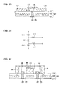
- Fig. 1F illustrates an example of the structure of a variable filter of a both-side supported lever type.
- a pair of conductive support pillars PL is formed on a dielectric substrate 20, and a lever structure movable electrode ME is formed between the support pillars.
- a transmission line L is disposed on the dielectric substrate 20 under the movable electrode ME.
- Drive electrodes DE are formed on the dielectric substrate 20 on opposite sides of the transmission line L.
- Dielectric layers 28 and 29 are formed on the transmission line L and drive electrodes DE.
- the dielectric layers 27 and 29 on the drive electrode DE may be omitted.
- the structure inside the dielectric substrate 20 is similar to that of the structure illustrated in Fig. 1C .
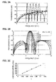
- Fig. 2A is a graph illustrating a change in the pass characteristics of a variable filter when an electric length of the transmission line is elongated by applying a DC voltage to the variable capacitors of the transmission lines L1, L2, and LC1 in the structure of Fig. 1A .
- the abscissa represents a frequency in the unit of GHz
- the ordinate represent a transmission factor in the unit of dB.
- One example illustrates the filter pass characteristics when an applied voltage is increased from 0 V to 80 V at a step of 20 V.
- the center frequency of the pass band changes from about 4.4 GHz to about 2.06 GHz.
- Fig. 2B is a graph illustrating a change in the pass band of a variable filter of the structure illustrated in Fig. 1A when a coupling coefficient k is changed.
- the coupling coefficient k becomes small from 0.1 to 0.02, the pass band width becomes narrow.
- Fig. 2C is a graph illustrating a change in a - 3 dB band width relative to a change in the coupling coefficient k.
- the - 3 dB band width is a width of a band indicating a - 3 dB change from the peak. It indicates that as the coupling coefficient k increases, the band width increases linearly.
- the center frequency and band width of the pass band are able to be controlled by changing the coupling capacitances of the transmission lines L1, L2, and LC1 of the circuit of Fig. 1A .
- a drive voltage to be applied to a drive electrode to obtain a desired center frequency and band width by using a lookup table indicating the center frequency and band width of a pass band as a function of an application voltage to obtain each coupling capacitance or capacitance value of the transmission lines L1, L2, and LC1.
- the electric length of the coupling portion transmission line LC1 is ( ⁇ /4) + x having a long physical length of the transmission line. It is preferable if a more compact structure is possible.
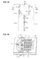
- Fig. 3A is an equivalent circuit of a variable filter of the second embodiment. Description will be made mainly on different points from the first embodiment.
- the transmission line LC1 with the open end of the first embodiment is replaced with a serial connection of a coupling portion third transmission line LC2, a variable capacitor Cc and a line VIA constituted of a via conductor. The other end of the line VIA is grounded.
- a total electric length of the coupling portion is ( ⁇ /4) + x.
- the branch portion is similar to the first embodiment, and an electric length of each resonator is ( ⁇ /4) - x.
- Fig. 3B is a perspective top view of an example of the structure realizing the circuit of Fig. 3A .
- a serial connection of a variable capacitor C1 and a transmission line L1 is connected to an input terminal IN.
- a serial connection of a variable capacitor C2 and a transmission line L2 is connected to an output terminal OUT Electrodes of a variable capacitor Cm connect the variable capacitors C1 and C2.
- the transmission lines L1 and L2 are connected to a transmission line LC2 of a coupling portion. The other end of the coupling portion transmission line is grounded via a variable capacitor Cc and a via conductor.
- a variable capacitor is formed at upper five positions of each of the transmission lines L1, L2, and LC2.
- a cross section along line A-A has, e.g., the structure of Fig. 1D .
- a cross section along line B-B has, e.g., the structure of Fig. 1C .
- the structure of the variable capacitor C1, C2 has, e.g., the structure of Fig. 1D .
- a glass epoxy substrate may be used in place of a ceramics substrate.
Landscapes
- Physics & Mathematics (AREA)
- Electromagnetism (AREA)
- Control Of Motors That Do Not Use Commutators (AREA)
Applications Claiming Priority (1)
| Application Number | Priority Date | Filing Date | Title |
|---|---|---|---|
| JP2011054681A JP2012191521A (ja) | 2011-03-11 | 2011-03-11 | 可変フィルタ装置および通信装置 |
Publications (2)
| Publication Number | Publication Date |
|---|---|
| EP2498332A1 true EP2498332A1 (fr) | 2012-09-12 |
| EP2498332B1 EP2498332B1 (fr) | 2013-10-09 |
Family
ID=45976655
Family Applications (1)
| Application Number | Title | Priority Date | Filing Date |
|---|---|---|---|
| EP20120158599 Not-in-force EP2498332B1 (fr) | 2011-03-11 | 2012-03-08 | Filtre variable et appareil de communication |
Country Status (4)
| Country | Link |
|---|---|
| US (1) | US9059497B2 (fr) |
| EP (1) | EP2498332B1 (fr) |
| JP (1) | JP2012191521A (fr) |
| CN (1) | CN102683770B (fr) |
Cited By (3)
| Publication number | Priority date | Publication date | Assignee | Title |
|---|---|---|---|---|
| EP3203640A1 (fr) | 2016-02-08 | 2017-08-09 | Bayerische Motoren Werke Aktiengesellschaft | Filtre et procédé de filtrage d'un signal d'entrée analogique à radiofréquence |
| EP3203641A1 (fr) | 2016-02-08 | 2017-08-09 | Bayerische Motoren Werke Aktiengesellschaft | Filtre et procédé permettant d'isoler des terminaux dans un circuit frontal d'un transmetteur |
| EP3975330A1 (fr) * | 2020-09-28 | 2022-03-30 | Nokia Technologies Oy | Communications radio |
Families Citing this family (4)
| Publication number | Priority date | Publication date | Assignee | Title |
|---|---|---|---|---|
| CN104854792B (zh) | 2013-10-17 | 2018-11-06 | 株式会社村田制作所 | 高频电路 |
| CN104538714B (zh) * | 2014-12-25 | 2017-04-26 | 深圳顺络电子股份有限公司 | 一种中心频率可调的带通滤波器 |
| US9590583B2 (en) | 2015-06-29 | 2017-03-07 | Agilent Technologies, Inc. | Alternating current (AC) coupler for wideband AC signals and related methods |
| EP3469395B1 (fr) * | 2016-06-14 | 2021-04-21 | Herring, Rodney | Imageur d'atmosphère terrestre radio défini par logiciel |
Citations (5)
| Publication number | Priority date | Publication date | Assignee | Title |
|---|---|---|---|---|
| WO2002041441A1 (fr) * | 2000-11-14 | 2002-05-23 | Paratek Microwave, Inc. | Filtres resonateurs hybrides a microbandes |
| US6404304B1 (en) * | 1999-10-07 | 2002-06-11 | Lg Electronics Inc. | Microwave tunable filter using microelectromechanical (MEMS) system |
| WO2008088144A1 (fr) * | 2007-01-18 | 2008-07-24 | Sung Il Kim | Dispositif accordable destiné à une application en micro-ondes/ondes millimétriques et utilisant un ruban de ligne de transmission |
| JP2008278147A (ja) | 2007-04-27 | 2008-11-13 | Fujitsu Ltd | 可変フィルタ素子、可変フィルタモジュール、およびこれらの製造方法 |
| JP2010220139A (ja) | 2009-03-19 | 2010-09-30 | Fujitsu Ltd | フィルタ、フィルタリング方法、および通信装置 |
Family Cites Families (14)
| Publication number | Priority date | Publication date | Assignee | Title |
|---|---|---|---|---|
| JPH10313226A (ja) * | 1997-05-12 | 1998-11-24 | Fujitsu Ltd | 送受分波器および送受分波器を搭載した無線通信装置 |
| JP3762109B2 (ja) * | 1998-07-31 | 2006-04-05 | 京セラ株式会社 | 配線基板の接続構造 |
| US6483406B1 (en) | 1998-07-31 | 2002-11-19 | Kyocera Corporation | High-frequency module using slot coupling |
| KR100444223B1 (ko) * | 2001-11-13 | 2004-08-16 | 삼성전기주식회사 | 유전체 세라믹 조성물 |
| JP4070116B2 (ja) * | 2003-03-24 | 2008-04-02 | 三菱電機株式会社 | 帯域可変フィルタ |
| JP4638711B2 (ja) * | 2004-10-27 | 2011-02-23 | 株式会社エヌ・ティ・ティ・ドコモ | 共振器 |
| JP4621155B2 (ja) * | 2006-02-28 | 2011-01-26 | 株式会社エヌ・ティ・ティ・ドコモ | 可変フィルタ |
| WO2008018565A1 (fr) * | 2006-08-09 | 2008-02-14 | Hitachi Metals, Ltd. | Composant à haute fréquence et circuit à haute fréquence l'utilisant |
| US20090027141A1 (en) | 2007-06-22 | 2009-01-29 | Taiyo Yuden Co., Ltd. | Filter circuit, filter circuit device, multilayered circuit board, and circuit module each including the filter circuit |
| JP4550915B2 (ja) * | 2007-06-22 | 2010-09-22 | 太陽誘電株式会社 | フィルタ回路及びフィルタ回路素子、これを備えた多層回路基板並びに回路モジュール |
| JP2009083018A (ja) * | 2007-09-28 | 2009-04-23 | Fujitsu Ltd | マイクロ構造体製造方法 |
| US7863998B2 (en) * | 2008-02-25 | 2011-01-04 | Broadcom Corporation | Method and system for processing signals via directional couplers embedded in an integrated circuit package |
| JP5375319B2 (ja) * | 2009-05-08 | 2013-12-25 | 株式会社村田製作所 | 信号線路及びその製造方法 |
| US20100295634A1 (en) * | 2009-05-20 | 2010-11-25 | Tamrat Akale | Tunable bandpass filter |
-
2011
- 2011-03-11 JP JP2011054681A patent/JP2012191521A/ja active Pending
-
2012
- 2012-03-08 EP EP20120158599 patent/EP2498332B1/fr not_active Not-in-force
- 2012-03-09 US US13/415,938 patent/US9059497B2/en not_active Expired - Fee Related
- 2012-03-09 CN CN201210061293.5A patent/CN102683770B/zh not_active Expired - Fee Related
Patent Citations (5)
| Publication number | Priority date | Publication date | Assignee | Title |
|---|---|---|---|---|
| US6404304B1 (en) * | 1999-10-07 | 2002-06-11 | Lg Electronics Inc. | Microwave tunable filter using microelectromechanical (MEMS) system |
| WO2002041441A1 (fr) * | 2000-11-14 | 2002-05-23 | Paratek Microwave, Inc. | Filtres resonateurs hybrides a microbandes |
| WO2008088144A1 (fr) * | 2007-01-18 | 2008-07-24 | Sung Il Kim | Dispositif accordable destiné à une application en micro-ondes/ondes millimétriques et utilisant un ruban de ligne de transmission |
| JP2008278147A (ja) | 2007-04-27 | 2008-11-13 | Fujitsu Ltd | 可変フィルタ素子、可変フィルタモジュール、およびこれらの製造方法 |
| JP2010220139A (ja) | 2009-03-19 | 2010-09-30 | Fujitsu Ltd | フィルタ、フィルタリング方法、および通信装置 |
Non-Patent Citations (3)
| Title |
|---|
| A. A. TAMIJANI ET AL.: "Miniature and Tunable Filters Using MEMS Capatitors", IEEE TRANS. MICROWAVE THEORY TECH., vol. 51, no. 7, July 2003 (2003-07-01), pages 1878 - 1885 |
| D. PEROULIS: "Tunable Lumped Components with Applications Reconfigurable MEMS Filters", IEEE MTT-S DIGEST, 2001, pages 341 - 344 |
| E. FOURNET: "MEMS Switchable Interdigital Coplanar Filter", IEEE TRANS. MICROWAVE THEORY TECH., vol. 51, no. 1, January 2003 (2003-01-01), pages 320 - 324 |
Cited By (6)
| Publication number | Priority date | Publication date | Assignee | Title |
|---|---|---|---|---|
| EP3203640A1 (fr) | 2016-02-08 | 2017-08-09 | Bayerische Motoren Werke Aktiengesellschaft | Filtre et procédé de filtrage d'un signal d'entrée analogique à radiofréquence |
| EP3203641A1 (fr) | 2016-02-08 | 2017-08-09 | Bayerische Motoren Werke Aktiengesellschaft | Filtre et procédé permettant d'isoler des terminaux dans un circuit frontal d'un transmetteur |
| WO2017137891A1 (fr) | 2016-02-08 | 2017-08-17 | Bayerische Motoren Werke Aktiengesellschaft | Cascade de filtres et procédé de filtrage d'un signal d'entrée analogique à radiofréquence |
| US11469791B2 (en) | 2016-02-08 | 2022-10-11 | Bayerische Motoren Werke Aktiengesellschaft | Cascade of filters and a method for filtering an analog radio-frequency input signal |
| EP3975330A1 (fr) * | 2020-09-28 | 2022-03-30 | Nokia Technologies Oy | Communications radio |
| US11888457B2 (en) | 2020-09-28 | 2024-01-30 | Nokia Technologies Oy | Radio communications |
Also Published As
| Publication number | Publication date |
|---|---|
| US9059497B2 (en) | 2015-06-16 |
| CN102683770B (zh) | 2015-04-01 |
| JP2012191521A (ja) | 2012-10-04 |
| CN102683770A (zh) | 2012-09-19 |
| US20120229231A1 (en) | 2012-09-13 |
| EP2498332B1 (fr) | 2013-10-09 |
Similar Documents
| Publication | Publication Date | Title |
|---|---|---|
| WO2013005264A1 (fr) | Dispositif de filtrage variable et dispositif de communication | |
| EP2498332B1 (fr) | Filtre variable et appareil de communication | |
| US8330562B2 (en) | Variable resonator, tunable filter, and electric circuit device | |
| JP5039162B2 (ja) | 回路素子、可変共振器、可変フィルタ | |
| US20070030100A1 (en) | LTCC based electronically tunable multilayer microstrip-stripline combline filter | |
| JP2010220139A (ja) | フィルタ、フィルタリング方法、および通信装置 | |
| Wong et al. | A new class of low-loss high-linearity electronically reconfigurable microwave filter | |
| US8643450B2 (en) | Variable distributed constant line, variable filter, and communication module | |
| US8508910B2 (en) | MEMS device | |
| JPWO2013005264A1 (ja) | 可変フィルタ装置および通信装置 | |
| US9876479B2 (en) | Filter | |
| US20040183626A1 (en) | Electronically tunable block filter with tunable transmission zeros | |
| US20050116797A1 (en) | Electronically tunable block filter | |
| WO2004073165A2 (fr) | Filtre en bloc a accord electronique presentant des zeros de transmission accordables |
Legal Events
| Date | Code | Title | Description |
|---|---|---|---|
| PUAI | Public reference made under article 153(3) epc to a published international application that has entered the european phase |
Free format text: ORIGINAL CODE: 0009012 |
|
| AK | Designated contracting states |
Kind code of ref document: A1 Designated state(s): AL AT BE BG CH CY CZ DE DK EE ES FI FR GB GR HR HU IE IS IT LI LT LU LV MC MK MT NL NO PL PT RO RS SE SI SK SM TR |
|
| AX | Request for extension of the european patent |
Extension state: BA ME |
|
| 17P | Request for examination filed |
Effective date: 20130306 |
|
| GRAP | Despatch of communication of intention to grant a patent |
Free format text: ORIGINAL CODE: EPIDOSNIGR1 |
|
| RIC1 | Information provided on ipc code assigned before grant |
Ipc: H01P 1/203 20060101AFI20130322BHEP |
|
| INTG | Intention to grant announced |
Effective date: 20130429 |
|
| GRAS | Grant fee paid |
Free format text: ORIGINAL CODE: EPIDOSNIGR3 |
|
| GRAA | (expected) grant |
Free format text: ORIGINAL CODE: 0009210 |
|
| AK | Designated contracting states |
Kind code of ref document: B1 Designated state(s): AL AT BE BG CH CY CZ DE DK EE ES FI FR GB GR HR HU IE IS IT LI LT LU LV MC MK MT NL NO PL PT RO RS SE SI SK SM TR |
|
| REG | Reference to a national code |
Ref country code: GB Ref legal event code: FG4D |
|
| REG | Reference to a national code |
Ref country code: AT Ref legal event code: REF Ref document number: 635880 Country of ref document: AT Kind code of ref document: T Effective date: 20131015 Ref country code: CH Ref legal event code: EP |
|
| REG | Reference to a national code |
Ref country code: IE Ref legal event code: FG4D |
|
| REG | Reference to a national code |
Ref country code: DE Ref legal event code: R096 Ref document number: 602012000364 Country of ref document: DE Effective date: 20131205 |
|
| REG | Reference to a national code |
Ref country code: AT Ref legal event code: MK05 Ref document number: 635880 Country of ref document: AT Kind code of ref document: T Effective date: 20131009 |
|
| REG | Reference to a national code |
Ref country code: NL Ref legal event code: VDEP Effective date: 20131009 |
|
| PG25 | Lapsed in a contracting state [announced via postgrant information from national office to epo] |
Ref country code: SI Free format text: LAPSE BECAUSE OF FAILURE TO SUBMIT A TRANSLATION OF THE DESCRIPTION OR TO PAY THE FEE WITHIN THE PRESCRIBED TIME-LIMIT Effective date: 20131009 |
|
| REG | Reference to a national code |
Ref country code: LT Ref legal event code: MG4D |
|
| PG25 | Lapsed in a contracting state [announced via postgrant information from national office to epo] |
Ref country code: SE Free format text: LAPSE BECAUSE OF FAILURE TO SUBMIT A TRANSLATION OF THE DESCRIPTION OR TO PAY THE FEE WITHIN THE PRESCRIBED TIME-LIMIT Effective date: 20131009 Ref country code: NL Free format text: LAPSE BECAUSE OF FAILURE TO SUBMIT A TRANSLATION OF THE DESCRIPTION OR TO PAY THE FEE WITHIN THE PRESCRIBED TIME-LIMIT Effective date: 20131009 Ref country code: LT Free format text: LAPSE BECAUSE OF FAILURE TO SUBMIT A TRANSLATION OF THE DESCRIPTION OR TO PAY THE FEE WITHIN THE PRESCRIBED TIME-LIMIT Effective date: 20131009 Ref country code: FI Free format text: LAPSE BECAUSE OF FAILURE TO SUBMIT A TRANSLATION OF THE DESCRIPTION OR TO PAY THE FEE WITHIN THE PRESCRIBED TIME-LIMIT Effective date: 20131009 Ref country code: BE Free format text: LAPSE BECAUSE OF FAILURE TO SUBMIT A TRANSLATION OF THE DESCRIPTION OR TO PAY THE FEE WITHIN THE PRESCRIBED TIME-LIMIT Effective date: 20131009 Ref country code: IS Free format text: LAPSE BECAUSE OF FAILURE TO SUBMIT A TRANSLATION OF THE DESCRIPTION OR TO PAY THE FEE WITHIN THE PRESCRIBED TIME-LIMIT Effective date: 20140209 Ref country code: HR Free format text: LAPSE BECAUSE OF FAILURE TO SUBMIT A TRANSLATION OF THE DESCRIPTION OR TO PAY THE FEE WITHIN THE PRESCRIBED TIME-LIMIT Effective date: 20131009 Ref country code: NO Free format text: LAPSE BECAUSE OF FAILURE TO SUBMIT A TRANSLATION OF THE DESCRIPTION OR TO PAY THE FEE WITHIN THE PRESCRIBED TIME-LIMIT Effective date: 20140109 |
|
| PG25 | Lapsed in a contracting state [announced via postgrant information from national office to epo] |
Ref country code: PL Free format text: LAPSE BECAUSE OF FAILURE TO SUBMIT A TRANSLATION OF THE DESCRIPTION OR TO PAY THE FEE WITHIN THE PRESCRIBED TIME-LIMIT Effective date: 20131009 Ref country code: CY Free format text: LAPSE BECAUSE OF FAILURE TO SUBMIT A TRANSLATION OF THE DESCRIPTION OR TO PAY THE FEE WITHIN THE PRESCRIBED TIME-LIMIT Effective date: 20131009 Ref country code: LV Free format text: LAPSE BECAUSE OF FAILURE TO SUBMIT A TRANSLATION OF THE DESCRIPTION OR TO PAY THE FEE WITHIN THE PRESCRIBED TIME-LIMIT Effective date: 20131009 Ref country code: RS Free format text: LAPSE BECAUSE OF FAILURE TO SUBMIT A TRANSLATION OF THE DESCRIPTION OR TO PAY THE FEE WITHIN THE PRESCRIBED TIME-LIMIT Effective date: 20131009 Ref country code: AT Free format text: LAPSE BECAUSE OF FAILURE TO SUBMIT A TRANSLATION OF THE DESCRIPTION OR TO PAY THE FEE WITHIN THE PRESCRIBED TIME-LIMIT Effective date: 20131009 Ref country code: ES Free format text: LAPSE BECAUSE OF FAILURE TO SUBMIT A TRANSLATION OF THE DESCRIPTION OR TO PAY THE FEE WITHIN THE PRESCRIBED TIME-LIMIT Effective date: 20131009 |
|
| PG25 | Lapsed in a contracting state [announced via postgrant information from national office to epo] |
Ref country code: PT Free format text: LAPSE BECAUSE OF FAILURE TO SUBMIT A TRANSLATION OF THE DESCRIPTION OR TO PAY THE FEE WITHIN THE PRESCRIBED TIME-LIMIT Effective date: 20140210 |
|
| REG | Reference to a national code |
Ref country code: DE Ref legal event code: R097 Ref document number: 602012000364 Country of ref document: DE |
|
| PG25 | Lapsed in a contracting state [announced via postgrant information from national office to epo] |
Ref country code: EE Free format text: LAPSE BECAUSE OF FAILURE TO SUBMIT A TRANSLATION OF THE DESCRIPTION OR TO PAY THE FEE WITHIN THE PRESCRIBED TIME-LIMIT Effective date: 20131009 |
|
| PLBE | No opposition filed within time limit |
Free format text: ORIGINAL CODE: 0009261 |
|
| STAA | Information on the status of an ep patent application or granted ep patent |
Free format text: STATUS: NO OPPOSITION FILED WITHIN TIME LIMIT |
|
| PG25 | Lapsed in a contracting state [announced via postgrant information from national office to epo] |
Ref country code: IT Free format text: LAPSE BECAUSE OF FAILURE TO SUBMIT A TRANSLATION OF THE DESCRIPTION OR TO PAY THE FEE WITHIN THE PRESCRIBED TIME-LIMIT Effective date: 20131009 Ref country code: SK Free format text: LAPSE BECAUSE OF FAILURE TO SUBMIT A TRANSLATION OF THE DESCRIPTION OR TO PAY THE FEE WITHIN THE PRESCRIBED TIME-LIMIT Effective date: 20131009 Ref country code: CZ Free format text: LAPSE BECAUSE OF FAILURE TO SUBMIT A TRANSLATION OF THE DESCRIPTION OR TO PAY THE FEE WITHIN THE PRESCRIBED TIME-LIMIT Effective date: 20131009 Ref country code: RO Free format text: LAPSE BECAUSE OF FAILURE TO SUBMIT A TRANSLATION OF THE DESCRIPTION OR TO PAY THE FEE WITHIN THE PRESCRIBED TIME-LIMIT Effective date: 20131009 |
|
| 26N | No opposition filed |
Effective date: 20140710 |
|
| PG25 | Lapsed in a contracting state [announced via postgrant information from national office to epo] |
Ref country code: DK Free format text: LAPSE BECAUSE OF FAILURE TO SUBMIT A TRANSLATION OF THE DESCRIPTION OR TO PAY THE FEE WITHIN THE PRESCRIBED TIME-LIMIT Effective date: 20131009 |
|
| REG | Reference to a national code |
Ref country code: DE Ref legal event code: R097 Ref document number: 602012000364 Country of ref document: DE Effective date: 20140710 |
|
| PG25 | Lapsed in a contracting state [announced via postgrant information from national office to epo] |
Ref country code: LU Free format text: LAPSE BECAUSE OF FAILURE TO SUBMIT A TRANSLATION OF THE DESCRIPTION OR TO PAY THE FEE WITHIN THE PRESCRIBED TIME-LIMIT Effective date: 20140308 |
|
| REG | Reference to a national code |
Ref country code: IE Ref legal event code: MM4A |
|
| PG25 | Lapsed in a contracting state [announced via postgrant information from national office to epo] |
Ref country code: IE Free format text: LAPSE BECAUSE OF NON-PAYMENT OF DUE FEES Effective date: 20140308 |
|
| REG | Reference to a national code |
Ref country code: CH Ref legal event code: PL |
|
| PG25 | Lapsed in a contracting state [announced via postgrant information from national office to epo] |
Ref country code: CH Free format text: LAPSE BECAUSE OF NON-PAYMENT OF DUE FEES Effective date: 20150331 Ref country code: LI Free format text: LAPSE BECAUSE OF NON-PAYMENT OF DUE FEES Effective date: 20150331 |
|
| REG | Reference to a national code |
Ref country code: FR Ref legal event code: PLFP Year of fee payment: 5 |
|
| PG25 | Lapsed in a contracting state [announced via postgrant information from national office to epo] |
Ref country code: MT Free format text: LAPSE BECAUSE OF FAILURE TO SUBMIT A TRANSLATION OF THE DESCRIPTION OR TO PAY THE FEE WITHIN THE PRESCRIBED TIME-LIMIT Effective date: 20131009 |
|
| PG25 | Lapsed in a contracting state [announced via postgrant information from national office to epo] |
Ref country code: SM Free format text: LAPSE BECAUSE OF FAILURE TO SUBMIT A TRANSLATION OF THE DESCRIPTION OR TO PAY THE FEE WITHIN THE PRESCRIBED TIME-LIMIT Effective date: 20131009 |
|
| PG25 | Lapsed in a contracting state [announced via postgrant information from national office to epo] |
Ref country code: MC Free format text: LAPSE BECAUSE OF FAILURE TO SUBMIT A TRANSLATION OF THE DESCRIPTION OR TO PAY THE FEE WITHIN THE PRESCRIBED TIME-LIMIT Effective date: 20131009 |
|
| PG25 | Lapsed in a contracting state [announced via postgrant information from national office to epo] |
Ref country code: BG Free format text: LAPSE BECAUSE OF FAILURE TO SUBMIT A TRANSLATION OF THE DESCRIPTION OR TO PAY THE FEE WITHIN THE PRESCRIBED TIME-LIMIT Effective date: 20131009 Ref country code: GR Free format text: LAPSE BECAUSE OF FAILURE TO SUBMIT A TRANSLATION OF THE DESCRIPTION OR TO PAY THE FEE WITHIN THE PRESCRIBED TIME-LIMIT Effective date: 20140110 |
|
| PG25 | Lapsed in a contracting state [announced via postgrant information from national office to epo] |
Ref country code: TR Free format text: LAPSE BECAUSE OF FAILURE TO SUBMIT A TRANSLATION OF THE DESCRIPTION OR TO PAY THE FEE WITHIN THE PRESCRIBED TIME-LIMIT Effective date: 20131009 Ref country code: HU Free format text: LAPSE BECAUSE OF FAILURE TO SUBMIT A TRANSLATION OF THE DESCRIPTION OR TO PAY THE FEE WITHIN THE PRESCRIBED TIME-LIMIT; INVALID AB INITIO Effective date: 20120308 |
|
| REG | Reference to a national code |
Ref country code: FR Ref legal event code: PLFP Year of fee payment: 6 |
|
| PGFP | Annual fee paid to national office [announced via postgrant information from national office to epo] |
Ref country code: DE Payment date: 20170228 Year of fee payment: 6 Ref country code: FR Payment date: 20170213 Year of fee payment: 6 |
|
| PGFP | Annual fee paid to national office [announced via postgrant information from national office to epo] |
Ref country code: GB Payment date: 20170308 Year of fee payment: 6 |
|
| PG25 | Lapsed in a contracting state [announced via postgrant information from national office to epo] |
Ref country code: MK Free format text: LAPSE BECAUSE OF FAILURE TO SUBMIT A TRANSLATION OF THE DESCRIPTION OR TO PAY THE FEE WITHIN THE PRESCRIBED TIME-LIMIT Effective date: 20131009 |
|
| REG | Reference to a national code |
Ref country code: DE Ref legal event code: R119 Ref document number: 602012000364 Country of ref document: DE |
|
| PG25 | Lapsed in a contracting state [announced via postgrant information from national office to epo] |
Ref country code: AL Free format text: LAPSE BECAUSE OF FAILURE TO SUBMIT A TRANSLATION OF THE DESCRIPTION OR TO PAY THE FEE WITHIN THE PRESCRIBED TIME-LIMIT Effective date: 20131009 |
|
| GBPC | Gb: european patent ceased through non-payment of renewal fee |
Effective date: 20180308 |
|
| PG25 | Lapsed in a contracting state [announced via postgrant information from national office to epo] |
Ref country code: DE Free format text: LAPSE BECAUSE OF NON-PAYMENT OF DUE FEES Effective date: 20181002 |
|
| PG25 | Lapsed in a contracting state [announced via postgrant information from national office to epo] |
Ref country code: GB Free format text: LAPSE BECAUSE OF NON-PAYMENT OF DUE FEES Effective date: 20180308 |
|
| PG25 | Lapsed in a contracting state [announced via postgrant information from national office to epo] |
Ref country code: FR Free format text: LAPSE BECAUSE OF NON-PAYMENT OF DUE FEES Effective date: 20180331 |