US9876479B2 - Filter - Google Patents
Filter Download PDFInfo
- Publication number
- US9876479B2 US9876479B2 US15/150,882 US201615150882A US9876479B2 US 9876479 B2 US9876479 B2 US 9876479B2 US 201615150882 A US201615150882 A US 201615150882A US 9876479 B2 US9876479 B2 US 9876479B2
- Authority
- US
- United States
- Prior art keywords
- filter
- signal line
- resonant lines
- resonant
- line
- Prior art date
- Legal status (The legal status is an assumption and is not a legal conclusion. Google has not performed a legal analysis and makes no representation as to the accuracy of the status listed.)
- Active, expires
Links
Images


Classifications
-
- H—ELECTRICITY
- H03—ELECTRONIC CIRCUITRY
- H03H—IMPEDANCE NETWORKS, e.g. RESONANT CIRCUITS; RESONATORS
- H03H7/00—Multiple-port networks comprising only passive electrical elements as network components
- H03H7/01—Frequency selective two-port networks
- H03H7/12—Bandpass or bandstop filters with adjustable bandwidth and fixed centre frequency
-
- H—ELECTRICITY
- H03—ELECTRONIC CIRCUITRY
- H03H—IMPEDANCE NETWORKS, e.g. RESONANT CIRCUITS; RESONATORS
- H03H7/00—Multiple-port networks comprising only passive electrical elements as network components
- H03H7/01—Frequency selective two-port networks
- H03H7/0123—Frequency selective two-port networks comprising distributed impedance elements together with lumped impedance elements
-
- H—ELECTRICITY
- H01—ELECTRIC ELEMENTS
- H01P—WAVEGUIDES; RESONATORS, LINES, OR OTHER DEVICES OF THE WAVEGUIDE TYPE
- H01P1/00—Auxiliary devices
- H01P1/20—Frequency-selective devices, e.g. filters
- H01P1/201—Filters for transverse electromagnetic waves
- H01P1/203—Strip line filters
-
- H—ELECTRICITY
- H01—ELECTRIC ELEMENTS
- H01P—WAVEGUIDES; RESONATORS, LINES, OR OTHER DEVICES OF THE WAVEGUIDE TYPE
- H01P1/00—Auxiliary devices
- H01P1/20—Frequency-selective devices, e.g. filters
- H01P1/213—Frequency-selective devices, e.g. filters combining or separating two or more different frequencies
- H01P1/2135—Frequency-selective devices, e.g. filters combining or separating two or more different frequencies using strip line filters
-
- H—ELECTRICITY
- H01—ELECTRIC ELEMENTS
- H01P—WAVEGUIDES; RESONATORS, LINES, OR OTHER DEVICES OF THE WAVEGUIDE TYPE
- H01P1/00—Auxiliary devices
- H01P1/20—Frequency-selective devices, e.g. filters
- H01P1/213—Frequency-selective devices, e.g. filters combining or separating two or more different frequencies
- H01P1/2136—Frequency-selective devices, e.g. filters combining or separating two or more different frequencies using comb or interdigital filters; using cascaded coaxial cavities
-
- H—ELECTRICITY
- H01—ELECTRIC ELEMENTS
- H01P—WAVEGUIDES; RESONATORS, LINES, OR OTHER DEVICES OF THE WAVEGUIDE TYPE
- H01P3/00—Waveguides; Transmission lines of the waveguide type
- H01P3/02—Waveguides; Transmission lines of the waveguide type with two longitudinal conductors
- H01P3/08—Microstrips; Strip lines
- H01P3/081—Microstriplines
- H01P3/082—Multilayer dielectric
-
- H—ELECTRICITY
- H03—ELECTRONIC CIRCUITRY
- H03H—IMPEDANCE NETWORKS, e.g. RESONANT CIRCUITS; RESONATORS
- H03H7/00—Multiple-port networks comprising only passive electrical elements as network components
- H03H7/01—Frequency selective two-port networks
-
- H—ELECTRICITY
- H03—ELECTRONIC CIRCUITRY
- H03H—IMPEDANCE NETWORKS, e.g. RESONANT CIRCUITS; RESONATORS
- H03H7/00—Multiple-port networks comprising only passive electrical elements as network components
- H03H7/01—Frequency selective two-port networks
- H03H7/0153—Electrical filters; Controlling thereof
-
- H—ELECTRICITY
- H03—ELECTRONIC CIRCUITRY
- H03H—IMPEDANCE NETWORKS, e.g. RESONANT CIRCUITS; RESONATORS
- H03H7/00—Multiple-port networks comprising only passive electrical elements as network components
- H03H7/01—Frequency selective two-port networks
- H03H7/09—Filters comprising mutual inductance
-
- H—ELECTRICITY
- H01—ELECTRIC ELEMENTS
- H01P—WAVEGUIDES; RESONATORS, LINES, OR OTHER DEVICES OF THE WAVEGUIDE TYPE
- H01P1/00—Auxiliary devices
- H01P1/20—Frequency-selective devices, e.g. filters
- H01P1/201—Filters for transverse electromagnetic waves
- H01P1/203—Strip line filters
- H01P1/20327—Electromagnetic interstage coupling
- H01P1/20354—Non-comb or non-interdigital filters
- H01P1/20381—Special shape resonators
Definitions
- the embodiment discussed herein is related to a filter which allows a predetermined frequency band signal to pass through.
- FIG. 1 is a circuit diagram illustrating a configuration of a related high frequency variable filter.
- the high frequency variable filter illustrated in FIG. 1 includes a plurality of channel filters 101 a to 101 c , and switches 102 a and 102 b .
- the passbands of the channel filters 101 a to 101 c differ from one another.
- a high frequency signal input from an input terminal 103 is output from an output terminal 104 via one channel filter selected by the switches 102 a and 102 b .
- By switching the switches 102 a and 102 b it is possible to change the passband of the high frequency variable filter.
- JP-A 10-335903 and JP-A 2007-174438 disclose the heretofore described kind of high frequency variable filter including the plurality of channel filters and the switches.
- the configuration illustrated in FIG. 1 includes a number of filters equivalent to the number of channels. For this reason, as well as the size of the high frequency variable filter increasing, a cost also increases. Also, a loss of signal occurs in each switch.
- An MEMS device such as an MEMS switch may be applied to a high frequency band variable filter with a high Q (quality factor).
- the MEMS device because of its small size and low loss, is often used in a CPW distributed constant resonator (CPW: Coplanar Waveguide).
- CPW distributed constant resonator
- quartz and glass are used as substrate materials.
- the drive electrodes of the variable capacitors are disposed in a gap between a ground line and signal line formed on a substrate. Also, the length of the lines is defined by the permittivity of the substrate.
- the lower the frequency band the larger the size.
- the usable frequency band of principal mobile communication equipment such as a portable telephone is approximately 800 MHz to 6 GHz.
- the size of the distributed constant filter is too large for practical use.
- a filter includes a substrate, a signal line formed on the substrate, including an input terminal and an output terminal at either end of the signal line, and a first pair of resonant lines connected between the signal line and a ground portion, wherein the first pair of resonant lines are connected to the signal line at the same point.
- FIG. 1 is a circuit diagram of a configuration of a related filter
- FIG. 2 is a circuit diagram of a filter in the embodiment
- FIG. 3 is a circuit diagram of a configuration of a filter in which a coupling circuit is connected
- FIGS. 4A to 4N are circuit diagrams of the coupling circuit
- FIG. 5 is a circuit diagram illustrating another configuration of the filter
- FIG. 6A is a plan view of a configuration wherein resonant lines are connected to a common ground;
- FIG. 6B is a plan view of a configuration wherein resonant lines are formed into an arc shape
- FIG. 7A is a plan view of a resonant line of a variable filter element taken along the line A-A in FIG. 6B ;
- FIG. 7B is a sectional view taken along Z-Z in FIG. 7A ;
- FIGS. 8A to 8G are sectional views illustrating a process of manufacturing the variable filter element
- FIG. 9 is a block diagram of a configuration of a communication module
- FIG. 10 is a block diagram of a configuration of a communication module including variable filters
- FIG. 11 is a block diagram of a configuration of a communication apparatus.
- FIG. 12 is a block diagram of a configuration of a communication apparatus including variable filters.
- the input line 2 a , resonant lines 2 b and 2 c , and output line 2 d are formed by a distributed constant transmission line.
- two resonant lines connected in parallel at the same point are defined as a “pair of resonant lines”.
- the input-output impedance of the filter illustrated in FIG. 2 is taken to be, for example, 50 ⁇ . Also, the impedance of the resonant lines 2 b and 2 c , being lower than at least the impedance of the input line 2 a and output line 2 d , is taken to be, in the embodiment, 20 ⁇ as an example.
- ⁇ is a wavelength (a resonant wavelength), in the distributed constant transmission line, of the frequency (the resonant frequency of the resonant lines 2 b and 2 c ) of a signal extracted in the filter of the embodiment.
- each of the resonant lines 2 b and 2 c means a resonator of which one end is connected to ground, and which is formed by the distributed constant transmission line.
- each of the resonant lines 2 b and 2 c By connecting one end of each of the resonant lines 2 b and 2 c to ground in this way, signals input into the resonant lines 2 b and 2 c via the input line 2 a are filtered by being totally reflected from the ground ends of the resonant lines 2 b and 2 c , enabling a desired frequency signal to be extracted from the output terminal 4 .
- the pair of resonant lines 2 b and 2 c are disposed in positions facing each other across the signal line connecting the input terminal 1 and output terminal 4 . Because of this, it is possible to dispose the resonant lines in high density, so it is possible to further reduce the size of the filter in the signal line direction. Even in the event that the resonant lines are disposed on the same side (one side) with respect to the signal line, it is possible to reduce the size of the filter in the signal line direction.
- an output line 12 g is connected between a contact point 13 b and output terminal 4 .
- a resonant line 12 e and resonant line 12 f are connected between the contact point 13 b and ground. That is, the resonant lines 12 e and 12 f are connected in parallel to the contact point 13 b . Also, the resonant lines 12 e and 12 f are connected to the same position (the contact point 13 b ) in the signal line.
- a description has been given of an example in which the resonant lines 12 b , 12 c , 12 e , and 12 f are connected to ground, but it is also acceptable that they have an open end.
- a coupling circuit 14 is connected between the contact point 13 a and contact point 13 b .
- the coupling circuit 14 is a circuit which couples the contact point 13 a and contact point 13 b in the filter.
- the coupling circuit 14 may be realized by, for example, a capacitor connected in series between the contact point 13 a and contact point 13 b.
- the signals input into the input terminal 1 are input into the resonant lines 12 b and 12 c via the input line 12 a .
- a signal which meets a resonant condition of the resonant lines 12 b and 12 c is totally reflected from the ground ends of the resonant lines 12 b and 12 c , but a signal which does not meet the resonant condition, by being grounded, or reflected to the input end side, is attenuated (a filtering).
- the coupling circuit 14 may be realized by only the capacitor, as heretofore described, but various other forms are also conceivable.
- the coupling circuit illustrated in FIG. 4B is an example of a ⁇ type coupling circuit.
- the input side and output side are connected by a circuit block 141 , and both ends of the circuit block 141 , and ground, are connected by circuit blocks 142 and 143 .
- the coupling circuit illustrated in FIG. 4D includes a capacitor C 1 connected to the signal line connecting the input terminal and output terminal, and two inductors L 1 and L 2 connected between the signal line and ground.
- the coupling circuit illustrated in FIG. 4E illustrates a circuit in which the circuit block 141 includes a plurality of elements.
- This coupling circuit includes two distributed constant elements 14 b and 14 c , and a capacitor C 11 , which are connected in series to the signal line, and two inductors L 11 and L 12 connected between the signal line and ground.
- the coupling circuit illustrated in FIG. 4G illustrates a circuit in which each of the circuit blocks 141 to 143 includes combining an inductor and capacitor connected in parallel.
- This coupling circuit is a circuit in which a combination of an inductor L 31 and capacitor C 31 connected in parallel is connected to the signal line, and a combination of an inductor L 32 and capacitor C 32 connected in parallel, and a combination of an inductor L 33 and capacitor C 33 connected in parallel, are connected between the signal line and ground.
- the coupling circuit illustrated in FIG. 4I is a circuit in which a distributed constant element 14 e is connected to the signal line, and a combination of an inductor L 51 and capacitor C 51 connected in parallel, and a combination of an inductor L 52 and capacitor C 52 connected in parallel, are connected between the signal line and ground.
- the coupling circuit illustrated in FIG. 4L is a circuit in which an inductor L 71 and a combination of an inductor L 72 and capacitor C 71 connected in parallel are connected to the signal line, and a combination of an inductor L 73 and capacitor C 72 connected in parallel, and a combination of an inductor L 74 and capacitor C 73 connected in parallel, are connected between the signal line and ground.
- FIGS. 4M and 4N are examples of the T type coupling circuit.
- FIG. 4M illustrates a circuit in which a combination of a capacitor C 91 and inductor L 91 connected in parallel, and a combination of a capacitor C 92 and inductor L 92 connected in parallel, are connected in series to the signal line connecting the input terminal and output terminal, and a combination of a capacitor C 93 and inductor L 93 connected in parallel is connected between the signal line and ground.
- the coupling circuit illustrated in FIG. 4N is a circuit which includes distributed constant elements 14 f and 14 g connected in series to the signal line, and a distributed constant element 14 h connected between the signal line and ground.
- the ⁇ type coupling circuit having two contact points on the signal line connected between the input terminal and output terminal, a lumped constant element or distributed constant element is connected between each contact point and the ground. It is preferable that the elements connected between the contact points and ground have a symmetry. For example, it is preferable that the same element is installed in an a 1 section and a 2 section in FIG. 4D . In the event of a configuration wherein the same element is installed in the a 1 section and a 2 section, it is acceptable to install inductors, as illustrated in FIG. 4D or the like, it is acceptable to install capacitors, as illustrated in FIG. 4H , and it is acceptable to install a plurality of lumped constant elements, as illustrated in FIG. 4G or the like.
- the resonant lines 12 b and 12 c function in combination as one resonator.
- the resonated signal after being resonated again in the same way as heretofore described in the resonant lines 12 e and 12 f , via the coupling circuit 14 , is output from the output terminal 4 via the output line 12 g .
- the filter performs its function.
- the pair of resonant lines on the input side and the pair of resonant lines on the output side are connected by the one coupling circuit 14 .
- the number of pairs of resonant lines included in the filter not being limited to two, it is possible to connect three or a larger number.
- a connecting of a much larger number of paired resonant lines may be realized by connecting them by means of a coupling circuit which couples a signal between one pair of resonant lines and another pair of resonant lines, and repeating this kind of connection structure.
- the number of resonators included in the whole of the filter increasing, it is possible to realize a filter with a good steepness.
- FIG. 5 is a circuit diagram illustrating another configuration example of a filter.
- an input line 22 a is connected between an input terminal 1 and a contact point 23 a .
- a resonant line 22 b is connected between the contact point 23 a and ground.
- a first coupling circuit 24 is connected between the contact point 23 a and a contact point 23 b .
- a resonant line 22 c and resonant line 22 d are connected between the contact point 23 b and ground.
- a second coupling circuit 25 is connected between the contact point 23 b and a contact point 23 c .
- a resonant line 22 e is connected between the contact point 23 c and ground.
- An output line 22 f is connected between the contact point 23 c and an output terminal 4 .
- first coupling circuit 24 and second coupling circuit 25 it is possible to use the ⁇ type coupling circuit or T type coupling circuit.
- ⁇ type coupling circuit or T type coupling circuit it is possible to employ one of the coupling circuits illustrated in FIGS. 4A to 4N .
- a coupling circuit which is connected in the ⁇ type or T type includes a lumped constant element, as illustrated in FIGS. 4E, 4F, and 41 , it is possible to connect a distributed constant element to one portion.
- the input side line and output side line are connected by the first coupling circuit 24 and second coupling circuit 25 but, by increasing the number of coupling circuits, it is possible to connect still more paired resonant lines connected between the signal line and ground.
- ground ends of the resonant lines 12 b , 12 c , 12 e , and 12 f illustrated in FIGS. 3 and 5 are connected one to each independent ground, and it is also acceptable that they are connected to an identical ground.
- FIG. 6A is a plan view illustrating a specific configuration of a filter.
- the circuit illustrated in FIG. 4F is employed as the coupling circuit 14 .
- components identical to the components illustrated in FIGS. 3 and 4F are given identical reference numerals and characters.
- resonant lines 12 b ′, 12 c ′, 12 e ′, and 12 f ′ connected one to each independent ground are depicted by the broken lines, while resonant lines 12 b , 12 c , 12 e , and 12 f connected to an identical ground are depicted by the solid lines.
- the line lengths of the resonant lines 12 b , 12 c , 12 e , 12 f , 12 b ′, 12 c ′, 12 e ′, and 12 f ′ are all taken to be W 1 .
- the resonant lines 12 b , 12 c , 12 e , and 12 f , and a distributed constant element 14 d are each constructed in such a way that a plurality of capacitor electrodes straddle a signal line (a description of the capacitor electrodes will be given hereafter).
- the resonant lines 12 b and 12 e are connected to an identical ground G 1 .
- the resonant lines 12 c and 12 f are connected to an identical ground G 2 .
- the resonant line 12 b ′ is connected to a ground G 1 ′.
- the resonant line 12 c ′ is connected to a ground G 2 ′.
- the resonant line 12 e ′ is connected to a ground G 3 ′.
- the resonant line 12 f ′ is connected to a ground G 4 ′.
- the grounds G 1 ′ to G 4 ′ are physically independent of one another.
- a space for disposing the resonant lines 12 b and 12 e is of a dimension W 3 (W 3 ⁇ W 2 ) in the direction perpendicular to the signal line.
- FIG. 6B illustrates another example of a filter in which resonant lines are connected to an identical ground.
- the filter illustrated in FIG. 6B differs from the filter illustrated in FIG. 6A in that the resonant lines 12 b , 12 c , 12 e , and 12 f are formed into an arc shape.
- a line length W 11 of each resonant line 12 b , 12 c , 12 e , and 12 f is the same as the line length W 1 of the resonant lines illustrated in FIG. 6A .
- a loss of the filter basically depends on a line conductor loss.
- the filter according to the embodiment may be used as, for example, a small GHz band frequency variable filter using an MEMS variable capacitor.
- variable filter which may vary the passband.
- the movable capacitor electrode By mounting the movable capacitor electrode on the resonant lines, it is possible to shorten the line length and, as well as it being possible to further miniaturize the filter, it is possible to vary the passband.
- the movable capacitor electrode By mounting the movable capacitor electrode on the coupling circuit, it is possible to equivalently change the electrical length of the resonator in such a way as to provide a coupling circuit in accordance with the passband varied in the resonant lines.
- variable filters have the variable capacitors, but it is also acceptable to realize them with variable inductors. Furthermore, it is acceptable to realize the variable filters by appropriately combining the variable capacitors and variable inductors.
- a coupling circuit including only lumped constant elements is installed in the variable filter, as illustrated in FIGS. 4D, 4G, 4H, 4J, 4K, 4L, and 4M , it is sufficient to change at least one lumped constant element, among the lumped constant elements included in the coupling circuit, to a variable element.
- the coupling circuit illustrated in FIG. 4D is installed, by changing the capacitor C 1 to a variable capacitor, it is possible to realize the coupling circuit in accordance with the passband.
- a coupling circuit including a plurality of distributed constant elements is installed in the filter, as illustrated in FIG. 4N , by installing a movable capacitor electrode as at least one distributed constant element, among the distributed constant elements 14 f , 14 g , and 14 h included in the coupling circuit, it is possible to realize the variable filter.
- variable capacitor electrode in the resonant lines, as in the embodiment, it being possible to change the capacitance in the resonant lines, it is possible to change a signal passband in the resonant lines.
- the resonant lines, in which the passband is variable in the filter in this way, it is possible to realize the variable filter.
- variable capacitor element a specific configuration of the resonant lines including the movable capacitor electrode (hereafter referred to as the variable capacitor element).
- FIG. 7A is a plan view of the variable capacitor element.
- FIG. 7B is a sectional view of a Z-Z section in FIG. 7A .
- variable capacitor element illustrated in FIGS. 7A and 7B including a substrate 31 , a signal line 32 , movable capacitor electrodes 33 , drive electrodes 35 a and 35 b , a dielectric dot 36 , anchor sections 37 a and 37 b , electrode pads 38 , and a packaging member 39 , is configured as one portion of a filter which allows a passage of an electromagnetic wave or electrical signal in a specified high frequency band.
- the packaging member 39 seals not only a variable capacitor element section, but the whole of the filter.
- the substrate 31 is an LTCC wafer (LTCC: Low Temperature Co-fired Ceramics) including multilayer internal wirings (wiring patterns 31 c ).
- the substrate 31 is formed by mutually bonding a plurality (five in the substrate illustrated in FIG. 7B ) of insulating layers 31 a .
- a via 31 b which includes a conductive portion in a through hole formed from one principal surface to the other principal surface is formed in each insulating layer 31 a .
- each wiring pattern 31 c is sandwiched between at least one pair of adjacent insulating layers 31 a .
- one portion of the wiring pattern 31 c positioned on a side of the substrate 31 closest to a first surface 31 e is a ground line 31 d connected to ground.
- the ground line 31 d faces the signal line 32 across the insulating layer 31 a , and the ground line 31 d and signal line 32 have a gap CG 2 between them.
- the ground line 31 d illustrated in FIG. 7B an example has been described in which it is disposed in a position close to the first surface but, it not being limited to this, it is also acceptable to dispose it on another layer.
- the ground line 31 d faces the signal line 32 across a plurality of the insulating layers 31 a .
- the gap CG 2 between the ground line 31 d and signal line 32 is equivalent to a thickness to which the plurality of insulating layers 31 a are stacked.
- the wiring patterns 31 c are connected, and the wiring patterns 31 c and electrode pads 38 are connected, by the vias 31 b . In some cases, it is acceptable that the wiring patterns 31 c and signal line 32 are connected by the vias 31 b .
- the insulating layers 31 a are realized by an LTCC. However, their not being limited to the LTCC, it is acceptable to form them from another dielectric body.
- the signal line 32 is a conductor pattern in which an electrical signal passes between the terminals 32 a and 32 b .
- the terminals 32 a and 32 b by being connected to other elements on the wiring substrate, or made an open end, are electrically connected to predetermined electrode pads 38 via predetermined vias 31 b and wiring patterns 31 c in the wiring substrate 31 (not illustrated).
- the signal line 32 being a distributed constant transmission line of which the impedance is, for example, 20 ⁇ , is formed from a low resistance metal material such as, for example, Cu, Ag, Au, Al, W, or Mo.
- the thickness of the signal line 32 is, for example, 0.5 to 20 ⁇ m.
- each movable capacitor electrode 33 Both ends of each movable capacitor electrode 33 are fixed to the anchor sections 37 a and 37 b formed on the first surface 31 e of the substrate 31 , and a main portion thereof excluding both ends faces the signal line 32 and drive electrodes 35 a and 35 b across an air gap.
- a thick section 33 a is formed in a portion of each movable capacitor electrode 33 facing the signal line 32 .
- the thick sections 33 a and signal line 32 face each other across a gap CG 1 .
- the movable capacitor electrodes 33 are connected to ground via the anchor sections 37 a and 37 b , vias 31 b , and wiring patterns 31 c .
- the movable capacitor electrodes 33 being formed from an elastically deformable material, may be formed from, for example, a low resistance metal such as, for example, Au, Cu, or Al.
- the variable capacitor element whose capacitance changes is realized by the movable capacitor electrodes 33 being moved to change a distance between the movable capacitor electrodes 33 and signal line 32 .
- the gap CG 1 between the movable capacitor electrodes 33 and signal line 32 may be made, for example, 0.1 to 10 ⁇ m.
- the movable capacitor electrodes 33 and ground line 31 d are one example of a ground wiring section in the embodiment.
- the drive electrodes 35 a and 35 b being disposed adjacent to the signal line 32 , face one portion of each movable capacitor electrode 33 .
- the drive electrodes 35 a and 35 b generate an electrostatic attractive force between themselves and the movable capacitor electrodes 33 , enabling the movable capacitor electrodes 33 to be displaced in a direction indicated by an arrow A.
- the drive electrodes 35 a and 35 b are formed from a high resistance metal thin film such as, for example, a SiCr thin film.
- a gap between the drive electrodes 35 a and 35 b and movable capacitor electrodes 33 is made equal to or more than three times the gap CG 1 between the movable capacitor electrodes 33 and signal line 32 .
- the dielectric dot 36 being provided on the signal line 32 , is formed from a dielectric material such as, for example, Al2O3, SiO2, SixNy, or SiOC.
- the dielectric dot 36 may increase a capacitance occurring in the gap CG 1 between the signal line 32 and movable capacitor electrodes 33 . It is preferable to increase the capacitance because it is thereby possible to ensure a wide filter frequency variable range.
- the packaging member 39 seals structures of the filter which, being bonded to the first surface 31 e of the substrate 31 , are formed on the first surface 31 e of the substrate 31 .
- a first capacitor is formed by the gap CG 2 being formed between the signal line 32 and the ground line 31 d disposed in the substrate 31 .
- a second capacitor is formed by the gap CG 1 being formed between the signal line 32 and movable capacitor electrodes 33 .
- the drive electrodes 35 a and 35 b are configured so that a voltage may be applied to each individual one. Then, by selectively applying a voltage to the divided drive electrodes 35 a and 35 b , the plurality of movable capacitor electrodes 33 are selectively displaced. The movable capacitor electrodes 33 are selectively displaced, thereby enabling changes in capacitance to differ in magnitude.
- variable filter by installing this kind of variable capacitor element in, for example, the resonant lines 12 b , 12 c , 12 e , and 12 f , and coupling circuit 14 illustrated in FIG. 3 , or the resonant lines 22 b , 22 c , 22 d , and 22 e , and coupling circuit 24 illustrated in FIG. 5 .
- a signal line one being an example
- ground lines for example, two
- there is a limitation on a drive electrode disposition space there is a limit to increasing the area of the drive electrode.
- the variable filter element using the microstrip line illustrated in FIGS. 7A and 7B has no ground line provided on a surface of the substrate the same as the surface on which the signal line is formed, it is possible to secure a large area of the drive electrodes 35 a and 35 b on the substrate 31 .
- FIGS. 8A to 8G are sectional views illustrating a process of manufacturing the variable filter element.
- the electrode pads 38 are formed on a second surface 31 f of the substrate 31 including the multilayer internal wirings.
- the electrode pads 38 may be formed by, for example, after forming a predetermined metal material as a film on the second surface 31 f of the substrate 31 by means of a sputtering method, patterning the metal film by means of a predetermined wet etching or dry etching. Alternatively, in the formation of the electrode pads 38 , it is possible to employ a nonelectrolytic plating method or electroplating method.
- the drive electrodes 35 a and 35 b are formed on the first surface 31 e of the substrate 31 .
- the drive electrodes 35 a and 35 b may be formed by, for example, after forming a predetermined metal material as a film on the substrate 31 by means of a sputtering method, patterning the metal film by means of a predetermined wet etching or dry etching. It is also acceptable that, after the process of forming the drive electrodes 35 a and 35 b , a process of forming an insulating film is implemented in such a way as to cover the drive electrodes 35 a and 35 b . Next, the signal line 32 and anchor sections 37 a and 37 b are formed on the first surface 31 e of the substrate 31 .
- the signal line 32 may be formed by, for example, after forming a resist pattern, which has openings corresponding to the signal line 32 and anchor sections 37 a and 37 b , on the substrate 31 by means of a patterning, depositing a predetermined metal material (for example, Au), and causing it to grow, in the openings by means of a plating method (a nonelectrolytic plating or electroplating).
- a predetermined metal material for example, Au
- the dielectric dot 36 is formed on the signal line 32 .
- the dielectric dot 36 may be formed by, for example, after forming a predetermined dielectric film on the first surface 31 e side of the substrate 31 , patterning the dielectric film.
- the sacrifice layer 40 is formed from a material which, being easy to remove, may be selectively etched.
- the movable capacitor electrode 33 is formed on the sacrifice layer 40 .
- the movable capacitor electrode 33 may be formed by, for example, after forming a predetermined metal material as a film on the sacrifice layer 40 by means of a sputtering method, patterning the metal film by means of a predetermined wet etching or dry etching.
- the movable capacitor electrode 33 may be formed by employing a nonelectrolytic plating method or electroplating method
- the thick section 33 a forming one portion of the movable capacitor electrode 33 is formed.
- the thick section 33 a may be formed by, for example, after forming a resist pattern, which has an opening corresponding to the thick section 33 a , over the movable capacitor electrode 33 and sacrifice layer 40 by means of a patterning, depositing a predetermined metal material (for example, Au), and causing it to grow, in the opening by means of a plating method (a nonelectrolytic plating or electroplating).
- a predetermined metal material for example, Au
- the sacrifice layer 40 is removed. By this means, it is possible to form an air gap between the movable capacitor electrode 33 and the signal line 32 , drive electrodes 35 a and 35 b , and dielectric dot 36 .
- the packaging member 39 is bonded to the first surface 31 e side of the substrate 31 .
- a method of bonding the packing member 39 to the substrate 31 it is possible to propose, for example, an anodic bonding method, a direct bonding method, a room temperature bonding method, and a eutectic bonding method.
- the packaging member 39 being one fabricated by processing an LTCC, a concavity 39 a is provided in advance in a portion corresponding to each variable filter formation section of the substrate 31 .
- the substrate 31 and packaging member 39 are cut into individual variable filters.
- variable filter is completed.
- the LTCC has been used for the packaging member, but it is also possible to use a dielectric body, such as a resin or ceramic, or a high resistance silicon.
- FIG. 9 illustrates an example of a communication module including the bandpass filter of the embodiment.
- a duplexer 62 includes a reception filter 62 a and transmission filter 62 b .
- receiving terminals 63 a and 63 b corresponding to balance outputs are connected to the reception filter 62 a .
- the transmission filter 62 b is connected to a transmitting terminal 65 via a power amplifier 64 .
- the bandpass filter of the embodiment is included in the reception filter 62 a and transmission filter 62 b.
- the reception filter 62 a When carrying out a receiving operation, the reception filter 62 a allows only a predetermined frequency band signal, among received signals input via an antenna terminal 61 , to pass through, and outputs it from the receiving terminals 63 a and 63 b to the exterior. Also, when carrying out a transmitting operation, the transmission filter 62 b allows only a predetermined frequency band signal, among transmission signals input from the transmitting terminal 65 and amplified by the power amplifier 64 , to pass through, and outputs it from the antenna terminal 61 to the exterior.
- FIG. 10 illustrates a communication module which includes a variable reception filter 66 a in place of the reception filter 62 a in the communication module illustrated in FIG. 9 , and a variable transmission filter 66 b in place of the transmission filter 62 b .
- the variable reception filter 66 a and variable transmission filter 66 b include the variable filter described in the section “2. Configuration of Variable Filter” in the present specification.
- the communication module includes reception filters and transmission filters corresponding to the frequency bands, and a switch circuit which switches between the filters for each of the frequency bands in which to transmit and receive the signals, meaning that the communication module is larger in size.
- the communication module illustrated in FIG. 10 by its including one variable reception filter 66 a and one variable transmission filter 66 b , it is possible to reduce the number of filters, and it is possible to downsize the multiband compatible communication module.
- the passband filter of the embodiment in the reception filter 62 a and transmission filter 62 b of the communication module, as heretofore described, it is possible to downsize the communication module. That is, with a heretofore known filter, as a configuration has been employed wherein a plurality of resonant lines are connected in series, the size in the signal line direction has been increased but, in the embodiment, as a configuration is employed wherein the plurality of resonant lines are connected in parallel in the same position, it is possible to reduce the size of the filter in the signal line direction. Consequently, by mounting the miniaturized filter, it is possible to downsize the communication module.
- the number of filters becomes larger, by mounting a filter of which the size in the signal line direction is small, as in the embodiment, it is possible to downsize the communication module.
- the number of filters becomes larger with the communication module which carries out the high frequency band communication, by mounting a filter of which the size in the signal line direction is small, as in the embodiment, it is possible to downsize a communication module compatible with the high frequency band communication.
- the LSI 76 when transmitting signals, the LSI 76 generates transmission signals.
- the generated transmission signals are amplified by a power amplifier 75 , and input into the transmission filter 73 b .
- the transmission filter 73 b causes only a predetermined frequency band signal, among the input transmission signals, to pass through.
- the transmission signal output from the transmission filter 73 b is output from the antenna 71 to the exterior, via the antenna switch circuit 72 .
- the antenna switch circuit 72 selects one of the reception filters 77 to 80 in accordance with the frequency band, and outputs the received signal.
- the received signal subjected to a band limitation by the selected one of the reception filters 77 to 80 is input into an LSI 83 .
- the LSI 83 based on the input received signal, carries out a process of demodulation into a sound signal, and controls the drive of each section in the portable telephone terminal. Meanwhile, when transmitting signals, the LSI 83 generates transmission signals.
- the generated transmission signals are amplified by a power amplifier 81 or 82 , and output from the antenna 71 to the exterior, via the antenna switch circuit 72 .
- FIG. 12 illustrates a communication apparatus which includes a variable reception filter 84 in place of the reception filter 73 a in the communication apparatus illustrated in FIG. 11 , and includes a variable transmission filter 85 in place of the transmission filter 73 b .
- the communication apparatus includes a variable reception filter 86 in place of the reception filters 77 , 78 , 79 , and 80 .
- the variable reception filters 84 and 86 , and variable transmission filter 85 include the variable filter described in the section “2. Configuration of Variable Filter” in the embodiment.
- the passbands in the variable reception filters 84 and 86 , and variable transmission filter 85 are adjusted by a separately provided control circuit.
- variable filter it is possible to selectively transmit and receive a plurality of frequency band signals using one filter, meaning that, it being possible to reduce the number of filters, it is possible to downsize the communication apparatus. Also, as it is possible to reduce the passing loss by miniaturizing the filter, it is possible to realize the communication apparatus with superior communication characteristics.
- the communication apparatus of the embodiment is useful for a mobile communication apparatus of which the usable frequency band is approximately 800 MHz to 6 GHz, in particular, a mobile communication apparatus which carries out communication using a frequency band of 2 GHz or higher.
- a resonant line functioning as a resonator between a signal line and ground by connecting a plurality of the resonant lines in the same position in the signal line, it is possible to shorten the line length in the signal line direction in comparison with a configuration wherein a plurality of resonant lines are connected in series in the signal line direction, as in the heretofore known technology, so it is possible to reduce the size of the filter in the signal line direction.
- the line length of the resonant lines has been ⁇ /2 but, by connecting the resonant lines in parallel to the signal line, and connecting one end of each of the resonant lines to ground, as in the embodiment, it is possible to totally reflect a signal which meets the resonant condition, so it is possible to make the length of the resonant lines ⁇ /8 ⁇ n (n is a positive integer).
- variable filter By employing the variable filter as the reception filter and the transmission filter in the communication module and communication apparatus, there is no need to install the transmission filter and reception filter for each passband in the multiband compatible communication module and communication apparatus, so it is possible to downsize the communication module and communication apparatus.
Abstract
A filter includes a substrate; a signal line formed on the substrate and including an input terminal and an output terminal at either end of the signal line; and a first pair of resonant lines connected between the signal line and a ground portion, wherein the first pair of resonant lines are connected to the signal line at the same point.
Description
This application is a divisional of U.S. application Ser. No. 14/102,974 filed on Dec. 11, 2013, which is a divisional of U.S. application Ser. No. 12/632,098 filed on Dec. 7, 2009, which is based upon and claims the benefit of priority of the prior Japanese Patent Application No. 2008-329360, filed on Dec. 25, 2008, the entire contents of which are incorporated herein by reference.
The embodiment discussed herein is related to a filter which allows a predetermined frequency band signal to pass through.
In recent years, as well as the market of mobile communication equipment such as a portable telephone growing, the service has become increasingly sophisticated. Along with this, the frequency band utilized by the communication network has shifted to a high frequency band of 1 GHz or higher, and also, there is a trend toward a multiple number of channels.
For example, Japanese Unexamined Patent Publications JP-A 10-335903 and JP-A 2007-174438 disclose the heretofore described kind of high frequency variable filter including the plurality of channel filters and the switches.
However, the configuration illustrated in FIG. 1 includes a number of filters equivalent to the number of channels. For this reason, as well as the size of the high frequency variable filter increasing, a cost also increases. Also, a loss of signal occurs in each switch.
In recent years, attention has been drawn to a small variable filter using an MEMS (Micro Electro Mechanical Systems) switch and an variable capacitor. An MEMS device such as an MEMS switch may be applied to a high frequency band variable filter with a high Q (quality factor).
“D. Peroulis et al, “Tunable Lumped Components with Applications to Reconfigurable MEMS Filters”, 2001 IEEE MTT-S Digest, p341-344”, “E. Fourn et al, “MEMS Switchable Interdigital Coplanar Filter”, IEEE Trans. Microwave Theory Tech., vol. 51, NO. 1, p320-324, January 2003”, and “A. A. Tamijani et al, “Miniature and Tunable Filters Using MEMS Capacitors”, IEEE Trans. Microwave Theory Tech., vol. 51, NO. 7, p1878-1885, July 2003″ disclose the heretofore described kind of MEMS device.
The MEMS device, because of its small size and low loss, is often used in a CPW distributed constant resonator (CPW: Coplanar Waveguide).
“A. A. Tamijani et al, “Miniature and Tunable Filters Using MEMS Capacitors”, IEEE Trans. Microwave Theory Tech., vol. 51, NO. 7, p 1878-1885, July 2003” discloses a filter with a structure in which a plurality of MEMS variable capacitors straddle three distributed constant lines. In this filter, by the variable capacitors being displaced to change a gap between the variable capacitors and distributed constant lines, it is possible to change the capacitance. By changing the capacitance of the capacitors, it is possible to change the passband of the filter.
In “A. A. Tamijani et al, “Miniature and Tunable Filters Using MEMS Capacitors”, IEEE Trans. Microwave Theory Tech., vol. 51, NO. 7, p1878-1885, July 2003”, quartz and glass are used as substrate materials. Also, the drive electrodes of the variable capacitors are disposed in a gap between a ground line and signal line formed on a substrate. Also, the length of the lines is defined by the permittivity of the substrate.
In the heretofore known distributed constant filter, the lower the frequency band, the larger the size. For example, the usable frequency band of principal mobile communication equipment such as a portable telephone is approximately 800 MHz to 6 GHz. However, when the frequency band is 800 MHz to 6 GHz, as the wavelength is long, the size of the distributed constant filter is too large for practical use. For example, in the event that a transmission line with an electrical length of λ/2 is fabricated to be a 75Ω microstrip line working at 800 MHz by using a ceramic substrate (permittivity ∈=9.4), the physical length being approximately 77 mm, it is difficult to put the filter into compact handheld wireless communication usage.
By using a high dielectric substrate, it is possible to shorten the length of the lines to some extent. However, when the substrate permittivity becomes higher, it not being possible to form a distributed constant line with a high characteristic impedance, there will be no degree of freedom in a filter configuration. For example, in the event that a microstrip line is formed using a substrate whose permittivity ∈ is 80, even though a distance between the signal line and ground is increased to 600 μm, a 50Ω (or other similar resistance) signal line may only take up a width of 20 μm. For this reason, a transmission loss increases. Consequently, there is a limit to reducing the filter size by increasing the substrate permittivity.
A filter includes a substrate, a signal line formed on the substrate, including an input terminal and an output terminal at either end of the signal line, and a first pair of resonant lines connected between the signal line and a ground portion, wherein the first pair of resonant lines are connected to the signal line at the same point.
The object and advantages of the invention will be realized and attained by means of the elements and combinations particularly pointed out in the claims.
It is to be understood that both the foregoing general description and the following detailed description are exemplary and explanatory and are not restrictive of the invention, as claimed.
1. Configuration of Filter
1-1. Filter Including Pair of Resonant Lines
The input-output impedance of the filter illustrated in FIG. 2 is taken to be, for example, 50Ω. Also, the impedance of the resonant lines 2 b and 2 c, being lower than at least the impedance of the input line 2 a and output line 2 d, is taken to be, in the embodiment, 20Ω as an example.
The resonant lines 2 b and 2 c having a length of (λ/8)×n (n is a positive integer), in the filter illustrated in FIG. 2 , they have a length of λ/4 (that is, n=2). λ is a wavelength (a resonant wavelength), in the distributed constant transmission line, of the frequency (the resonant frequency of the resonant lines 2 b and 2 c) of a signal extracted in the filter of the embodiment. Also, each of the resonant lines 2 b and 2 c means a resonator of which one end is connected to ground, and which is formed by the distributed constant transmission line. By connecting one end of each of the resonant lines 2 b and 2 c to ground in this way, signals input into the resonant lines 2 b and 2 c via the input line 2 a are filtered by being totally reflected from the ground ends of the resonant lines 2 b and 2 c, enabling a desired frequency signal to be extracted from the output terminal 4.
A description has been given of an example in which the resonant lines 2 b and 2 c are connected to ground, but it is also acceptable that they have an open end.
By connecting the resonant lines in parallel to the signal line, and connecting the plurality of resonant lines in the same position in the signal line, as heretofore described, it is possible to shorten a line length between the input line 2 a and output line 2 d in comparison with a filter in which a plurality of resonators having a line length of λ/2 are connected in series, as in a heretofore known technology, so it is possible to reduce a size of the filter in a signal line direction.
Also, with the filter illustrated in FIG. 2 , the pair of resonant lines 2 b and 2 c are disposed in positions facing each other across the signal line connecting the input terminal 1 and output terminal 4. Because of this, it is possible to dispose the resonant lines in high density, so it is possible to further reduce the size of the filter in the signal line direction. Even in the event that the resonant lines are disposed on the same side (one side) with respect to the signal line, it is possible to reduce the size of the filter in the signal line direction.
1-2. Filter Including Plurality of Pairs of Resonant Lines
A coupling circuit 14 is connected between the contact point 13 a and contact point 13 b. The coupling circuit 14 is a circuit which couples the contact point 13 a and contact point 13 b in the filter. The coupling circuit 14 may be realized by, for example, a capacitor connected in series between the contact point 13 a and contact point 13 b.
Also, in the filter illustrated in FIG. 3 , it is preferable that the impedance of the resonant lines 12 b, 12 c, 12 e, and 12 f is lower than at least the input-output impedance of the filter. This is for configuring in such a way that signals (currents) input from the input terminal 1 flow into the resonant lines 12 b, 12 c, 12 e, and 12 f. In the embodiment, as one example, the input-output impedance of the filter is taken to be 50Ω, and the impedance of the resonant lines 12 b, 12 c, 12 e, and 12 f to be 20Ω.
In the filter illustrated in FIG. 3 , the signals input into the input terminal 1 are input into the resonant lines 12 b and 12 c via the input line 12 a. As one end of each of the resonant lines 12 b and 12 c is connected to ground, a signal which meets a resonant condition of the resonant lines 12 b and 12 c is totally reflected from the ground ends of the resonant lines 12 b and 12 c, but a signal which does not meet the resonant condition, by being grounded, or reflected to the input end side, is attenuated (a filtering). The signal totally reflected from the ground ends of the resonant lines 12 b and 12 c is input into the resonant lines 12 e and 12 f via the coupling circuit 14. The filtering of the signal is carried out in the resonant lines 12 e and 12 f, in the same way as heretofore described, and the filtered signal is output from the output terminal 4 via the output line 12 g. As only a predetermined frequency band signal is filtered in each resonant line, it is possible to output the predetermined frequency band signal from the output terminal 4.
Hereafter, a description will be given of a specific configuration of the coupling circuit 14. The coupling circuit 14 may be realized by only the capacitor, as heretofore described, but various other forms are also conceivable.
The coupling circuit illustrated in FIG. 4B is an example of a π type coupling circuit. With the π type coupling circuit, the input side and output side are connected by a circuit block 141, and both ends of the circuit block 141, and ground, are connected by circuit blocks 142 and 143.
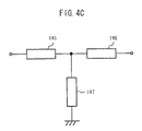
The coupling circuit illustrated in FIG. 4C is an example of a T type coupling circuit. With the T type coupling circuit, the input side and output side are connected by two circuit blocks 145 and 146, and a point between them, and ground, are connected by a circuit block 147. These circuit blocks are realized by a distributed constant element or lumped constant element. The distributed constant element is, for example, a microstrip line, and the lumped constant element is an inductor, a capacitor, or the like. Also the circuit blocks are realized with the individual element or the combination circuit thereof.
The coupling circuit illustrated in FIG. 4D includes a capacitor C1 connected to the signal line connecting the input terminal and output terminal, and two inductors L1 and L2 connected between the signal line and ground.
The coupling circuit illustrated in FIG. 4E illustrates a circuit in which the circuit block 141 includes a plurality of elements. This coupling circuit includes two distributed constant elements 14 b and 14 c, and a capacitor C11, which are connected in series to the signal line, and two inductors L11 and L12 connected between the signal line and ground.
The coupling circuit illustrated in FIG. 4F includes a distributed constant element 14 d connected to the signal line, and two inductors L21 and L22 connected between the signal line and ground.
The coupling circuit illustrated in FIG. 4G illustrates a circuit in which each of the circuit blocks 141 to 143 includes combining an inductor and capacitor connected in parallel. This coupling circuit is a circuit in which a combination of an inductor L31 and capacitor C31 connected in parallel is connected to the signal line, and a combination of an inductor L32 and capacitor C32 connected in parallel, and a combination of an inductor L33 and capacitor C33 connected in parallel, are connected between the signal line and ground.
The coupling circuit illustrated in FIG. 4H is a circuit in which a combination of an inductor L41 and capacitor C41 connected in parallel is connected to the signal line, and two capacitors C42 and C43 are connected between the signal line and ground.
The coupling circuit illustrated in FIG. 4I is a circuit in which a distributed constant element 14 e is connected to the signal line, and a combination of an inductor L51 and capacitor C51 connected in parallel, and a combination of an inductor L52 and capacitor C52 connected in parallel, are connected between the signal line and ground.
The coupling circuit illustrated in FIG. 4J illustrates a circuit including a circuit block 141 in which an inductor and capacitor connected in parallel are combined, and furthermore, a plurality of the combinations are connected. This coupling circuit is a circuit in which a combination of an inductor L60 and capacitor C61 connected in parallel, and a combination of an inductor L61 and capacitor C62 connected in parallel, are connected in series to the signal line, and a combination of an inductor L62 and capacitor C63 connected in parallel, and a combination of an inductor L63 and capacitor C64 connected in parallel, are connected between the signal line and ground.
The coupling circuit illustrated in FIG. 4K is a circuit in which the capacitor C61 and the combination of the inductor L61 and capacitor C62 connected in parallel are connected in series to the signal line, and the combination of the inductor L62 and capacitor C63 connected in parallel, and the combination of the inductor L63 and capacitor C64 connected in parallel, are connected between the signal line and ground.
The coupling circuit illustrated in FIG. 4L is a circuit in which an inductor L71 and a combination of an inductor L72 and capacitor C71 connected in parallel are connected to the signal line, and a combination of an inductor L73 and capacitor C72 connected in parallel, and a combination of an inductor L74 and capacitor C73 connected in parallel, are connected between the signal line and ground.
With a coupling circuit which, being of the π type or T type, includes lumped elements, as illustrated in FIGS. 4E, 4F, and 41 , it is possible to connect a distributed element to one portion.
Also, the π type coupling circuit having two contact points on the signal line connected between the input terminal and output terminal, a lumped constant element or distributed constant element is connected between each contact point and the ground. It is preferable that the elements connected between the contact points and ground have a symmetry. For example, it is preferable that the same element is installed in an a1 section and a2 section in FIG. 4D . In the event of a configuration wherein the same element is installed in the a1 section and a2 section, it is acceptable to install inductors, as illustrated in FIG. 4D or the like, it is acceptable to install capacitors, as illustrated in FIG. 4H , and it is acceptable to install a plurality of lumped constant elements, as illustrated in FIG. 4G or the like.
As illustrated in FIG. 3 , by connecting the resonant lines in parallel to the signal line, and connecting the plurality of resonant lines in the same position in the signal line, it is possible to shorten a line length between the input line 12 a and output line 12 d, in comparison with a filter in which a plurality of resonators having a line length of λ/2 are connected in series, as in a heretofore known technology, so it is possible to reduce the size of the filter in the signal line direction.
Also, with the filter illustrated in FIG. 3 , the paired resonant lines 12 b and 12 c, and the paired resonant lines 12 e and 12 f, are each disposed in positions facing each other across the signal line connecting the input terminal 1 and output terminal 4. By means of this kind of configuration, it is possible to dispose the lines in high density, so it is possible to further reduce the size of the filter in the signal line direction.
With the filter illustrated in FIG. 3 , the electrical length of the resonant lines 12 b, 12 c, 12 e, and 12 f is λ/4, but it is possible to make it (λ/8)×n (λ is a resonant wavelength in the resonator, and n is a positive integer). Even in the event of using resonant lines whose electrical length is, for example, λ/8 (that is, n=1), it is possible to obtain the same advantages. In the event of connecting the resonant lines whose line length is λ/8, one end of each resonant line 12 b, 12 c, 12 e, and 12 f is connected to ground, as illustrated in FIG. 3 . By connecting the resonant lines 12 b, 12 c, 12 e, and 12 f whose line length is λ/8 in this way, signals input from the input terminal 1 are input into the resonant line 12 b via the contact point 13 a, and only a signal which meets the resonant condition of the resonant line 12 b is totally reflected from the ground end, while a signal which does not meet the resonant condition, by being grounded, or reflected to the input side, is attenuated. The signal totally reflected from the ground end of the resonant line 12 b has a phase difference of λ/2 from the signals input into the contact point 13 a from the input terminal 1, and interferes therewith. Because of this, the resonant lines 12 b and 12 c function in combination as one resonator. The resonated signal, after being resonated again in the same way as heretofore described in the resonant lines 12 e and 12 f, via the coupling circuit 14, is output from the output terminal 4 via the output line 12 g. By this means, it is possible to output a desired frequency band signal from the output terminal 4.
A signal, among the signals input into the input terminal 1, which has a wavelength which does not meet the resonant condition of a resonant line, is attenuated by being grounded, or reflected to the input end side, and is prevented from being output from the output terminal 4. By so doing, the filter performs its function.
With the filter illustrated in FIG. 3 , the pair of resonant lines on the input side and the pair of resonant lines on the output side are connected by the one coupling circuit 14. The number of pairs of resonant lines included in the filter not being limited to two, it is possible to connect three or a larger number. A connecting of a much larger number of paired resonant lines may be realized by connecting them by means of a coupling circuit which couples a signal between one pair of resonant lines and another pair of resonant lines, and repeating this kind of connection structure. By this means, the number of resonators included in the whole of the filter increasing, it is possible to realize a filter with a good steepness.
As the first coupling circuit 24 and second coupling circuit 25, it is possible to use the π type coupling circuit or T type coupling circuit. Also, as the π type coupling circuit or T type coupling circuit, it is possible to employ one of the coupling circuits illustrated in FIGS. 4A to 4N . Also, with a coupling circuit which is connected in the π type or T type, includes a lumped constant element, as illustrated in FIGS. 4E, 4F, and 41 , it is possible to connect a distributed constant element to one portion.
In this way, by connecting the resonant lines 22 c and 22 d in parallel in the same portion in the signal line, it being possible to shorten the line length of the signal line connecting the input terminal 1 and output terminal 4, it is possible to reduce the size of the filter in the signal line direction.
Also, with the filter illustrated in FIG. 5 , a description has been given of an example in which the resonant lines 22 c and 22 e are connected to ground, but it is possible to make the terminals thereof connected to ground an open end. In this case, as it is possible to attenuate a filter passband low frequency side signal level in the resonant line 22 b, and attenuate a filter passband high frequency side signal level in the resonant line 22 e, it is possible to improve the steepness of the passband characteristics of the filter.
With the filter illustrated in FIG. 5 , the input side line and output side line are connected by the first coupling circuit 24 and second coupling circuit 25 but, by increasing the number of coupling circuits, it is possible to connect still more paired resonant lines connected between the signal line and ground.
1-3. Ground Sharing of Resonant Lines
It is acceptable that the ground ends of the resonant lines 12 b, 12 c, 12 e, and 12 f illustrated in FIGS. 3 and 5 are connected one to each independent ground, and it is also acceptable that they are connected to an identical ground.
As illustrated by the broken lines in FIG. 6A , in the event that the resonant lines 12 b′ and 12 e′ are disposed so as to be perpendicular to the signal line of which both ends are connected to input and output terminals, and connected to the mutually independent grounds G1′ and G3′, a disposition space of a dimension W2 (W2=W1) is needed in a direction perpendicular to the signal line. In the same way, in the event that the resonant lines 12 c′ and 12 f′ are disposed so as to be perpendicular to the signal line of which both ends are connected to the input and output terminals, and connected to the mutually independent grounds G2′ and G4′, a disposition space of a dimension the same as the dimension W2 is needed in the direction perpendicular to the signal line. Consequently, the size of the filter in the vertical direction (the direction perpendicular to the signal line) is W4 which is approximately twice W2.
As opposed to this, as illustrated by the solid lines in FIG. 6A , by connecting the resonant line 12 b and resonant line 12 e to the ground G1, and disposing them at an angle with respect to the signal line, it is sufficient that a space for disposing the resonant lines 12 b and 12 e is of a dimension W3 (W3<W2) in the direction perpendicular to the signal line. In the same way, by connecting the resonant line 12 c and 12 f to the ground G2, and disposing them at an angle with respect to the signal line, it is sufficient that a space for disposing the resonant lines 12 c and 12 f is of a dimension the same as the dimension W3 in the direction perpendicular to the signal line. Consequently, it is possible to make a dimension W5 (W5=W3×2) of the filter in the vertical direction smaller than a dimension W4. In this way, by connecting a plurality of resonant lines to ground at the same contact point, it is possible to reduce a space in which the resonant lines are disposed.
In this way, by forming the resonant lines 12 b, 12 c, 12 e, and 12 f into the arc shape, it is possible to make a dimension W12 of a resonant line disposition space in the direction perpendicular to the signal line smaller than the dimension W2 illustrated in FIG. 6A . Consequently, it is possible to make a dimension W13 of the filter in the vertical direction (the direction perpendicular to the signal line) smaller than the dimension W4 illustrated in FIG. 6A .
Also, it is possible to make the dimension W12 of the resonant line disposition space in the direction perpendicular to the signal line much smaller than the dimension W3 illustrated in FIG. 6A . Consequently, it is possible to make the dimension W13 of the filter in the vertical direction (the direction perpendicular to the signal line) much smaller than the dimension W5 illustrated in FIG. 6A .
The heretofore described filter configuration which enables miniaturization is also advantageous for a loss reduction. A loss of the filter basically depends on a line conductor loss. By miniaturizing the filter, it being possible to shorten the line length of the filter, it is possible to reduce a signal passing loss.
Also, by miniaturizing the filter, it being possible to increase the number (an available number) of filters which may be fabricated from one wafer at a time of filter manufacture, it is possible to reduce a cost per element.
The filter according to the embodiment may be used as, for example, a small GHz band frequency variable filter using an MEMS variable capacitor.
2. Configuration of Variable Filter
With the capacitance of the resonant lines 12 b, 12 c, 12 e, and 12 f illustrated in FIG. 3 , as a capacitance between them and grounds (to be described hereafter) disposed in a substrate is of a fixed value, the passband of the filter illustrated in FIG. 3 is fixed. As opposed to this, by mounting a movable capacitor electrode (to be described hereafter) on the resonant lines 12 b, 12 c, 12 e, and 12 f, and coupling circuit 14, illustrated in FIG. 3 , it is possible to realize a variable filter which may vary the passband. Also, by mounting a movable capacitor electrode on the resonant lines 22 b, 22 c, 22 d, and 22 e, and coupling circuits 24 and 25 in FIG. 5 , it is possible to realize a variable filter which may vary the passband. By mounting the movable capacitor electrode on the resonant lines, it is possible to shorten the line length and, as well as it being possible to further miniaturize the filter, it is possible to vary the passband. Also, by mounting the movable capacitor electrode on the coupling circuit, it is possible to equivalently change the electrical length of the resonator in such a way as to provide a coupling circuit in accordance with the passband varied in the resonant lines. A description has been given of an example in which these variable filters have the variable capacitors, but it is also acceptable to realize them with variable inductors. Furthermore, it is acceptable to realize the variable filters by appropriately combining the variable capacitors and variable inductors.
In the event that a coupling circuit including only lumped constant elements is installed in the variable filter, as illustrated in FIGS. 4D, 4G, 4H, 4J, 4K, 4L, and 4M , it is sufficient to change at least one lumped constant element, among the lumped constant elements included in the coupling circuit, to a variable element. For example, in the event that the coupling circuit illustrated in FIG. 4D is installed, by changing the capacitor C1 to a variable capacitor, it is possible to realize the coupling circuit in accordance with the passband.
Also, in the event that a coupling circuit including a lumped constant element and distributed constant element is installed in the variable filter, as illustrated in FIGS. 4E, 4F, and 41 , by installing a movable capacitor electrode as the lumped constant element included in the coupling circuit, it is possible to realize the coupling circuit in accordance with the passband.
Also, in the event that a coupling circuit including a plurality of distributed constant elements is installed in the filter, as illustrated in FIG. 4N , by installing a movable capacitor electrode as at least one distributed constant element, among the distributed constant elements 14 f, 14 g, and 14 h included in the coupling circuit, it is possible to realize the variable filter.
By installing the variable capacitor electrode in the resonant lines, as in the embodiment, it being possible to change the capacitance in the resonant lines, it is possible to change a signal passband in the resonant lines. By installing the resonant lines, in which the passband is variable, in the filter in this way, it is possible to realize the variable filter.
Hereafter, a description will be given of a specific configuration of the resonant lines including the movable capacitor electrode (hereafter referred to as the variable capacitor element).
2-1. Configuration of Variable Capacitor Element
The variable capacitor element illustrated in FIGS. 7A and 7B , including a substrate 31, a signal line 32, movable capacitor electrodes 33, drive electrodes 35 a and 35 b, a dielectric dot 36, anchor sections 37 a and 37 b, electrode pads 38, and a packaging member 39, is configured as one portion of a filter which allows a passage of an electromagnetic wave or electrical signal in a specified high frequency band. The packaging member 39 seals not only a variable capacitor element section, but the whole of the filter.
The substrate 31 is an LTCC wafer (LTCC: Low Temperature Co-fired Ceramics) including multilayer internal wirings (wiring patterns 31 c). The substrate 31 is formed by mutually bonding a plurality (five in the substrate illustrated in FIG. 7B ) of insulating layers 31 a. A via 31 b which includes a conductive portion in a through hole formed from one principal surface to the other principal surface is formed in each insulating layer 31 a. Also, each wiring pattern 31 c is sandwiched between at least one pair of adjacent insulating layers 31 a. Also, one portion of the wiring pattern 31 c positioned on a side of the substrate 31 closest to a first surface 31 e is a ground line 31 d connected to ground. The ground line 31 d faces the signal line 32 across the insulating layer 31 a, and the ground line 31 d and signal line 32 have a gap CG2 between them. Regarding the ground line 31 d illustrated in FIG. 7B , an example has been described in which it is disposed in a position close to the first surface but, it not being limited to this, it is also acceptable to dispose it on another layer. In this case, the ground line 31 d faces the signal line 32 across a plurality of the insulating layers 31 a. For this reason, the gap CG2 between the ground line 31 d and signal line 32 is equivalent to a thickness to which the plurality of insulating layers 31 a are stacked. Also, the wiring patterns 31 c are connected, and the wiring patterns 31 c and electrode pads 38 are connected, by the vias 31 b. In some cases, it is acceptable that the wiring patterns 31 c and signal line 32 are connected by the vias 31 b. Also, the insulating layers 31 a are realized by an LTCC. However, their not being limited to the LTCC, it is acceptable to form them from another dielectric body.
The signal line 32, as illustrated in FIG. 7A , including a terminal 32 a and terminal 32 b at both ends in its longitudinal direction, is a conductor pattern in which an electrical signal passes between the terminals 32 a and 32 b. The terminals 32 a and 32 b, by being connected to other elements on the wiring substrate, or made an open end, are electrically connected to predetermined electrode pads 38 via predetermined vias 31 b and wiring patterns 31 c in the wiring substrate 31 (not illustrated). Also, the signal line 32, being a distributed constant transmission line of which the impedance is, for example, 20Ω, is formed from a low resistance metal material such as, for example, Cu, Ag, Au, Al, W, or Mo. Also, the thickness of the signal line 32 is, for example, 0.5 to 20 μm.
Both ends of each movable capacitor electrode 33 are fixed to the anchor sections 37 a and 37 b formed on the first surface 31 e of the substrate 31, and a main portion thereof excluding both ends faces the signal line 32 and drive electrodes 35 a and 35 b across an air gap. A thick section 33 a is formed in a portion of each movable capacitor electrode 33 facing the signal line 32. The thick sections 33 a and signal line 32 face each other across a gap CG1. The movable capacitor electrodes 33 are connected to ground via the anchor sections 37 a and 37 b, vias 31 b, and wiring patterns 31 c. The movable capacitor electrodes 33, being formed from an elastically deformable material, may be formed from, for example, a low resistance metal such as, for example, Au, Cu, or Al. The variable capacitor element whose capacitance changes is realized by the movable capacitor electrodes 33 being moved to change a distance between the movable capacitor electrodes 33 and signal line 32. Also, the gap CG1 between the movable capacitor electrodes 33 and signal line 32 may be made, for example, 0.1 to 10 μm. Also, the movable capacitor electrodes 33 and ground line 31 d are one example of a ground wiring section in the embodiment.
The drive electrodes 35 a and 35 b, being disposed adjacent to the signal line 32, face one portion of each movable capacitor electrode 33. The drive electrodes 35 a and 35 b generate an electrostatic attractive force between themselves and the movable capacitor electrodes 33, enabling the movable capacitor electrodes 33 to be displaced in a direction indicated by an arrow A. By the movable capacitor electrodes 33 being displaced by the action of the drive electrodes 35 a and 35 b, a capacitance between the signal line 32 and movable capacitor electrodes 33 changes. The drive electrodes 35 a and 35 b are formed from a high resistance metal thin film such as, for example, a SiCr thin film. Also, in order to suppress an occurrence of a pull-in phenomenon, it is preferable that a gap between the drive electrodes 35 a and 35 b and movable capacitor electrodes 33 is made equal to or more than three times the gap CG1 between the movable capacitor electrodes 33 and signal line 32.
The dielectric dot 36, being provided on the signal line 32, is formed from a dielectric material such as, for example, Al2O3, SiO2, SixNy, or SiOC. The dielectric dot 36, as well as being able to prevent the signal line 32 and movable capacitor electrodes 33 from short circuiting, may increase a capacitance occurring in the gap CG1 between the signal line 32 and movable capacitor electrodes 33. It is preferable to increase the capacitance because it is thereby possible to ensure a wide filter frequency variable range.
The packaging member 39 seals structures of the filter which, being bonded to the first surface 31 e of the substrate 31, are formed on the first surface 31 e of the substrate 31.
In the variable capacitor element illustrated in FIGS. 7A and 7B , a first capacitor is formed by the gap CG2 being formed between the signal line 32 and the ground line 31 d disposed in the substrate 31. Also, a second capacitor is formed by the gap CG1 being formed between the signal line 32 and movable capacitor electrodes 33. By forming two capacitors in this way, it is possible to increase the capacitance. Consequently, with these capacitors, it is possible to increase the capacitance in comparison with a microstrip line or distributed constant element which includes only the first capacitor, as heretofore known. That is, with these capacitors, it is possible to increase the capacitance in comparison with a microstrip line or distributed constant element which includes no movable capacitor electrode. By increasing the capacitance, it is possible to shorten the physical signal line length of a resonant line including a variable distributed constant element. Therefore, by installing this kind of variable capacitor element in the filter, it being possible to shorten the line length of the resonant line, it is possible to miniaturize the filter.
Also, by applying a voltage to the drive electrodes 35 a and 35 b via the electrode pads 38, vias 31 b and wiring patterns 31 c, it is possible to generate an electrostatic attractive force between the drive electrodes 35 a and 35 b and movable capacitor electrodes 33, and elastically displace the movable capacitor electrodes 33 in the direction indicated by the arrow A. By displacing the movable capacitor electrodes 33, it is possible to reduce the gap CG1 between the signal line 32 and movable capacitor electrodes 33. By reducing the gap CG1, it is possible to increase the capacitance in the second capacitor. By increasing the capacitance, the line length of the distributed constant element increases equivalently or essentially, and a resonated frequency band is shifted to a low frequency side.
Also, the drive electrodes 35 a and 35 b, as well as being divided for each movable capacitor electrode 33, are configured so that a voltage may be applied to each individual one. Then, by selectively applying a voltage to the divided drive electrodes 35 a and 35 b, the plurality of movable capacitor electrodes 33 are selectively displaced. The movable capacitor electrodes 33 are selectively displaced, thereby enabling changes in capacitance to differ in magnitude.
Also, as the electrostatic attractive force occurring between the drive electrodes 35 a and 35 b and movable capacitor electrodes 33 is diminished by decreasing the voltage applied to the drive electrodes 35 a and 35 b, a displacement amount of the movable capacitor electrodes 33 decreases, enabling the movable capacitor electrodes 33 to return in a direction indicated by an arrow B. By returning the movable capacitor electrodes 33 in the direction indicated by the arrow B, the gap CG1 between the signal line 32 and movable capacitor electrodes 33 increases, and the capacitance in the second capacitor decreases. By the capacitance decreasing, the electrical length of the distributed constant element decreases equivalently or essentially.
In this way, by adjusting the voltage applied to the drive electrodes 35 a and 35 b, and displacing the movable capacitor electrodes 33 in a direction approaching the signal line 32, it is possible to make the second capacitor a variable capacitor, and it is possible to change a signal passing frequency band in the variable filter element. It is possible to realize the variable filter by installing this kind of variable capacitor element in, for example, the resonant lines 12 b, 12 c, 12 e, and 12 f, and coupling circuit 14 illustrated in FIG. 3 , or the resonant lines 22 b, 22 c, 22 d, and 22 e, and coupling circuit 24 illustrated in FIG. 5 .
Also, with a commonly known CPW signal line, a signal line (one being an example) and ground lines (for example, two) being provided on the same surface of a substrate, as a drive electrode for driving a movable capacitor electrode is disposed between the signal line and the ground lines, there is a limitation on a drive electrode disposition space, and there is a limit to increasing the area of the drive electrode. As opposed to this, as the variable filter element using the microstrip line, illustrated in FIGS. 7A and 7B has no ground line provided on a surface of the substrate the same as the surface on which the signal line is formed, it is possible to secure a large area of the drive electrodes 35 a and 35 b on the substrate 31. By securing the large area of the drive electrodes 35 a and 35 b, it being possible to reduce the voltage applied to the drive electrodes 35 a and 35 b when displacing the movable capacitor electrode 33, it is possible to secure a wide movable range of the movable capacitor electrodes 33. Also, by reducing the drive voltage, it is possible to reduce a power consumption.
Also, it is conceivable that, by increasing the area of the drive electrodes 35 a and 35 b, it is possible to suppress a self-actuation phenomenon due to a high frequency signal. That is, as it is possible, by increasing the area of the drive electrodes 35 a and 35 b, to increase the electrostatic attractive force occurring between the drive electrodes 35 a and 35 b and movable capacitor electrodes 33, it is possible to form the movable capacitor electrodes 33 from an elastic body with a high rigidity. Furthermore, the higher the area ratio of the drive electrodes 35 a and 35 b and a capacitor section CAP, a coulomb force occurring between the signal line 32 and movable capacitor electrodes 33 due to a high frequency signal passing through the capacitor section CAP becomes negligible compared with a coulomb force occurring between the drive electrodes 35 a and 35 b and movable capacitor electrodes 33 due to the drive voltage. Consequently, in the embodiment, it is conceivable that the increase in the area of the drive electrodes 35 a and 35 b is advantageous for a suppression of the self-actuation phenomenon of a parallel plate type variable capacitor.
2-2. Method of Manufacturing Variable Filter Element
Firstly, as illustrated in FIG. 8A , the electrode pads 38 are formed on a second surface 31 f of the substrate 31 including the multilayer internal wirings. The electrode pads 38 may be formed by, for example, after forming a predetermined metal material as a film on the second surface 31 f of the substrate 31 by means of a sputtering method, patterning the metal film by means of a predetermined wet etching or dry etching. Alternatively, in the formation of the electrode pads 38, it is possible to employ a nonelectrolytic plating method or electroplating method. Next, the drive electrodes 35 a and 35 b are formed on the first surface 31 e of the substrate 31. The drive electrodes 35 a and 35 b may be formed by, for example, after forming a predetermined metal material as a film on the substrate 31 by means of a sputtering method, patterning the metal film by means of a predetermined wet etching or dry etching. It is also acceptable that, after the process of forming the drive electrodes 35 a and 35 b, a process of forming an insulating film is implemented in such a way as to cover the drive electrodes 35 a and 35 b. Next, the signal line 32 and anchor sections 37 a and 37 b are formed on the first surface 31 e of the substrate 31. The signal line 32 may be formed by, for example, after forming a resist pattern, which has openings corresponding to the signal line 32 and anchor sections 37 a and 37 b, on the substrate 31 by means of a patterning, depositing a predetermined metal material (for example, Au), and causing it to grow, in the openings by means of a plating method (a nonelectrolytic plating or electroplating).
Next, as illustrated in FIG. 8B , the dielectric dot 36 is formed on the signal line 32. The dielectric dot 36 may be formed by, for example, after forming a predetermined dielectric film on the first surface 31 e side of the substrate 31, patterning the dielectric film.
Next, as illustrated in FIG. 8C , a sacrifice layer 40 is formed. The sacrifice layer 40 is formed from a material which, being easy to remove, may be selectively etched.
Next, as illustrated in FIG. 8D , the movable capacitor electrode 33 is formed on the sacrifice layer 40. The movable capacitor electrode 33 may be formed by, for example, after forming a predetermined metal material as a film on the sacrifice layer 40 by means of a sputtering method, patterning the metal film by means of a predetermined wet etching or dry etching. Alternatively, the movable capacitor electrode 33 may be formed by employing a nonelectrolytic plating method or electroplating method
Next, as illustrated in FIG. 8E , the thick section 33 a forming one portion of the movable capacitor electrode 33 is formed. The thick section 33 a may be formed by, for example, after forming a resist pattern, which has an opening corresponding to the thick section 33 a, over the movable capacitor electrode 33 and sacrifice layer 40 by means of a patterning, depositing a predetermined metal material (for example, Au), and causing it to grow, in the opening by means of a plating method (a nonelectrolytic plating or electroplating).
Next, as illustrated in FIG. 8F , the sacrifice layer 40 is removed. By this means, it is possible to form an air gap between the movable capacitor electrode 33 and the signal line 32, drive electrodes 35 a and 35 b, and dielectric dot 36.
Next, as illustrated in FIG. 8G , the packaging member 39 is bonded to the first surface 31 e side of the substrate 31. As a method of bonding the packing member 39 to the substrate 31, it is possible to propose, for example, an anodic bonding method, a direct bonding method, a room temperature bonding method, and a eutectic bonding method. The packaging member 39 being one fabricated by processing an LTCC, a concavity 39 a is provided in advance in a portion corresponding to each variable filter formation section of the substrate 31.
Next, the substrate 31 and packaging member 39 are cut into individual variable filters.
By the above means, the variable filter is completed.
The LTCC has been used for the packaging member, but it is also possible to use a dielectric body, such as a resin or ceramic, or a high resistance silicon.
3. Configuration of Communication Module
When carrying out a receiving operation, the reception filter 62 a allows only a predetermined frequency band signal, among received signals input via an antenna terminal 61, to pass through, and outputs it from the receiving terminals 63 a and 63 b to the exterior. Also, when carrying out a transmitting operation, the transmission filter 62 b allows only a predetermined frequency band signal, among transmission signals input from the transmitting terminal 65 and amplified by the power amplifier 64, to pass through, and outputs it from the antenna terminal 61 to the exterior.
Also, FIG. 10 illustrates a communication module which includes a variable reception filter 66 a in place of the reception filter 62 a in the communication module illustrated in FIG. 9 , and a variable transmission filter 66 b in place of the transmission filter 62 b. The variable reception filter 66 a and variable transmission filter 66 b include the variable filter described in the section “2. Configuration of Variable Filter” in the present specification. With a reception filter and transmission filter which cannot vary the passband, in the event of attempting to realize a multiband compatible communication module which may transmit and receive a plurality of high frequency signals in differing frequency bands, the communication module includes reception filters and transmission filters corresponding to the frequency bands, and a switch circuit which switches between the filters for each of the frequency bands in which to transmit and receive the signals, meaning that the communication module is larger in size. As opposed to this, according to the communication module illustrated in FIG. 10 , by its including one variable reception filter 66 a and one variable transmission filter 66 b, it is possible to reduce the number of filters, and it is possible to downsize the multiband compatible communication module.
By including the passband filter of the embodiment in the reception filter 62 a and transmission filter 62 b of the communication module, as heretofore described, it is possible to downsize the communication module. That is, with a heretofore known filter, as a configuration has been employed wherein a plurality of resonant lines are connected in series, the size in the signal line direction has been increased but, in the embodiment, as a configuration is employed wherein the plurality of resonant lines are connected in parallel in the same position, it is possible to reduce the size of the filter in the signal line direction. Consequently, by mounting the miniaturized filter, it is possible to downsize the communication module. In particular, with a communication module which carries out a high frequency band communication, the number of filters becomes larger, by mounting a filter of which the size in the signal line direction is small, as in the embodiment, it is possible to downsize the communication module. In particular, as the number of filters becomes larger with the communication module which carries out the high frequency band communication, by mounting a filter of which the size in the signal line direction is small, as in the embodiment, it is possible to downsize a communication module compatible with the high frequency band communication.
Also, as it is possible to reduce the passing loss by miniaturizing the filter, it is possible to realize a communication module with superior communication characteristics.
The configurations of the communication modules illustrated in FIGS. 9 and 10 being one example, it is also possible to obtain the same advantages when mounting the passband filter of the embodiment in a communication module of another form.
4. Configuration of Communication Apparatus
Firstly, an LSI to be operated is selected by an antenna switch circuit 72 depending on whether a communication system compatible with a received signal input via an antenna 71 is of the W-CDMA or GSM. In the event that the received signal input is compatible with the W-CDMA communication system, the received signal is switched in such a way as to be output to a duplexer 73. The received signal input into the duplexer 73 is limited to a predetermined frequency band by the reception filter 73 a, and a balanced type received signal is output to an LNA 74. The LNA 74 amplifies the input received signal, and outputs it to an LSI 76. The LSI 76, based on the input received signal, carries out a process of demodulation into a sound signal, and controls the drive of each section in the portable telephone terminal.
Meanwhile, when transmitting signals, the LSI 76 generates transmission signals. The generated transmission signals are amplified by a power amplifier 75, and input into the transmission filter 73 b. The transmission filter 73 b causes only a predetermined frequency band signal, among the input transmission signals, to pass through. The transmission signal output from the transmission filter 73 b is output from the antenna 71 to the exterior, via the antenna switch circuit 72.
Also, in the event that the input received signal is a signal compatible with the GSM communication system, the antenna switch circuit 72 selects one of the reception filters 77 to 80 in accordance with the frequency band, and outputs the received signal. The received signal subjected to a band limitation by the selected one of the reception filters 77 to 80 is input into an LSI 83. The LSI 83, based on the input received signal, carries out a process of demodulation into a sound signal, and controls the drive of each section in the portable telephone terminal. Meanwhile, when transmitting signals, the LSI 83 generates transmission signals. The generated transmission signals are amplified by a power amplifier 81 or 82, and output from the antenna 71 to the exterior, via the antenna switch circuit 72.
Also, FIG. 12 illustrates a communication apparatus which includes a variable reception filter 84 in place of the reception filter 73 a in the communication apparatus illustrated in FIG. 11 , and includes a variable transmission filter 85 in place of the transmission filter 73 b. Also, the communication apparatus includes a variable reception filter 86 in place of the reception filters 77, 78, 79, and 80. The variable reception filters 84 and 86, and variable transmission filter 85, include the variable filter described in the section “2. Configuration of Variable Filter” in the embodiment. Although not illustrated, the passbands in the variable reception filters 84 and 86, and variable transmission filter 85, are adjusted by a separately provided control circuit.
As heretofore described, by installing in the communication apparatus the filter of which the size in the signal line direction is reduced, it is possible to downsize the communication apparatus. That is, with the heretofore known filter, as a configuration has been employed wherein the plurality of resonant lines are connected in series, the size in the signal line direction has been increased but, in the embodiment, as a configuration is employed wherein the plurality of resonant lines are connected in parallel in the same position, it is possible to reduce the size of the filter in the signal line direction. Consequently, by mounting the miniaturized filter, it is possible to downsize the communication apparatus. In particular, as the number of filters becomes larger with the communication module which carries out a high frequency band communication, by mounting the filter of which the size in the signal line direction is small, as in the embodiment, it is possible to downsize the communication apparatus compatible with the high frequency band communication.
Also, by installing the variable filter, it is possible to selectively transmit and receive a plurality of frequency band signals using one filter, meaning that, it being possible to reduce the number of filters, it is possible to downsize the communication apparatus. Also, as it is possible to reduce the passing loss by miniaturizing the filter, it is possible to realize the communication apparatus with superior communication characteristics.
The communication apparatus of the embodiment is useful for a mobile communication apparatus of which the usable frequency band is approximately 800 MHz to 6 GHz, in particular, a mobile communication apparatus which carries out communication using a frequency band of 2 GHz or higher.
5. Advantages of Embodiment, and Other
According to the embodiment, by connecting a resonant line functioning as a resonator between a signal line and ground, and connecting a plurality of the resonant lines in the same position in the signal line, it is possible to shorten the line length in the signal line direction in comparison with a configuration wherein a plurality of resonant lines are connected in series in the signal line direction, as in the heretofore known technology, so it is possible to reduce the size of the filter in the signal line direction.
Also, by connecting one end of each of the resonant lines to ground, it is possible to shorten the line length of the resonant lines. In the event that the resonant lines are connected in series to the signal line, as in the heretofore known technology, the line length of the resonant lines has been λ/2 but, by connecting the resonant lines in parallel to the signal line, and connecting one end of each of the resonant lines to ground, as in the embodiment, it is possible to totally reflect a signal which meets the resonant condition, so it is possible to make the length of the resonant lines λ/8×n (n is a positive integer).
Also, by adopting a configuration wherein the resonant lines are connected in parallel to the signal line, it is possible to mount them in high density on the substrate, so it is possible to miniaturize the filter.
Also, by adopting a configuration wherein a plurality of the resonant lines are connected to a common ground, it is possible to dispose the resonant lines at an angle with respect to the signal line, so it is possible to reduce the size of the filter in the vertical direction (the direction perpendicular to the signal line).
Also, as well as connecting a plurality of the resonant lines to a common ground, by forming the resonant lines, of each of which one end is connected to the signal line, and the other end is connected to the ground, into an approximate arc shape, it is possible to reduce the size of the filter in the vertical direction (the direction perpendicular to the signal line).
Also, by suspending the capacitor electrodes on the resonant lines, it is possible to increase the capacitance in the resonant lines, meaning that, it being possible to shorten the physical line length of the resonant lines, it is possible to reduce the size of the filter in the vertical direction (the direction perpendicular to the signal line).
Also, by suspending the variable capacitor electrodes on the resonant lines, and changing the capacitance in the resonant lines by displacing the variable capacitor electrodes, it is possible to equivalently change the electrical length, so it is possible to realize the variable filter. By employing the variable filter as the reception filter and the transmission filter in the communication module and communication apparatus, there is no need to install the transmission filter and reception filter for each passband in the multiband compatible communication module and communication apparatus, so it is possible to downsize the communication module and communication apparatus.
Also, by miniaturizing the filter, it being possible to increase the number of filter modules which may be obtained from one wafer at the time of filter manufacture, it is possible to reduce a manufacturing cost.
All examples and conditional language recited herein are intended for pedagogical purposes to aid the reader in understanding the principles of the invention and the concepts contributed by the inventor to furthering the art, and are to be construed as being without limitation to such specifically recited examples and conditions, nor does the organization of such examples in the specification relate to a showing of the superiority and inferiority of the invention. Although the embodiments of the present inventions have been described in detail, it should be understood that the various changes, substitutions, and alterations could be made hereto without departing from the spirit and scope of the invention.
Claims (5)
1. A filter comprising:
a substrate;
a signal line formed on the substrate and including an input terminal and an output terminal at either end of the signal line;
a first pair of resonant lines connected between the signal line and a ground portion, wherein one ends of the first pair of resonant lines are connected to the signal line at a first point;
a second pair of resonant lines connected between the signal line and the ground portion, wherein one ends of the second pair of resonant lines are connected to the signal line at a second point; and
a coupling section provided between the first pair of resonant lines and the second pair of resonant lines,
wherein each of the first pair of resonant lines and each of the second pair of resonant lines are provided obliquely with respect to the signal line, the other end of one of the first pair of resonant lines and the other end of one of the second pair of resonant lines are connected to the ground portion at a third point, and the other end of the other of the first pair of resonant lines and the other end of the other of the second pair of resonant lines are connected to the ground portion at a fourth point,
wherein the coupling section includes a distributed constant element connected to the signal line and two inductors connected between the signal line and the ground portion,
wherein one end of the distributed constant element is connected to the input terminal via the signal line, and the other end of the distributed constant element is connected to the output terminal via the signal line.
2. The filter according to claim 1 , wherein the first point is positioned at a side of the input terminal and the second point is positioned at a side of the output terminal.
3. The filter according to claim 1 , wherein one end of one of the two inductors is connected to the signal line at the first point, the other end of the one of the two inductors is connected to the ground portion at the third point, one end of the other of the two inductors is connected to the signal line at the second point, and the other end of the other of the two inductors is connected to the ground portion at the fourth point.
4. The filter according to claim 1 , wherein the first pair of resonant lines and the second pair of resonant lines are formed into an arc shape.
5. The filter according to claim 1 , wherein the substrate is a ceramic substrate including a plurality of laminated internal wirings.
Priority Applications (1)
| Application Number | Priority Date | Filing Date | Title |
|---|---|---|---|
| US15/150,882 US9876479B2 (en) | 2008-12-25 | 2016-05-10 | Filter |
Applications Claiming Priority (5)
| Application Number | Priority Date | Filing Date | Title |
|---|---|---|---|
| JP2008329360A JP5294013B2 (en) | 2008-12-25 | 2008-12-25 | Filter, communication module, and communication device |
| JP2008-329360 | 2008-12-25 | ||
| US12/632,098 US20100164652A1 (en) | 2008-12-25 | 2009-12-07 | Filter, communication module, and communication apparatus |
| US14/102,974 US20140097915A1 (en) | 2008-12-25 | 2013-12-11 | Filter, communication module, and communication apparatus |
| US15/150,882 US9876479B2 (en) | 2008-12-25 | 2016-05-10 | Filter |
Related Parent Applications (1)
| Application Number | Title | Priority Date | Filing Date |
|---|---|---|---|
| US14/102,974 Division US20140097915A1 (en) | 2008-12-25 | 2013-12-11 | Filter, communication module, and communication apparatus |
Publications (2)
| Publication Number | Publication Date |
|---|---|
| US20160254796A1 US20160254796A1 (en) | 2016-09-01 |
| US9876479B2 true US9876479B2 (en) | 2018-01-23 |
Family
ID=41694468
Family Applications (3)
| Application Number | Title | Priority Date | Filing Date |
|---|---|---|---|
| US12/632,098 Abandoned US20100164652A1 (en) | 2008-12-25 | 2009-12-07 | Filter, communication module, and communication apparatus |
| US14/102,974 Abandoned US20140097915A1 (en) | 2008-12-25 | 2013-12-11 | Filter, communication module, and communication apparatus |
| US15/150,882 Active 2029-12-15 US9876479B2 (en) | 2008-12-25 | 2016-05-10 | Filter |
Family Applications Before (2)
| Application Number | Title | Priority Date | Filing Date |
|---|---|---|---|
| US12/632,098 Abandoned US20100164652A1 (en) | 2008-12-25 | 2009-12-07 | Filter, communication module, and communication apparatus |
| US14/102,974 Abandoned US20140097915A1 (en) | 2008-12-25 | 2013-12-11 | Filter, communication module, and communication apparatus |
Country Status (5)
| Country | Link |
|---|---|
| US (3) | US20100164652A1 (en) |
| EP (1) | EP2202840B1 (en) |
| JP (1) | JP5294013B2 (en) |
| KR (1) | KR101097701B1 (en) |
| CN (1) | CN101764593B (en) |
Cited By (1)
| Publication number | Priority date | Publication date | Assignee | Title |
|---|---|---|---|---|
| US11431069B2 (en) | 2019-02-28 | 2022-08-30 | KYOCERA AVX Components Corporation | High frequency, surface mountable microstrip band pass filter |
Families Citing this family (1)
| Publication number | Priority date | Publication date | Assignee | Title |
|---|---|---|---|---|
| CN103532511B (en) * | 2013-10-08 | 2016-11-16 | 桂林市思奇通信设备有限公司 | A kind of combiner with splitter functionality |
Citations (24)
| Publication number | Priority date | Publication date | Assignee | Title |
|---|---|---|---|---|
| US2964718A (en) | 1955-03-21 | 1960-12-13 | Cutler Hammer Inc | Microwave circuits |
| JPS6230402A (en) | 1985-08-01 | 1987-02-09 | Murata Mfg Co Ltd | Band elimination filter |
| JPH0537244A (en) | 1991-07-31 | 1993-02-12 | Sanyo Electric Co Ltd | Mixer circuit |
| JPH05175701A (en) | 1991-12-25 | 1993-07-13 | Matsushita Electric Ind Co Ltd | Band pass filter |
| US5334961A (en) | 1991-08-12 | 1994-08-02 | Matsushita Electric Industrial Co., Ltd. | Strip-line type bandpass filter |
| US5808527A (en) | 1996-12-21 | 1998-09-15 | Hughes Electronics Corporation | Tunable microwave network using microelectromechanical switches |
| JPH10335903A (en) | 1997-05-28 | 1998-12-18 | Sharp Corp | Voltage-controlled passband variable filter, voltage-controlled resonance frequency variable resonator, and high-frequency circuit module using them |
| US5923232A (en) | 1997-07-11 | 1999-07-13 | Honeywell Inc. | Mechanism for elimination of corona effect in high power RF circuitry at extended altitudes |
| US6054908A (en) | 1997-12-12 | 2000-04-25 | Trw Inc. | Variable bandwidth filter |
| JP2001007682A (en) | 1999-06-17 | 2001-01-12 | Hitachi Kokusai Electric Inc | Tuning frequency variable filter |
| WO2003017417A1 (en) | 2001-08-20 | 2003-02-27 | Xytrans, Inc. | Millimeter wave filter for surface mount applications |
| JP2003309401A (en) | 2002-04-17 | 2003-10-31 | Mitsubishi Electric Corp | Filter circuit and frequency multiplier circuit using the filter circuit |
| JP2003332805A (en) | 2002-05-10 | 2003-11-21 | Matsushita Electric Ind Co Ltd | High frequency filter and substrate for high frequency module |
| US20050052262A1 (en) * | 2003-09-04 | 2005-03-10 | Tdk Corporation | Multi-layer band-pass filter |
| US20050068126A1 (en) | 2003-09-30 | 2005-03-31 | Akira Muto | Resonator and dielectric filter |
| WO2005088832A1 (en) | 2004-03-16 | 2005-09-22 | Nec Corporation | Filter circuit |
| US20060087388A1 (en) | 2004-10-27 | 2006-04-27 | Ntt Docomo, Inc. | Resonator |
| WO2007029853A1 (en) | 2005-09-05 | 2007-03-15 | Matsushita Electric Works, Ltd. | Bandpass filter and resonator |
| US20070069838A1 (en) * | 2005-09-29 | 2007-03-29 | Hiroyuki Kayano | Filter and radio communication device using the same |
| EP1783854A1 (en) | 2005-11-08 | 2007-05-09 | NTT DoCoMo Inc. | Variable resonator |
| US20070149159A1 (en) | 2005-12-23 | 2007-06-28 | Hiroyuki Kayano | Filter circuit and radio communication system comprising filter |
| EP1986319A2 (en) | 2007-04-27 | 2008-10-29 | Fujitsu Limited | Variable filter element, variable filter module and fabrication method thereof |
| US7889029B2 (en) | 2006-03-24 | 2011-02-15 | National Taiwan University | Active bandpass filter |
| US7944330B2 (en) | 2008-03-06 | 2011-05-17 | Funai Electric Co., Ltd. | Resonant element and high frequency filter, and wireless communication apparatus equipped with the resonant element or the high frequency filter |
Family Cites Families (6)
| Publication number | Priority date | Publication date | Assignee | Title |
|---|---|---|---|---|
| JPS58141005A (en) * | 1982-02-17 | 1983-08-22 | Sony Corp | Band-pass filter for microwave |
| US20030016099A1 (en) * | 2001-07-23 | 2003-01-23 | Manseau David J. | Tunable resonator and method of tuning the same |
| JP2004363961A (en) * | 2003-06-05 | 2004-12-24 | Sony Corp | High-frequency signal filter device and electronic appliance |
| US7372373B2 (en) * | 2004-08-27 | 2008-05-13 | Itron, Inc. | Embedded antenna and filter apparatus and methodology |
| JP4176752B2 (en) * | 2004-09-03 | 2008-11-05 | 太陽誘電株式会社 | filter |
| JP4621155B2 (en) * | 2006-02-28 | 2011-01-26 | 株式会社エヌ・ティ・ティ・ドコモ | Variable filter |
-
2008
- 2008-12-25 JP JP2008329360A patent/JP5294013B2/en not_active Expired - Fee Related
-
2009
- 2009-12-07 US US12/632,098 patent/US20100164652A1/en not_active Abandoned
- 2009-12-10 EP EP09178755.6A patent/EP2202840B1/en not_active Not-in-force
- 2009-12-24 KR KR1020090131034A patent/KR101097701B1/en active IP Right Grant
- 2009-12-25 CN CN2009102655261A patent/CN101764593B/en not_active Expired - Fee Related
-
2013
- 2013-12-11 US US14/102,974 patent/US20140097915A1/en not_active Abandoned
-
2016
- 2016-05-10 US US15/150,882 patent/US9876479B2/en active Active
Patent Citations (28)
| Publication number | Priority date | Publication date | Assignee | Title |
|---|---|---|---|---|
| US2964718A (en) | 1955-03-21 | 1960-12-13 | Cutler Hammer Inc | Microwave circuits |
| JPS6230402A (en) | 1985-08-01 | 1987-02-09 | Murata Mfg Co Ltd | Band elimination filter |
| JPH0537244A (en) | 1991-07-31 | 1993-02-12 | Sanyo Electric Co Ltd | Mixer circuit |
| US5334961A (en) | 1991-08-12 | 1994-08-02 | Matsushita Electric Industrial Co., Ltd. | Strip-line type bandpass filter |
| JPH05175701A (en) | 1991-12-25 | 1993-07-13 | Matsushita Electric Ind Co Ltd | Band pass filter |
| US5808527A (en) | 1996-12-21 | 1998-09-15 | Hughes Electronics Corporation | Tunable microwave network using microelectromechanical switches |
| JPH10335903A (en) | 1997-05-28 | 1998-12-18 | Sharp Corp | Voltage-controlled passband variable filter, voltage-controlled resonance frequency variable resonator, and high-frequency circuit module using them |
| US5923232A (en) | 1997-07-11 | 1999-07-13 | Honeywell Inc. | Mechanism for elimination of corona effect in high power RF circuitry at extended altitudes |
| US6054908A (en) | 1997-12-12 | 2000-04-25 | Trw Inc. | Variable bandwidth filter |
| JP2001007682A (en) | 1999-06-17 | 2001-01-12 | Hitachi Kokusai Electric Inc | Tuning frequency variable filter |
| WO2003017417A1 (en) | 2001-08-20 | 2003-02-27 | Xytrans, Inc. | Millimeter wave filter for surface mount applications |
| JP2005500773A (en) | 2001-08-20 | 2005-01-06 | ザイトランス・インコーポレーテッド | Millimeter wave filter for surface mount applications |
| JP2003309401A (en) | 2002-04-17 | 2003-10-31 | Mitsubishi Electric Corp | Filter circuit and frequency multiplier circuit using the filter circuit |
| JP2003332805A (en) | 2002-05-10 | 2003-11-21 | Matsushita Electric Ind Co Ltd | High frequency filter and substrate for high frequency module |
| US20050052262A1 (en) * | 2003-09-04 | 2005-03-10 | Tdk Corporation | Multi-layer band-pass filter |
| US20050068126A1 (en) | 2003-09-30 | 2005-03-31 | Akira Muto | Resonator and dielectric filter |
| KR20050031929A (en) | 2003-09-30 | 2005-04-06 | 소니 가부시끼 가이샤 | Resonator and dielectric filter |
| WO2005088832A1 (en) | 2004-03-16 | 2005-09-22 | Nec Corporation | Filter circuit |
| US20060087388A1 (en) | 2004-10-27 | 2006-04-27 | Ntt Docomo, Inc. | Resonator |
| JP2006128912A (en) | 2004-10-27 | 2006-05-18 | Ntt Docomo Inc | Resonator and variable resonator |
| WO2007029853A1 (en) | 2005-09-05 | 2007-03-15 | Matsushita Electric Works, Ltd. | Bandpass filter and resonator |
| US20070069838A1 (en) * | 2005-09-29 | 2007-03-29 | Hiroyuki Kayano | Filter and radio communication device using the same |
| EP1783854A1 (en) | 2005-11-08 | 2007-05-09 | NTT DoCoMo Inc. | Variable resonator |
| US20070149159A1 (en) | 2005-12-23 | 2007-06-28 | Hiroyuki Kayano | Filter circuit and radio communication system comprising filter |
| JP2007174438A (en) | 2005-12-23 | 2007-07-05 | Toshiba Corp | Filter circuit and radio communication system with filter |
| US7889029B2 (en) | 2006-03-24 | 2011-02-15 | National Taiwan University | Active bandpass filter |
| EP1986319A2 (en) | 2007-04-27 | 2008-10-29 | Fujitsu Limited | Variable filter element, variable filter module and fabrication method thereof |
| US7944330B2 (en) | 2008-03-06 | 2011-05-17 | Funai Electric Co., Ltd. | Resonant element and high frequency filter, and wireless communication apparatus equipped with the resonant element or the high frequency filter |
Non-Patent Citations (8)
| Title |
|---|
| European Office Action dated Jan. 18, 2011, issued in corresponding European Patent Application No. 09178755.6. (1 page). |
| European Search Report dated Mar. 5, 2010, issued in corresponding European Patent Application No. 09178755.6. (6 pages). |
| Fourn, E et al, "MEMS Switchable Interdigital Coplanar Filter," IEEE Transactions on Microwave Theory and Techniques, vol. 51, No. 1, pp. 320-324, Jan. 2003. |
| Japanese Office Action dated Jan. 17, 2013, issued in corresponding Japanese patent application No. 2008-329360, w/ partial English translation. (3 pages). |
| Japanese Office Action dated Sep. 11, 2012, issued in corresponding Japanese patent application No. 2008-329360, w/ partial English translation. (7 pages). |
| Korean Office Action dated Mar. 29, 2011, issued in corresponding Korean Patent Application No. 10-2009-0131034. (8 pages). |
| Peroulis, D et al, "Tunable Lumped Components with Applications to Reconfigurable MEMS Filters," 2001 IEEE MTT-S Digest, p. 341-344. |
| Tamijani et al, "Miniature and Tunable Filters Using MEMS Capacitors", IEEE Transactions on Microwave Theory and Techniques, vol. 51, No. 7, p. 1878-1885, Jul. 2003. |
Cited By (1)
| Publication number | Priority date | Publication date | Assignee | Title |
|---|---|---|---|---|
| US11431069B2 (en) | 2019-02-28 | 2022-08-30 | KYOCERA AVX Components Corporation | High frequency, surface mountable microstrip band pass filter |
Also Published As
| Publication number | Publication date |
|---|---|
| JP5294013B2 (en) | 2013-09-18 |
| US20160254796A1 (en) | 2016-09-01 |
| KR101097701B1 (en) | 2011-12-22 |
| EP2202840B1 (en) | 2015-02-18 |
| JP2010154165A (en) | 2010-07-08 |
| EP2202840A1 (en) | 2010-06-30 |
| US20140097915A1 (en) | 2014-04-10 |
| CN101764593A (en) | 2010-06-30 |
| US20100164652A1 (en) | 2010-07-01 |
| CN101764593B (en) | 2013-05-22 |
| KR20100075768A (en) | 2010-07-05 |
Similar Documents
| Publication | Publication Date | Title |
|---|---|---|
| US20070030100A1 (en) | LTCC based electronically tunable multilayer microstrip-stripline combline filter | |
| WO2002093763A1 (en) | Filter using film bulk acoustic resonator and transmission/reception switch | |
| EP2230714A1 (en) | Filter, filtering method, and communication device | |
| US8031035B2 (en) | Circuit configuration | |
| JP2009518953A (en) | Thin film bandpass filter using inductor-capacitor resonator | |
| US9059497B2 (en) | Variable filter and communication apparatus | |
| JP2003124769A (en) | Lc filter circuit, laminated lc filter, multiplexer and radio communication device | |
| JP5428771B2 (en) | Variable distributed constant line, variable filter, and communication module | |
| JP6445580B2 (en) | Combination circuit of impedance matching circuit and HF filter circuit | |
| US9876479B2 (en) | Filter | |
| US8508910B2 (en) | MEMS device | |
| JP7004779B2 (en) | filter | |
| CN112310583B (en) | T-shaped dual-mode resonator-based three-passband filter | |
| US20050116797A1 (en) | Electronically tunable block filter | |
| JP5729636B2 (en) | Band pass filter and composite parts using the same | |
| CN111525219B (en) | Adjustable band-stop filter | |
| KR100613649B1 (en) | Wideband Flim Bulk Acoustic Wave Resonator Module | |
| JP2005223572A (en) | Filter using thin film piezoelectrici resonator and duplexer |
Legal Events
| Date | Code | Title | Description |
|---|---|---|---|
| STCF | Information on status: patent grant |
Free format text: PATENTED CASE |
|
| MAFP | Maintenance fee payment |
Free format text: PAYMENT OF MAINTENANCE FEE, 4TH YEAR, LARGE ENTITY (ORIGINAL EVENT CODE: M1551); ENTITY STATUS OF PATENT OWNER: LARGE ENTITY Year of fee payment: 4 |