EP2498315A2 - Cellule solaire organique - Google Patents
Cellule solaire organique Download PDFInfo
- Publication number
- EP2498315A2 EP2498315A2 EP12001675A EP12001675A EP2498315A2 EP 2498315 A2 EP2498315 A2 EP 2498315A2 EP 12001675 A EP12001675 A EP 12001675A EP 12001675 A EP12001675 A EP 12001675A EP 2498315 A2 EP2498315 A2 EP 2498315A2
- Authority
- EP
- European Patent Office
- Prior art keywords
- solar cell
- organic solar
- organic
- cell according
- bis
- Prior art date
- Legal status (The legal status is an assumption and is not a legal conclusion. Google has not performed a legal analysis and makes no representation as to the accuracy of the status listed.)
- Granted
Links
- 150000001875 compounds Chemical class 0.000 claims abstract description 26
- 229910052757 nitrogen Inorganic materials 0.000 claims abstract description 21
- -1 fluorene-2-yl Chemical group 0.000 claims abstract description 15
- 229920006395 saturated elastomer Polymers 0.000 claims abstract description 11
- 125000000623 heterocyclic group Chemical group 0.000 claims abstract description 7
- 229910052760 oxygen Inorganic materials 0.000 claims abstract description 6
- 125000002837 carbocyclic group Chemical group 0.000 claims abstract description 5
- 229910052799 carbon Inorganic materials 0.000 claims abstract description 5
- 229910052710 silicon Inorganic materials 0.000 claims abstract description 5
- 229910052711 selenium Inorganic materials 0.000 claims abstract description 4
- 229910052717 sulfur Inorganic materials 0.000 claims abstract description 4
- 239000010410 layer Substances 0.000 claims description 137
- 229910052739 hydrogen Inorganic materials 0.000 claims description 93
- 239000000463 material Substances 0.000 claims description 50
- 239000002019 doping agent Substances 0.000 claims description 14
- 238000000034 method Methods 0.000 claims description 14
- 239000000758 substrate Substances 0.000 claims description 13
- 229910052751 metal Inorganic materials 0.000 claims description 12
- 239000002800 charge carrier Substances 0.000 claims description 11
- 230000005525 hole transport Effects 0.000 claims description 11
- 239000002184 metal Substances 0.000 claims description 11
- 239000010409 thin film Substances 0.000 claims description 9
- 230000008569 process Effects 0.000 claims description 8
- 239000011521 glass Substances 0.000 claims description 7
- 230000006798 recombination Effects 0.000 claims description 7
- 238000005215 recombination Methods 0.000 claims description 7
- 239000000126 substance Substances 0.000 claims description 7
- 238000006243 chemical reaction Methods 0.000 claims description 6
- 238000009792 diffusion process Methods 0.000 claims description 6
- 239000011368 organic material Substances 0.000 claims description 6
- 229910052782 aluminium Inorganic materials 0.000 claims description 5
- XAGFODPZIPBFFR-UHFFFAOYSA-N aluminium Chemical compound [Al] XAGFODPZIPBFFR-UHFFFAOYSA-N 0.000 claims description 5
- 150000003254 radicals Chemical group 0.000 claims description 5
- BQCADISMDOOEFD-UHFFFAOYSA-N Silver Chemical compound [Ag] BQCADISMDOOEFD-UHFFFAOYSA-N 0.000 claims description 4
- 239000001257 hydrogen Substances 0.000 claims description 4
- 229910052709 silver Inorganic materials 0.000 claims description 4
- 239000004332 silver Substances 0.000 claims description 4
- 229910052736 halogen Inorganic materials 0.000 claims description 3
- 150000002367 halogens Chemical class 0.000 claims description 3
- 125000006738 (C6-C20) heteroaryl group Chemical group 0.000 claims description 2
- 239000011888 foil Substances 0.000 claims description 2
- 230000002441 reversible effect Effects 0.000 claims description 2
- 238000002207 thermal evaporation Methods 0.000 claims description 2
- 229910010272 inorganic material Inorganic materials 0.000 claims 3
- 239000011147 inorganic material Substances 0.000 claims 3
- 238000001947 vapour-phase growth Methods 0.000 claims 3
- PXHVJJICTQNCMI-UHFFFAOYSA-N Nickel Chemical compound [Ni] PXHVJJICTQNCMI-UHFFFAOYSA-N 0.000 claims 2
- 229910052804 chromium Inorganic materials 0.000 claims 2
- 239000011651 chromium Substances 0.000 claims 2
- 150000002739 metals Chemical class 0.000 claims 2
- 238000004528 spin coating Methods 0.000 claims 2
- 125000006735 (C1-C20) heteroalkyl group Chemical group 0.000 claims 1
- VYZAMTAEIAYCRO-UHFFFAOYSA-N Chromium Chemical compound [Cr] VYZAMTAEIAYCRO-UHFFFAOYSA-N 0.000 claims 1
- 229910000831 Steel Inorganic materials 0.000 claims 1
- 229910052769 Ytterbium Inorganic materials 0.000 claims 1
- 239000000370 acceptor Substances 0.000 claims 1
- 125000000304 alkynyl group Chemical group 0.000 claims 1
- 125000003118 aryl group Chemical group 0.000 claims 1
- 238000005266 casting Methods 0.000 claims 1
- 230000003197 catalytic effect Effects 0.000 claims 1
- 230000008878 coupling Effects 0.000 claims 1
- 238000010168 coupling process Methods 0.000 claims 1
- 238000005859 coupling reaction Methods 0.000 claims 1
- 238000003618 dip coating Methods 0.000 claims 1
- 238000004070 electrodeposition Methods 0.000 claims 1
- 238000005538 encapsulation Methods 0.000 claims 1
- PCHJSUWPFVWCPO-UHFFFAOYSA-N gold Chemical compound [Au] PCHJSUWPFVWCPO-UHFFFAOYSA-N 0.000 claims 1
- 229910052737 gold Inorganic materials 0.000 claims 1
- 239000010931 gold Substances 0.000 claims 1
- 150000002431 hydrogen Chemical class 0.000 claims 1
- 238000011065 in-situ storage Methods 0.000 claims 1
- 238000007641 inkjet printing Methods 0.000 claims 1
- MHKWSJBPFXBFMX-UHFFFAOYSA-N iron magnesium Chemical compound [Mg].[Fe] MHKWSJBPFXBFMX-UHFFFAOYSA-N 0.000 claims 1
- 238000003475 lamination Methods 0.000 claims 1
- 238000001755 magnetron sputter deposition Methods 0.000 claims 1
- 239000013212 metal-organic material Substances 0.000 claims 1
- 238000001451 molecular beam epitaxy Methods 0.000 claims 1
- 239000000178 monomer Substances 0.000 claims 1
- 239000002159 nanocrystal Substances 0.000 claims 1
- 229910052759 nickel Inorganic materials 0.000 claims 1
- 238000007645 offset printing Methods 0.000 claims 1
- 229910052763 palladium Inorganic materials 0.000 claims 1
- 239000002985 plastic film Substances 0.000 claims 1
- 229920006255 plastic film Polymers 0.000 claims 1
- 229920000642 polymer Polymers 0.000 claims 1
- 238000007639 printing Methods 0.000 claims 1
- 238000007650 screen-printing Methods 0.000 claims 1
- 239000013545 self-assembled monolayer Substances 0.000 claims 1
- 238000004544 sputter deposition Methods 0.000 claims 1
- 239000010959 steel Substances 0.000 claims 1
- 239000004753 textile Substances 0.000 claims 1
- 229910052719 titanium Inorganic materials 0.000 claims 1
- 229910052723 transition metal Inorganic materials 0.000 claims 1
- 150000003624 transition metals Chemical class 0.000 claims 1
- 238000007704 wet chemistry method Methods 0.000 claims 1
- NAWDYIZEMPQZHO-UHFFFAOYSA-N ytterbium Chemical compound [Yb] NAWDYIZEMPQZHO-UHFFFAOYSA-N 0.000 claims 1
- 125000001475 halogen functional group Chemical group 0.000 abstract 1
- OKKJLVBELUTLKV-UHFFFAOYSA-N Methanol Chemical compound OC OKKJLVBELUTLKV-UHFFFAOYSA-N 0.000 description 39
- WEVYAHXRMPXWCK-UHFFFAOYSA-N Acetonitrile Chemical compound CC#N WEVYAHXRMPXWCK-UHFFFAOYSA-N 0.000 description 33
- VLKZOEOYAKHREP-UHFFFAOYSA-N n-Hexane Chemical class CCCCCC VLKZOEOYAKHREP-UHFFFAOYSA-N 0.000 description 20
- 239000000243 solution Substances 0.000 description 17
- 238000004768 lowest unoccupied molecular orbital Methods 0.000 description 16
- 239000007787 solid Substances 0.000 description 16
- YMWUJEATGCHHMB-UHFFFAOYSA-N Dichloromethane Chemical compound ClCCl YMWUJEATGCHHMB-UHFFFAOYSA-N 0.000 description 15
- 239000002904 solvent Substances 0.000 description 14
- 238000002330 electrospray ionisation mass spectrometry Methods 0.000 description 13
- IAZDPXIOMUYVGZ-UHFFFAOYSA-N Dimethylsulphoxide Chemical compound CS(C)=O IAZDPXIOMUYVGZ-UHFFFAOYSA-N 0.000 description 12
- LFQSCWFLJHTTHZ-UHFFFAOYSA-N Ethanol Chemical compound CCO LFQSCWFLJHTTHZ-UHFFFAOYSA-N 0.000 description 12
- XEKOWRVHYACXOJ-UHFFFAOYSA-N Ethyl acetate Chemical compound CCOC(C)=O XEKOWRVHYACXOJ-UHFFFAOYSA-N 0.000 description 12
- JUJWROOIHBZHMG-UHFFFAOYSA-N Pyridine Chemical compound C1=CC=NC=C1 JUJWROOIHBZHMG-UHFFFAOYSA-N 0.000 description 12
- HEMHJVSKTPXQMS-UHFFFAOYSA-M Sodium hydroxide Chemical compound [OH-].[Na+] HEMHJVSKTPXQMS-UHFFFAOYSA-M 0.000 description 12
- 238000004770 highest occupied molecular orbital Methods 0.000 description 12
- 238000009835 boiling Methods 0.000 description 11
- 230000003287 optical effect Effects 0.000 description 11
- XLYOFNOQVPJJNP-UHFFFAOYSA-N water Chemical compound O XLYOFNOQVPJJNP-UHFFFAOYSA-N 0.000 description 11
- 239000006096 absorbing agent Substances 0.000 description 10
- 239000000203 mixture Substances 0.000 description 10
- YTVNOVQHSGMMOV-UHFFFAOYSA-N naphthalenetetracarboxylic dianhydride Chemical compound C1=CC(C(=O)OC2=O)=C3C2=CC=C2C(=O)OC(=O)C1=C32 YTVNOVQHSGMMOV-UHFFFAOYSA-N 0.000 description 10
- 238000010521 absorption reaction Methods 0.000 description 9
- 238000001228 spectrum Methods 0.000 description 9
- SECXISVLQFMRJM-UHFFFAOYSA-N N-Methylpyrrolidone Chemical compound CN1CCCC1=O SECXISVLQFMRJM-UHFFFAOYSA-N 0.000 description 8
- 238000004821 distillation Methods 0.000 description 8
- 239000000843 powder Substances 0.000 description 8
- XFOHWECQTFIEIX-UHFFFAOYSA-N 2-nitrofluorene Chemical compound C1=CC=C2C3=CC=C([N+](=O)[O-])C=C3CC2=C1 XFOHWECQTFIEIX-UHFFFAOYSA-N 0.000 description 7
- UMJSCPRVCHMLSP-UHFFFAOYSA-N pyridine Natural products COC1=CC=CN=C1 UMJSCPRVCHMLSP-UHFFFAOYSA-N 0.000 description 6
- 239000004065 semiconductor Substances 0.000 description 6
- RJXUCFQIKJYEGP-UHFFFAOYSA-N 2-nitro-9,9-dipropylfluorene Chemical compound C1=C([N+]([O-])=O)C=C2C(CCC)(CCC)C3=CC=CC=C3C2=C1 RJXUCFQIKJYEGP-UHFFFAOYSA-N 0.000 description 5
- VCPWFFATCCGJFR-UHFFFAOYSA-N 9,9-dibutyl-2-nitrofluorene Chemical compound C1=C([N+]([O-])=O)C=C2C(CCCC)(CCCC)C3=CC=CC=C3C2=C1 VCPWFFATCCGJFR-UHFFFAOYSA-N 0.000 description 5
- DOLVBKJGBZSLMP-UHFFFAOYSA-N 9,9-diethyl-2-nitrofluorene Chemical compound C1=C([N+]([O-])=O)C=C2C(CC)(CC)C3=CC=CC=C3C2=C1 DOLVBKJGBZSLMP-UHFFFAOYSA-N 0.000 description 5
- NMOPFBUVSAKVNH-UHFFFAOYSA-N 9,9-dipropylfluoren-2-amine Chemical compound C1=C(N)C=C2C(CCC)(CCC)C3=CC=CC=C3C2=C1 NMOPFBUVSAKVNH-UHFFFAOYSA-N 0.000 description 5
- 230000004888 barrier function Effects 0.000 description 5
- 230000003071 parasitic effect Effects 0.000 description 5
- 230000007704 transition Effects 0.000 description 5
- NWZSZGALRFJKBT-KNIFDHDWSA-N (2s)-2,6-diaminohexanoic acid;(2s)-2-hydroxybutanedioic acid Chemical compound OC(=O)[C@@H](O)CC(O)=O.NCCCC[C@H](N)C(O)=O NWZSZGALRFJKBT-KNIFDHDWSA-N 0.000 description 4
- ZEIXCNWKYYDMFA-UHFFFAOYSA-N 9,9-dibutylfluoren-2-amine Chemical compound C1=C(N)C=C2C(CCCC)(CCCC)C3=CC=CC=C3C2=C1 ZEIXCNWKYYDMFA-UHFFFAOYSA-N 0.000 description 4
- OIJDTBQREORPJN-UHFFFAOYSA-N 9,9-diethylfluoren-2-amine Chemical compound C1=C(N)C=C2C(CC)(CC)C3=CC=CC=C3C2=C1 OIJDTBQREORPJN-UHFFFAOYSA-N 0.000 description 4
- SPNVINZCDHRVAI-UHFFFAOYSA-N 9,9-dimethyl-2-nitrofluorene Chemical compound C1=C([N+]([O-])=O)C=C2C(C)(C)C3=CC=CC=C3C2=C1 SPNVINZCDHRVAI-UHFFFAOYSA-N 0.000 description 4
- GUTJITRKAMCHSD-UHFFFAOYSA-N 9,9-dimethylfluoren-2-amine Chemical compound C1=C(N)C=C2C(C)(C)C3=CC=CC=C3C2=C1 GUTJITRKAMCHSD-UHFFFAOYSA-N 0.000 description 4
- CFRFHWQYWJMEJN-UHFFFAOYSA-N 9h-fluoren-2-amine Chemical class C1=CC=C2C3=CC=C(N)C=C3CC2=C1 CFRFHWQYWJMEJN-UHFFFAOYSA-N 0.000 description 4
- XMWRBQBLMFGWIX-UHFFFAOYSA-N C60 fullerene Chemical compound C12=C3C(C4=C56)=C7C8=C5C5=C9C%10=C6C6=C4C1=C1C4=C6C6=C%10C%10=C9C9=C%11C5=C8C5=C8C7=C3C3=C7C2=C1C1=C2C4=C6C4=C%10C6=C9C9=C%11C5=C5C8=C3C3=C7C1=C1C2=C4C6=C2C9=C5C3=C12 XMWRBQBLMFGWIX-UHFFFAOYSA-N 0.000 description 4
- XDTMQSROBMDMFD-UHFFFAOYSA-N Cyclohexane Chemical compound C1CCCCC1 XDTMQSROBMDMFD-UHFFFAOYSA-N 0.000 description 4
- 239000007868 Raney catalyst Substances 0.000 description 4
- NPXOKRUENSOPAO-UHFFFAOYSA-N Raney nickel Chemical compound [Al].[Ni] NPXOKRUENSOPAO-UHFFFAOYSA-N 0.000 description 4
- 229910000564 Raney nickel Inorganic materials 0.000 description 4
- VYPSYNLAJGMNEJ-UHFFFAOYSA-N Silicium dioxide Chemical compound O=[Si]=O VYPSYNLAJGMNEJ-UHFFFAOYSA-N 0.000 description 4
- PMZURENOXWZQFD-UHFFFAOYSA-L Sodium Sulfate Chemical compound [Na+].[Na+].[O-]S([O-])(=O)=O PMZURENOXWZQFD-UHFFFAOYSA-L 0.000 description 4
- 239000003054 catalyst Substances 0.000 description 4
- 230000000052 comparative effect Effects 0.000 description 4
- 238000001816 cooling Methods 0.000 description 4
- 238000000605 extraction Methods 0.000 description 4
- 238000001914 filtration Methods 0.000 description 4
- IKDUDTNKRLTJSI-UHFFFAOYSA-N hydrazine monohydrate Substances O.NN IKDUDTNKRLTJSI-UHFFFAOYSA-N 0.000 description 4
- 238000002347 injection Methods 0.000 description 4
- 239000007924 injection Substances 0.000 description 4
- 239000011159 matrix material Substances 0.000 description 4
- 230000037230 mobility Effects 0.000 description 4
- 239000012074 organic phase Substances 0.000 description 4
- 239000011541 reaction mixture Substances 0.000 description 4
- JRMUNVKIHCOMHV-UHFFFAOYSA-M tetrabutylammonium bromide Chemical compound [Br-].CCCC[N+](CCCC)(CCCC)CCCC JRMUNVKIHCOMHV-UHFFFAOYSA-M 0.000 description 4
- 238000004809 thin layer chromatography Methods 0.000 description 4
- 238000004402 ultra-violet photoelectron spectroscopy Methods 0.000 description 4
- 238000010792 warming Methods 0.000 description 4
- YFCSASDLEBELEU-UHFFFAOYSA-N 3,4,5,6,9,10-hexazatetracyclo[12.4.0.02,7.08,13]octadeca-1(18),2(7),3,5,8(13),9,11,14,16-nonaene-11,12,15,16,17,18-hexacarbonitrile Chemical compound N#CC1=C(C#N)C(C#N)=C2C3=C(C#N)C(C#N)=NN=C3C3=NN=NN=C3C2=C1C#N YFCSASDLEBELEU-UHFFFAOYSA-N 0.000 description 3
- ZMXDDKWLCZADIW-UHFFFAOYSA-N N,N-Dimethylformamide Chemical compound CN(C)C=O ZMXDDKWLCZADIW-UHFFFAOYSA-N 0.000 description 3
- 125000004429 atom Chemical group 0.000 description 3
- 125000005605 benzo group Chemical group 0.000 description 3
- 230000015572 biosynthetic process Effects 0.000 description 3
- 239000000969 carrier Substances 0.000 description 3
- 238000009833 condensation Methods 0.000 description 3
- 230000005494 condensation Effects 0.000 description 3
- 238000002484 cyclic voltammetry Methods 0.000 description 3
- 125000004435 hydrogen atom Chemical class [H]* 0.000 description 3
- 230000007774 longterm Effects 0.000 description 3
- 125000002496 methyl group Chemical group [H]C([H])([H])* 0.000 description 3
- BASFCYQUMIYNBI-UHFFFAOYSA-N platinum Chemical compound [Pt] BASFCYQUMIYNBI-UHFFFAOYSA-N 0.000 description 3
- 230000009467 reduction Effects 0.000 description 3
- 125000006850 spacer group Chemical group 0.000 description 3
- 239000007858 starting material Substances 0.000 description 3
- 230000003746 surface roughness Effects 0.000 description 3
- 238000003786 synthesis reaction Methods 0.000 description 3
- 229910052721 tungsten Inorganic materials 0.000 description 3
- STTGYIUESPWXOW-UHFFFAOYSA-N 2,9-dimethyl-4,7-diphenyl-1,10-phenanthroline Chemical compound C=12C=CC3=C(C=4C=CC=CC=4)C=C(C)N=C3C2=NC(C)=CC=1C1=CC=CC=C1 STTGYIUESPWXOW-UHFFFAOYSA-N 0.000 description 2
- DHDHJYNTEFLIHY-UHFFFAOYSA-N 4,7-diphenyl-1,10-phenanthroline Chemical compound C1=CC=CC=C1C1=CC=NC2=C1C=CC1=C(C=3C=CC=CC=3)C=CN=C21 DHDHJYNTEFLIHY-UHFFFAOYSA-N 0.000 description 2
- HEDRZPFGACZZDS-UHFFFAOYSA-N Chloroform Chemical compound ClC(Cl)Cl HEDRZPFGACZZDS-UHFFFAOYSA-N 0.000 description 2
- HEDRZPFGACZZDS-MICDWDOJSA-N Trichloro(2H)methane Chemical compound [2H]C(Cl)(Cl)Cl HEDRZPFGACZZDS-MICDWDOJSA-N 0.000 description 2
- HCHKCACWOHOZIP-UHFFFAOYSA-N Zinc Chemical compound [Zn] HCHKCACWOHOZIP-UHFFFAOYSA-N 0.000 description 2
- 230000006978 adaptation Effects 0.000 description 2
- 238000007792 addition Methods 0.000 description 2
- QVGXLLKOCUKJST-UHFFFAOYSA-N atomic oxygen Chemical compound [O] QVGXLLKOCUKJST-UHFFFAOYSA-N 0.000 description 2
- 239000002585 base Substances 0.000 description 2
- 230000008901 benefit Effects 0.000 description 2
- 125000002091 cationic group Chemical group 0.000 description 2
- 238000010549 co-Evaporation Methods 0.000 description 2
- 150000004696 coordination complex Chemical class 0.000 description 2
- 239000008367 deionised water Substances 0.000 description 2
- 229910021641 deionized water Inorganic materials 0.000 description 2
- 238000011161 development Methods 0.000 description 2
- 239000000975 dye Substances 0.000 description 2
- 230000005684 electric field Effects 0.000 description 2
- KTWOOEGAPBSYNW-UHFFFAOYSA-N ferrocene Chemical compound [Fe+2].C=1C=C[CH-]C=1.C=1C=C[CH-]C=1 KTWOOEGAPBSYNW-UHFFFAOYSA-N 0.000 description 2
- 239000010408 film Substances 0.000 description 2
- AMGQUBHHOARCQH-UHFFFAOYSA-N indium;oxotin Chemical compound [In].[Sn]=O AMGQUBHHOARCQH-UHFFFAOYSA-N 0.000 description 2
- 230000031700 light absorption Effects 0.000 description 2
- 238000004519 manufacturing process Methods 0.000 description 2
- 238000002156 mixing Methods 0.000 description 2
- 239000012299 nitrogen atmosphere Substances 0.000 description 2
- 239000012044 organic layer Substances 0.000 description 2
- 239000001301 oxygen Substances 0.000 description 2
- IEQIEDJGQAUEQZ-UHFFFAOYSA-N phthalocyanine Chemical compound N1C(N=C2C3=CC=CC=C3C(N=C3C4=CC=CC=C4C(=N4)N3)=N2)=C(C=CC=C2)C2=C1N=C1C2=CC=CC=C2C4=N1 IEQIEDJGQAUEQZ-UHFFFAOYSA-N 0.000 description 2
- 239000000741 silica gel Substances 0.000 description 2
- 229910002027 silica gel Inorganic materials 0.000 description 2
- 239000002356 single layer Substances 0.000 description 2
- 230000003595 spectral effect Effects 0.000 description 2
- 229910052725 zinc Inorganic materials 0.000 description 2
- 239000011701 zinc Substances 0.000 description 2
- MPPPKRYCTPRNTB-UHFFFAOYSA-N 1-bromobutane Chemical compound CCCCBr MPPPKRYCTPRNTB-UHFFFAOYSA-N 0.000 description 1
- CYNYIHKIEHGYOZ-UHFFFAOYSA-N 1-bromopropane Chemical compound CCCBr CYNYIHKIEHGYOZ-UHFFFAOYSA-N 0.000 description 1
- DRGAZIDRYFYHIJ-UHFFFAOYSA-N 2,2':6',2''-terpyridine Chemical compound N1=CC=CC=C1C1=CC=CC(C=2N=CC=CC=2)=N1 DRGAZIDRYFYHIJ-UHFFFAOYSA-N 0.000 description 1
- LZJCVNLYDXCIBG-UHFFFAOYSA-N 2-(5,6-dihydro-[1,3]dithiolo[4,5-b][1,4]dithiin-2-ylidene)-5,6-dihydro-[1,3]dithiolo[4,5-b][1,4]dithiine Chemical compound S1C(SCCS2)=C2SC1=C(S1)SC2=C1SCCS2 LZJCVNLYDXCIBG-UHFFFAOYSA-N 0.000 description 1
- PWFFDTZNRAEFIY-UHFFFAOYSA-N 4-(4-aminophenyl)-3-(4-methoxyphenyl)aniline Chemical compound C1=CC(OC)=CC=C1C1=CC(N)=CC=C1C1=CC=C(N)C=C1 PWFFDTZNRAEFIY-UHFFFAOYSA-N 0.000 description 1
- WPUSEOSICYGUEW-UHFFFAOYSA-N 4-[4-(4-methoxy-n-(4-methoxyphenyl)anilino)phenyl]-n,n-bis(4-methoxyphenyl)aniline Chemical compound C1=CC(OC)=CC=C1N(C=1C=CC(=CC=1)C=1C=CC(=CC=1)N(C=1C=CC(OC)=CC=1)C=1C=CC(OC)=CC=1)C1=CC=C(OC)C=C1 WPUSEOSICYGUEW-UHFFFAOYSA-N 0.000 description 1
- JIEZZQDXAOBMTD-UHFFFAOYSA-N 6,13-bis(9,9-dibutylfluoren-2-yl)-6,13-diazatetracyclo[6.6.2.04,16.011,15]hexadeca-1(15),2,4(16),8,10-pentaene-5,7,12,14-tetrone Chemical compound C1=CC=C2C(CCCC)(CCCC)C3=CC(N4C(=O)C5=C6C(C4=O)=CC=C4C(=O)N(C(C(=C46)C=C5)=O)C4=CC=C5C6=CC=CC=C6C(C5=C4)(CCCC)CCCC)=CC=C3C2=C1 JIEZZQDXAOBMTD-UHFFFAOYSA-N 0.000 description 1
- UQONCJCUIIMSMH-UHFFFAOYSA-N 6,13-bis(9,9-dipropylfluoren-2-yl)-6,13-diazatetracyclo[6.6.2.04,16.011,15]hexadeca-1(15),2,4(16),8,10-pentaene-5,7,12,14-tetrone Chemical compound C1=CC=C2C(CCC)(CCC)C3=CC(N4C(=O)C5=C6C(C4=O)=CC=C4C(=O)N(C(C(=C46)C=C5)=O)C4=CC=C5C6=CC=CC=C6C(C5=C4)(CCC)CCC)=CC=C3C2=C1 UQONCJCUIIMSMH-UHFFFAOYSA-N 0.000 description 1
- JBRZTFJDHDCESZ-UHFFFAOYSA-N AsGa Chemical compound [As]#[Ga] JBRZTFJDHDCESZ-UHFFFAOYSA-N 0.000 description 1
- NLZUEZXRPGMBCV-UHFFFAOYSA-N Butylhydroxytoluene Chemical compound CC1=CC(C(C)(C)C)=C(O)C(C(C)(C)C)=C1 NLZUEZXRPGMBCV-UHFFFAOYSA-N 0.000 description 1
- QGCMMTPYHCWGSS-UHFFFAOYSA-N C1(=CC=CC=C1)C(=CC1=CC=C(C=C1)N(C1=CC=C(C2=CC=C(NC3=C(C=CC=C3)C3=CC=C(C=C3)C)C=C2)C=C1)C1=C(C=CC=C1)C1=CC=C(C=C1)C)C1=CC=CC=C1 Chemical compound C1(=CC=CC=C1)C(=CC1=CC=C(C=C1)N(C1=CC=C(C2=CC=C(NC3=C(C=CC=C3)C3=CC=C(C=C3)C)C=C2)C=C1)C1=C(C=CC=C1)C1=CC=C(C=C1)C)C1=CC=CC=C1 QGCMMTPYHCWGSS-UHFFFAOYSA-N 0.000 description 1
- IHNNOMBJXBEJNF-UHFFFAOYSA-N C1=C(C=CC=2C3=CC=CC=C3CC1=2)N1C(C=2C=CC=3C(N(C(C=4C=3C=2C(C1=O)=CC=4)=O)C1=CC=2CC3=CC=CC=C3C=2C=C1)=O)=O Chemical class C1=C(C=CC=2C3=CC=CC=C3CC1=2)N1C(C=2C=CC=3C(N(C(C=4C=3C=2C(C1=O)=CC=4)=O)C1=CC=2CC3=CC=CC=C3C=2C=C1)=O)=O IHNNOMBJXBEJNF-UHFFFAOYSA-N 0.000 description 1
- 239000004606 Fillers/Extenders Substances 0.000 description 1
- 229910001218 Gallium arsenide Inorganic materials 0.000 description 1
- WHXSMMKQMYFTQS-UHFFFAOYSA-N Lithium Chemical compound [Li] WHXSMMKQMYFTQS-UHFFFAOYSA-N 0.000 description 1
- SUAKHGWARZSWIH-UHFFFAOYSA-N N,N‐diethylformamide Chemical compound CCN(CC)C=O SUAKHGWARZSWIH-UHFFFAOYSA-N 0.000 description 1
- 229910021607 Silver chloride Inorganic materials 0.000 description 1
- OKJPEAGHQZHRQV-UHFFFAOYSA-N Triiodomethane Natural products IC(I)I OKJPEAGHQZHRQV-UHFFFAOYSA-N 0.000 description 1
- 230000032900 absorption of visible light Effects 0.000 description 1
- ZOIORXHNWRGPMV-UHFFFAOYSA-N acetic acid;zinc Chemical compound [Zn].CC(O)=O.CC(O)=O ZOIORXHNWRGPMV-UHFFFAOYSA-N 0.000 description 1
- DPKHZNPWBDQZCN-UHFFFAOYSA-N acridine orange free base Chemical compound C1=CC(N(C)C)=CC2=NC3=CC(N(C)C)=CC=C3C=C21 DPKHZNPWBDQZCN-UHFFFAOYSA-N 0.000 description 1
- 229910052783 alkali metal Inorganic materials 0.000 description 1
- 150000001340 alkali metals Chemical class 0.000 description 1
- 125000000217 alkyl group Chemical group 0.000 description 1
- 150000001412 amines Chemical class 0.000 description 1
- 238000004458 analytical method Methods 0.000 description 1
- 150000004982 aromatic amines Chemical class 0.000 description 1
- HFACYLZERDEVSX-UHFFFAOYSA-N benzidine Chemical compound C1=CC(N)=CC=C1C1=CC=C(N)C=C1 HFACYLZERDEVSX-UHFFFAOYSA-N 0.000 description 1
- DZBUGLKDJFMEHC-UHFFFAOYSA-N benzoquinolinylidene Natural products C1=CC=CC2=CC3=CC=CC=C3N=C21 DZBUGLKDJFMEHC-UHFFFAOYSA-N 0.000 description 1
- RDHPKYGYEGBMSE-UHFFFAOYSA-N bromoethane Chemical compound CCBr RDHPKYGYEGBMSE-UHFFFAOYSA-N 0.000 description 1
- 125000000484 butyl group Chemical group [H]C([*])([H])C([H])([H])C([H])([H])C([H])([H])[H] 0.000 description 1
- 229910052792 caesium Inorganic materials 0.000 description 1
- TVFDJXOCXUVLDH-UHFFFAOYSA-N caesium atom Chemical compound [Cs] TVFDJXOCXUVLDH-UHFFFAOYSA-N 0.000 description 1
- 150000001721 carbon Chemical group 0.000 description 1
- 230000008859 change Effects 0.000 description 1
- 239000012141 concentrate Substances 0.000 description 1
- 229920001940 conductive polymer Polymers 0.000 description 1
- 239000013078 crystal Substances 0.000 description 1
- 238000002447 crystallographic data Methods 0.000 description 1
- 230000007423 decrease Effects 0.000 description 1
- 238000000151 deposition Methods 0.000 description 1
- 230000008021 deposition Effects 0.000 description 1
- 238000005137 deposition process Methods 0.000 description 1
- 230000001066 destructive effect Effects 0.000 description 1
- 239000003792 electrolyte Substances 0.000 description 1
- 238000005516 engineering process Methods 0.000 description 1
- 230000005284 excitation Effects 0.000 description 1
- 230000009477 glass transition Effects 0.000 description 1
- 125000005843 halogen group Chemical group 0.000 description 1
- 238000004128 high performance liquid chromatography Methods 0.000 description 1
- 238000005984 hydrogenation reaction Methods 0.000 description 1
- 238000003780 insertion Methods 0.000 description 1
- 230000037431 insertion Effects 0.000 description 1
- INQOMBQAUSQDDS-UHFFFAOYSA-N iodomethane Chemical compound IC INQOMBQAUSQDDS-UHFFFAOYSA-N 0.000 description 1
- 229910052744 lithium Inorganic materials 0.000 description 1
- 238000005259 measurement Methods 0.000 description 1
- VZYZZKOUCVXTOJ-UHFFFAOYSA-N n-[4-[4-(n-(9,9-dimethylfluoren-2-yl)anilino)phenyl]phenyl]-9,9-dimethyl-n-phenylfluoren-2-amine Chemical compound C1=C2C(C)(C)C3=CC=CC=C3C2=CC=C1N(C=1C=CC(=CC=1)C=1C=CC(=CC=1)N(C=1C=CC=CC=1)C=1C=C2C(C)(C)C3=CC=CC=C3C2=CC=1)C1=CC=CC=C1 VZYZZKOUCVXTOJ-UHFFFAOYSA-N 0.000 description 1
- 230000007935 neutral effect Effects 0.000 description 1
- 230000005693 optoelectronics Effects 0.000 description 1
- 150000002894 organic compounds Chemical class 0.000 description 1
- 238000013086 organic photovoltaic Methods 0.000 description 1
- 230000003647 oxidation Effects 0.000 description 1
- 238000007254 oxidation reaction Methods 0.000 description 1
- 238000005325 percolation Methods 0.000 description 1
- 229910052697 platinum Inorganic materials 0.000 description 1
- 238000010248 power generation Methods 0.000 description 1
- 238000002360 preparation method Methods 0.000 description 1
- 238000011946 reduction process Methods 0.000 description 1
- 230000033764 rhythmic process Effects 0.000 description 1
- 238000000926 separation method Methods 0.000 description 1
- 239000010703 silicon Substances 0.000 description 1
- HKZLPVFGJNLROG-UHFFFAOYSA-M silver monochloride Chemical compound [Cl-].[Ag+] HKZLPVFGJNLROG-UHFFFAOYSA-M 0.000 description 1
- 238000004467 single crystal X-ray diffraction Methods 0.000 description 1
- 210000002023 somite Anatomy 0.000 description 1
- 238000005211 surface analysis Methods 0.000 description 1
- 239000004094 surface-active agent Substances 0.000 description 1
- DZLFLBLQUQXARW-UHFFFAOYSA-N tetrabutylammonium Chemical compound CCCC[N+](CCCC)(CCCC)CCCC DZLFLBLQUQXARW-UHFFFAOYSA-N 0.000 description 1
- 238000012546 transfer Methods 0.000 description 1
- 239000012780 transparent material Substances 0.000 description 1
- 238000007740 vapor deposition Methods 0.000 description 1
- 239000004246 zinc acetate Substances 0.000 description 1
Images


Classifications
-
- H—ELECTRICITY
- H10—SEMICONDUCTOR DEVICES; ELECTRIC SOLID-STATE DEVICES NOT OTHERWISE PROVIDED FOR
- H10K—ORGANIC ELECTRIC SOLID-STATE DEVICES
- H10K85/00—Organic materials used in the body or electrodes of devices covered by this subclass
- H10K85/60—Organic compounds having low molecular weight
- H10K85/615—Polycyclic condensed aromatic hydrocarbons, e.g. anthracene
- H10K85/621—Aromatic anhydride or imide compounds, e.g. perylene tetra-carboxylic dianhydride or perylene tetracarboxylic di-imide
-
- H—ELECTRICITY
- H10—SEMICONDUCTOR DEVICES; ELECTRIC SOLID-STATE DEVICES NOT OTHERWISE PROVIDED FOR
- H10K—ORGANIC ELECTRIC SOLID-STATE DEVICES
- H10K30/00—Organic devices sensitive to infrared radiation, light, electromagnetic radiation of shorter wavelength or corpuscular radiation
- H10K30/40—Organic devices sensitive to infrared radiation, light, electromagnetic radiation of shorter wavelength or corpuscular radiation comprising a p-i-n structure, e.g. having a perovskite absorber between p-type and n-type charge transport layers
-
- H—ELECTRICITY
- H10—SEMICONDUCTOR DEVICES; ELECTRIC SOLID-STATE DEVICES NOT OTHERWISE PROVIDED FOR
- H10K—ORGANIC ELECTRIC SOLID-STATE DEVICES
- H10K30/00—Organic devices sensitive to infrared radiation, light, electromagnetic radiation of shorter wavelength or corpuscular radiation
- H10K30/50—Photovoltaic [PV] devices
-
- Y—GENERAL TAGGING OF NEW TECHNOLOGICAL DEVELOPMENTS; GENERAL TAGGING OF CROSS-SECTIONAL TECHNOLOGIES SPANNING OVER SEVERAL SECTIONS OF THE IPC; TECHNICAL SUBJECTS COVERED BY FORMER USPC CROSS-REFERENCE ART COLLECTIONS [XRACs] AND DIGESTS
- Y02—TECHNOLOGIES OR APPLICATIONS FOR MITIGATION OR ADAPTATION AGAINST CLIMATE CHANGE
- Y02E—REDUCTION OF GREENHOUSE GAS [GHG] EMISSIONS, RELATED TO ENERGY GENERATION, TRANSMISSION OR DISTRIBUTION
- Y02E10/00—Energy generation through renewable energy sources
- Y02E10/50—Photovoltaic [PV] energy
- Y02E10/549—Organic PV cells
Definitions
- the present invention relates to an organic solar cell according to the features of claim 1.
- Organic solar cells consist of a series of thin layers, which typically have a thickness of between 1 nm and 1 ⁇ m. This is made possible by the very high optical absorption coefficients of organic absorber materials of up to 10 5 cm -1 .
- the organic materials are preferably vapor-deposited in vacuo or applied from solution.
- the electrical contacting is generally carried out by transparent, semitransparent or non-transparent metal layers and / or transparent conductive oxides (TCOs) and / or conductive polymers.
- organic solar cells compared to conventional inorganic semiconductor materials, such as silicon or gallium arsenide, is the low material and energy requirements and the ability to produce large-area flexible components based on plastic or metal foils.
- organic molecules opens up the possibility of using materials with tailor-made properties due to the possibilities of variation in organic chemistry.
- Organic solar cells are therefore a key technology in the production of cost-effective solar modules.
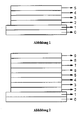
- a possibility of realization of an organic solar cell already proposed in the past consists in a pin diode ( K. Walze et al., Chem. Rev. 107, 1233, 2007 ), or a plurality of stacked pin diodes ( B. Mannig et al., Appl. Phys. A 79, 2004 ) with the following layer structure according to illustration 1 , or (Ex. Of a tandem solar cell) according to Figure, 2 ,
- the arrangement of the organic layers according to the pin concept between the electrodes is not limited to the above examples, but can be implemented inter alia with layer stacks of the geometry nip, pnip, pnipn, nipnip, etc.
- n or p denote an n- or p-doping of the respective layer, which leads to an increase in the density of free charge carriers in the thermal equilibrium state.
- charge carrier transport layers are primarily to be understood as charge carrier transport layers.
- doping of organic materials By adding an acceptor-like or donor-like dopant to organic matrix materials, the equilibrium charge carrier concentration in the layer is increased and the conductivity is increased.
- the doped layers are used as injection layers at the interface with the contact materials in electroluminescent devices. Similar Dotiezungsan accounts are analogously useful for solar cells.
- TCNQ Maitrot et al., J. Appl. Phys. 60, 2396, 1986
- F 4 -TCNQ M. Pfeffer et al., Appl. Phys. Lett. 73, 3202, 1998
- F 6 -TNAP PK Koech et al., Chem. Mater. 22, 3936, 2010
- BEDT-TTF A. Nollau et al., J. Appl. Phys. 87, 4340, 2000
- cationic dyes A. Werner et al., Appl. Phys. Lett.
- inorganic dopants such as WO 3 (US Pat. CC Chang et al., Appl. Phys. Lett. 89 (25), 253504, 2006 ), MoO 3 ( M. Kroger et al., Org. Electron. 10 (5), 932, 2009 ), Alkali metals ( J. Kido et al., Appl. Phys. Lett.
- Organic dopants or metal complex dopants are generally preferable to the use of inorganic dopants, such as lithium or cesium (n-type dopants), as they often readily diffuse in the device due to their small size, thus making it difficult to produce well-defined transitions between differently doped regions reduce the thermal stability of the device.
- one or more i-layers can consist both of successively deposited layers and of so-called interpetrating networks of several materials.
- the light incident through the transparent contact first generates excitons in the i-layer or in the n- / p-layer, ie electrically neutral excitation states (bound electron-hole pairs). These excitons can only be separated by very high electric fields or at suitable interfaces.
- sufficiently high fields are not available, so that all promising concepts for organic solar cells based on the exciton separation at the photoactive interfaces (organic donor-acceptor interface - CW Tang, Appl. Phys. Lett., 48 (2), 183, 1986 ) or at the interface of an organic to an inorganic semiconductor (cf.
- i-layer serves to protect the i-layer (s) from destructive influences during and after the deposition of contact layers or recombination zones. It is particularly advantageous if they only absorb in the UV or UV-near region of the visible solar spectrum. Thus, it is ensured that the substantial absorption takes place in the active i-layers and that no excitons are generated in regions which are farther away than the exciton-dendritic length from the separating interface. A parasitic absorption of visible light in the non-current generating areas of the solar cell is hereby prevented.
- the ETM should meet the above requirements to a sufficient extent in order to make the pin concept for organic solar cells feasible in full consequence. It should in addition to the usability in pin structures in particular also a feasibility of nip, min and tandem, triple or multiple cell structures by just this ETM are possible.
- PV-TPD N, N '- (4- (2,2-diphenyl-ethen-1-yl) -phenyl) -N, N'-di (4-methylphenylphenyl) benzidine
- di-NPB N, N'-bis (4- [N, N'-bis (naphth-1-yl) -amino] -biphenyl-4-yl) -benzidine
- the material NTCDA satisfies the requirements (1) to (3) with regard to the energetic properties: it is transparent with an optical energy gap of 3.05 eV, while the LUMO with approx. 4.0 eV at the level of the C 60 LUMOs lies ( C. Falkenberg et al., J. Appl. Phys.
- NTCDA NTCDA
- the extremely high roughness prevents the use of the material as a transparent intermediate layer, the so-called spacer, in tandem or triple solar cells.
- the material HATCN has a unusually high electron affinity, whereby an adjustment of the Elelctronentransporipractics to donor C 60 can not be guaranteed (point (2)), there is an injection barrier for electrons, which significantly affects the function of the corresponding pin solar cell and which only by the insertion of additional layers, ie by additional process steps, can be removed ( C. Falkenberg et al., Sol. Energ, Mat. Sol. C. 95, 927, 2011 ).
- the so-called pii structure is preferred to the pin structure.
- the n-doped electron transport layer is replaced by an undoped buffer layer, which protects the active intrinsic layers from the hot metal atoms of the cover clad.
- the transparent materials BPhen (bathophenanthroline) or BCP (bathocuproine) are used for this purpose, but they are not or only partially n-dopable due to their relatively low electron selectivity. Due to the low electronic conductivity or - mobility of these layers, these can be used only with small layer thicknesses of ⁇ 15 nm, otherwise they impede the injection of electrons ( MY Chan et al., J. Appl. Phys. 100, 094506, 2006 ; P. Peumans et al., J. Appl. Phys.
- the object of the invention is to provide an organic solar cell with improved electron transport material.
- the device is said to exhibit enhanced light absorption and, associated therewith, increased efficiency due to the improved properties of the electrosupport material over the prior art.
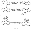
- this object is achieved by 2,7-bis (9 H -fluorene-2-yl) benzo [lmn] [3,8] phenanthroline-1,3,6,8 (2H, 7H) -tetrone compounds (5 ), here N, N-bis (fluoren-2-yl) -naphthalenetetracarboxydiimide (Bis-Fl-NTCDI), of the general formula ( Figure 3 ), where the radicals (R) represent atoms or atomic groups.
- NN-bis (fluorene-2-yl) -naphthalenetetracarboxydiimide compounds are provided, wherein R 1 -R 6 is independently selected from hydrogen, halogen, unsubstituted or substituted, saturated or unsaturated C 1 -C 20 alkyl, C 1 -C 20 -Reteroakl, C 1 -C 20 -alkenyl, C 1 -C 20 -Heteroalkenyl, C 1 -C 20 -alkynyl, C 1 -C 20 -Heteroalkinyl, C 6 -C 20 -aryl, C 6 -C 20 - Heteroaryl, saturated or unsaturated carbocyclic or heterocycle, which may be identical or different, where two adjacent radicals R 1 -R 6 may also be part of a further saturated or unsaturated, carbocyclic or heterocyclic ring, where the ring C, N, O, S, Si and Se may include.
- N, N-bis (fluoren-2-yl) naphthalenetetracarboxydimide compounds where R 1 -R 6 is independently selected from hydrogen, halogen, unsubstituted or substituted, saturated or unsaturated C 1 -C 3 -alkyl, C 1 - C 3 -Heteroalkyl, C 1 -C 3 -alkenyl, C 1 -C 3 -Heteroalkenyl, C 1 -C 3 -alkynyl, C 1 -C 3 -Heteroalkinyl, which may be identical or different, wherein two adjacent radicals R 1 R 6 may also be part of a further saturated or unsaturated, carbocyclic or heterocyclic ring, which ring may comprise C, N, O, S, Si and Se.
- N, N-bis (fluorene-2-yl) -naphthalenetetracarboxydimide compounds wherein R 1 -R 6 is independently selected from hydrogen, halo, C 1 -C 2 -heteroalkynyl, which may be the same or different.
- the Bis-Fl-NTCDI compounds according to the invention have not yet been described in the literature.
- some methods using high-boiling solvents such as dimethylformamide or diethylformamide
- high-boiling solvents such as dimethylformamide or diethylformamide
- zinc acetate as Promoter.
- the condensation of the fluoren-2-yl-amines to the bis-FI-NTCDI compounds was realized in low-boiling pyridine as a solvent, which results in a higher purity of the products ( Figure 4 ).
- the amines needed for the condensation were obtained directly from chemical surfactants or prepared in a two-step synthesis.
- 2-nitrofluorene is first alkylated at the bridging C9 carbon atom and then the nitrofunction is converted by hydrogenation into the corresponding fluoren-2-yl-amine.
- bis-RFl-NTCDI compounds 5b methyl, Me
- the use of the bis-F-L-NCDI compound in an organic solar cell as an exciton blocker and / or electron transport layer or as a conversion contact to an electrode within a p / n junction in a stacked organic solar cell.
- an organic compound comprising at least one organic matrix material which is doped with at least one dopant, wherein the matrix material is a Bis-Fl-NTCDI compound according to the invention.
- the bis-Fl-NTCDI compound is preferably n-doped, the doping techniques being known to the person skilled in the art.
- a p / n transition in an organic electronic component for connecting stacked organic solar cells or as a conversion contact to an electrode (“ Highly doped layers as efficient electron-hole recombination contacts for tandem organic solar cells ", R. Timmreck, J. Appl. Phys. 108, 033108, 2010 or EP1804308 ).
- Also contemplated by the present invention is a p / n junction in an organic electronic device that enhances the injection of charge carriers in the form of holes into a p-type organic semiconductor material layer, wherein the n-type organic semiconductor material layer includes a n-type organic semiconductor material Anode executed electrode is in contact.
- n-side transition comprises a bis-FI-NTCDI compound in an electron transport layer and / or a bis-FI-NTCDI compound in an intermediate layer between the p- and the n-side includes.
- n-side junction comprises a bis-ni-NTCDI compound in an electron transport layer and / or a thin metal layer in an intermediate layer between the p- and n-type layers.
- Page includes.
- the inventive bis-FI-NTCDI compounds can be used as Elekttonetransportmaterialien.
- metal complexes such as W 2 (hpp) 4 and also with cationic dyes (Acridine Orange Base)
- a significantly improved conductivity can be achieved.
- the enhanced electron transport layer is completely transparent in the visible region of the solar spectrum due to an optical band gap of> 3 eV.
- the inventively proposed bis-FI-NTCDI compounds have the potential to achieve a higher photocurrent density compared with the prior art and thus an increased power efficiency. Furthermore, an increased long-term stability could be detected.
- IR (ATR): ⁇ 3062 (w), 2960 (m), 2922 (m), 2854 (w), 1608 (w), 1589 (m), 1517 (m), 1465 (m), 1447 (m), 1396 (w), 1330 (s), 1264 (w), 1190 (w), 1128 (m), 1069 (m), 1038 (w), 900 (m), 839 (m), 771 (m), 754 (s), 736 (s), 650 (m), 601 (m), 559 (m).
- 2-nitro-9,9-dipropyl-9 H -fluorene (2d) An aqueous sodium hydroxide solution (13.0 mL, 50%) under water bath cooling to a solution of 2-nitro-9 H -fluorene (1, 6.34g, 30mmol) and tetrabutylammonium bromide (0.40g, 1.24mmol) in DMSO (100mL) and 1-bromopropane (13.6mL, 149mmol). The reaction mixture was stirred for 30 min and poured into 1 L of water. The mixture was extracted several times with dichloromethane, the combined organic phases dried over anhydrous sodium sulfate and concentrated.
- IR (ATR): v 30662 (w), 2958 (m), 2928 (m), 2873 (w), 2857 (w), 1609 (w), 1589 (m), 1559 (m), 1541 (w ), 1515 (m), 1468 (m), 1398 (w), 1375 (w), 1333 (s), 1247 (w), 1157 (w), 1129 (m), 1078 (m), 1049 (w ), 1026 (w), 904 (m), 876 (m), 836 (m), 769 (m), 736 (s), 638 (m), 589 (m), 558 (w).
- 9,9-dibutyl-2-nitro-9 H -fluorene (2e) An aqueous sodium hydroxide solution (20.9 mL, 50%) under water bath cooling to a solution of 2-nitro-9 H -fluorene (1, 10.55 g, 50 mmol) and tetrabutylammonium bromide (0.64 g, 2 mmol) in DMSO (200 mL) and butylbromide (26.8 mL, 250 mol). The reaction mixture was stirred for 30 min and poured into 1.8 L of water. The mixture was extracted several times with dichloromethane, the combined organic phases dried over anhydrous sodium sulfate and concentrated.
- IR (ATR): ⁇ 3061 (w), 2956 (m), 2927 (m), 2855 (m), 1608 (m), 1590 (m), 1559 (w), 1514 (m), 1463 (m ), 1397 (w), 1334 (s), 1304 (m), 1230 (w), 1158 (w), 1129 (m), 1077 (m), 1003 (w), 964 (w), 898 (m ), 837 (m), 777 (m), 738 (s), 632 (m), 596 (m), 570 (w).
- 9,9-Dimethyl-9 H -fluorene-2-amine (3b) 9,9-Dimethyl-2-nitro-9 H -fluorene ( 2b , 3.82 g, 15.97 mmol) was dissolved in ethanol (80 mL) and treated with hydrazine hydrate solution (2.3 mL, 47.3 mmol). After warming to 55-60 ° C, small portions of Raney nickel were added until the solution decolorized and all starting material was consumed as monitored by thin layer chromatography (hexanes / ethyl acetate (9: 1)). Thereafter, it was stirred for a further hour in the boiling heat and the catalyst was filtered off while hot. The solvent was removed by distillation and the residue recrystallized with hexane. The product 3b was obtained by filtration as a white powder (3.15 g, 15.05 mmol, 94%).
- 9,9-Diethyl-9 H -fluorene-2-amine (3c) 9,9-Diethyl-2-nitro-9 H -fluorene (2c) (7.51 g, 28.09 mmol) was dissolved in ethanol ( 100 mL) and treated with hydrazine hydrate solution (5 mL, 80%, 82.3 mmol). After warming to 55-60 ° C, small portions of Raney nickel were added until the solution decolorized and all the starting product was consumed as monitored by thin layer chromatography (hexanes / ethyl acetate (9: 1)). Thereafter, it was stirred for a further hour in the boiling heat and the catalyst was filtered off while hot. The solvent was removed by distillation and the residue recrystallized with hexane. The product 3c was obtained by filtration as a white powder (5.41 g, 22.79 mmol, 81%).
- IR (ATR): ⁇ 3420 (w), 3339 (w), 2957 (m), 2919 (w), 2870 (w), 1612 (w), 1582 (w), 1492 (w), 1449 (m ), 1372 (w), 1353 (w), 1326 (m), 1277 (m), 1210 (w), 1135 (w), 1021 (w), 923 (w), 871 (m), 860 (m ), 815 (m), 767 (s), 794 (m), 753 (m), 734 (s), 706 (m). 664 (s), 618 (s), 592 (m), 569 (s), 539 (s).
- 9,9-Dipropyl-9 H -fluoren-2-amine (3d) 9,9-Dipropyl-2-nitro-9 H -fluorene (2d) (6.52 g, 22.07 mmol) was dissolved in ethanol ( 120 mL) and treated with hydrazine hydrate solution (5.2 mL, 80%, 107 mmol). After warming to 55-60 ° C, small portions of Raney nickel were added until the solution decolorized and all starting material was consumed as monitored by thin layer chromatography (hexanes / ethyl acetate (9: 1)). Thereafter, it was stirred for a further hour in the boiling heat and the catalyst was filtered off while hot. The solvent was removed by distillation and the residue recrystallized with hexane. The product 3d was prepared by filtration as a white powder (5.39 g, 20.31 mmol, 92%).
- 9,9-Dibutyl-9 H -fluoren-2-amine (3e) 9,9-Dibutyl-2-nitro-9 H -fluorene (2a) (9.83 g, 30.39 mmol) was dissolved in ethanol ( 200 mL) and treated with hydrazine hydrate solution (4.7 mL, 80%, 77.4 mmol). After warming to 55-60 ° C, small portions of Raney nickel were added until the solution decolorized and all starting material was consumed as monitored by thin layer chromatography (hexanes / ethyl acetate (9: 1)). Thereafter, it was stirred for a further hour in the boiling heat and the catalyst was filtered off while hot. The solvent was removed by distillation and the residue was recrystallized with hexane. The product 3e was obtained by filtration as a white powder (7.99 g, 27.23 mmol, 90%).
- IR (ATR): ⁇ 3372 (w), 3058 (w), 2962 (w), 2919 (w), 2856 (w), 1743 (w), 1713 (m), 1671 (s), 1655 (m ), 1579 (m), 1447 (s), 1420 (m), 1334 (s), 1245 (s), 1192 (s), 1142 (w), 1115 (m), 1006 (w), 979 (m ), 939 (w), 880 (m), 830 (m), 783 (w), 761 (s), 739 (s), 626 (w), 588 (w), 568 (m).
- IR (ATR): ⁇ 3638 (w), 3077 (w), 2964 (w), 2918 (w), 2874 (w), 2853 (w), 1734 (w), 1715 (m), 1699 (m), 1974 (s), 1654 (m), 1636 (w), 1581 (m), 1487 (w), 1453 (m), 1420 (w), 1338 (s), 1246 (s), 1197 (m), 141 (w), 1118 (w), 1007 (w), 981 (m), 934 (w), 981 (w), 905 (w), 886 (w), 832 (w), 970 (m), 739 (s), 729 (s), 710 (w), 625 (m).
- IR (ATR): ⁇ 3663 (w), 3038 (m), 2955 (m), 2930 (w), 2869 (w), 2836 (w), 1714 (m), 1678 (s), 1654 (m ), 1580 (m), 1453 (m), 1336 (s), 1246 (s), 1211 (m), 1196 (m), 1118 (m), 1006 (w), 978 (m), 940 (m ), 885 (m), 838 (m), 784 (w), 768 (s), 743 (s), 652 (m), 588 (w).
- IR (ATR): ⁇ 3078 (w), 2954 (m), 2926 (m), 2858 (m), 1734 (w), 1715 (s), 1673 (s), 1654 (s), 1581 (m ), 1451 (m), 1338 (s), 1243 (s), 1198 (m), 1118 (w), 979 (m), 886 (m), 831 (m), 769 m), 739 (s) , 648 (w).
- bis-HFl-NTCDI N, N-bis (fluoren-2-yl) -naphthalenetetracarboxydiimide
- Figure 6 shows the absorption behavior of a vacuum deposited on a glass substrate thin film with a layer thickness of 65 nm.
- the optical band gap can be determined by the position of the absorption edge and results for bis-HFl-NTCDI to 3.02 eV, which is synonymous with the required transparency is in the visible range of the solar spectrum.
- An atomic force microscope (AFM) surface structure of a 65 nm thin vapor-deposited layer shows a very low mean square roughness (rms) of 2.4 nm (FIG. Figure 7 ). At room temperature (substrate) evaporated layers are therefore smooth and closed, which ensures a uniform growth of the subsequent layers.
- AFM atomic force microscope
- the material bis-BuFl-NTCDI was investigated by cyclic voltammetry in order to calculate the energy level of the LUMO and to prove the reversibility of the reduction process.
- Figure 8 shows two symmetrical peaks attributable to the first two reduction potentials.
- the ionization potential (E HOMO ) of a bis-F1-NTCDI thin film was determined by ultraviolet photoelectron spectroscopy (UPS).
- UPS ultraviolet photoelectron spectroscopy
- a 20 nm thin film Bis-Fl-NTCDI was deposited in a high vacuum on a freshly sputtered silver substrate. Subsequently, the sample was transferred into the measuring chamber without interruption of the vacuum.
- Figure 9 shows the resulting UP spectrum, from which the ionization potential can be calculated to be 6.55 eV.
- the aim is to demonstrate the dopability of bis-FI-NTCDI with known molecular n-dopants as well as the significant increase of the conductivity of doped thin films by means of transverse conductivity measurements.
- Bis-HFl-NTCDI was applied to a glass substrate coated with aluminum electrodes by co-evaporation with 7% (by weight) W 2 (hpp) 4. Already during the deposition process in a high vacuum, by applying a voltage between the Contact with a 2-point method then the current flowing are measured. From the geometry of the contacts and the layer thickness of the sample results in the conductivity of the doped material. How out Figure 10 can be seen, formed from a layer thickness of 3 nm of the organic semiconductor material closed percolation paths between the electrodes and it flows a measurable cross-flow. A completely closed layer is achieved at a film thickness of about 9 nm.
- the transverse conductivity of purified undoped organic materials is less than 10 -10 S cm -1 , while the above-described doping leads to an increase in the transverse conductivity to 1.1 10 -4 S cm -1 .
- the photoactive layers are formed from 5 nm zinc phthalocyanine (ZnPc), a 30 nm thick mixed layer of ZnPc and the fullerene C 60 in a mixing ratio of 1: 1 and a further 5 nm thick C 60 single layer. This is followed by a 50 nm thick n-doped electron transport layer of C 60 (3% w 2 (hpp) 4 ), or bis-HFl-NTCDI (7% W 2 (hpp) 4 ).
- the counter electrode is formed by a 100 nm thick aluminum layer. This layer sequence corresponds to a pin solar cell according to the current state of the art ( C. Falkenberg et al., J. Appl. Phys. 104 (3), 034506, 2008 ).
- the photoactive layers were formed by a 30 nm thick mixed layer of zinc phthalocyanine (ZnPc) and fullerene C 60 in a mixing ratio of 1: 1 and a further 30 nm thick C 60 single layer. This is followed by a 30 nm thick electron transport layer of bis-HFl-NTCDI, which is n-doped with 7% W 2 (hpp) 4 .
- the counter electrode is formed by a 100 nm thick aluminum layer.
- the finished device was encapsulated in a nitrogen atmosphere with a coverslip and aged at 50 ° C and illuminated with white LEDs at a power of 112 mW cm -2 .
- Figure 15 illustrates the development of efficiency over time. With an intensity of just under one sun, a decline in efficiency by 20 percentage points is registered after 18,000 h. As these are pure sunshine hours, the lifespan can be 80% of the initial efficiency at normal day-night rhythm can be extrapolated to approximately 18 years.
Applications Claiming Priority (1)
| Application Number | Priority Date | Filing Date | Title |
|---|---|---|---|
| DE102011013897A DE102011013897A1 (de) | 2011-03-11 | 2011-03-11 | Organische Solarzelle |
Publications (4)
| Publication Number | Publication Date |
|---|---|
| EP2498315A2 true EP2498315A2 (fr) | 2012-09-12 |
| EP2498315A3 EP2498315A3 (fr) | 2014-08-27 |
| EP2498315B1 EP2498315B1 (fr) | 2017-02-01 |
| EP2498315B8 EP2498315B8 (fr) | 2017-11-22 |
Family
ID=45952829
Family Applications (1)
| Application Number | Title | Priority Date | Filing Date |
|---|---|---|---|
| EP12001675.3A Active EP2498315B8 (fr) | 2011-03-11 | 2012-03-12 | Cellule solaire organique |
Country Status (2)
| Country | Link |
|---|---|
| EP (1) | EP2498315B8 (fr) |
| DE (1) | DE102011013897A1 (fr) |
Cited By (5)
| Publication number | Priority date | Publication date | Assignee | Title |
|---|---|---|---|---|
| WO2016156535A1 (fr) * | 2015-03-31 | 2016-10-06 | Sony Corporation | Matériaux actifs n et p pour couches organiques de conversion photoélectrique dans des photodiodes organiques. |
| CN110444673A (zh) * | 2019-08-27 | 2019-11-12 | 电子科技大学 | 一种基于无机化合物添加剂的有机薄膜太阳能电池及其制备方法 |
| WO2020020622A1 (fr) | 2018-07-24 | 2020-01-30 | Siemens Aktiengesellschaft | Cellule solaire à base de pérovskite organométallique, cellule solaire tandem et procédé de fabrication associé |
| WO2020020620A1 (fr) | 2018-07-24 | 2020-01-30 | Siemens Aktiengesellschaft | Cellule solaire à base de pérovskite organométallique, cellule solaire tandem et procédé de fabrication associé |
| CN111883665A (zh) * | 2020-08-28 | 2020-11-03 | 电子科技大学 | 一种通过在电荷传输层掺杂纳米粒子构建内部电场的有机太阳能电池及其制备方法 |
Families Citing this family (4)
| Publication number | Priority date | Publication date | Assignee | Title |
|---|---|---|---|---|
| US11545635B2 (en) | 2017-06-16 | 2023-01-03 | Ubiquitous Energy, Inc. | Visibly transparent, near-infrared-absorbing boron-containing photovoltaic devices |
| US10903438B2 (en) * | 2017-06-16 | 2021-01-26 | Ubiquitous Energy, Inc. | Visibly transparent, ultraviolet-absorbing photovoltaic devices |
| US11152581B2 (en) | 2017-06-16 | 2021-10-19 | Ubiquitous Energy, Inc. | Visibly transparent, near-infrared-absorbing donor/acceptor photovoltaic devices |
| US11778896B2 (en) | 2017-06-16 | 2023-10-03 | Ubiquitous Energy, Inc. | Visibly transparent, near-infrared-absorbing metal-complex photovoltaic devices |
Citations (5)
| Publication number | Priority date | Publication date | Assignee | Title |
|---|---|---|---|---|
| US5093698A (en) | 1991-02-12 | 1992-03-03 | Kabushiki Kaisha Toshiba | Organic electroluminescent device |
| DE10347856B4 (de) | 2003-10-10 | 2006-07-06 | Colorado State University Research Foundation, Fort Collins | Halbleiterdotierung |
| EP1804308A1 (fr) | 2005-12-23 | 2007-07-04 | Novaled AG | Dispositif organique émetteur de lumière ayant plusieurs unités électroluminescentes organiques empilées les unes sur les autres |
| EP1804309A1 (fr) | 2005-12-23 | 2007-07-04 | Novaled AG | Dispositif électronique avec une structure en couches de nature organique |
| WO2010057471A1 (fr) | 2008-11-19 | 2010-05-27 | Novaled Ag | Composés de chinoxaline et matériaux semi-conducteurs |
Family Cites Families (7)
| Publication number | Priority date | Publication date | Assignee | Title |
|---|---|---|---|---|
| WO2004083958A2 (fr) * | 2003-03-19 | 2004-09-30 | Technische Universität Dresden | Composant photo-actif presentant des couches organiques |
| US7422777B2 (en) * | 2005-11-22 | 2008-09-09 | Eastman Kodak Company | N,N′-dicycloalkyl-substituted naphthalene-based tetracarboxylic diimide compounds as n-type semiconductor materials for thin film transistors |
| US7569693B2 (en) * | 2006-06-12 | 2009-08-04 | Northwestern University | Naphthalene-based semiconductor materials and methods of preparing and use thereof |
| EP2072557A4 (fr) * | 2006-10-11 | 2010-04-14 | Toray Industries | Matériau organique donneur d'électrons pour dispositifs photovoltaïques, matériau et dispositifs photovoltaïques |
| US8309955B2 (en) * | 2008-01-07 | 2012-11-13 | The Johns Hopkins University | Devices having high dielectric constant, ionically-polarizable materials |
| WO2009147237A1 (fr) * | 2008-06-06 | 2009-12-10 | Basf Se | Dérivés chlorés d'acide naphtalènetétracarboxylique, leur préparation et leur utilisation dans des dispositifs électroniques organiques |
| FR2933238B1 (fr) * | 2008-06-27 | 2011-01-14 | Commissariat Energie Atomique | Nouveaux materiaux macromoleculaires semi-conducteurs organiques mesomorphes |
-
2011
- 2011-03-11 DE DE102011013897A patent/DE102011013897A1/de not_active Withdrawn
-
2012
- 2012-03-12 EP EP12001675.3A patent/EP2498315B8/fr active Active
Patent Citations (5)
| Publication number | Priority date | Publication date | Assignee | Title |
|---|---|---|---|---|
| US5093698A (en) | 1991-02-12 | 1992-03-03 | Kabushiki Kaisha Toshiba | Organic electroluminescent device |
| DE10347856B4 (de) | 2003-10-10 | 2006-07-06 | Colorado State University Research Foundation, Fort Collins | Halbleiterdotierung |
| EP1804308A1 (fr) | 2005-12-23 | 2007-07-04 | Novaled AG | Dispositif organique émetteur de lumière ayant plusieurs unités électroluminescentes organiques empilées les unes sur les autres |
| EP1804309A1 (fr) | 2005-12-23 | 2007-07-04 | Novaled AG | Dispositif électronique avec une structure en couches de nature organique |
| WO2010057471A1 (fr) | 2008-11-19 | 2010-05-27 | Novaled Ag | Composés de chinoxaline et matériaux semi-conducteurs |
Non-Patent Citations (29)
| Title |
|---|
| A. NOLLAU ET AL., J. APPL. PHYS., vol. 87, 2000, pages 4340 |
| A. WERNER ET AL., APPL. PHYS. LETT., vol. 82, 2003, pages 4495 |
| B. 0'REGAN ET AL., NATURE, vol. 353, 1991, pages 737 |
| B. MÄNNIG ET AL., APPL. PHYS. A, vol. 79, 2004 |
| B. MÄNNIG ET AL., APPL. PHYS. A: MATER. SCI. PROCESS., vol. 79, 2004, pages L |
| C. C. CHANG ET AL., APPL, PHYS. LETT., vol. 89, no. 25, 2006, pages 253504 |
| C. FALKENBERG ET AL., J. APPL. PHYS., vol. 104, 2008, pages 034506 |
| C. FALKENBERG ET AL., J. APPL. PHYS., vol. 104, no. 3, 2008, pages 034506 |
| C. FALKENBERG ET AL., PROC. SPIE 6999, 2008, pages 69990S |
| C. FALKENBERG ET AL., SOL. ENERG, MAT. SOL. C., vol. 95, 2011, pages 927 |
| C. K. CHAN ET AL., ADV. FUNCT. MATER., vol. 16, 2006, pages 831 |
| C. W. TANG ET AL., APPL. PHYS. LETT., vol. 48, 1986, pages 183 |
| C.W. TANG, APPL. PHYS. LETT., vol. 48, no. 2, 1986, pages 183 |
| F. LI ET AL., J. APPL. PHYS., vol. 100, 2006, pages 023716 |
| F. LI ET AL., J. PHYS. CHEM. B, vol. 108, 2004, pages 17076 |
| J. KIDO ET AL., APPL. PHYS. LETT., vol. 73, no. 20, 1998, pages 2866 |
| K. HARADA ET AL., PHYS. REV. LETT., vol. 94, no. 3, 2003, pages 036601 |
| K. WALZER ET AL., CHEM. REV., vol. 107, 2007, pages 1233 |
| M. KROGER ET AL., ORG. ELECTRON., vol. 10, no. 5, 2009, pages 932 |
| M. MAITROT ET AL., J. APPL. PHYS., vol. 60, 1986, pages 2396 |
| M. PFEIFFER ET AL., APPL. PHYS. LETT., vol. 73, 1998, pages 3202 |
| M. Y. CHAN ET AL., J. APPL. PHYS., vol. 100, 2006, pages 094506 |
| P. K. KOECH ET AL., CHEM MATER., vol. 22, 2010, pages 3936 |
| P. PEUMANS ET AL., J. APPL. PHYS., vol. 93, 2003, pages 3693 |
| R. SCHÜPPEL, J. APPL. PHYS., vol. 107, 2010, pages 044503 |
| R. TIMMRECK, J. APPL. PHYS., vol. 108, 2010, pages 033108 |
| R. TIMMRECK: "Highly doped layers as efficient electron-hole recombination contacts for tandem organic solar cells", J. APPL. PHYS., vol. 108, 2010, pages 033108 |
| S. PFÜTZNER ET AL.: "Characterisation of different hole transport materials as used in organic p-i-n solar cells", PROE. OF SPIE, vol. 6999, 2008, pages 69991M, XP008122340, DOI: doi:10.1117/12.782412 |
| T, AMERI ET AL., ENERG. ENVIRON. SCI, vol. 2, 2009, pages 347 |
Cited By (10)
| Publication number | Priority date | Publication date | Assignee | Title |
|---|---|---|---|---|
| WO2016156535A1 (fr) * | 2015-03-31 | 2016-10-06 | Sony Corporation | Matériaux actifs n et p pour couches organiques de conversion photoélectrique dans des photodiodes organiques. |
| KR20170128383A (ko) * | 2015-03-31 | 2017-11-22 | 소니 주식회사 | 유기 포토다이오드에서의 유기 광전 변환 층을 위한 n 및 p 활성 물질 |
| US20180123050A1 (en) * | 2015-03-31 | 2018-05-03 | Sony Corporation | N and p active materials for organic photoelectric conversion layers in organic photodiodes |
| JP2018513558A (ja) * | 2015-03-31 | 2018-05-24 | ソニー株式会社 | 有機フォトダイオード中の有機光電変換層のためのnおよびp活性材料 |
| US10790454B2 (en) | 2015-03-31 | 2020-09-29 | Sony Corporation | N and P active materials for organic photoelectric conversion layers in organic photodiodes |
| US11968895B2 (en) | 2015-03-31 | 2024-04-23 | Sony Corporation | N and P active materials for organic photoelectric conversion layers in organic photodiodes |
| WO2020020622A1 (fr) | 2018-07-24 | 2020-01-30 | Siemens Aktiengesellschaft | Cellule solaire à base de pérovskite organométallique, cellule solaire tandem et procédé de fabrication associé |
| WO2020020620A1 (fr) | 2018-07-24 | 2020-01-30 | Siemens Aktiengesellschaft | Cellule solaire à base de pérovskite organométallique, cellule solaire tandem et procédé de fabrication associé |
| CN110444673A (zh) * | 2019-08-27 | 2019-11-12 | 电子科技大学 | 一种基于无机化合物添加剂的有机薄膜太阳能电池及其制备方法 |
| CN111883665A (zh) * | 2020-08-28 | 2020-11-03 | 电子科技大学 | 一种通过在电荷传输层掺杂纳米粒子构建内部电场的有机太阳能电池及其制备方法 |
Also Published As
| Publication number | Publication date |
|---|---|
| DE102011013897A1 (de) | 2012-09-13 |
| EP2498315A3 (fr) | 2014-08-27 |
| EP2498315B8 (fr) | 2017-11-22 |
| EP2498315B1 (fr) | 2017-02-01 |
Similar Documents
| Publication | Publication Date | Title |
|---|---|---|
| EP2498315B1 (fr) | Cellule solaire organique | |
| EP0850492B1 (fr) | Cellule photovoltaique avec un compose spirannique | |
| EP0968507B1 (fr) | Cellule photovaltaique | |
| EP1861886B1 (fr) | Composant photoactif organique | |
| EP3050134B9 (fr) | Matériau organique photoactif pour composants optoélectroniques | |
| DE102010030500A1 (de) | Verdampfbares organisch halbleitendes Material und dessen Verwendung in einem optoelektronischen Bauelement | |
| WO2016102039A1 (fr) | Composés hétérocycliques à structures de dibenzazépine | |
| EP3519415A1 (fr) | Carbazoles comprenant des structures diazadibenzofurane ou diazadibenzothiophène | |
| WO2010075836A2 (fr) | Composés hétérocycliques et leur utilisation dans des composants électroniques et optoélectroniques | |
| EP3708634A1 (fr) | Composés spiraniques hétérocycliques | |
| EP2229699B1 (fr) | Complexes de dithiolène-métaux de transition, et composants électroniques ou optoélectroniques | |
| EP2976794B1 (fr) | Matériau organique photoactif pour composants optoélectroniques | |
| WO2016102040A1 (fr) | Carbazoles comportant deux substituants dibenzofuranne ou dibenzothiophène | |
| EP2867932B1 (fr) | Électrode transparente pour composants optoélectroniques | |
| WO2016045769A1 (fr) | Composés hétérocycliques à structures benzo [c] coumarine | |
| EP3044818B1 (fr) | Dispositif de l'électronique organique à couche active | |
| DE102009024956A1 (de) | Invertierte oder transparente organische Solarzelle oder Photodetektor mit verbesserter Absorption | |
| DE102012104247A1 (de) | Halbleitendes organisches Material für optoelektronische Bauelemente | |
| EP2659529B1 (fr) | Composant optoélectronique à couches dopées | |
| DE102015101835A1 (de) | Lichtabsorber | |
| DE102009022408A1 (de) | Organische Solarzelle oder Photodetektor mit verbesserter Absorption | |
| DE102022125417A1 (de) | Chemische Verbindung, optoelektronisches Bauelement mit mindestens einer solchen chemischen Verbindung, und Verwendung mindestens einer solchen chemischen Verbindung in einem optoelektronischen Bauelement | |
| DE102019118872A1 (de) | Organische Verbindung, und optoelektronisches Bauelement mit einer solchen organischen Verbindung |
Legal Events
| Date | Code | Title | Description |
|---|---|---|---|
| PUAI | Public reference made under article 153(3) epc to a published international application that has entered the european phase |
Free format text: ORIGINAL CODE: 0009012 |
|
| AK | Designated contracting states |
Kind code of ref document: A2 Designated state(s): AL AT BE BG CH CY CZ DE DK EE ES FI FR GB GR HR HU IE IS IT LI LT LU LV MC MK MT NL NO PL PT RO RS SE SI SK SM TR |
|
| AX | Request for extension of the european patent |
Extension state: BA ME |
|
| PUAL | Search report despatched |
Free format text: ORIGINAL CODE: 0009013 |
|
| AK | Designated contracting states |
Kind code of ref document: A3 Designated state(s): AL AT BE BG CH CY CZ DE DK EE ES FI FR GB GR HR HU IE IS IT LI LT LU LV MC MK MT NL NO PL PT RO RS SE SI SK SM TR |
|
| AX | Request for extension of the european patent |
Extension state: BA ME |
|
| RIC1 | Information provided on ipc code assigned before grant |
Ipc: H01L 51/46 20060101AFI20140723BHEP |
|
| 17P | Request for examination filed |
Effective date: 20140924 |
|
| RBV | Designated contracting states (corrected) |
Designated state(s): AL AT BE BG CH CY CZ DE DK EE ES FI FR GB GR HR HU IE IS IT LI LT LU LV MC MK MT NL NO PL PT RO RS SE SI SK SM TR |
|
| GRAP | Despatch of communication of intention to grant a patent |
Free format text: ORIGINAL CODE: EPIDOSNIGR1 |
|
| INTG | Intention to grant announced |
Effective date: 20160808 |
|
| RIN1 | Information on inventor provided before grant (corrected) |
Inventor name: HERMENAU, MARTIN Inventor name: LEO, KARL Inventor name: FALKENBERG, CHRISTIANE Inventor name: HUMMERT, MARKUS Inventor name: RIEDE, MORITZ, DR. Inventor name: OLTHOF, SELINA |
|
| GRAS | Grant fee paid |
Free format text: ORIGINAL CODE: EPIDOSNIGR3 |
|
| GRAA | (expected) grant |
Free format text: ORIGINAL CODE: 0009210 |
|
| AK | Designated contracting states |
Kind code of ref document: B1 Designated state(s): AL AT BE BG CH CY CZ DE DK EE ES FI FR GB GR HR HU IE IS IT LI LT LU LV MC MK MT NL NO PL PT RO RS SE SI SK SM TR |
|
| REG | Reference to a national code |
Ref country code: GB Ref legal event code: FG4D Free format text: NOT ENGLISH |
|
| REG | Reference to a national code |
Ref country code: CH Ref legal event code: EP Ref country code: AT Ref legal event code: REF Ref document number: 866226 Country of ref document: AT Kind code of ref document: T Effective date: 20170215 |
|
| REG | Reference to a national code |
Ref country code: IE Ref legal event code: FG4D Free format text: LANGUAGE OF EP DOCUMENT: GERMAN |
|
| REG | Reference to a national code |
Ref country code: DE Ref legal event code: R096 Ref document number: 502012009394 Country of ref document: DE |
|
| REG | Reference to a national code |
Ref country code: DE Ref legal event code: R081 Ref document number: 502012009394 Country of ref document: DE Owner name: NOVALED GMBH, DE Free format text: FORMER OWNER: TECHNISCHE UNIVERSITAET DRESDEN, 01069 DRESDEN, DE |
|
| REG | Reference to a national code |
Ref country code: NL Ref legal event code: MP Effective date: 20170201 |
|
| REG | Reference to a national code |
Ref country code: LT Ref legal event code: MG4D |
|
| PG25 | Lapsed in a contracting state [announced via postgrant information from national office to epo] |
Ref country code: LT Free format text: LAPSE BECAUSE OF FAILURE TO SUBMIT A TRANSLATION OF THE DESCRIPTION OR TO PAY THE FEE WITHIN THE PRESCRIBED TIME-LIMIT Effective date: 20170201 Ref country code: NO Free format text: LAPSE BECAUSE OF FAILURE TO SUBMIT A TRANSLATION OF THE DESCRIPTION OR TO PAY THE FEE WITHIN THE PRESCRIBED TIME-LIMIT Effective date: 20170501 Ref country code: GR Free format text: LAPSE BECAUSE OF FAILURE TO SUBMIT A TRANSLATION OF THE DESCRIPTION OR TO PAY THE FEE WITHIN THE PRESCRIBED TIME-LIMIT Effective date: 20170502 Ref country code: FI Free format text: LAPSE BECAUSE OF FAILURE TO SUBMIT A TRANSLATION OF THE DESCRIPTION OR TO PAY THE FEE WITHIN THE PRESCRIBED TIME-LIMIT Effective date: 20170201 Ref country code: IS Free format text: LAPSE BECAUSE OF FAILURE TO SUBMIT A TRANSLATION OF THE DESCRIPTION OR TO PAY THE FEE WITHIN THE PRESCRIBED TIME-LIMIT Effective date: 20170601 Ref country code: HR Free format text: LAPSE BECAUSE OF FAILURE TO SUBMIT A TRANSLATION OF THE DESCRIPTION OR TO PAY THE FEE WITHIN THE PRESCRIBED TIME-LIMIT Effective date: 20170201 |
|
| PG25 | Lapsed in a contracting state [announced via postgrant information from national office to epo] |
Ref country code: ES Free format text: LAPSE BECAUSE OF FAILURE TO SUBMIT A TRANSLATION OF THE DESCRIPTION OR TO PAY THE FEE WITHIN THE PRESCRIBED TIME-LIMIT Effective date: 20170201 Ref country code: PL Free format text: LAPSE BECAUSE OF FAILURE TO SUBMIT A TRANSLATION OF THE DESCRIPTION OR TO PAY THE FEE WITHIN THE PRESCRIBED TIME-LIMIT Effective date: 20170201 Ref country code: RS Free format text: LAPSE BECAUSE OF FAILURE TO SUBMIT A TRANSLATION OF THE DESCRIPTION OR TO PAY THE FEE WITHIN THE PRESCRIBED TIME-LIMIT Effective date: 20170201 Ref country code: SE Free format text: LAPSE BECAUSE OF FAILURE TO SUBMIT A TRANSLATION OF THE DESCRIPTION OR TO PAY THE FEE WITHIN THE PRESCRIBED TIME-LIMIT Effective date: 20170201 Ref country code: PT Free format text: LAPSE BECAUSE OF FAILURE TO SUBMIT A TRANSLATION OF THE DESCRIPTION OR TO PAY THE FEE WITHIN THE PRESCRIBED TIME-LIMIT Effective date: 20170601 Ref country code: NL Free format text: LAPSE BECAUSE OF FAILURE TO SUBMIT A TRANSLATION OF THE DESCRIPTION OR TO PAY THE FEE WITHIN THE PRESCRIBED TIME-LIMIT Effective date: 20170201 Ref country code: LV Free format text: LAPSE BECAUSE OF FAILURE TO SUBMIT A TRANSLATION OF THE DESCRIPTION OR TO PAY THE FEE WITHIN THE PRESCRIBED TIME-LIMIT Effective date: 20170201 Ref country code: BG Free format text: LAPSE BECAUSE OF FAILURE TO SUBMIT A TRANSLATION OF THE DESCRIPTION OR TO PAY THE FEE WITHIN THE PRESCRIBED TIME-LIMIT Effective date: 20170501 |
|
| RAP2 | Party data changed (patent owner data changed or rights of a patent transferred) |
Owner name: NOVALED GMBH |
|
| PG25 | Lapsed in a contracting state [announced via postgrant information from national office to epo] |
Ref country code: IT Free format text: LAPSE BECAUSE OF FAILURE TO SUBMIT A TRANSLATION OF THE DESCRIPTION OR TO PAY THE FEE WITHIN THE PRESCRIBED TIME-LIMIT Effective date: 20170201 Ref country code: SK Free format text: LAPSE BECAUSE OF FAILURE TO SUBMIT A TRANSLATION OF THE DESCRIPTION OR TO PAY THE FEE WITHIN THE PRESCRIBED TIME-LIMIT Effective date: 20170201 Ref country code: RO Free format text: LAPSE BECAUSE OF FAILURE TO SUBMIT A TRANSLATION OF THE DESCRIPTION OR TO PAY THE FEE WITHIN THE PRESCRIBED TIME-LIMIT Effective date: 20170201 Ref country code: EE Free format text: LAPSE BECAUSE OF FAILURE TO SUBMIT A TRANSLATION OF THE DESCRIPTION OR TO PAY THE FEE WITHIN THE PRESCRIBED TIME-LIMIT Effective date: 20170201 Ref country code: CZ Free format text: LAPSE BECAUSE OF FAILURE TO SUBMIT A TRANSLATION OF THE DESCRIPTION OR TO PAY THE FEE WITHIN THE PRESCRIBED TIME-LIMIT Effective date: 20170201 |
|
| REG | Reference to a national code |
Ref country code: CH Ref legal event code: PL |
|
| REG | Reference to a national code |
Ref country code: DE Ref legal event code: R097 Ref document number: 502012009394 Country of ref document: DE |
|
| PG25 | Lapsed in a contracting state [announced via postgrant information from national office to epo] |
Ref country code: DK Free format text: LAPSE BECAUSE OF FAILURE TO SUBMIT A TRANSLATION OF THE DESCRIPTION OR TO PAY THE FEE WITHIN THE PRESCRIBED TIME-LIMIT Effective date: 20170201 Ref country code: SM Free format text: LAPSE BECAUSE OF FAILURE TO SUBMIT A TRANSLATION OF THE DESCRIPTION OR TO PAY THE FEE WITHIN THE PRESCRIBED TIME-LIMIT Effective date: 20170201 Ref country code: MC Free format text: LAPSE BECAUSE OF FAILURE TO SUBMIT A TRANSLATION OF THE DESCRIPTION OR TO PAY THE FEE WITHIN THE PRESCRIBED TIME-LIMIT Effective date: 20170201 |
|
| PLBE | No opposition filed within time limit |
Free format text: ORIGINAL CODE: 0009261 |
|
| STAA | Information on the status of an ep patent application or granted ep patent |
Free format text: STATUS: NO OPPOSITION FILED WITHIN TIME LIMIT |
|
| REG | Reference to a national code |
Ref country code: IE Ref legal event code: MM4A |
|
| REG | Reference to a national code |
Ref country code: FR Ref legal event code: ST Effective date: 20171130 |
|
| 26N | No opposition filed |
Effective date: 20171103 |
|
| PG25 | Lapsed in a contracting state [announced via postgrant information from national office to epo] |
Ref country code: LU Free format text: LAPSE BECAUSE OF NON-PAYMENT OF DUE FEES Effective date: 20170312 Ref country code: FR Free format text: LAPSE BECAUSE OF NON-PAYMENT OF DUE FEES Effective date: 20170403 |
|
| PG25 | Lapsed in a contracting state [announced via postgrant information from national office to epo] |
Ref country code: LI Free format text: LAPSE BECAUSE OF NON-PAYMENT OF DUE FEES Effective date: 20170331 Ref country code: IE Free format text: LAPSE BECAUSE OF NON-PAYMENT OF DUE FEES Effective date: 20170312 Ref country code: SI Free format text: LAPSE BECAUSE OF FAILURE TO SUBMIT A TRANSLATION OF THE DESCRIPTION OR TO PAY THE FEE WITHIN THE PRESCRIBED TIME-LIMIT Effective date: 20170201 Ref country code: CH Free format text: LAPSE BECAUSE OF NON-PAYMENT OF DUE FEES Effective date: 20170331 |
|
| REG | Reference to a national code |
Ref country code: BE Ref legal event code: MM Effective date: 20170331 |
|
| REG | Reference to a national code |
Ref country code: AT Ref legal event code: MM01 Ref document number: 866226 Country of ref document: AT Kind code of ref document: T Effective date: 20170312 |
|
| PG25 | Lapsed in a contracting state [announced via postgrant information from national office to epo] |
Ref country code: BE Free format text: LAPSE BECAUSE OF NON-PAYMENT OF DUE FEES Effective date: 20170331 |
|
| PG25 | Lapsed in a contracting state [announced via postgrant information from national office to epo] |
Ref country code: AT Free format text: LAPSE BECAUSE OF NON-PAYMENT OF DUE FEES Effective date: 20170312 |
|
| PG25 | Lapsed in a contracting state [announced via postgrant information from national office to epo] |
Ref country code: MT Free format text: LAPSE BECAUSE OF FAILURE TO SUBMIT A TRANSLATION OF THE DESCRIPTION OR TO PAY THE FEE WITHIN THE PRESCRIBED TIME-LIMIT Effective date: 20170201 |
|
| PG25 | Lapsed in a contracting state [announced via postgrant information from national office to epo] |
Ref country code: HU Free format text: LAPSE BECAUSE OF FAILURE TO SUBMIT A TRANSLATION OF THE DESCRIPTION OR TO PAY THE FEE WITHIN THE PRESCRIBED TIME-LIMIT; INVALID AB INITIO Effective date: 20120312 |
|
| PG25 | Lapsed in a contracting state [announced via postgrant information from national office to epo] |
Ref country code: CY Free format text: LAPSE BECAUSE OF NON-PAYMENT OF DUE FEES Effective date: 20170201 |
|
| PG25 | Lapsed in a contracting state [announced via postgrant information from national office to epo] |
Ref country code: MK Free format text: LAPSE BECAUSE OF FAILURE TO SUBMIT A TRANSLATION OF THE DESCRIPTION OR TO PAY THE FEE WITHIN THE PRESCRIBED TIME-LIMIT Effective date: 20170201 |
|
| PG25 | Lapsed in a contracting state [announced via postgrant information from national office to epo] |
Ref country code: TR Free format text: LAPSE BECAUSE OF FAILURE TO SUBMIT A TRANSLATION OF THE DESCRIPTION OR TO PAY THE FEE WITHIN THE PRESCRIBED TIME-LIMIT Effective date: 20170201 |
|
| PG25 | Lapsed in a contracting state [announced via postgrant information from national office to epo] |
Ref country code: AL Free format text: LAPSE BECAUSE OF FAILURE TO SUBMIT A TRANSLATION OF THE DESCRIPTION OR TO PAY THE FEE WITHIN THE PRESCRIBED TIME-LIMIT Effective date: 20170201 |
|
| REG | Reference to a national code |
Ref country code: DE Ref legal event code: R079 Ref document number: 502012009394 Country of ref document: DE Free format text: PREVIOUS MAIN CLASS: H01L0051460000 Ipc: H10K0085000000 |
|
| P01 | Opt-out of the competence of the unified patent court (upc) registered |
Effective date: 20230515 |
|
| PGFP | Annual fee paid to national office [announced via postgrant information from national office to epo] |
Ref country code: DE Payment date: 20231229 Year of fee payment: 13 Ref country code: GB Payment date: 20240108 Year of fee payment: 13 |