EP2490208A1 - Display driving circuit, display device, and display driving method - Google Patents
Display driving circuit, display device, and display driving method Download PDFInfo
- Publication number
- EP2490208A1 EP2490208A1 EP10823222A EP10823222A EP2490208A1 EP 2490208 A1 EP2490208 A1 EP 2490208A1 EP 10823222 A EP10823222 A EP 10823222A EP 10823222 A EP10823222 A EP 10823222A EP 2490208 A1 EP2490208 A1 EP 2490208A1
- Authority
- EP
- European Patent Office
- Prior art keywords
- signal
- circuit
- polarity
- shift register
- electric potential
- Prior art date
- Legal status (The legal status is an assumption and is not a legal conclusion. Google has not performed a legal analysis and makes no representation as to the accuracy of the status listed.)
- Withdrawn
Links
Images




















Classifications
-
- G—PHYSICS
- G09—EDUCATION; CRYPTOGRAPHY; DISPLAY; ADVERTISING; SEALS
- G09G—ARRANGEMENTS OR CIRCUITS FOR CONTROL OF INDICATING DEVICES USING STATIC MEANS TO PRESENT VARIABLE INFORMATION
- G09G3/00—Control arrangements or circuits, of interest only in connection with visual indicators other than cathode-ray tubes
- G09G3/20—Control arrangements or circuits, of interest only in connection with visual indicators other than cathode-ray tubes for presentation of an assembly of a number of characters, e.g. a page, by composing the assembly by combination of individual elements arranged in a matrix no fixed position being assigned to or needed to be assigned to the individual characters or partial characters
- G09G3/34—Control arrangements or circuits, of interest only in connection with visual indicators other than cathode-ray tubes for presentation of an assembly of a number of characters, e.g. a page, by composing the assembly by combination of individual elements arranged in a matrix no fixed position being assigned to or needed to be assigned to the individual characters or partial characters by control of light from an independent source
- G09G3/36—Control arrangements or circuits, of interest only in connection with visual indicators other than cathode-ray tubes for presentation of an assembly of a number of characters, e.g. a page, by composing the assembly by combination of individual elements arranged in a matrix no fixed position being assigned to or needed to be assigned to the individual characters or partial characters by control of light from an independent source using liquid crystals
- G09G3/3611—Control of matrices with row and column drivers
- G09G3/3614—Control of polarity reversal in general
-
- G—PHYSICS
- G09—EDUCATION; CRYPTOGRAPHY; DISPLAY; ADVERTISING; SEALS
- G09G—ARRANGEMENTS OR CIRCUITS FOR CONTROL OF INDICATING DEVICES USING STATIC MEANS TO PRESENT VARIABLE INFORMATION
- G09G2300/00—Aspects of the constitution of display devices
- G09G2300/08—Active matrix structure, i.e. with use of active elements, inclusive of non-linear two terminal elements, in the pixels together with light emitting or modulating elements
- G09G2300/0876—Supplementary capacities in pixels having special driving circuits and electrodes instead of being connected to common electrode or ground; Use of additional capacitively coupled compensation electrodes
-
- G—PHYSICS
- G09—EDUCATION; CRYPTOGRAPHY; DISPLAY; ADVERTISING; SEALS
- G09G—ARRANGEMENTS OR CIRCUITS FOR CONTROL OF INDICATING DEVICES USING STATIC MEANS TO PRESENT VARIABLE INFORMATION
- G09G2310/00—Command of the display device
- G09G2310/02—Addressing, scanning or driving the display screen or processing steps related thereto
- G09G2310/0264—Details of driving circuits
-
- G—PHYSICS
- G09—EDUCATION; CRYPTOGRAPHY; DISPLAY; ADVERTISING; SEALS
- G09G—ARRANGEMENTS OR CIRCUITS FOR CONTROL OF INDICATING DEVICES USING STATIC MEANS TO PRESENT VARIABLE INFORMATION
- G09G2310/00—Command of the display device
- G09G2310/02—Addressing, scanning or driving the display screen or processing steps related thereto
- G09G2310/0264—Details of driving circuits
- G09G2310/0286—Details of a shift registers arranged for use in a driving circuit
-
- G—PHYSICS
- G09—EDUCATION; CRYPTOGRAPHY; DISPLAY; ADVERTISING; SEALS
- G09G—ARRANGEMENTS OR CIRCUITS FOR CONTROL OF INDICATING DEVICES USING STATIC MEANS TO PRESENT VARIABLE INFORMATION
- G09G2310/00—Command of the display device
- G09G2310/08—Details of timing specific for flat panels, other than clock recovery
-
- G—PHYSICS
- G09—EDUCATION; CRYPTOGRAPHY; DISPLAY; ADVERTISING; SEALS
- G09G—ARRANGEMENTS OR CIRCUITS FOR CONTROL OF INDICATING DEVICES USING STATIC MEANS TO PRESENT VARIABLE INFORMATION
- G09G2320/00—Control of display operating conditions
- G09G2320/02—Improving the quality of display appearance
- G09G2320/0219—Reducing feedthrough effects in active matrix panels, i.e. voltage changes on the scan electrode influencing the pixel voltage due to capacitive coupling
-
- G—PHYSICS
- G09—EDUCATION; CRYPTOGRAPHY; DISPLAY; ADVERTISING; SEALS
- G09G—ARRANGEMENTS OR CIRCUITS FOR CONTROL OF INDICATING DEVICES USING STATIC MEANS TO PRESENT VARIABLE INFORMATION
- G09G2320/00—Control of display operating conditions
- G09G2320/02—Improving the quality of display appearance
- G09G2320/0233—Improving the luminance or brightness uniformity across the screen
-
- G—PHYSICS
- G09—EDUCATION; CRYPTOGRAPHY; DISPLAY; ADVERTISING; SEALS
- G09G—ARRANGEMENTS OR CIRCUITS FOR CONTROL OF INDICATING DEVICES USING STATIC MEANS TO PRESENT VARIABLE INFORMATION
- G09G2340/00—Aspects of display data processing
- G09G2340/04—Changes in size, position or resolution of an image
- G09G2340/0407—Resolution change, inclusive of the use of different resolutions for different screen areas
-
- G—PHYSICS
- G09—EDUCATION; CRYPTOGRAPHY; DISPLAY; ADVERTISING; SEALS
- G09G—ARRANGEMENTS OR CIRCUITS FOR CONTROL OF INDICATING DEVICES USING STATIC MEANS TO PRESENT VARIABLE INFORMATION
- G09G3/00—Control arrangements or circuits, of interest only in connection with visual indicators other than cathode-ray tubes
- G09G3/20—Control arrangements or circuits, of interest only in connection with visual indicators other than cathode-ray tubes for presentation of an assembly of a number of characters, e.g. a page, by composing the assembly by combination of individual elements arranged in a matrix no fixed position being assigned to or needed to be assigned to the individual characters or partial characters
- G09G3/34—Control arrangements or circuits, of interest only in connection with visual indicators other than cathode-ray tubes for presentation of an assembly of a number of characters, e.g. a page, by composing the assembly by combination of individual elements arranged in a matrix no fixed position being assigned to or needed to be assigned to the individual characters or partial characters by control of light from an independent source
- G09G3/36—Control arrangements or circuits, of interest only in connection with visual indicators other than cathode-ray tubes for presentation of an assembly of a number of characters, e.g. a page, by composing the assembly by combination of individual elements arranged in a matrix no fixed position being assigned to or needed to be assigned to the individual characters or partial characters by control of light from an independent source using liquid crystals
- G09G3/3611—Control of matrices with row and column drivers
- G09G3/3648—Control of matrices with row and column drivers using an active matrix
- G09G3/3655—Details of drivers for counter electrodes, e.g. common electrodes for pixel capacitors or supplementary storage capacitors
-
- G—PHYSICS
- G09—EDUCATION; CRYPTOGRAPHY; DISPLAY; ADVERTISING; SEALS
- G09G—ARRANGEMENTS OR CIRCUITS FOR CONTROL OF INDICATING DEVICES USING STATIC MEANS TO PRESENT VARIABLE INFORMATION
- G09G3/00—Control arrangements or circuits, of interest only in connection with visual indicators other than cathode-ray tubes
- G09G3/20—Control arrangements or circuits, of interest only in connection with visual indicators other than cathode-ray tubes for presentation of an assembly of a number of characters, e.g. a page, by composing the assembly by combination of individual elements arranged in a matrix no fixed position being assigned to or needed to be assigned to the individual characters or partial characters
- G09G3/34—Control arrangements or circuits, of interest only in connection with visual indicators other than cathode-ray tubes for presentation of an assembly of a number of characters, e.g. a page, by composing the assembly by combination of individual elements arranged in a matrix no fixed position being assigned to or needed to be assigned to the individual characters or partial characters by control of light from an independent source
- G09G3/36—Control arrangements or circuits, of interest only in connection with visual indicators other than cathode-ray tubes for presentation of an assembly of a number of characters, e.g. a page, by composing the assembly by combination of individual elements arranged in a matrix no fixed position being assigned to or needed to be assigned to the individual characters or partial characters by control of light from an independent source using liquid crystals
- G09G3/3611—Control of matrices with row and column drivers
- G09G3/3674—Details of drivers for scan electrodes
-
- G—PHYSICS
- G09—EDUCATION; CRYPTOGRAPHY; DISPLAY; ADVERTISING; SEALS
- G09G—ARRANGEMENTS OR CIRCUITS FOR CONTROL OF INDICATING DEVICES USING STATIC MEANS TO PRESENT VARIABLE INFORMATION
- G09G3/00—Control arrangements or circuits, of interest only in connection with visual indicators other than cathode-ray tubes
- G09G3/20—Control arrangements or circuits, of interest only in connection with visual indicators other than cathode-ray tubes for presentation of an assembly of a number of characters, e.g. a page, by composing the assembly by combination of individual elements arranged in a matrix no fixed position being assigned to or needed to be assigned to the individual characters or partial characters
- G09G3/34—Control arrangements or circuits, of interest only in connection with visual indicators other than cathode-ray tubes for presentation of an assembly of a number of characters, e.g. a page, by composing the assembly by combination of individual elements arranged in a matrix no fixed position being assigned to or needed to be assigned to the individual characters or partial characters by control of light from an independent source
- G09G3/36—Control arrangements or circuits, of interest only in connection with visual indicators other than cathode-ray tubes for presentation of an assembly of a number of characters, e.g. a page, by composing the assembly by combination of individual elements arranged in a matrix no fixed position being assigned to or needed to be assigned to the individual characters or partial characters by control of light from an independent source using liquid crystals
- G09G3/3611—Control of matrices with row and column drivers
- G09G3/3674—Details of drivers for scan electrodes
- G09G3/3677—Details of drivers for scan electrodes suitable for active matrices only
Definitions
- the present invention relates to driving of display devices such as liquid crystal display devices having active-matrix liquid crystal display panels and, in particular, to a display driving circuit and a display driving method for driving a display panel in a display device employing a drive system referred to as CC (charge coupling) driving.
- CC charge coupling
- Patent Literature 1 A conventional CC driving system that is employed in an active-matrix liquid crystal display device is disclosed, for example, in Patent Literature 1. CC driving is explained by taking as an example the content of disclosure in Patent Literature 1.
- Fig. 57 shows a configuration of a device that realizes CC driving.
- Fig. 58 shows operating waveforms of various signals in CC driving of the device of Fig. 57 .
- the liquid crystal display device that carries out CC driving includes an image display section 110, a source line driving circuit 111, a gate line driving circuit 112, and a CS bus line driving circuit 113.
- the image display section 110 includes a plurality of source lines (signal lines) 101, a plurality of gate lines (scanning lines) 102, switching elements 103; pixel electrodes 104; a plurality of CS (capacity storage) bus lines (common electrode lines) 105, retention capacitors 106, liquid crystals 107, and a counter electrode 109.
- the switching elements 103 are disposed near points of intersection between the plurality of source lines 101 and the plurality of gate lines 102, respectively.
- the pixel electrodes 104 are connected to the switching elements 103, respectively.
- the CS bus lines 105 are paired with the gate lines 102, respectively, and arrange in parallel with one another.
- Each of the retention capacitors 106 has one end connected to a pixel electrode 104 and the other end connected to a CS bus line 105.
- the counter electrode 109 is provided in such a way as to face the pixel electrodes 104 with the liquid crystals 107 sandwiched therebetween.
- the source line driving circuit 111 is provided so as to drive the source lines 101
- the gate line driving circuit 112 is provided so as to drive the gate lines 102
- the CS bus line driving circuit 113 is provided so as to drive the CS bus lines 105.
- Each of the switching elements 103 is formed by amorphous silicon (a-Si), polycrystalline silicon (p-Si), monocrystalline silicon (c-Si), and the like. Because of such a structure, a capacitor 108 is formed between the gate and the drain of the switching element 103. This capacitor 108 causes a phenomenon in which a gate pulse from a gate line 102 shifts the electric potential of a pixel electrode 104 toward a negative side.
- the electric potential Vg of a gate line 102 in the liquid crystal display device is Von only during an H period (horizontal scanning period) in which the gate line 102 is selected, and retained at Voff during the other periods.
- the electric potential Vs of a source line 101 varies in amplitude depending on an video signal to be displayed, but takes a waveform that reverses its polarity every H period centered on the counter electrode potential Vcom and reverses its polarity in an adjacent H period concerning the same gate line 102 (line inversion driving). Since it is assumed in Fig. 58 that a uniform video signal is being inputted, the electric potential Vs changes with constant amplitude.
- the electric potential Vd of the pixel electrode 104 is equal to the electric potential Vs of the source line 101 because the switching element 103 conducts during a period in which the electric potential Vg is Von and, at the moment the electric potential Vg becomes Voff, the electric potential Vd shifts slightly toward a negative side through the gate-drain capacitor 108.
- the electric potential Vc of a CS bus line 105 is Ve+ during an H period in which the corresponding gate line 102 is selected and the next H period. Further, the electric potential Vc switches to Ve- during the H period after the next, and then retained at Ve- until the next field. This switching causes the electric potential Vd to be shifted toward a negative side through the retention capacitor 106.
- the electric potential Vd changes with larger amplitude than the electric potential Vs; therefore, the amplitude of change in the electric potential Vs can be made smaller. This allows achieving a simplification of circuitry and a reduction of power consumption in the source line driving circuit 111.
- the liquid crystal display device employing line inversion driving and CC driving has such a problem that in the first frame after the start of a display, there appear alternate bright and dark transverse stripes every single row (every single horizontal line of the liquid crystal display device).
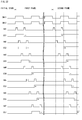
- Fig. 59 is a timing chart showing operation of the liquid crystal display device for explaining the cause of the problem.
- GSP is a gate start pulse that defines a timing of vertical scanning
- GCK1 (CK) and GCK2 (CKB) are gate clock signals that are outputted from the control circuit to define a timing of operation of the shift register.
- a period from a falling edge to the next falling edge in GSP corresponds to a single vertical scanning period (1V period).
- a period from a rising edge in GCK1 to a rising edge in GCK2 and a period from a rising edge in GCK2 to a rising edge in GCK1 each correspond to a single horizontal scanning period (1H period).
- CMI is a polarity signal that reverses its polarity every single horizontal scanning period.
- Fig. 59 shows the following signals in the order named: a source signal S (video signal), which is supplied from the source line driving circuit 111 to a source line 101 (source line 101 provided in the xth column); a gate signal G1, which is supplied from the gate line driving circuit 112 to a gate line 102 provided in the first row; a CS signal CS1, which is supplied from the bus line driving circuit 113 to a CS bus line 105 provided in the first row; and an electric potential Vpix1 of a pixel electrode provided in the first row and the xth column.
- a source signal S video signal
- G1 which is supplied from the gate line driving circuit 112 to a gate line 102 provided in the first row
- a CS signal CS1 which is supplied from the bus line driving circuit 113 to a CS bus line 105 provided in the first row
- an electric potential Vpix1 of a pixel electrode provided in the first row and the xth column.
- Fig. 59 shows the following signals in the order named: a gate signal G2, which is supplied to a gate line 102 provided in the second row; a CS signal CS2, which is supplied to a CS bus line 105 provided in the second row; and an electric potential Vpix2 of a pixel electrode provided in the second row and the xth column. Furthermore, Fig. 59 shows the following signals in the order named: a gate signal G3, which is supplied to a gate line 102 provided in the third row; a CS signal CS3, which is supplied to a CS bus line 105 provided in the third row; and an electric potential Vpix3 of a pixel electrode provided in the third row and the xth column.
- the start frame of a display picture is a first frame and that the first frame is preceded by an initial state.
- the source line driving circuit 111, the gate line driving circuit 112, and the CS bus line driving circuit 113 are all in the preparatory stages or in a resting state before entering into normal operation. Therefore, the gate signals G1, G2, and G3 are fixed at a gate-off potential (electric potential at which the gate of a switching element 103 is turned off), and the CS signals CS1, CS2, and CS3 are fixed at one electric potential (e.g., at a low level).
- the source line driving circuit 111, the gate line driving circuit 112, and the CS bus line driving circuit 113 are all in normal operation. This causes the source signal S to be a signal which has amplitude corresponding to a gray scale represented by a video signal and which reverses its polarity every 1H period.
- the gate signals G1, G2, and G3 serve as gate-on potentials (at which the gates of the switching elements 103 are turned on) during the first, second, and third 1H periods, respectively, in an active period (effective scanning period) of each frame, and serve as gate-off potentials during the other periods.
- the CS signals CS1, CS2, and CS3 are reversed after their corresponding gate signals G1, G2, and G3 fall, and take such waveforms that they are opposite in direction of reversal to one another.
- the CS signal CS2 rises after its corresponding gate signal G2 falls, and the CS signals CS1 1 and CS3 fall after their corresponding gate signals G1 and G3 fall.
- the CS signal CS2 falls after its corresponding gate signal G2 falls, and the CS signals CS1 and CS3 rise after their corresponding gate signals G1 and G3 fall.
- the relationship between rising and falling edges in the CS signals CS 1, CS2, and CS3 in the odd-numbered and even-numbered frames may be opposite of the relationship stated above.
- the timing of reversal of the CS signals CS1, CS2, and CS3 may be the falling edges in the gate signals G1, G2, and G3 or later, i.e., the corresponding horizontal scanning periods or later.
- the CS signals CS1, CS2, and CS3 may be reversed in synchronization with rising edges in gate signals in the next row.
- the CS signals CS1, CS2, and CS3 are all fixed at one electric potential (in Fig. 59 , at a low level) in the initial state, the electric potentials Vpix1 and Vpix3 are placed in an irregular state.
- the CS signal CS2 behaves in the same way as in the other odd-numbered frames (third, fifth frame, ...) in that it rises after the corresponding gate signal G2 falls, but the CS signals CS1 and CS3 behave differently from the other odd-numbered frames (third, fifth frame, ...) in that they are retained at the same electric potential (in Fig. 59 , at a low level) after the corresponding gate signals G1 and G3 fall.
- FIG. 60 is a block diagram showing a configuration of driving circuits (a gate line driving circuit 30 and a CS bus line driving circuit 40) shown in Patent Literature 2.
- Fig. 61 is a timing chart showing waveforms of various signals of a liquid crystal display device.
- Fig. 62 is a timing chart showing waveforms of various signals that are inputted to and outputted from the CS bus line driving circuit.
- the CS bus line driving circuit 40 has a plurality of CS circuits 41, 42, 43, ..., 4 n corresponding to their respective rows.
- the CS circuits 41, 42, 43, ..., 4 n include D latch circuits 41a, 42a, 43a, ..., 4na and OR circuits 41b, 42b, 43b, ..., 4 n b, respectively.
- the CS circuits 41 and 42 which correspond to the first and second rows respectively, are taken as an example.
- Input signals to the CS circuit 41 are the gate signals G1 and G2, a polarity signal POL, and a rest signal RESET, and input signals to the CS circuit 42 are the gate signals G2 and G3, the polarity signal POL, and the reset signal REST.
- the polarity signal POL and the reset signal RESET are inputted from the control circuit (not illustrated).
- the OR circuit 41b receives the gate signal G1 from the corresponding gate line 12 and the gate signal G2 from the gate line 12 of the next row and thereby outputs a signal g1 shown in Fig. 62 . Further, the OR circuit 42b receives the gate signal G2 from the corresponding gate line 12 and the gate signal G3 from the gate line 12 in the next row and thereby outputs a signal g2 shown in Fig. 62 .
- the D latch circuit 41a receives the reset signal RESET via its terminal CL, receives the polarity signal POL via its terminal D, and receives the output g1 via its clock terminal CK from the OR circuit 41b.
- the D latch circuit 41a outputs, as a CS signal CS1, an input state (low level or high level) of the polarity signal POL that it receives via its terminal D, and the CS signal CS1 indicates the change in electric potential level.
- the latch circuit 41a when the electric potential level of the signal g1 that the D latch circuit 41a receives via its clock terminal CK is a high level, the latch circuit 41a outputs an input state (low level or high level) of the polarity signal POL that it receives via its terminal D.
- the latch circuit 41a latches the input state (low level or high level) of the polarity signal POL that it received via its terminal D at the time of change, and keeps the latched state until the next time when the electric potential level of the signal g1 that the latch circuit 41a receives via its clock terminal CK is raised to a high level. Then, the D latch circuit 41a outputs the latched state as the CS signal CS1, shown in Fig. 62 , which indicates the change in electric potential level, via its terminal Q.
- the D latch circuit 42a receives the reset signal RESET via its terminal CL, receives the polarity signal POL via its terminal D, and receives the output g2 via its clock terminal CK from the OR circuit 42b. This allows the D latch circuit 42a to output a CS signal CS2, shown in Fig. 62 , which indicates a change in electric potential level, via its terminal Q.
- the foregoing configuration causes the CS signals CS1 and CS2 to be different in electric potential from each other at points in time where the gate signals in the first and second rows fall. Therefore, as shown in Fig. 61 , the electric potential Vpix1 is subjected to an electric potential shift caused by a change in electric potential of the CS signal CS 1, and the electric potential Vpix2 is subjected to an electric potential shift caused by a change in electric potential of the CS signal CS2. This allows eliminating such alternate bright and dark transverse stripes every single row as those shown in Fig. 59 .
- Patent Literature 2 is premised on line (1H) inversion driving by which the polarity of the voltage of a pixel electrode is reversed every single row (single line, single horizontal scanning period). That is, driving is carried out so that the electric potential of a CS signal varies every single line. Therefore, the electric potential of a CS signal cannot be made to vary, for example, every two rows. This causes such a problem that when this driving method is applied to a display device which carries out a display based on a video signal whose resolution has been converted to higher resolution (e.g., displays a double-size picture), there appear alternate bright and dark transverse stripes in a display picture.
- 1H line
- CS signal varies every single line. Therefore, the electric potential of a CS signal cannot be made to vary, for example, every two rows.
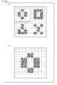
- Fig. 63 shows (i) display pictures displayed during normal driving and (ii) polarities of signal potentials supplied to pixel electrodes corresponding to the display pictures.
- (b) of Fig. 63 shows (i) the display picture shown in the upper left area (enclosed by a dotted line) in (a) of Fig. 63 and (ii) polarities of signal potentials supplied to the pixel electrodes as observed in a case where the resolution of the corresponding video signal has been converted by a factor of 2 both in the row-wise and column-wise directions (i.e., double-size display).
- the resolution conversion driving is carried out such that depending on the conversion factor, signals having the same polarity and the same electric potential (gray scale) are supplied to a plurality of pixels adjacent to each other in the column-wise direction (scanning direction).
- signals having the same polarity and the same electric potential (gray scale) are supplied to a plurality of pixels adjacent to each other in the column-wise direction (scanning direction).
- a source signal S supplied to the pixel electrode of the pixel located in the third row and the second column shown in (a) of Fig. 63 and (ii) a source signal S supplied to the pixel electrode of each of the pixels located in the fifth and sixth rows and the third and fourth columns shown in (b) of Fig. 63 are equal in polarity (which is here a negative polarity) and electric potential (gray scale) to each other.
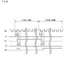
- Fig. 64 is a timing chart showing waveforms of various signals observed in a case where double-size display driving is employed in a conventional liquid crystal display device.
- Each of the reference signs "AA” to "SA” assigned to a source signal S shown in Fig. 64 corresponds to a single horizontal scanning period, and indicates a signal potential (gray scale) during that horizontal scanning period.
- the source signal S in the first frame exhibits identical signal potentials of a positive polarity ("AA") during the first and second horizontal scanning periods, and exhibits identical signal potentials of a negative polarity ("KA”) during the third and fourth horizontal scanning periods.
- AA positive polarity
- KA negative polarity
- the source signal S in the second frame exhibits identical signal potentials of a negative polarity ("II") during the first and second horizontal scanning periods, and exhibits identical signal potentials of a positive polarity ("KI") during the third and fourth horizontal scanning periods. Since polarities of voltages of pixel electrodes are reversed every two rows (two lines) like above in the case of the resolution conversion driving which realizes a double-size display, there appear alternate bright and dark transverse stripes (shaded areas in Fig. 64 ) in a display picture in a display device that employs line (1H) inversion driving.
- the above example is a case where the conversion factor is of a double size.
- the conversion factor is of a triple size or the resolution has been converted only in the column-wise direction, there will undesirably appear alternate bright and dark transverse stripes in a display picture.
- the present invention has been made in view of the problem, and an object of the present invention is to provide a display driving circuit and a display driving method each employing CC driving, which display driving circuit and display driving method are capable of improving display quality by eliminating appearance of alternate bright and dark transverse stripes that appear in a display picture when a display is carried out based on a video signal whose resolution has been converted to higher resolution.
- a display driving circuit in accordance with the present invention is a display driving circuit for use in a display device (i) which carries out a display based on a video signal whose resolution has been converted to higher resolution and (ii) in which by supplying retention capacitor wire signals to retention capacitor wires forming capacitors with pixel electrodes included in pixels, signal potentials written to the pixel electrodes from data signal lines are changed in a direction corresponding to polarities of the signal potentials, wherein, assuming that a direction in which scanning signal lines extend is a row-wise direction, when the resolution of the video signal is converted by a factor of n ( n is an integer of two or greater) at least in a column-wise direction, signal potentials having the same polarity and the same gray scale are supplied to pixel electrodes included in respective n pixels that correspond to n adjacent scanning signal lines and that are adjacent to each other in the column-wise direction, and a direction of change in the signal potentials written to the pixel electrodes from the data signal lines varies every n adjacent rows
- the display driving circuit signal potentials written to the pixel electrodes are changed, by the retention capacitor wire signals, in a direction corresponding to polarities of the signal potentials. This realizes CC driving. Further, according to the display driving circuit, a display is carried out based on a video signal whose resolution has been converted by a factor of n ( n is an integer of two or greater) at least in the column-wise direction. This realizes high-resolution conversion driving ( n- fold display driving).
- a direction of change in the signal potentials written to the pixel electrodes from the data signal lines varies every n adjacent rows according to the polarities of the signal potentials. For example, in a case of carrying out a display based on a video signal whose resolution has been converted by a factor of 2 (double-size display driving) in both the column-wise and row-wise directions, a direction of change in the signal potentials written to the pixel electrodes varies every two adjacent rows. This eliminates appearance of alternate bright and dark transverse stripes in a display picture (see Fig. 64 ). Accordingly, it is possible to eliminate appearance of alternate bright and dark transverse stripes in a display picture when a display device employing CC driving carries out high-resolution conversion driving (n-fold display driving), and thus possible to improve display quality of the display device.
- a display device in accordance with the present invention includes: any one of the foregoing display driving circuits; and a display panel.
- a display driving method in accordance with the present invention is a method for driving a display device (i) which carries out a display based on a video signal whose resolution has been converted to higher resolution and (ii) in which by supplying retention capacitor wire signals to retention capacitor wires forming capacitors with pixel electrodes included in pixels, signal potentials written to the pixel electrodes from data signal lines are changed in a direction corresponding to polarities of the signal potentials, said method including: when the resolution of the video signal is converted by a factor of n ( n is an integer of two or greater) at least in a column-wise direction, supplying signal potentials having the same polarity and the same gray scale to pixel electrodes included in respective n pixels that correspond to n adjacent scanning signal lines and that are adjacent to each other in the column-wise direction, assuming that a direction in which scanning signal lines extend is a row-wise direction; and causing a direction of change in the signal potentials written to the pixel electrodes from the data signal lines to vary every n adjacent rows
- the display driving method can bring about the same effects as those brought about by the configuration of the display driving circuit.
- a display driving circuit and a display driving method in accordance with the present invention are each configured such that, in a case where a display is carried out by CC driving based on a video signal whose resolution has been converted by a factor of n at least in a column-wise direction, a direction of change in signal potentials written to pixel electrodes from data signal lines varies every n adjacent rows depending on the polarities of the signal potentials.
- This allows a display device employing CC driving to eliminate appearance of alternate bright and dark transverse stripes that appear in a display picture when carrying out a display based on a video signal whose resolution has been converted by a factor of n, and to improve display quality.
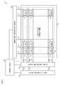
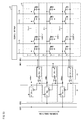
- Fig. 1 is a block diagram showing an overall configuration of the liquid crystal display device 1
- Fig. 2 is an equivalent circuit diagram showing an electrical configuration of each pixel of the liquid crystal display device 1.
- the liquid crystal display device 1 includes: an active-matrix liquid crystal display panel 10, which corresponds to a display panel of the present invention; a source bus line driving circuit 20, which corresponds to a data signal line driving circuit of the present invention; a gate line driving circuit 30, which corresponds to a scanning signal line driving circuit of the present invention; a CS bus line driving circuit 40, which corresponds to a retention capacitor wire driving circuit of the present invention; and a control circuit 50, which corresponds to a control circuit of the present invention.
- the liquid crystal display panel 10 constituted by sandwiching liquid crystals between an active matrix substrate and a counter substrate (not illustrated), has a large number of pixels P arranged in rows and columns.
- the liquid crystal display panel 10 includes: source bus lines 11, provided on the active matrix substrate, which correspond to data signal lines of the present invention; gate lines 12, provided on the active matrix substrate, which correspond to scanning signal lines of the present invention; thin-film transistors (hereinafter referred to as "TFTs") 13, provided on the active matrix substrate, which correspond to switching element of the present invention; pixel electrodes 14, provided on the active matrix substrate, which correspond to pixel electrodes of the present invention; CS bus lines 15, provided on the active matrix substrate, which correspond to retention capacitor wires of the present invention; and a counter electrode 19 provided on the counter substrate.
- TFTs 13 thin-film transistors 13
- pixel electrodes 14 provided on the active matrix substrate, which correspond to pixel electrodes of the present invention
- CS bus lines provided on the active matrix substrate, which correspond to retention capacitor wires of the present invention
- a counter electrode 19 provided on the counter substrate.
- the source bus lines 11 are arranged one by one in columns in parallel with one another along a column-wise direction (longitudinal direction), and the gate lines 12 are arranged one by one in rows in parallel with one another along a row-wise direction (transverse direction).
- the TFTs 13 are each provided in correspondence with a point of intersection between a source bus line 11 and a gate line 12, so are the pixel electrodes 14.
- Each of the TFTs 13 has its source electrode s connected to the source bus line 11, its gate electrode g connected to the gate line 12, and its drain electrode d connected to a pixel electrode 14.
- each of the pixel electrode 14 forms a liquid crystal capacitor 17 with the counter electrode 19 with liquid crystals sandwiched between the pixel electrode 14 and the counter electrode 19.
- the CS bus lines 15 are arranged one by one in rows in parallel with one another along a row-wise direction (transverse direction), in such a way as to be paired with the gate lines 12, respectively.
- the CS bus lines 15 each form a retention capacitor 16 (referred to also as "auxiliary capacitor") with each one of the pixel electrodes 14 arranged in each row, thereby being capacitively coupled to the pixel electrodes 14.
- the TFT 13 since, because of its structure, the TFT 13 has a pull-in capacitor 18 formed between the gate electrode g and the drain electrode d, the electric potential of the pixel electrode 14 is affected (pulled in) by a change in electric potential of the gate line 12. However, for simplification of explanation, such an effect is not taken into consideration here.
- the liquid crystal display panel 10 thus configured is driven by the source bus line driving circuit 20, the gate line driving circuit 30, and the CS bus line driving circuit 40. Further, the control circuit 50 supplies the source bus line driving circuit 20, the gate line driving circuit 30, and the CS bus line driving circuit 40 with various signals that are necessary for driving the liquid crystal display panel 10.
- each row is allotted a horizontal scanning period in sequence and scanned in sequence.
- the gate line driving circuit 30 sequentially outputs a gate signal for turning on the TFTs 13 to the gate line 12 in that row.
- the gate line driving circuit 30 will be described in detail later.
- the source bus line driving circuit 20 outputs a source signal to each source bus line 11. This source signal is obtained by the source bus line driving circuit 20 receiving a video signal from an outside of the liquid crystal display device 1 via the control circuit 50, allotting the video signal to each column, and giving the video signal a boost or the like.
- the source bus line driving circuit 20 is configured such that the polarity of the source signal it outputs is (i) identical for all pixels in an identical row and reversed every n adjacent lines and (ii) reversed in synchronization with vertical scanning periods.
- Fig. 4 which shows timings of 2-line (2H) inversion driving
- the polarity of a source signal S during the horizontal scanning periods in the first and second rows is reverse to the polarity of the source signal S during the horizontal scanning periods in the third and fourth rows.
- the polarity of the source signal S during the horizontal scanning period in the first row in the first frame is reverse to the polarity of the source signal S during the horizontal scanning period in the first row in the second frame. That is, in the case of the n-line (nH) inversion driving, the source signal S reverses its polarity (polarity of an electric potential of a pixel electrode) every n lines (n rows).
- the source bus line driving circuit 20 supplies signal potentials having the same polarity and the same gray scale every n rows ( n lines). For example, in a case of carrying out a display based on a video signal whose resolution as been converted by a factor of 2 in both the column-wise and row-wise directions, source signals S supplied to the first and second rows have the same voltage polarity and the same gray scale, whereas source signals S supplied to the third and fourth rows have the same voltage polarity and the same gray scale. It should be noted that although the following description assumes that one row (one line) corresponds to one horizontal scanning period, this does not imply any limitation on the present invention.
- the CS bus line driving circuit 40 outputs a CS signal corresponding to a retention capacitor wire signal of the present invention to each CS bus line 15.
- This CS signal is a signal whose electric potential switches (rises or falls) between two values (high and low electric potential levels), and is controlled such that the electric potential at a point in time where the TFTs 13 in the corresponding row are switched from on to off (i.e., at a point in time where the gate signal falls) varies every n adjacent lines.
- the CS bus line driving circuit 40 will be described in detail later.
- the control circuit 50 controls the gate line driving circuit 30, the source bus line driving circuit 20, and the CS bus line driving circuit 40, thereby causing each of them to output signals as shown in Fig. 4 .
- the liquid crystal display device having the above configuration is configured to (i) convert resolution of a video signal by a factor of n ( n is an integer of two or greater) at least in the column-wise direction and (ii) carry out n -line inversion driving.
- the liquid crystal display device in accordance with the present embodiment is configured to covert resolution of a video signal by a factor of n both in the column-wise and row-wise directions, this does not imply any limitation. Therefore, the liquid crystal display device can be configured to convert the resolution by a factor of n only in the column-wise direction.
- n-fold-size display driving is taken as an example.
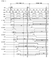
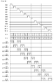
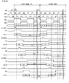
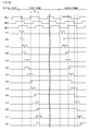
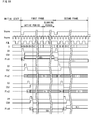
- Fig. 4 is a timing chart showing waveforms of various signals in a liquid crystal display device 1 that employs double-size display driving.
- GSP is a gate start pulse that defines a timing of vertical scanning
- GCK1 (CK) and GCK2 (CKB) are gate clocks that are outputted from the control circuit 50 to define a timing of operation of the shift register.
- a period from a falling edge to the next falling edge in GSP corresponds to a single vertical scanning period (1V period).
- a period from a rising edge in GCK1 to a rising edge in GCK2 and a period from a rising edge GCK2 to a rising edge in GCK1 each correspond to a single horizontal scanning period (1H period).
- CMI1 and CMI2 are each a polarity signal that reverses its polarity at predetermined timings.
- Fig. 4 shows the following signals in the order named: a source signal S (video signal), which is supplied from the source bus line driving circuit 20 to a source bus line 11 (source bus line 11 provided in the xth column); a gate signal G1, which is supplied from the gate line driving circuit 30 to a gate line 12 provided in the first row; a CS signal CS1, which is supplied from the bus line driving circuit 40 to a CS bus line 15 provided in the first row; and an electric potential waveform Vpix1 of a pixel electrode 14 provided in the first row and the xth column.
- a source signal S video signal
- Fig. 4 shows the following signals in the order named: a gate signal G2, which is supplied to a gate line 12 provided in the second row; a CS signal CS2, which is supplied to a CS bus line 15 provided in the second row; and an electric potential waveform Vpix2 of a pixel electrode 14 provided in the second row and the xth column.
- Fig. 4 shows the following signals in the order named: a gate signal G3, which is supplied to a gate line 12 provided in the third row; a CS signal CS3, which is supplied to a CS bus line 15 provided in the third row; and an electric potential waveform Vpix3 of a pixel electrode 14 provided in the third row and the xth column.
- Fig. 4 similarly shows a gate signal G4, a CS signal CS4, and an electric potential waveform Vpix4 in the order named and a gate signal G5, a CS signal CS5, and an electric potential waveform Vpix5 in the order named.
- the start frame of a display picture is a first frame and that the first frame is preceded by an initial state.
- the CS signals CS1 to CS5 are all fixed at one electric potential (in Fig. 4 , at a low level).
- the CS signal CS1 in the first row is at a high level at a point in time where the corresponding gate signals G1 (which corresponds to the output SRO1 from the corresponding shift register circuit SR1) falls.
- the CS signal CS2 in the second row is at a high level at a point in time where the corresponding gate signals G2 falls.
- the CS signal CS3 in the third row is at a low level at a point in time where the corresponding gate signals G3 falls.
- the CS signal CS4 in the fourth row is at a low level at a point in time where the corresponding gate signals G4 falls.
- the CS signal CS5 in the fifth row is at a high level at a point in time where the corresponding gate signals G5 falls.
- the source signal S is a signal which has amplitude corresponding to a gray scale represented by a video signal and which reverses its polarity every two horizontal scanning period (2H).
- the source signal S has the same electric potential (gray scale) during two adjacent horizontal scanning periods (2H) and has the same electric potential (gray scale) during next two adjacent horizontal scanning periods (2H). That is, each of the reference signs "AA” to "SA” shown in Fig. 4 corresponds to a single horizontal scanning period, and indicates a signal potential (gray scale) during that horizontal scanning period.
- the source signal S in the first frame exhibits identical signal potentials (gray scales) of a negative polarity ("AA”) during the first and second horizontal scanning periods, and exhibits identical signal potentials of a positive polarity ("KA”) during the third and fourth horizontal scanning periods.
- the source signal S in the second frame exhibits identical signal potentials of a positive polarity ("II") during the first and second horizontal scanning periods, and exhibits identical signal potentials of a negative polarity ("KI”) during the third and fourth horizontal scanning periods.
- the gate signals G1 to G5 serve as gate-on potentials during the first to fifth 1H periods, respectively, in an active period (effective scanning period) of each frame, and serve as gate-off potentials during the other periods.
- the CS signals CS1 to CS5 switch between high and low electric potential levels after their corresponding gate signals G1 to G5 fall.
- the CS signals CS1 and CS2 fall after their corresponding gate signals G1 and G2 fall, respectively, and the CS signals CS3 and CS4 rise after their corresponding signals G3 and G4 fall, respectively.
- this relationship is reversed, i.e., the CS signals CS1 and CS2 rise after their corresponding gate signals G1 and G2 fall, respectively, and the CS signals CS3 and CS4 fall after their corresponding gate signals G3 and G4 fall, respectively.
- the electric potential of each CS signal at a point in time where the gate signal falls varies every two rows in correspondence with the polarity of the source signal S; therefore, in the first frame, the electric potentials Vpix1 to Vpix5 of the pixel electrodes 14 are all properly shifted by the CS signals CS1 to CS5, respectively. Therefore, inputting of source signals S of the same gray scale causes the positive and negative electric potential differences between the electric potential of the counter electrode and the shifted electric potential of each of the pixel electrodes 14 to be equal to each other.
- the electric potentials of the CS signals corresponding to the first two rows are not polarity-reversed during the writing to the pixels corresponding to the first two rows, are polarity-reversed in a negative direction after the writing, and are not polarity-reversed until the next writing, and the electric potentials of the CS signals corresponding to the next two rows are not polarity-reversed during the writing to the pixels corresponding to the next two rows, are polarity-reversed in a positive direction after the writing, and are not polarity-reversed until the next writing.
- This realizes 2-line inversion driving in CC driving.
- the foregoing configuration allows the electric potentials Vpix1 to Vpix5 of the pixel electrodes 14 to be properly shifted by the CS signals CS1 to CS5, respectively, even in a case of double-size display driving (2-line inversion driving).
- This allows pixel electrodes 14 that are supplied with the same signal potential to be equal in electric potential to each other, thus making it possible to eliminate the appearance of transverse stripes shown in Fig. 64 .
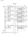
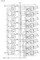
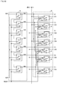
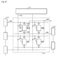
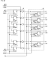
- Fig. 3 shows a configuration of the gate line driving circuit 30 and the CS bus line driving circuit 40.
- the CS bus line driving circuit 40 includes a plurality of CS circuits 41, 42, 43, ..., and 4 n corresponding to respective rows.
- the CS circuits 41, 42, 43, .., and 4 n include respective D latch circuits 41a, 42a, 43a, ..., and 4na; and respective OR circuits (logic circuits) 41b, 42b, 43b, ..., and 4nb.
- the gate line driving circuit 30 includes a plurality of shift register circuits SR1, SR2, SR3, ..., and SRn.
- gate line driving circuit 30 and the CS bus line driving circuit 40 are located on one side of a liquid crystal display panel in Fig. 3 , this does not imply any limitation.
- the gate line driving circuit 30 and the CS bus line driving circuit 40 may be located on respective different sides of the liquid crystal display panel.
- Input signals to the CS circuit 41 are shift register outputs SRO1 and SRO2 corresponding to respective gate signals G1 and G2, a polarity signal CMI1, and a reset signal RESET.
- Input signals to the CS circuit 42 are shift register outputs SRO2 and SRO3 corresponding to respective gate signals G2 and G3, a polarity signal CMI2, and the reset signal RESET.
- Input signals to the CS circuit 43 are shift register outputs SRO3 and SRO4 corresponding to respective gate signals G3 and G4, the polarity signal CMI1, and the reset signal RESET.
- Input signals to the CS circuit 44 are shift register outputs SRO4 and SRO5 corresponding to respective gate signals G4 and G5, the polarity signal CMI2, and the reset signal RESET.
- each CS circuit receives a shift register output SRO n in the corresponding n th row and a shift register output SRO n +1 in the next row, and receives one of the polarity signals CMI1 and CMI2 which alternate every row.
- the polarity signals CMI1 and CMI2 reverse their polarities every two horizontal scanning periods, and are out of phase with each other by one horizontal scanning period (refer to Fig. 4 ).
- the polarity signals CMI1 and CMI2 and the reset signal RESET are supplied from the control circuit 50.
- the D latch circuit 42a receives the reset signal RESET via its reset terminal CL, receives the polarity signal CMI2 (retention target signal) via its data terminal D (second input section), and receives an output from the OR circuit 42b via its clock terminal CK (first input section).
- the D latch circuit 42a outputs, as a CS signal CS2 indicative of the change in electric potential level, an input state (low level or high level) of the polarity signal CMI2 that it receives via its data terminal D.
- the D latch circuit 42a when the electric potential level of the signal that the D latch circuit 42a receives via its clock terminal CK is at a high level, the D latch circuit 42a outputs an input state (low level or high level) of the polarity signal CMI2 that it receives via its terminal D.
- the latch circuit 42a latches an input state (low level or high level) of the polarity signal CMI2 that it receives via its terminal D at the time of change, and keeps the latched state until the next time when the electric potential level of the signal that the latch circuit 42a receives via its clock terminal CK is raised to a high level. Then, the D latch circuit 42a outputs the CS signal CS2, which indicates the change in electric potential level, via its output terminal Q.
- the D latch circuit 43a receives the resent signal RESET via its reset terminal CL, and receives the polarity signal CMI1 via its data terminal D. Meanwhile, the D latch circuit 43a receives, via its clock terminal CK, an output from the OR circuit 43b. This causes the D latch circuit 43a to output a CS signal CS3, which indicates a change in electric potential level, via its output terminal Q (output section).
- the OR circuit 42b receives the output signal SRO2 from the shift resister circuit SR2 in its corresponding row and the output signal SRO3 from the shift register circuit SR3 in the next row and thereby outputs a signal M2 shown in Fig. 5 . Further, the OR circuit 43b receives the output signal SRO3 from the shift register circuit SR3 in its corresponding row and the output signal SRO4 from the shift register circuit SR4 in the next row and thereby outputs a signal M3 shown in Fig. 5 .
- a shift register output SRO supplied to each OR circuit is generated by a well-known method in the gate line driving circuit 30 (see Fig. 3 ) which includes D-type flip-flop circuits.
- the gate line driving circuit 30 sequentially shifts a gate start pulse GSP, which is supplied from the control circuit 50, to a shift register circuit SR in the next stage at a timing of the gate clock GCK having a frequency of one horizontal scanning period.
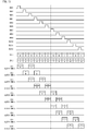
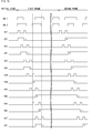
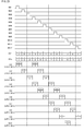
- Fig. 5 shows waveforms of various signals that are inputted to and outputted from the CS bus line driving circuit 40 of the liquid crystal display device 1 of Example 1.
- the D latch circuit 42a of the CS circuit 42 receives the polarity signal CMI2 via its terminal D and receives the reset signal RESET via its reset terminal CL.
- the reset signal RESET causes the electric potential of the CS signal CS2 that the D latch circuit 42a outputs via its output terminal Q to be retained at a low level.
- the shift register output SRO2 corresponding to the gate signal G2 to be supplied to the gate line 12 in the second row is outputted from the shift register circuit SR2, and is inputted to one terminal of the OR circuit 42b of the CS circuit 42. Then, a change (from low to high) in electric potential of the shift register output SRO2 in the signal M2 is inputted to the clock terminal CK.
- the D latch circuit 42a Upon receiving the change (from low to high) in electric potential of the shift register output SRO2 via its clock terminal CK, the D latch circuit 42a transfers an input state of the polarity signal CMI2 that it received via its data terminal D at the point in time, i.e., transfers a high level.
- the electric potential of the CS signal CS2 is switched from a low level to a high level at a time when there is a change (from low to high) in electric potential of the shift register output SRO2.
- the D latch circuit 42a outputs the high level until there is a change (from high to low) in electric potential of the shift register output SRO2 in the signal M2 inputted to the clock terminal CK (i.e., during a period of time in which the signal M2 is at a high level).
- the D latch circuit 42a latches an input state of the polarity signal CMI2 that it received at the point in time, i.e., latches a high level. After that, the D latch circuit 42a retains the high level until the signal M2 is raised to a high level.
- the shift register output SRO3 that has been shifted to the third row in the gate line driving circuit 30 is supplied to the other terminal of the OR circuit 42b.
- the shift register output SRO3 is supplied also to one terminal of the OR circuit 43b of the CS circuit 43.
- the D latch circuit 42a receives a change (from low to high) in electric potential of the shift register output SRO3 in the signal M2 via its clock terminal CK, and transfers an input state of the polarity signal CMI2 that it received via its terminal D at the point in time, i.e., transfers a low level. That is, the electric potential of the CS signal CS2 is switched from a high level to a low level at a time when there is a change (from low to high) in electric potential of the shift register output SRO3.
- the D latch circuit 42a outputs the low level until there is a change (from high to low) in electric potential of the shift register output SRO3 in the signal M2 inputted to the clock terminal CK (i.e., during a period of time in which the signal M2 is at a high level).
- the D latch circuit 42a latches an input state of the polarity signal CMI2 that it received at the point in time, i.e., latches a low level. After that, the D latch circuit 42a retains the low level until the signal M2 is raised to a high level in the second frame.
- the D latch circuit 42a transfers an input state (low level) of the polarity signal CMI2 that it received via its terminal D during a period of time in which the shift register output SRO2 in the signal M2 is at a high level, latches an input state (low level) of the polarity signal CMI2 that it received at a point in time where it received a change (from high to low) in electric potential of the shift register output SRO2, and then retains the low level until the next time the signal M2 is raised to a high level.
- the D latch circuit 42a transfers an input state of the polarity signal CMI2 that it received via its terminal D at the point in time, i.e., transfers a high level. That is, the electric potential of the CS signal CS2 is switched from a low level to a high level at a time when there is a change (from low to high) in electric potential of the shift register output SRO3.
- the D latch circuit 42a outputs the high level until there is a change (from high to low) in electric potential of the shift register output SRO3 inputted to the clock terminal CK (i.e., during a period of time in which the signal M2 is at a high level).
- the D latch circuit 42a latches an input state of the polarity signal CMI2 that it received at the point in time, i.e., latches a high level. After that, the D latch circuit 42a retains the high level until the signal M2 is raised to a high level in the third frame.
- the polarity signal CMI1 is latched in accordance with the shift register outputs SRO1 and SRO2, thereby a CS signal CS1 shown in Fig. 5 is outputted.
- the D latch circuit 43a of the CS circuit 43 receives the polarity signal CMI1 via its terminal D and receives the reset signal RESET via its reset terminal CL.
- the reset signal RESET causes the electric potential of the CS signal CS3 that the D latch circuit 43a outputs via its output terminal Q to be retained at a low level.
- the shift register output SRO3 corresponding to the gate signal G3 to be supplied to the gate line 12 in the third row is outputted from the shift register circuit SR3, and is inputted to one terminal of the OR circuit 43b of the CS circuit 43. Then, a change (from low to high) in electric potential of the shift register output SRO3 in the signal M3 is inputted to the clock terminal CK.
- the D latch circuit 43a transfers an input state of the polarity signal CMI1 that it received via its terminal D at the point in time, i.e., transfers a low level.
- the D latch circuit 43a outputs the low level until the next time when there is a change (from high to low) in electric potential of the shift register output SRO3 in the signal M3 inputted to the clock terminal CK (i.e., during a period of time in which the signal M3 is at a high level). Then, upon receiving a change (from high to low) in electric potential of the shift register output SRO3 in the signal M3 via its clock terminal CK, the D latch circuit 43a latches an input state of the polarity signal CMI1 that it received at the point in time, i.e., latches a low level. After that, the D latch circuit 43a retains the low level until the signal M3 is raised to a high level.
- the shift register output SRO4 that has been shifted to the fourth row in the gate line driving circuit 30 is supplied to the other terminal of the OR circuit 43b.
- the shift register output SRO4 is supplied also to one terminal of the OR circuit 44b of the CS circuit 44.
- the D latch circuit 43a receives a change (from low to high) in electric potential of the shift register output SRO4 in the signal M3 via its clock terminal CK, and transfers an input state of the polarity signal CMI1 that it received via its terminal D at the point in time, i.e., transfers a high level. That is, the electric potential of the CS signal CS3 is switched from a low level to a high level at a time when there is a change (from low to high) in electric potential of the shift register output SRO4.
- the D latch circuit 43a outputs the high level until there is a change (from high to low) in electric potential of the shift register output SRO4 in the signal M3 inputted to the clock terminal CK (i.e., during a period of time in which the signal M3 is at a high level).
- the D latch circuit 43a latches an input state of the polarity signal CMI1 that it received at the point in time, i.e., latches a high level. After that, the D latch circuit 43a retains the high level until the signal M3 is raised to a high level in the second frame.
- the D latch circuit 43a transfers an input state (high level) of the polarity signal CMI1 that it received via its terminal D during a period of time in which the shift register output SRO3 in the signal M3 is at a high level, latches an input state (high level) of the polarity signal CMI1 that it received at a point in time where it received a change (from high to low) in electric potential of the shift register output SRO3, and then retains the high level until the next time the signal M3 is raised to a high level.
- the D latch circuit 43a receives a change (from low to high) in electric potential of the shift register output SRO4 via its clock terminal CK, and transfers an input state of the polarity signal CMI1 that it received via its terminal D at the point in time, i.e., transfers a low level. That is, the electric potential of the CS signal CS3 is switched from a high level to a low level at a time when there is a change (from low to high) in electric potential of the shift register output SRO4.
- the D latch circuit 43a outputs the low level until the next time when there is a change (from high to low) in electric potential of the shift register output SRO4 inputted to the clock terminal CK (i.e., during a period of time in which the signal M3 is at a high level). Then, upon receiving a change (from high to low) in electric potential of the shift register output SRO4 via its clock terminal CK, the D latch circuit 43a latches an input state of the polarity signal CMI1 that it received at the point in time, i.e., latches a low level. After that, the D latch circuit 43a retains the low level until the signal M3 is raised to a high level in the third frame.
- the polarity signal CMI2 is latched in accordance with the shift register outputs SRO4 and SRO5, thereby a CS signal CS4 shown in Fig. 5 is outputted.
- each of the CS circuits 41, 42, 43, ..., and 4n corresponding to the respective rows makes it possible, in each frame in 2-line inversion driving, to switch the electric potential of a CS signal at a point in time where a gate signal in a corresponding row falls (at a point in time where a TFT 13 is switched from on to off) between high and low levels after the gate signal in this row falls.
- a CS signal CS n supplied to the CS bus line 15 in the n th row is generated by latching an electric potential level of the polarity signal CMI1 at a point in time where the gate signal G n in the n th row rises and an electric potential level of the polarity signal CMI1 at a point in time where the gate signal G( n +1) in the ( n +1)th row rises and (ii) a CS signal CS n +1 supplied to the CS bus line 15 in the ( n +1)th row is generated by latching an electric potential level of the polarity signal CMI2 at a point in time where the gate signal G( n +1) in the ( n +1)th row rises and an electric potential level of the polarity signal CMI2 at a point in time where the gate signal G( n +2) in the ( n +2)th row rises.
- a CS signal CSn+2 supplied to the CS bus line 15 in the ( n +2)th row is generated by latching an electric potential level of the polarity signal CMI1 at a point in time where the gate signal G( n +2) in the ( n +2)th row rises and an electric potential level of the polarity signal CMI1 at a point in time where the gate signal G( n +3) in the ( n +3)th row rises
- a CS signal CS n +3 supplied to the CS bus line 15 in the ( n +3)th row is generated by latching an electric potential level of the polarity signal CMI2 at a point in time where the gate signal G( n +3) in the ( n +3)th row rises and an electric potential level of the polarity signal CMI2 at a point in time where the gate signal G( n +4) in the ( n +4)th row rises.
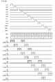
- Fig. 6 shows relations between (ii) the polarity signal CMI1 (or CMI2) and the shift register outputs SROn which are inputted to the CS circuits 4 n and (ii) the CS signals CS n outputted from the CS circuits 4 n .
- each of the sings A to L corresponds to a single horizontal scanning period, and indicates a polarity (positive polarity or negative polarity) during that horizontal scanning period.
- the CMI1 has a negative polarity during the second horizontal scanning period "B”
- each of the sings 1 to 12 corresponds to a single horizontal scanning period, and indicates a polarity during that horizontal scanning period.
- the CMI2 has a positive polarity during the first horizontal scanning period "1”, has a positive polarity during the second horizontal scanning period “2”, has a negative polarity during the third horizontal scanning period "3", and has a negative polarity during the fourth horizontal scanning period "4".
- the CMI1 and the CMI2 reverse their polarity every two horizontal scanning periods, and are out of phase with each other by one horizontal scanning period.
- Each of the CS circuits 4 n receives one of the polarity signals CMI1 and CMI2 which alternate every row.
- the CS circuit 41 receives the CMI1
- the CS circuit 42 receives the CMI2
- the CS circuit 43 receives the CMI1 (see Fig. 3 ).
- the CS circuit 4 n receives, via its clock terminal CK, a shift register output SRO n in the n th row and a shift register output SRO n +1 in the next ( n +1)th row. This causes the CS circuit 4n to latch (i) a CMI that the CS circuit 4 n receives via its data terminal D during the nth horizontal scanning period and (ii) a CMI that the CS circuit 4 n receives via its data terminal D during the ( n +1)th horizontal scanning period. For example, the CS circuit 41 loads a positive polarity of "A" of the CMI1 during the first horizontal scanning period, and loads a negative polarity of "B" of the CMI1 during the second horizontal scanning period.
- the CS circuit 42 loads a positive polarity of "2" of the CMI2 during the second horizontal scanning period, and loads a negative polarity of "3" of the CMI2 during the third horizontal scanning period.
- the CS circuit 43 loads a negative polarity of "C” of the CMI1 during the third horizontal scanning period, and loads a positive polarity of "D” of the CMI1 during the fourth horizontal scanning period.
- the CS circuit 44 loads a negative polarity of "4" of the CMI2 during the fourth horizontal scanning period, and loads a positive polarity of "5" of the CMI2 during the fifth horizontal scanning period. In this way, the CS signals CS n as shown in Figs. 4 and 5 are outputted.
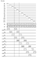
- Fig. 7 is a timing chart showing waveforms of various signals in triple-size display driving of the liquid crystal display device 1 shown in Fig. 3 .
- the CMI1 and CMI2 reverse their polarities at timings different from those in Fig. 4 .
- the CS signals CS1 to CS7 are all fixed at one electric potential (in Fig. 7 , at a low level).
- the CS signal CS1 in the first row is at a high level at a point in time where the corresponding gate signals G1 falls.
- the CS signal CS2 in the second row is at a high level at a point in time where the corresponding gate signals G2 falls.
- the CS signal CS3 in the third row is at a high level at a point in time where the corresponding gate signals G3 falls.
- the CS signal CS4 in the fourth row is at a low level at a point in time where the corresponding gate signals G4 falls
- the CS signal CS5 in the fifth row is at a low level at a point in time where the corresponding gate signals G5 falls
- the CS signal CS6 in the sixth row is at a low level at a point in time where the corresponding gate signals G6 falls.
- the CS signal CS7 in the seventh row is at a high level at a point in time where the corresponding gate signals G7 falls.
- the source signal S is a signal which has amplitude corresponding to a gray scale represented by a video signal and which reverses its polarity every three horizontal scanning period (3H).
- the source signal S has the same electric potential during three adjacent horizontal scanning periods (3H) and has the same electric potential during next three adjacent horizontal scanning periods (3H). That is, each of the reference signs "AA” to "SA” shown in Fig. 7 corresponds to a single horizontal scanning period, and indicates a signal potential (gray scale) during that horizontal scanning period.
- the source signal S in the first frame exhibits identical signal potentials of a negative polarity ("AA") during the first, second and third horizontal scanning periods, and exhibits identical signal potentials of a positive polarity ("KA") during the fourth, fifth and sixth horizontal scanning periods.
- the source signal S in the second frame exhibits identical signal potentials of a positive polarity ("II") during the first, second and third horizontal scanning periods, and exhibits identical signal potentials of a negative polarity ("KI”) during the fourth, fifth and sixth horizontal scanning periods.
- the gate signals G1 to G7 serve as gate-on potentials during the first to seventh 1H periods, respectively, in an active period (effective scanning period) of each frame, and serve as gate-off potentials during the other periods.
- the CS signals CS1 to CS7 switch between high and low electric potential levels after their corresponding gate signals G1 to G7 fall. Specifically, in the first frame, the CS signals CS1, CS2 and CS3 fall after their corresponding gate signals G1, G2 and G3 fall, respectively, and the CS signals CS4, CS5 and CS6 rise after their corresponding signals G4, G5 and G6 fall, respectively.
- the electric potential of each CS signal at a point in time where the gate signal falls varies every three rows in correspondence with the polarity of the source signal S; therefore, in the first frame, the electric potentials Vpix1 to Vpix7 of the pixel electrodes 14 are all properly shifted by the CS signals CS1 to CS7, respectively. Therefore, inputting of source signals S of the same gray scale causes the positive and negative electric potential differences between the electric potential of the counter electrode and the shifted electric potential of each of the pixel electrodes 14 to be equal to each other.
- the electric potentials of the CS signals corresponding to the first three rows are not polarity-reversed during the writing to the pixels corresponding to the first three rows, are polarity-reversed in a negative direction after the writing, and are not polarity-reversed until the next writing, and the electric potentials of the CS signals corresponding to the next three rows are not polarity-reversed during the writing to the pixels corresponding to the next three rows, are polarity-reversed in a positive direction after the writing, and are not polarity-reversed until the next writing.
- This realizes 3-line inversion driving in CC driving.
- the foregoing configuration allows the electric potentials Vpix1 to Vpix7 of the pixel electrodes 14 to be properly shifted by the CS signals CS1 to CS7, respectively, even in a case of triple-size display driving (3-line inversion driving).
- This allows pixel electrodes 14 that are supplied with the same signal potential to be equal in electric potential to each other, thus making it possible to eliminate the appearance of transverse stripes shown in Fig. 64 . As a result, it is possible to improve display quality.
- the polarity signals CMI1 and CMI2 reverse their polarity at timings different from those in Example 1.
- the other configurations are the same as those shown in Fig. 3 .
- Each CS circuit receives a shift register output SROn in the corresponding nth row and a shift register output SROn+1 in the next row, and receives one of the polarity signals CMI1 and CMI2 which alternate every row.
- the polarity signals CMI1 and CMI2 are set so as to reverse their polarities at the timings shown in Fig. 7 .
- Figs. 7 and 8 show the liquid crystal display device 1 which employs triple-size display driving.
- descriptions of connections in the gate line driving circuit 30 and the CS bus line driving circuit 40 are omitted.
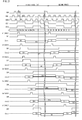
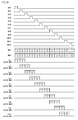
- Fig. 8 shows waveforms of various signals inputted to and outputted from the CS bus line driving circuit 40 of the liquid crystal display device 1 of Example 2.
- operations in the first frame are explained by taking as an example the CS circuits 42, 43 and 44 corresponding to the second, third and fourth rows, respectively.
- the D latch circuit 42a of the CS circuit 42 receives the polarity signal CMI2 via its terminal D and receives the reset signal RESET via its reset terminal CL.
- the reset signal RESET causes the electric potential of the CS signal CS2 that the D latch circuit 42a outputs via its output terminal Q to be retained at a low level.
- the shift register output SRO2 corresponding to the gate signal G2 to be supplied to the gate line 12 in the second row is outputted from the shift register circuit SR2, and is inputted to one terminal of the OR circuit 42b of the CS circuit 42. Then, a change (from low to high) in electric potential of the shift register output SRO2 in the signal M2 is inputted to the clock terminal CK.
- the D latch circuit 42a Upon receiving the change (from low to high) in electric potential of the shift register output SRO2 via its clock terminal CK, the D latch circuit 42a transfers an input state of the polarity signal CMI2 that it received via its data terminal D at the point in time, i.e., transfers a high level.
- the electric potential of the CS signal CS2 is switched from a low level to a high level at a time when there is a change (from low to high) in electric potential of the shift register output SRO2.
- the D latch circuit 42a outputs the high level until there is a change (from high to low) in electric potential of the shift register output SRO2 in the signal M2 inputted to the clock terminal CK (i.e., during a period of time in which the signal M2 is at a high level).
- the D latch circuit 42a latches an input state of the polarity signal CMI2 that it received at the point in time, i.e., latches a high level. After that, the D latch circuit 42a retains the high level until the signal M2 is raised to a high level.
- the shift register output SRO3 that has been shifted to the third row in the gate line driving circuit 30 is supplied to the other terminal of the OR circuit 42b.
- the shift register output SRO3 is supplied also to one terminal of the OR circuit 43b of the CS circuit 43.
- the D latch circuit 42a receives a change (from low to high) in electric potential of the shift register output SRO3 in the signal M2 via its clock terminal CK, and transfers an input state of the polarity signal CMI2 that it received via its terminal D at the point in time, i.e., transfers a low level. That is, the electric potential of the CS signal CS2 is switched from a high level to a low level at a time when there is a change (from low to high) in electric potential of the shift register output SRO3.
- the D latch circuit 42a outputs the low level until there is a change (from high to low) in electric potential of the shift register output SRO3 in the signal M2 inputted to the clock terminal CK (i.e., during a period of time in which the signal M2 is at a high level).
- the D latch circuit 42a latches an input state of the polarity signal CMI2 that it received at the point in time, i.e., latches a low level. After that, the D latch circuit 42a retains the low level until the signal M2 is raised to a high level in the second frame.
- the D latch circuit 42a transfers an input state (low level) of the polarity signal CMI2 that it received via its data terminal D during a period of time in which the shift register output SRO2 in the signal M2 is at a high level, latches an input state (low level) of the polarity signal CMI2 that it received at a point in time where it received a change (from high to low) in electric potential of the shift register output SRO2, and then retains the low level until the next time the signal M2 is raised to a high level.
- the D latch circuit 42a transfers an input state of the polarity signal CMI2 that it received via its data terminal D at the point in time, i.e., transfers a high level. That is, the electric potential of the CS signal CS2 is switched from a low level to a high level at a time when there is a change (from low to high) in electric potential of the shift register output SRO3.
- the D latch circuit 42a outputs the high level until there is a change (from high to low) in electric potential of the shift register output SRO3 inputted to the clock terminal CK (i.e., during a period of time in which the signal M2 is at a high level). Then, upon receiving a change (from high to low) in electric potential of the shift register output SRO2 via its clock terminal CK, the D latch circuit 42a latches an input state of the polarity signal CMI2 that it received at the point in time, i.e., latches a high level. After that, the D latch circuit 42a retains the high level until the signal M2 is raised to a high level in the third frame.
- the polarity signal CMI1 is latched in accordance with the shift register outputs SRO1 and SRO2, thereby a CS signal CS1 shown in Fig. 8 is outputted.
- the D latch circuit 43a of the CS circuit 43 receives the polarity signal CMI1 via its terminal D and receives the reset signal RESET via its reset terminal CL.
- the reset signal RESET causes the electric potential of the CS signal CS3 that the D latch circuit 43a outputs via its output terminal Q to be retained at a low level.
- the shift register output SRO3 corresponding to the gate signal G3 to be supplied to the gate line 12 in the third row is outputted from the shift register circuit SR3, and is inputted to one terminal of the OR circuit 43b of the CS circuit 43. Then, a change (from low to high) in electric potential of the shift register output SRO3 in the signal M3 is inputted to the clock terminal CK.
- the D latch circuit 43a transfers an input state of the polarity signal CMI1 that it received via its terminal D at the point in time, i.e., transfers a high level.
- the electric potential of the CS signal CS3 is switched from a low level to a high level at a time when there is a change (low to high) in electric potential of the shift register output SRO3. Then, the D latch circuit 43a outputs the high level until there is a change (from high to low) in electric potential of the shift register output SRO3 in the signal M3 inputted to the clock terminal CK (i.e., during a period of time in which the signal M3 is at a high level).
- the D latch circuit 43a latches an input state of the polarity signal CMI1 that it received at the point in time, i.e., latches a high level. After that, the D latch circuit 43a retains the high level until the signal M3 is raised to a high level.
- the shift register output SRO4 that has been shifted to the fourth row in the gate line driving circuit 30 is supplied to the other terminal of the OR circuit 43b.
- the shift register output SRO4 is supplied also to one terminal of the OR circuit 43b of the CS circuit 43.
- the D latch circuit 43a receives a change (from low to high) in electric potential of the shift register output SRO4 in the signal M3 via its clock terminal CK, and transfers an input state of the polarity signal CMI1 that it received via its terminal D at the point in time, i.e., transfers a low level. That is, the electric potential of the CS signal CS3 is switched from a high level to a low level at a time when there is a change (from low to high) in electric potential of the shift register output SRO4.
- the D latch circuit 43a outputs the low level until there is a change (from high to low) in electric potential of the shift register output SRO4 in the signal M3 inputted to the clock terminal CK (i.e., during a period of time in which the signal M3 is at a high level).
- the D latch circuit 43a latches an input state of the polarity signal CMI1 that it received at the point in time, i.e., latches a low level. After that, the D latch circuit 43a retains the low level until the signal M3 is raised to a high level in the second frame.
- the D latch circuit 43a transfers an input state (low level) of the polarity signal CMI1 that it received via its data terminal D during a period of time in which the shift register output SRO3 in the signal M3 is at a high level, latches an input state (low level) of the polarity signal CMI1 that it received at a point in time where it received a change (from high to low) in electric potential of the shift register output SRO3, and then retains the low level until the next time the signal M3 is raised to a high level.
- the D latch circuit 43a transfers an input state of the polarity signal CMI1 that it received via its data terminal D at the point in time, i.e., transfers a high level. That is, the electric potential of the CS signal CS3 is switched from a low level to a high level at a time when there is a change (from low to high) in electric potential of the shift register output SRO3.
- the D latch circuit 43a outputs the high level until there is a change (from high to low) in electric potential of the shift register output SRO4 inputted to the clock terminal CK (i.e., during a period of time in which the signal M3 is at a high level). Then, upon receiving a change (from high to low) in electric potential of the shift register output SRO3 via its clock terminal CK, the D latch circuit 43a latches an input state of the polarity signal CMI1 that it received at the point in time, i.e., latches a high level. After that, the D latch circuit 43a retains the high level until the signal M3 is raised to a high level in the third frame.
- the D latch circuit 44a of the CS circuit 44 receives the polarity signal CMI2 via its terminal D and receives the reset signal RESET via its reset terminal CL.
- the reset signal RESET causes the electric potential of the CS signal CS4 that the D latch circuit 44a outputs via its output terminal Q to be retained at a low level.
- the shift register output SRO4 for the fourth row is outputted from the shift register circuit SR4, and is inputted to one terminal of the OR circuit 44b of the CS circuit 44. Then, a change (from low to high) in electric potential of the shift register output SRO4 in the signal M4 is inputted to the clock terminal CK.
- the D latch circuit 44a Upon receiving the change (from low to high) in electric potential of the shift register output SRO4 via its clock terminal CK, the D latch circuit 44a transfers an input state of the polarity signal CMI2 that it received via its data terminal D at the point in time, i.e., transfers a low level.
- the D latch circuit 44a outputs the low level until there is a change (from high to low) in electric potential of the shift register output SRO4 in the signal M4 inputted to the clock terminal CK (i.e., during a period of time in which the signal M4 is at a high level). Then, upon receiving a change (from high to low) in electric potential of the shift register output SRO4 in the signal M4 via its clock terminal CK, the D latch circuit 44a latches an input state of the polarity signal CMI2 that it received at the point in time, i.e., latches a low level. After that, the D latch circuit 44a retains the low level until the signal M4 is raised to a high level.
- the shift register output SRO5 that has been shifted to the fifth row in the gate line driving circuit 30 is supplied to the other terminal of the OR circuit 44b.
- the shift register output SRO5 is supplied also to one terminal of the OR circuit 45b of the CS circuit 45.
- the D latch circuit 44a receives a change (from low to high) in electric potential of the shift register output SRO5 in the signal M4 via its clock terminal CK, and transfers an input state of the polarity signal CMI2 that it received via its terminal D at the point in time, i.e., transfers a high level. That is, the electric potential of the CS signal CS4 is switched from a low level to a high level at a time when there is a change (from low to high) in electric potential of the shift register output SRO5.
- the D latch circuit 44a outputs the high level until there is a change (from high to low) in electric potential of the shift register output SRO5 in the signal M4 inputted to the clock terminal CK (i.e., during a period of time in which the signal M4 is at a high level).
- the D latch circuit 44a latches an input state of the polarity signal CMI2 that it received at the point in time, i.e., latches a high level. After that, the D latch circuit 44a retains the high level until the signal M4 is raised to a high level in the second frame.
- the D latch circuit 44a transfers an input state (high level) of the polarity signal CMI2 that it received via its data terminal D during a period of time in which the shift register output SRO4 in the signal M4 is at a high level, latches an input state (high level) of the polarity signal CMI2 that it received at a point in time where it received a change (from high to low) in electric potential of the shift register output SRO4, and then retains the high level until the next time the signal M4 is raised to a high level.
- the D latch circuit 44a transfers an input state of the polarity signal CMI2 that it received via its data terminal D at the point in time, i.e., transfers a low level. That is, the electric potential of the CS signal CS4 is switched from a high level to a low level at a time when there is a change (from low to high) in electric potential of the shift register output SRO5.
- the D latch circuit 44a then outputs the low level until there is a change (from high to low) in electric potential of the shift register output SRO5 inputted to the clock terminal CK (i.e., during a period of time in which the signal M4 is at a high level). Then, upon receiving a change (from high to low) in electric potential of the shift register output SRO5 via its clock terminal CK, the D latch circuit 44a a latches an input state of the polarity signal CMI2 that it received at the point in time, i.e., latches a low level. After that, the D latch circuit 44a retains the low level until the signal M4 is raised to a high level in the third frame.
- 3H inversion driving can be carried out by adjusting, in the liquid crystal display device 1 configured as shown in Fig. 3 , timings at which the polarity signals CMI1 and CMI2 reverse their polarities.
- This allows the CS bus line driving circuit 40 to operate properly even in the liquid crystal display device 1 that employs triple-size display driving. Accordingly, it is possible to eliminate irregular waveforms that cause transverse stripes. This makes it possible to eliminate appearance of alternate bright and dark transverse stripes in a display picture, and thus possible to improve display quality.
- Fig. 9 shows relations between (i) the polarity signal CMI1 (or CMI2) and the shift register outputs SRO n which are inputted to the CS circuits 4n and (ii) the CS signals CS n outputted from the CS circuits 4 n .
- each of the sings A to L corresponds to a single horizontal scanning period, and indicates a polarity during that horizontal scanning period.
- the CMI1 has a negative polarity during the second horizontal scanning period "B”
- each of the sings 1 to 12 corresponds to a single horizontal scanning period, and indicates a polarity during that horizontal scanning period.
- the CMI2 has a positive polarity during the first horizontal scanning period " 1", has a positive polarity during the second horizontal scanning period “2", has a negative polarity during the third horizontal scanning period "3", and has a negative polarity during the fourth horizontal scanning period "4".
- Each of the CS circuits 4 n receives one of the polarity signals CMI1 and CMI2 which alternate every row.
- the CS circuit 41 receives the CMI1
- the CS circuit 42 receives the CMI2
- the CS circuit 43 receives the CMI1.
- the CS circuit 4 n receives, via its clock terminal CK, a shift register output SRO n in the n th row and a shift register output SRO n +1 in the next ( n +1)th row. This causes the CS circuit 4 n to latch (i) a CMI that the CS circuit 4 n receives via its data terminal D during the n th horizontal scanning period and (ii) a CMI signal that the CS circuit 4 n receives via its data terminal D during the ( n + 1)th horizontal scanning period.
- the CS circuit 41 loads a positive polarity of "A" of the CMI1 during the first horizontal scanning period, and loads a negative polarity of "B" of the CMI1 during the second horizontal scanning period.
- the CS circuit 42 loads a positive polarity of "2" of the CMI2 during the second horizontal scanning period, and loads a negative polarity of "3" of the CMI2 during the third horizontal scanning period.
- the CS circuit 43 loads a positive polarity of "C” of the CMI1 during the third horizontal scanning period, and loads a negative polarity of "D” of the CMI1 during the fourth horizontal scanning period.
- the CS circuit 44 loads a negative polarity of "4" of the CMI2 during the fourth horizontal scanning period, and loads a positive polarity of "5" of the CMI2 during the fifth horizontal scanning period. In this way, the CS signals CSn as shown in Figs. 7 and 8 are outputted.
- 2H inversion driving and 3H inversion driving can be carried out by using two polarity signals CMI1 and CMI2 that reverse their polarities at the same time or at respective different timings.
- 4H, ..., and n H ( n line) inversion driving can be realized by adjusting timings at which the polarity signals CMI1 and CMI2 reverse their polarities. This allows carrying out double-size display driving and triple-size display driving.
- quadruple-size, ..., n -fold-size display driving can be realized by adjusting timings at which the polarity signals CMI1 and CMI2 reverse their polarities.
- Examples 1 and 2 each discuss a configuration in which a CS circuit 4 n in the n th row receives a shift register output SRO n in the corresponding n th row and a shift register output SRO n +1 in the next ( n +1)th row.
- the liquid crystal display device 1 of the present invention is not limited to this.
- the liquid crystal display device 1 can be configured such that the CS circuit 4 n in the n th row receives a shift register output SROn in the corresponding n th row and a shift register output SRO n +2 in the ( n +2)th row.
- Fig. 11 is a timing chart showing waveforms of various signals in the liquid crystal display device 1 which is configured like above and carries out a double-size display.
- the CS signals CS1 to CS5 are all fixed at one electric potential (in Fig. 11 , at a low level).
- the CS signal CS1 in the first row is at a high level at a point in time where the corresponding gate signals G1 falls.
- the CS signal CS2 in the second row is at a high level at a point in time where the corresponding gate signal G2 falls.
- the CS signal CS3 in the third row is at a low level at a point in time where the corresponding gate signals G3 falls.
- the CS signal CS4 in the fourth row is at a low level at a point in time where the corresponding gate signals G4 falls.
- the CS signal CS5 in the fifth row is at a high level at a point in time where the corresponding gate signals G5 falls.
- the source signal S is a signal which has amplitude corresponding to a gray scale represented by a video signal and which reverses its polarity every 2H periods.
- the CS signals CS1 to CS5 switch between high and low electric potential levels after their corresponding gate signals G1 to G5 fall.
- the CS signals CS1 and CS2 fall after their corresponding gate signals G1 and G2 fall, respectively, and the CS signals CS3 and CS4 rise after their corresponding signals G3 and G4 fall, respectively.
- this relationship is reversed, i.e., the CS signals CS1 and CS2 rise after their corresponding gate signals G1 and G2 fall, respectively, and the CS signals CS3 and CS4 fall after their corresponding gate signals G3 and G4 fall, respectively.
- Input signals to the CS circuit 41 are shift register outputs SRO1 and SRO3 corresponding to respective gate signals G1 and G3, a polarity signal CMI1, and a reset signal RESET.
- Input signals to the CS circuit 42 are shift register outputs SRO2 and SRO4 corresponding to respective gate signals G2 and G4, a polarity signal CMI1, and the reset signal RESET.
- Input signals to the CS circuit 43 are shift register outputs SRO3 and SRO5 corresponding to respective gate signals G3 and G5, the polarity signal CMI2, and the reset signal RESET.
- Input signals to the CS circuit 44 are shift register outputs SRO4 and SRO6 corresponding to respective gate signals G4 and G6, the polarity signal CMI2, and the reset signal RESET.
- Each CS circuit receives one of the polarity signals CMI1 and CMI2 which alternate every two rows. That is, as described above, the CS circuits 41 and 42 each receive the CMI1, the CS circuits 43 and 44 each receive the CMI2, and the CS circuits 45 and 46 each receive the CMI1.
- the polarity signals CMI1 and CMI2 reverse their polarities every two horizontal scanning periods, and have the same phase. Therefore, according to the present example, it is possible to employ a configuration in which only one of the polarity signals CMI1 and CMI2 is used and is supplied to each CS circuit.
- Fig. 12 shows waveforms of various signals that are inputted to and outputted from the CS bus line driving circuit 40 of the liquid crystal display device 1 of Example 3.
- the D latch circuit 42a of the CS circuit 42 receives the polarity signal CMI1 via its terminal D and receives the reset signal RESET via its reset terminal CL.
- the reset signal RESET causes the electric potential of the CS signal CS2 that the D latch circuit 42a outputs via its output terminal Q to be retained at a low level.
- the shift register output SRO2 corresponding to the gate signal G2 to be supplied to the gate line 12 in the second row is outputted from the shift register circuit SR2, and is inputted to one terminal of the OR circuit 42b of the CS circuit 42. Then, a change (from low to high) in electric potential of the shift register output SRO2 in the signal M2 is inputted to the clock terminal CK.
- the D latch circuit 42a Upon receiving the change (from low to high) in electric potential of the shift register output SRO2 via its clock terminal CK, the D latch circuit 42a transfers an input state of the polarity signal CMI1 that it received via its terminal D at the point in time, i.e., transfers a high level.
- the electric potential of the CS signal CS2 is switched from a low level to a high level at a time when there is a change (from low to high) in electric potential of the shift register output SRO2.
- the D latch circuit 42a outputs the high level until there is a change (from high to low) in electric potential of the shift register output SRO2 in the signal M2 inputted to the clock terminal CK (i.e., during a period of time in which the signal M2 is at a high level).
- the D latch circuit 42a latches an input state of the polarity signal CMI1 that it received at the point in time, i.e., latches a high level. After that, the D latch circuit 42a retains the high level until the signal M2 is raised to a high level.
- the shift register output SRO4 that has been shifted to the fourth row in the gate line driving circuit 30 is supplied to the other terminal of the OR circuit 42b.
- the shift register output SRO4 is supplied also to one terminal of the OR circuit 44b of the CS circuit 44.
- the D latch circuit 42a receives a change (from low to high) in electric potential of the shift register output SRO4 in the signal M2 via its clock terminal CK, and transfers an input state of the polarity signal CMI1 that it received via its terminal D at the point in time, i.e., transfers a low level. That is, the electric potential of the CS signal CS2 is switched from a high level to a low level at a time when there is a change (from low to high) in electric potential of the shift register output SRO4.
- the D latch circuit 42a outputs the low level until there is a change (from high to low) in electric potential of the shift register output SRO4 in the signal M2 inputted to the clock terminal CK (i.e., during a period of time in which the signal M2 is at a high level).
- the D latch circuit 42a latches an input state of the polarity signal CMI1 that it received at the point in time, i.e., latches a low level. After that, the D latch circuit 42a retains the low level until the signal M2 is raised to a high level in the second frame.
- the D latch circuit 43a of the CS circuit 43 receives the polarity signal CMI2 via its data terminal D and receives the reset signal RESET via its reset terminal CL.
- the reset signal RESET causes the electric potential of the CS signal CS3 that the D latch circuit 43a outputs via its output terminal Q to be retained at a low level.
- the shift register output SRO3 in the third row is outputted from the shift register circuit SR3, and is inputted to one terminal of the OR circuit 43b of the CS circuit 43. Then, a change (from low to high) in electric potential of the shift register output SRO3 in the signal M3 is inputted to the clock terminal CK.
- the D latch circuit 43a Upon receiving the change in electric potential of the shift register output SRO3 in the signal M3, the D latch circuit 43a transfers an input state of the polarity signal CMI2 that it received via its data terminal D at the point in time, i.e., transfers a low level.
- the D latch circuit 43a outputs the low level until the next time when there is a change (from high to low) in electric potential of the shift register output SRO3 in the signal M3 inputted to the clock terminal CK (i.e., during a period of time in which the signal M3 is at a high level). Then, upon receiving a change (from high to low) in electric potential of the shift register output SRO3 in the signal M3 via its clock terminal CK, the D latch circuit 43a latches an input state of the polarity signal CMI2 that it received at the point in time, i.e., latches a low level. After that, the D latch circuit 43a retains the low level until the signal M3 is raised to a high level.
- the shift register output SRO5 that has been shifted to the fifth row in the gate line driving circuit 30 is supplied to the other terminal of the OR circuit 43b.
- the shift register output SRO5 is supplied also to one terminal of the OR circuit 45b of the CS circuit 45.
- the D latch circuit 43a receives a change (from low to high) in electric potential of the shift register output SRO5 in the signal M3 via its clock terminal CK, and transfers an input state of the polarity signal CMI2 that it received via its terminal D at the point in time, i.e., transfers a high level. That is, the electric potential of the CS signal CS3 is switched from a low level to a high level at a time when there is a change (from low to high) in electric potential of the shift register output SRO5.
- the D latch circuit 43a outputs the high level until there is a change (from high to low) in electric potential of the shift register output SRO5 in the signal M3 inputted to the clock terminal CK (i.e., during a period of time in which the signal M3 is at a high level).
- the D latch circuit 43a latches an input state of the polarity signal CMI2 that it received at the point in time, i.e., latches a high level. After that, the D latch circuit 43a retains the high level until the signal M3 is raised to a high level in the second frame.
- a CS signal CSn supplied to the CS bus line 15 in the nth row is generated by latching an electric potential level of the polarity signal CMI1 at a point in time where the gate signal G n in the n th row rises and an electric potential level of the polarity signal CMI1 at a point in time where the gate signal G( n +2) in the ( n +2)th row rises and
- a CS signal supplied to the CS bus line 15 in the ( n +1)th row is generated by latching an electric potential level of the polarity signal CMI1 at a point in time where the gate signal G( n +1) in the ( n +1)th row rises and an electric potential level of the polarity signal CMI1 at a point in time where the gate signal G( n +3) in the ( n +3)th row rises.
- a CS signal supplied to the CS bus line 15 in the ( n +2)th row is generated by latching an electric potential level of the polarity signal CMI2 at a point in time where the gate signal G( n +2) in the ( n +2)th row rises and an electric potential level of the polarity signal CMI2 at a point in time where the gate signal G( n +4) in the ( n +4)th row rises and
- a CS signal supplied to the CS bus line 15 in the ( n +3)th row is generated by latching an electric potential level of the polarity signal CMI2 at a point in time where the gate signal G( n +3) in the ( n +3)th row rises and an electric potential level of the polarity signal CMI2 at a point in time where the gate signal G( n +5) in the ( n +5)th row rises.
- Fig. 13 shows relations between (i) the polarity signal CMI1 (or CMI2) and the shift register outputs SRO n which are inputted to the CS circuits 4 n and (ii) the CS signals CS n outputted from the CS circuits 4 n .
- each of the sings A to L corresponds to a single horizontal scanning period, and indicates a polarity during that horizontal scanning period.
- the CMI1 has a positive polarity during the second horizontal scanning period "B”, has a negative polarity during the third horizontal scanning period “C”, has a negative polarity during the fourth horizontal scanning period “D”, and has a positive polarity during the fifth horizontal scanning period "E”.
- each of the sings 1 to 12 corresponds to a single horizontal scanning period, and indicates a polarity during that horizontal scanning period.
- the CMI2 has a positive polarity during the first horizontal scanning period " 1", has a positive polarity during the second horizontal scanning period “2", has a negative polarity during the third horizontal scanning period "3", and has a negative polarity during the fourth horizontal scanning period "4".
- Each of the CS circuits 4 n receives one of the polarity signals CMI1 and CMI2 which alternate every two rows.
- the CS circuits 41 and 42 each receive the CMI1
- the CS circuits 43 and 44 each receive the CMI2
- the CS circuits 45 and 46 each receive the CMI1.
- the CS circuit 4 n receives, via its clock terminal CK, a shift register output SRO n in the n th row and a shift register output SRO n +2 in the ( n +2)th row. This causes the CS circuit 4 n to latch (i) a CMI that the CS circuit 4 n receives via its data terminal D during the n th horizontal scanning period and (ii) a CMI signal that the CS circuit 4 n receives via its data terminal D during the ( n +2)th horizontal scanning period.
- the CS circuit 41 loads a positive polarity of "A" of the CMI1 during the first horizontal scanning period, and loads a negative polarity of "C" of the CMI1 during the third horizontal scanning period.
- the CS circuit 42 loads a positive polarity of "B" of the CMI1 during the second horizontal scanning period, and loads a negative polarity of "D" of the CMI1 during the fourth horizontal scanning period.
- the CS circuit 43 loads a negative polarity of "3" II of the CMI2 during the third horizontal scanning period, and loads a positive polarity of "5" of the CMI2 during the fifth horizontal scanning period.
- the CS circuit 44 loads a negative polarity of "4" of the CMI2 during the fourth horizontal scanning period, and loads a positive polarity of "6" of the CMI2 during the sixth horizontal scanning period. In this way, the CS signals CSn as shown in Figs. 11 and 12 are outputted.
- Fig. 14 is a timing chart showing waveforms of various signals in triple-size display driving of the liquid crystal display device 1 shown in Fig. 10 .
- the CMI1 and CMI2 reverse their polarities at timings different from those in Fig. 11 .
- the CS signals CS1 to CS7 are all fixed at one electric potential (in Fig. 14 , at a low level).
- the CS signal CS1 in the first row is at a high level at a point in time where the corresponding gate signals G1 falls.
- the CS signal CS2 in the second row is at a high level at a point in time where the corresponding gate signals G2 falls.
- the CS signal CS3 in the third row is at a high level at a point in time where the corresponding gate signals G3 falls.
- the CS signal CS4 in the fourth row is at a low level at a point in time where the corresponding gate signals G4 falls.
- the CS signal CS5 in the fifth row is at a low level at a point in time where the corresponding gate signals G5 falls.
- the CS signal CS6 in the sixth row is at a low level at a point in time where the corresponding gate signals G6 falls.
- the CS signal CS7 in the seventh row is at a high level at a point in time where the corresponding gate signals G7 falls.
- the source signal S is a signal which has amplitude corresponding to a gray scale represented by a video signal and which reverses its polarity every three horizontal scanning periods (3H).
- the source signal S has the same electric potential during three adjacent horizontal scanning periods (3H) and has the same electric potential during next three adjacent horizontal scanning periods (3H). That is, each of the reference signs "AA” to "SA” shown in Fig. 14 corresponds to a single horizontal scanning period, and indicates a signal potential (gray scale) during that horizontal scanning period.
- the source signal S in the first frame exhibits identical signal potentials (gray scale) of a negative polarity ("AA”) during the first, second and third horizontal scanning periods, and exhibits identical signal potentials of a positive polarity ("KA") during the fourth, fifth and sixth horizontal scanning periods.
- the source signal S in the second frame exhibits identical signal potentials of a positive polarity ("II") during the first, second and third horizontal scanning periods, and exhibits identical signal potentials of a negative polarity ("KI”) during the fourth, fifth and sixth horizontal scanning periods.
- the gate signals G1 to G7 serve as gate-on potentials during the first to seventh 1H periods, respectively, in an active period (effective scanning period) of each frame, and serve as gate-off potentials during the other periods.
- the CS signals CS1 to CS7 switch between high and low electric potential levels after their corresponding gate signals G1 to G7 fall. Specifically, in the first frame, the CS signals CS1, CS2 and CS3 fall after their corresponding gate signals G1, G2 and G3 fall, respectively, and the CS signals CS4, CS5 and CS6 rise after their corresponding signals G4, G5 and G6 fall, respectively.
- the electric potential of each CS signal at a point in time where the gate signal falls varies every three rows in correspondence with the polarity of the source signal S; therefore, in the first frame, the electric potentials Vpix1 to Vpix7 of the pixel electrodes 14 are all properly shifted by the CS signals CS1 to CS7, respectively. Therefore, inputting of source signals S of the same gray scale causes the positive and negative electric potential differences between the electric potential of the counter electrode and the shifted electric potential of each of the pixel electrodes 14 to be equal to each other.
- the electric potentials of the CS signals corresponding to the first three rows are not polarity-reversed during the writing to the pixels corresponding to the first three rows, are polarity-reversed in a negative direction after the writing, and are not polarity-reversed until the next writing, and the electric potentials of the CS signals corresponding to the next three rows are not polarity-reversed during the writing to the pixels corresponding to the next three rows, are polarity-reversed in a positive direction after the writing, and are not polarity-reversed until the next writing.
- This realizes 3-line inversion driving in CC driving.
- the foregoing configuration allows the electric potentials Vpix1 to Vpix7 of the pixel electrodes 14 to be properly shifted by the CS signals CS1 to CS7, respectively, even in a case of triple-size display driving (3-line inversion driving).
- This allows pixel electrodes 14 that are supplied with the same signal potential to be equal in electric potential to each other, thus making it possible to eliminate the appearance of transverse stripes shown in Fig. 64 .
- each CS circuit receives a shift register output SRO n in the corresponding n th row and a shift register output SRO n +2 in the ( n +2)th row, and receives one of the polarity signals CMI1 and CMI2 which alternate every two rows. That is, as described earlier, the CS circuits 41 and 42 each receive the CMI1, the CS circuits 43 and 44 each receive the CMI2, and the CS circuits 45 and 46 each receive the CMI1.
- the polarity signals CMI1 and CMI2 are set so as to reverse their polarities at the timings shown in Fig. 14 .
- Figs. 14 and 15 show the liquid crystal display device 1 which employs triple-size display driving.
- descriptions of connections in the gate line driving circuit 30 and the CS bus line driving circuit 40 are omitted.
- Fig. 15 shows waveforms of various signals inputted to and outputted from the CS bus line driving circuit 40 of the liquid crystal display device 1 of Example 4.
- operations in the first frame are explained by taking as an example mainly the CS circuits 42, 43 and 44 corresponding to the second, third and fourth rows, respectively.
- the D latch circuit 42a of the CS circuit 42 receives the polarity signal CMI1 via its terminal D and receives the reset signal RESET via its reset terminal CL.
- the reset signal RESET causes the electric potential of the CS signal CS2 that the D latch circuit 42a outputs via its output terminal Q to be retained at a low level.
- the shift register output SRO2 corresponding to the gate signal G2 to be supplied to the gate line 12 in the second row is outputted from the shift register circuit SR2, and is inputted to one terminal of the OR circuit 42b of the CS circuit 42. Then, a change (from low to high) in electric potential of the shift register output SRO2 in the signal M2 is inputted to the clock terminal CK.
- the D latch circuit 42a Upon receiving the change (from low to high) in electric potential of the shift register output SRO2 via its clock terminal CK, the D latch circuit 42a transfers an input state of the polarity signal CMI1 that it received via its terminal D at the point in time, i.e., transfers a high level.
- the electric potential of the CS signal CS2 is switched from a low level to a high level at a time when there is a change (from low to high) in electric potential of the shift register output SRO2.
- the D latch circuit 42a outputs the high level until there is a change (from high to low) in electric potential of the shift register output SRO2 in the signal M2 inputted to the clock terminal CK (i.e., during a period of time in which the signal M2 is at a high level).
- the D latch circuit 42a latches an input state of the polarity signal CMI1 that it received at the point in time, i.e., latches a high level. After that, the D latch circuit 42a retains the high level until the signal M2 is raised to a high level.
- the shift register output SRO4 that has been shifted to the fourth row in the gate line driving circuit 30 is supplied to the other terminal of the OR circuit 42b.
- the shift register output SRO4 is supplied also to one terminal of the OR circuit 44b of the CS circuit 44.
- the D latch circuit 42a receives a change (from low to high) in electric potential of the shift register output SRO4 in the signal M2 via its clock terminal CK, and transfers an input state of the polarity signal CMI1 that it received via its terminal D at the point in time, i.e., transfers a low level. That is, the electric potential of the CS signal CS2 is switched from a high level to a low level at a time when there is a change (from low to high) in electric potential of the shift register output SRO4.
- the D latch circuit 42a outputs the low level until there is a change (from high to low) in electric potential of the shift register output SRO4 in the signal M2 inputted to the clock terminal CK (i.e., during a period of time in which the signal M2 is at a high level).
- the D latch circuit 42a latches an input state of the polarity signal CMI1 that it received at the point in time, i.e., latches a low level. After that, the D latch circuit 42a retains the low level until the signal M2 is raised to a high level in the second frame.
- the D latch circuit 43a of the CS circuit 43 receives the polarity signal CMI2 via its terminal D and receives the reset signal RESET via its reset terminal CL.
- the reset signal RESET causes the electric potential of the CS signal CS3 that the D latch circuit 43a outputs via its output terminal Q to be retained at a low level.
- the shift register output SRO3 corresponding to the gate signal G3 to be supplied to the gate line 12 in the third row is outputted from the shift register circuit SR3, and is inputted to one terminal of the OR circuit 43b of the CS circuit 43. Then, a change (from low to high) in electric potential of the shift register output SRO3 in the signal M3 is inputted to the clock terminal CK.
- the D latch circuit 43a transfers an input state of the polarity signal CMI2 that it received via its terminal D at the point in time, i.e., transfers a high level.
- the electric potential of the CS signal CS3 is switched from a low level to a high level at a time when there is a change (from low to high) in electric potential of the shift register output SRO3. Then, the D latch circuit 43a outputs the high level until there is a change (from high to low) in electric potential of the shift register output SRO3 in the signal M3 inputted to the clock terminal CK (i.e., during a period of time in which the signal M3 is at a high level).
- the D latch circuit 43a latches an input state of the polarity signal CMI2 that it received at the point in time, i.e., latches a high level. After that, the D latch circuit 43a retains the high level until the signal M3 is raised to a high level.
- the shift register output SRO5 that has been shifted to the fifth row in the gate line driving circuit 30 is supplied to the other terminal of the OR circuit 43b.
- the shift register output SRO5 is supplied also to one terminal of the OR circuit 45b of the CS circuit 45.
- the D latch circuit 43a receives a change (from low to high) in electric potential of the shift register output SRO5 in the signal M3 via its clock terminal CK, and transfers an input state of the polarity signal CMI2 that it received via its terminal D at the point in time, i.e., transfers a low level. That is, the electric potential of the CS signal CS3 is switched from a high level to a low level at a time when there is a change (from low to high) in electric potential of the shift register output SRO5.
- the D latch circuit 43a outputs the low level until there is a change (from high to low) in electric potential of the shift register output SRO5 in the signal M3 inputted to the clock terminal CK (i.e., during a period of time in which the signal M3 is at a high level).
- the D latch circuit 43a latches an input state of the polarity signal CMI2 that it received at the point in time, i.e., latches a low level. After that, the D latch circuit 43a retains the low level until the signal M3 is raised to a high level in the second frame.
- the D latch circuit 44a of the CS circuit 44 receives the polarity signal CMI2 via its data terminal D and receives the reset signal RESET via its reset terminal CL.
- the reset signal RESET causes the electric potential of the CS signal CS4 that the D latch circuit 44a outputs via its output terminal Q to be retained at a low level.
- the shift register output SRO4 in the fourth row is outputted from the shift register circuit SR4, and is inputted to one terminal of the OR circuit 44b of the CS circuit 44. Then, a change (from low to high) in electric potential of the shift register output SRO4 in the signal M4 is inputted to the clock terminal CK.
- the D latch circuit 44a Upon receiving the change (from low to high) in electric potential of the shift register output SRO4 via its clock terminal CK, the D latch circuit 44a transfers an input state of the polarity signal CMI2 that it received via its data terminal D at the point in time, i.e., transfers a low level.
- the D latch circuit 44a outputs the low level until the next time when there is a change (from high to low) in electric potential of the shift register output SRO4 in the signal M4 inputted to the clock terminal CK (i.e., during a period of time in which the signal M4 is at a high level). Then, upon receiving a change (from high to low) in electric potential of the shift register output SRO4 in the signal M4 via its clock terminal CK, the D latch circuit 44a latches an input state of the polarity signal CMI2 that it received at the point in time, i.e., latches a low level. After that, the D latch circuit 44a retains the low level until the signal M4 is raised to a high level.
- the shift register output SRO6 that has been shifted to the sixth row in the gate line driving circuit 30 is supplied to the other terminal of the OR circuit 44b.
- the shift register output SRO6 is supplied also to one terminal of the OR circuit 46b of the CS circuit 46.
- the D latch circuit 44a receives a change (from low to high) in electric potential of the shift register output SRO6 in the signal M4 via its clock terminal CK, and transfers an input state of the polarity signal CMI2 that it received via its terminal D at the point in time, i.e., transfers a high level. That is, the electric potential of the CS signal CS4 is switched from a low level to a high level at a time when there is a change (from low to high) in electric potential of the shift register output SRO6.
- the D latch circuit 44a outputs the high level until the next time when there is a change (from high to low) in electric potential of the shift register output SRO6 in the signal M4 inputted to the clock terminal CK (i.e., during a period of time in which the signal M4 is at a high level).
- the D latch circuit 44a latches an input state of the polarity signal CMI2 that it received at the point in time, i.e., latches a high level. After that, the D latch circuit 44a retains the high level until the signal M4 is raised to a high level in the second frame.
- 3H inversion driving can be carried out by adjusting, in the liquid crystal display device configured as shown in Fig. 10 , timings at which the polarity signals CMI1 and CMI2 reverse their polarities.
- This allows the CS bus line driving circuit 40 to operate properly even in the liquid crystal display device 1 that employs triple-size display driving. Accordingly, it is possible to eliminate irregular waveforms that cause transverse stripes. This makes it possible to eliminate the appearance of alternate bright and dark transverse stripes in a display picture, and thus possible to improve display quality.
- Fig. 16 shows relations between (i) the polarity signal CMI1 (or CMI2) and the shift register outputs SRO n which are inputted to the CS circuits 4 n and (ii) the CS signals CS n outputted from the CS circuits 4 n .
- each of the sings A to L corresponds to a single horizontal scanning period, and indicates a polarity during that horizontal scanning period.
- the CMI1 has a positive polarity during the second horizontal scanning period "B”, has a negative polarity during the third horizontal scanning period “C”, has a negative polarity during the fourth horizontal scanning period “D”, and has a negative polarity during the fifth horizontal scanning period "E”.
- each of the sings 1 to 12 corresponds to a single horizontal scanning period, and indicates a polarity during that horizontal scanning period.
- the CMI2 has a positive polarity during the first horizontal scanning period "1”, has a positive polarity during the second horizontal scanning period "2", has a positive polarity during the third horizontal scanning period "3", and has a negative polarity during the fourth horizontal scanning period "4".
- Each of the CS circuits 4 n receives one of the polarity signals CMI1 and CMI2 which alternate every two rows.
- the CS circuits 41 and 42 each receive the CMI1
- the CS circuits 43 and 44 each receive the CMI2
- the CS circuits 45 and 46 each receive the CMI1.
- the CS circuit 4 n receives, via its clock terminal CK, a shift register output SRO n in the n th row and a shift register output SROn+2 in the ( n +2)th row. This causes the CS circuit 4 n to latch (i) a CMI that the CS circuit 4 n receives via its data terminal D during the n th horizontal scanning period and (ii) a CMI signal that the CS circuit 4 n receives via its data terminal D during the ( n +2)th horizontal scanning period.
- the CS circuit 41 loads a positive polarity of "A" of the CMI1 during the first horizontal scanning period, and loads a negative polarity of "C" of the CMI1 during the third horizontal scanning period.
- the CS circuit 42 loads a positive polarity of "B" of the CMI1 during the second horizontal scanning period, and loads a negative polarity of "D" of the CMI1 during the fourth horizontal scanning period.
- the CS circuit 43 loads a positive polarity of "3" II of the CMI2 during the third horizontal scanning period, and loads a negative polarity of "5" of the CMI2 during the fifth horizontal scanning period.
- the CS circuit 44 loads a negative polarity of "4" of the CMI2 during the fourth horizontal scanning period, and loads a positive polarity of "6" of the CMI2 during the sixth horizontal scanning period. In this way, the CS signals CSn as shown in Figs. 14 and 15 are outputted.
- 2H inversion driving and 3H inversion driving can be carried out by using two polarity signals CMI1 and CMI2 that reverse their polarities at the same time or at respective different timings.
- 4H, ..., and nH inversion driving can be realized by adjusting timings at which the polarity signals CMI1 and CMI2 reverse their polarities. This allows carrying out double-size display driving and triple-size display driving.
- quadruple-size, ..., n-fold-size display driving can be realized by adjusting timings at which the polarity signals CMI1 and CMI2 reverse their polarities.
- Examples 3 and 4 each discuss a configuration in which a CS circuit 4n in the nth row receives a shift register output SRO n in the corresponding n th row and a shift register output SRO n +2 in the ( n +2)th row.
- the liquid crystal display device of the present invention is not limited to this.
- the liquid crystal display device can be configured such that a CS circuit 4 n in the n th row receives a shift register output SRO n in the corresponding n th row and a shift register output SRO n +3 in the ( n +3)th row.
- Fig. 18 is a timing chart showing waveforms of various signals in the liquid crystal display device 1 which is configured like above and carries out a double-size display.
- the CS signals CS1 to CS5 are all fixed at one electric potential (in Fig. 18 , at a low level).
- the CS signal CS1 in the first row is at a high level at a point in time where the corresponding gate signals G1 falls.
- the CS signal CS2 in the second row is at a high level at a point in time where the corresponding gate signals G2 falls.
- the CS signal CS3 in the third row is at a low level at a point in time where the corresponding gate signals G3 falls.
- the CS signal CS4 in the fourth row is at a low level at a point in time where the corresponding gate signals G4 falls.
- the CS signal CS5 in the fifth row is at a high level at a point in time where the corresponding gate signals G5 falls.
- the source signal S is a signal which has amplitude corresponding to a gray scale represented by a video signal and which reverses its polarity every 2H periods.
- the CS signals CS1 to CS5 switch between high and low electric potential levels after their corresponding gate signals G1 to G5 fall.
- the CS signals CS1 and CS2 fall after their corresponding gate signals G1 and G2 fall, respectively, and the CS signals CS3 and CS4 rise after their corresponding signals G3 and G4 fall, respectively.
- this relationship is reversed, i.e., the CS signals CS1 and CS2 rise after their corresponding gate signals G1 and G2 fall, respectively, and the CS signals CS3 and CS4 fall after their corresponding gate signals G3 and G4 fall, respectively.
- the CS circuit 41 receives shift register outputs SRO1 and SRO4 corresponding to respective gate signals G1 and G4, a polarity signal CMI1, and a reset signal RESET.
- the CS circuit 42 receives shift register outputs SRO2 and SRO5 corresponding to respective gate signals G2 and G5, the polarity signal CMI1, and the reset signal RESET.
- the CS circuit 43 receives shift register outputs SRO3 and SRO6 corresponding to respective gate signals G3 and G6, the polarity signal CMI1, and the reset signal RESET.
- the CS circuit 44 receives shift register outputs SRO4 and SRO7 corresponding to respective gate signals G4 and G7, the polarity signal CMI2, and the reset signal RESET.
- Each CS circuit receives one of the polarity signals CMI1 and CMI2 which alternate every three rows. That is, as described above, the CS circuits 41, 42 and 43 each receive the CMI1, the CS circuits 44, 45 and 46 each receive the CMI2, and the CS circuits 47, 48 and 49 each receive the CMI1.
- the polarity signals CMI1 and CMI2 reverse their polarities at the timings shown in Fig. 18 .
- Fig. 19 shows waveforms of various signals that are inputted to and outputted from the CS bus line driving circuit 40 of the liquid crystal display device 1 of Example 5.
- the D latch circuit 42a of the CS circuit 42 receives the polarity signal CMI1 via its terminal D and receives the reset signal RESET via its reset terminal CL.
- the reset signal RESET causes the electric potential of the CS signal CS2 that the D latch circuit 42a outputs via its output terminal Q to be retained at a low level.
- the shift register output SRO2 corresponding to the gate signal G2 to be supplied to the gate line 12 in the second row is outputted from the shift register circuit SR2, and is inputted to one terminal of the OR circuit 42b of the CS circuit 42. Then, a change (from low to high) in electric potential of the shift register output SRO2 in the signal M2 is inputted to the clock terminal CK.
- the D latch circuit 42a Upon receiving the change (from low to high) in electric potential of the shift register output SRO2 via its clock terminal CK, the D latch circuit 42a transfers an input state of the polarity signal CMI1 that it received via its terminal D at the point in time, i.e., transfers a high level.
- the electric potential of the CS signal CS2 is switched from a low level to a high level at a time when there is a change (from low to high) in electric potential of the shift register output SRO2.
- the D latch circuit 42a outputs the high level until there is a change (from high to low) in electric potential of the shift register output SRO2 in the signal M2 inputted to the clock terminal CK (i.e., during a period of time in which the signal M2 is at a high level).
- the D latch circuit 42a latches an input state of the polarity signal CMI1 that it received at the point in time, i.e., latches a high level. After that, the D latch circuit 42a retains the high level until the signal M2 is raised to a high level.
- the shift register output SRO5 that has been shifted to the fifth row in the gate line driving circuit 30 is supplied to the other terminal of the OR circuit 42b.
- the shift register output SRO5 is supplied also to one terminal of the OR circuit 45b of the CS circuit 45.
- the D latch circuit 42a receives a change (from low to high) in electric potential of the shift register output SRO5 in the signal M2 via its clock terminal CK, and transfers an input state of the polarity signal CMI1 that it received via its terminal D at the point in time, i.e., transfers a low level. That is, the electric potential of the CS signal CS2 is switched from a high level to a low level at a time when there is a change (from low to high) in electric potential of the shift register output SRO5.
- the D latch circuit 42a outputs the low level until there is a change (from high to low) in electric potential of the shift register output SRO5 in the signal M2 inputted to the clock terminal CK (i.e., during a period of time in which the signal M2 is at a high level).
- the D latch circuit 42a latches an input state of the polarity signal CMI1 that it received at the point in time, i.e., latches a low level. After that, the D latch circuit 42a retains the low level until the signal M2 is raised to a high level in the second frame.
- the D latch circuit 43a of the CS circuit 43 receives the polarity signal CMI1 via its data terminal D and receives the reset signal RESET via its reset terminal CL.
- the reset signal RESET causes the electric potential of the CS signal CS3 that the D latch circuit 43a outputs via its output terminal Q to be retained at a low level.
- the shift register output SRO3 in the third row is outputted from the shift register circuit SR3, and is inputted to one terminal of the OR circuit 43b of the CS circuit 43. Then, a change (from low to high) in electric potential of the shift register output SRO3 in the signal M3 is inputted to the clock terminal CK.
- the D latch circuit 43a Upon receiving the change in electric potential of the shift register output SRO3 in the signal M3 via the clock terminal CK, the D latch circuit 43a transfers an input state of the polarity signal CMI1 that it received via its data terminal D at the point in time, i.e., transfers a low level.
- the D latch circuit 43a outputs the low level until the next time when there is a change (from high to low) in electric potential of the shift register output SRO3 in the signal M3 inputted to the clock terminal CK (i.e., during a period of time in which the signal M3 is at a high level). Then, upon receiving a change (from high to low) in electric potential of the shift register output SRO3 in the signal M3 via its clock terminal CK, the D latch circuit 43a latches an input state of the polarity signal CMI1 that it received at the point in time, i.e., latches a low level. After that, the D latch circuit 43a retains the low level until the signal M3 is raised to a high level.
- the shift register output SRO6 that has been shifted to the sixth row in the gate line driving circuit 30 is supplied to the other terminal of the OR circuit 43b.
- the shift register output SRO6 is supplied also to one terminal of the OR circuit 46b of the CS circuit 46.
- the D latch circuit 43a receives a change (from low to high) in electric potential of the shift register output SRO6 in the signal M3 via its clock terminal CK, and transfers an input state of the polarity signal CMI1 that it received via its terminal D at the point in time, i.e., transfers a high level. That is, the electric potential of the CS signal CS3 is switched from a low level to a high level at a time when there is a change (from low to high) in electric potential of the shift register output SRO6.
- the D latch circuit 43a outputs the high level until the next time when there is a change (from high to low) in electric potential of the shift register output SRO6 in the signal M3 inputted to the clock terminal CK (i.e., during a period of time in which the signal M3 is at a high level).
- the D latch circuit 43a latches an input state of the polarity signal CMI1 that it received at the point in time, i.e., latches a high level.
- the D latch circuit 43a retains the high level until the signal M3 is raised to a high level in the second frame.
- a CS signal CS supplied to the CS bus line 15 in the n th row is generated by latching an electric potential level of the polarity signal CMI1 at a point in time where the gate signal G n in the n th row rises and an electric potential level of the polarity signal CMI1 at a point in time where the gate signal G( n +3) in the ( n +3)th row rises and
- a CS signal supplied to the CS bus line 15 in the ( n +1)th row is generated by latching an electric potential level of the polarity signal CMI1 at a point in time where the gate signal G( n +1) in the ( n +1)th row rises and an electric potential level of the polarity signal CMI1 at a point in time where the gate signal G( n +4) in the ( n +4)th row rises.
- a CS signal supplied to the CS bus line 15 in the ( n +2)th row is generated by latching an electric potential level of the polarity signal CMI1 at a point in time where the gate signal G( n +2) in the ( n +2)th row rises and an electric potential level of the polarity signal CMI1 at a point in time where the gate signal G( n +5) in the ( n +5)th row rises and
- a CS signal supplied to the CS bus line 15 in the ( n +3)th row is generated by latching an electric potential level of the polarity signal CMI2 at a point in time where the gate signal G( n +3) in the ( n +3)th row rises and an electric potential level of the polarity signal CMI2 at a point in time where the gate signal G( n +6) in the ( n +6)th row rises.
- Fig. 20 shows relations between (i) the polarity signal CMI1 (or CMI2) and the shift register outputs SRO n which are inputted to the CS circuits 4 n and (ii) the CS signals CSn outputted from the CS circuits 4 n .
- each of the sings A to L corresponds to a single horizontal scanning period, and indicates a polarity during that horizontal scanning period.
- the CMI1 has a positive polarity during the second horizontal scanning period "B”, has a negative polarity during the third horizontal scanning period “C”, has a negative polarity during the fourth horizontal scanning period “D”, and has a negative polarity during the fifth horizontal scanning period "E”.
- each of the sings 1 to 12 corresponds to a single horizontal scanning period, and indicates a polarity during that horizontal scanning period.
- the CMI2 has a negative polarity during the first horizontal scanning period "1”, has a positive polarity during the second horizontal scanning period “2", has a positive polarity during the third horizontal scanning period "3", and has a negative polarity during the fourth horizontal scanning period "4".
- the CMI1 and the CMI2 are set so as to reverse their polarities at the timings shown in Fig. 20 .
- Each of the CS circuits 4 n receives one of the polarity signals CMI1 and CMI2 which alternate every three rows.
- the CS circuits 41, 42 and 43 each receive the CMI1
- the CS circuits 44, 45 and 46 each receive the CMI2
- the CS circuits 47, 48 and 49 each receive the CMI1.
- the CS circuit 4 n receives, via its clock terminal CK, a shift register output SRO n in the n th row and a shift register output SRO n +2 in the next ( n +2)th row. This causes the CS circuit 4 n to latch (i) a CMI that the CS circuit 4 n receives via its data terminal D during the n th horizontal scanning period and (ii) a CMI signal that the CS circuit 4 n receives via its data terminal D during the ( n +2)th horizontal scanning period.
- the CS circuit 41 loads a positive polarity of "A" of the CMI1 during the first horizontal scanning period, and loads a negative polarity of "D" of the CMI1 during the fourth horizontal scanning period.
- the CS circuit 42 loads a positive polarity of "B" of the CMI1 during the second horizontal scanning period, and loads a negative polarity of "E” II of the CMI1 during the fifth horizontal scanning period.
- the CS circuit 43 loads a negative polarity of "C” of the CMI1 during the third horizontal scanning period, and loads a positive polarity of "F” of the CMI1 during the sixth horizontal scanning period.
- the CS circuit 44 loads a negative polarity of "4" of the CMI2 during the fourth horizontal scanning period, and loads a positive polarity of "7" of the CMI2 during the seventh horizontal scanning period. In this way, the CS signals CSn as shown in Figs. 18 and 19 are outputted.
- Fig. 21 is a timing chart showing waveforms of various signals observed in a case where triple-size display driving is employed in the liquid crystal display device 1 shown in Fig. 17 .
- the polarity signals CMI1 and CMI2 are set so as to reverse their polarities every three horizontal scanning periods (3H) and have the same phase. Therefore, according to the present example, it is possible to employ a configuration in which only one of the polarity signals CMI1 and CMI2 is used and is supplied to each CS circuit.
- the CS signals CS1 to CS7 are all fixed at one electric potential (in Fig. 21 , at a low level).
- the CS signal CS1 in the first row is at a high level at a point in time where the corresponding gate signals G1 falls.
- the CS signal CS2 in the second row is at a high level at a point in time where the corresponding gate signals G2 falls.
- the CS signal CS3 in the third row is at a high level at a point in time where the corresponding gate signals G3 falls.
- the CS signal CS4 in the fourth row is at a low level at a point in time where the corresponding gate signals G4 falls
- the CS signal CS5 in the fifth row is at a low level at a point in time where the corresponding gate signals G5 falls
- the CS signal CS6 in the sixth row is at a low level at a point in time where the corresponding gate signals G6 falls.
- the CS signal CS7 in the seventh row is at a high level at a point in time where the corresponding gate signals G7 falls.
- the source signal S is a signal which has amplitude corresponding to a gray scale represented by a video signal and which reverses its polarity every three horizontal scanning period.
- the source signal S has the same electric potential (gray scale) during three adjacent horizontal scanning periods (3H) and has the same electric potential (gray scale) during next three adjacent horizontal scanning periods (3H). That is, each of the reference signs "AA” to "SA” shown in Fig. 21 corresponds to a single horizontal scanning period, and indicates a signal potential (gray scale) during that horizontal scanning period.
- the source signal S in the first frame exhibits identical signal potentials of a negative polarity ("AA") during the first, second and third horizontal scanning periods, and exhibits identical signal potentials of a positive polarity ("KA") during the fourth, fifth and sixth horizontal scanning periods.
- the source signal S in the second frame exhibits identical signal potentials of a positive polarity ("II") during the first, second and third horizontal scanning periods, and exhibits identical signal potentials of a negative polarity ("KI”) during the fourth, fifth and sixth horizontal scanning periods (“KI”).
- the gate signals G1 to G7 serve as gate-on potentials during the first to seventh 1H periods, respectively, in an active period (effective scanning period) of each frame, and serve as gate-off potentials during the other periods.
- the CS signals CS1 to CS7 switch between high and low electric potential levels after their corresponding gate signals G1 to G7 fall. Specifically, in the first frame, the CS signals CS1, CS2 and CS3 fall after their corresponding gate signals G1, G2 and G3 fall, respectively, and the CS signals CS4, CS5 and CS5 rise after their corresponding signals G4, G5 and G6 fall, respectively.
- the electric potential of each CS signal at a point in time where the gate signal falls varies every three rows in correspondence with the polarity of the source signal S; therefore, in the first frame, the electric potentials Vpix1 to Vpix7 of the pixel electrodes 14 are all properly shifted by the CS signals CS1 to CS7, respectively. Therefore, inputting of source signals S of the same gray scale causes the positive and negative electric potential differences between the electric potential of the counter electrode and the shifted electric potential of each of the pixel electrodes 14 to be equal to each other.
- the electric potentials of the CS signals corresponding to the first three rows are not polarity-reversed during the writing to the pixels corresponding to the first three rows, are polarity-reversed in a negative direction after the writing, and are not polarity-reversed until the next writing, and the electric potentials of the CS signals corresponding to the next three rows are not polarity-reversed during the writing to the pixels corresponding to the next three rows, are polarity-reversed in a positive direction after the writing, and are not polarity-reversed until the next writing.
- This realizes 3-line inversion driving in CC driving.
- the foregoing configuration allows the electric potentials Vpix1 to Vpix7 of the pixel electrodes 14 to be properly shifted by the CS signals CS1 to CS7, respectively, even in a case of triple-size display driving (3-line inversion driving).
- This allows pixel electrodes 14 that are supplied with the same signal potential to be equal in electric potential to each other, thus making it possible to eliminate the appearance of transverse stripes shown in Fig. 64 .
- each CS circuit receives a shift register output SRO n in the corresponding nth row and a shift register output SRO n +3 in the ( n +3)th row, and receives one of the polarity signals CMI1 and CMI2 which alternate every three rows. That is, as described earlier, the CS circuits 41, 42 and 43 each receive the CMI1, the CS circuits 44, 45 and 46 each receive the CMI2, and the CS circuits 47, 48 and 49 each receive the CMI1.
- the polarity signals CMI1 and CMI2 are set as shown in Fig. 21 .
- Figs. 21 and 22 show waveforms of various signals inputted to and outputted from the CS bus line driving circuit 40 of the liquid crystal display device 1 of Example 6.
- operations in the first frame are explained by taking as an example mainly the CS circuits 42, 43 and 44 corresponding to the second, third and fourth rows, respectively.
- the D latch circuit 42a of the CS circuit 42 receives the polarity signal CMI1 via its terminal D and receives the reset signal RESET via its reset terminal CL.
- the reset signal RESET causes the electric potential of the CS signal CS2 that the D latch circuit 42a outputs via its output terminal Q to be retained at a low level.
- the shift register output SRO2 corresponding to the gate signal G2 to be supplied to the gate line 12 in the second row is outputted from the shift register circuit SR2, and is inputted to one terminal of the OR circuit 42b of the CS circuit 42. Then, a change (from low to high) in electric potential of the shift register output SRO2 in the signal M2 is inputted to the clock terminal CK.
- the D latch circuit 42a Upon receiving the change (from low to high) in electric potential of the shift register output SRO2 via its clock terminal CK, the D latch circuit 42a transfers an input state of the polarity signal CMI1 that it received via its terminal D at the point in time, i.e., transfers a high level.
- the electric potential of the CS signal CS2 is switched from a low level to a high level at a time when there is a change (from low to high) in electric potential of the shift register output SRO2.
- the D latch circuit 42a outputs the high level until there is a change (from high to low) in electric potential of the shift register output SRO2 in the signal M2 inputted to the clock terminal CK (i.e., during a period of time in which the signal M2 is at a high level).
- the D latch circuit 42a latches an input state of the polarity signal CMI1 that it received at the point in time, i.e., latches a high level. After that, the D latch circuit 42a retains the high level until the signal M2 is raised to a high level.
- the shift register output SRO5 that has been shifted to the fifth row in the gate line driving circuit 30 is supplied to the other terminal of the OR circuit 42b.
- the shift register output SRO5 is supplied also to one terminal of the OR circuit 45b of the CS circuit 45.
- the D latch circuit 42a receives a change (from low to high) in electric potential of the shift register output SRO5 in the signal M2 via its clock terminal CK, and transfers an input state of the polarity signal CMI1 that it received via its terminal D at the point in time, i.e., transfers a low level. That is, the electric potential of the CS signal CS2 is switched from a high level to a low level at a time when there is a change (from low to high) in electric potential of the shift register output SRO5.
- the D latch circuit 42a outputs the low level until there is a change (from high to low) in electric potential of the shift register output SRO5 in the signal M2 inputted to the clock terminal CK (i.e., during a period of time in which the signal M2 is at a high level).
- the D latch circuit 42a latches an input state of the polarity signal CMI1 that it received at the point in time, i.e., latches a low level. After that, the D latch circuit 42a retains the low level until the signal M2 is raised to a high level in the second frame.
- the D latch circuit 43a of the CS circuit 43 receives the polarity signal CMI1 via its terminal D and receives the reset signal RESET via its reset terminal CL.
- the reset signal RESET causes the electric potential of the CS signal CS3 that the D latch circuit 43a outputs via its output terminal Q to be retained at a low level.
- the shift register output SRO3 corresponding to the gate signal G3 to be supplied to the gate line 12 in the third row is outputted from the shift register circuit SR3, and is inputted to one terminal of the OR circuit 43b of the CS circuit 43. Then, a change (from low to high) in electric potential of the shift register output SRO3 in the signal M3 is inputted to the clock terminal CK.
- the D latch circuit 43a Upon receiving the change in electric potential of the shift register output SRO3 in the signal M3 via its clock terminal CK, the D latch circuit 43a transfers an input state of the polarity signal CMI1 that it received via its terminal D at the point in time, i.e., transfers a high level.
- the electric potential of the CS signal CS3 is switched from a low level to a high level at a time when there is a change (from low to high) in electric potential of the shift register output SRO3. Then, the D latch circuit 43a outputs the high level until there is a change (from high to low) in electric potential of the shift register output SRO3 in the signal M3 inputted to the clock terminal CK (i.e., during a period of time in which the signal M3 is at a high level).
- the D latch circuit 43a latches an input state of the polarity signal CMI1 that it received at the point in time, i.e., latches a high level. After that, the D latch circuit 43a retains the high level until the signal M3 is raised to a high level.
- the shift register output SRO6 that has been shifted to the sixth row in the gate line driving circuit 30 is supplied to the other terminal of the OR circuit 43b.
- the shift register output SRO6 is supplied also to one terminal of the OR circuit 45b of the CS circuit 46.
- the D latch circuit 43a receives a change (from low to high) in electric potential of the shift register output SRO6 in the signal M3 via its clock terminal CK, and transfers an input state of the polarity signal CMI1 that it received via its terminal D at the point in time, i.e., transfers a low level. That is, the electric potential of the CS signal CS3 is switched from a high level to a low level at a time when there is a change (from low to high) in electric potential of the shift register output SRO6.
- the D latch circuit 43a outputs the low level until there is a change (from high to low) in electric potential of the shift register output SRO6 in the signal M3 inputted to the clock terminal CK (i.e., during a period of time in which the signal M3 is at a high level).
- the D latch circuit 43a latches an input state of the polarity signal CMI1 that it received at the point in time, i.e., latches a low level. After that, the D latch circuit 43a retains the low level until the signal M3 is raised to a high level in the second frame.
- the D latch circuit 44a of the CS circuit 44 receives the polarity signal CMI2 via its terminal D and receives the reset signal RESET via its reset terminal CL.
- the reset signal RESET causes the electric potential of the CS signal CS4 that the D latch circuit 44a outputs via its output terminal Q to be retained at a low level.
- the shift register output SRO4 in the fourth row is outputted from the shift register circuit SR4, and is inputted to one terminal of the OR circuit 44b of the CS circuit 44. Then, a change (from low to high) in electric potential of the shift register output SRO4 in the signal M4 is inputted to the clock terminal CK.
- the D latch circuit 44a Upon receiving the change (from low to high) in electric potential of the shift register output SRO4 via its clock terminal CK, the D latch circuit 44a transfers an input state of the polarity signal CMI2 that it received via its data terminal D at the point in time, i.e., transfers a low level.
- the D latch circuit 44a outputs the low level until the next time when there is a change (from high to low) in electric potential of the shift register output SRO4 in the signal M4 inputted to the clock terminal CK (i.e., during a period of time in which the signal M4 is at a high level). Then, upon receiving a change (from high to low) in electric potential of the shift register output SRO4 in the signal M4 via its clock terminal CK, the D latch circuit 44a latches an input state of the polarity signal CMI2 that it received at the point in time, i.e., latches a low level. After that, the D latch circuit 44a retains the low level until the signal M4 is raised to a high level.
- the shift register output SRO7 that has been shifted to the seventh row in the gate line driving circuit 30 is supplied to the other terminal of the OR circuit 44b.
- the shift register output SRO7 is supplied also to one terminal of the OR circuit 47b of the CS circuit 47.
- the D latch circuit 44a receives a change (from low to high) in electric potential of the shift register output SRO7 in the signal M4 via its clock terminal CK, and transfers an input state of the polarity signal CMI2 that it received via its terminal D at the point in time, i.e., transfers a high level. That is, the electric potential of the CS signal CS4 is switched from a low level to a high level at a time when there is a change (from low to high) in electric potential of the shift register output SRO7.
- the D latch circuit 44a outputs the high level until the next time when there is a change (from high to low) in electric potential of the shift register output SRO7 in the signal M4 inputted to the clock terminal CK (i.e., during a period of time in which the signal M4 is at a high level).
- the D latch circuit 44a latches an input state of the polarity signal CMI2 that it received at the point in time, i.e., latches a high level. After that, the D latch circuit 44a retains the high level until the signal M4 is raised to a high level in the second frame.
- 3H inversion driving can be carried out by adjusting, in the liquid crystal display device 1 configured as shown in Fig. 17 , timings at which the polarity signals CMI1 and CMI2 reverse their polarities.
- This allows the CS bus line driving circuit 40 to operate properly even in the liquid crystal display device 1 that employs triple-size display driving. Accordingly, it is possible to eliminate irregular waveforms that cause transverse stripes. This makes it possible to eliminate the appearance of alternate bright and dark transverse stripes in a display picture, and thus possible to improve display quality.
- Fig. 23 shows relations between (i) the polarity signal CMI1 (or CMI2) and the shift register outputs SROn which are inputted to the CS circuits 4n and (ii) the CS signals CSn outputted from the CS circuits 4n.
- each of the sings A to L corresponds to a single horizontal scanning period, and indicates a polarity during that horizontal scanning period.
- the CMI1 has a positive polarity during the second horizontal scanning period "B”
- each of the sings 1 to 12 corresponds to a single horizontal scanning period, and indicates a polarity during that horizontal scanning period.
- the CMI2 has a positive polarity during the first horizontal scanning period "1”, has a positive polarity during the second horizontal scanning period "2", has a positive polarity during the third horizontal scanning period "3", and has a negative polarity during the fourth horizontal scanning period "4".
- each of the CS circuits 4 n receives one of the polarity signals CMI1 and CMI2 which alternate every three rows.
- the CS circuits 41, 42 and 43 each receive the CMI1
- the CS circuits 44, 45 and 46 each receive the CMI2
- the CS circuits 47, 48 and 49 each receive the CMI1.
- the CS circuit 4 n receives, via its clock terminal CK, a shift register output SRO n in the n th row and a shift register output SRO n +3 in the ( n +3)th row. This causes the CS circuit 4 n to latch (i) a CMI that the CS circuit 4 n receives via its data terminal D during the nth horizontal scanning period and (ii) a CMI signal that the CS circuit 4 n receives via its data terminal D during the ( n +3)th horizontal scanning period.
- the CS circuit 41 loads a positive polarity of "A" of the CMI1 during the first horizontal scanning period, and loads a negative polarity of "D" of the CMI1 during the fourth horizontal scanning period.
- the CS circuit 42 loads a positive polarity of "B" of the CMI1 during the second horizontal scanning period, and loads a negative polarity of "E” II of the CMI1 during the fifth horizontal scanning period.
- the CS circuit 43 loads a positive polarity of "C” of the CMI1 during the third horizontal scanning period, and loads a negative polarity of "F” of the CMI1 during the sixth horizontal scanning period.
- the CS circuit 44 loads a negative polarity of "4" of the CMI2 during the fourth horizontal scanning period, and loads a positive polarity of "7" of the CMI2 during the seventh horizontal scanning period. In this way, the CS signals CS n as shown in Figs. 21 and 22 are outputted.
- 2H inversion driving and 3H inversion driving can be carried out by using two polarity signals CMI1 and CMI2 that reverse their polarities at the same time or at respective different timings.
- 4H, ..., and nH inversion driving can be realized by adjusting timings at which the polarity signals CMI1 and CMI2 reverse their polarities. This allows carrying out double-size display driving and triple-size display driving.
- quadruple-size, ..., n -fold-size display driving can be realized by adjusting timings at which the polarity signals CMI1 and CMI2 reverse their polarities.
- a schematic arrangement of a liquid crystal display device 2 according to the present embodiment is identical to that of the liquid crystal display device 1 of Embodiment 1 shown in Figs. 1 and 2 . Accordingly, a description of the schematic arrangement of the liquid crystal display device 2 is omitted here.
- the following description specifically discusses a gate line driving circuit 30 and a CS bus line driving circuit 40.
- one signal line is provided for the CS bus line driving circuit 40 to receive a polarity signal CMI from the control circuit 50 (see Fig. 1 ).
- This configuration achieves n-line inversion ( n H) driving for employing n-fold-size display driving, by adjusting frequency of polarity reversal of the polarity signal CMI.
- this configuration is achievable by having, in the configuration shown in Figs. 10 and 11 , the polarity signal CMI be one of either of CMI1 or CMI2, and by setting the polarity reversal timing as every two lines.
- this configuration is achievable by having, in the driving shown in Figs. 17 and 21 , the polarity signal CMI be one of either of the CMI1 or the CMI2, and by setting the polarity reversal timing as every three lines.
- n -line (nH) inversion driving with a single-phase polarity signal CMI can be achieved by inputting a logical sum (output from OR circuit) of (i) a shift register output SRO m from a current stage ( m th stage) and (ii) a shift register output SRO m + n from the ( m + n )th stage to a latch circuit CSL m of the m th stage via its clock terminal CK, and setting the polarity reversal timing of the polarity signal CMI to be inputted via the data terminal D as an n horizontal scanning period ( n H).
- the following describes as a typical example a configuration for achieving 4H inversion driving to employ quadruple-size display driving.
- Fig. 24 is a timing chart showing waveforms of various signals in a liquid crystal display device 2 that employs 4-line (4H) inversion driving.
- GSP is a gate start pulse that defines a timing of vertical scanning
- GCK1 (CK) and GCK2 (CKB) are gate clocks that are outputted from the control circuit 50 to define a timing of operation of the shift register.
- a period from a falling edge to the next falling edge in GSP corresponds to a single vertical scanning period (1V period).
- a period from a rising edge in GCK to a rising edge in GCK2 and a period from a rising edge GCK2 to a rising edge in GCK1 each correspond to a single horizontal scanning period (1H period).
- the polarity signal CMI reverses its polarity every four horizontal scanning periods (4H).
- Fig. 24 shows the following signals in the order named: a source signal S (video signal), which is supplied from the source bus line driving circuit 20 to a source bus line 11 (source bus line 11 provided in the xth column); a gate signal G1, which is supplied from the gate line driving circuit 30 to a gate line 12 provided in the first row; a CS signal CS1, which is supplied from the bus line driving circuit 40 to a CS bus line 15 provided in the first row; and an electric potential waveform Vpix1 of a pixel electrode 14 provided in the first row and the xth column.
- a source signal S video signal
- a gate signal G2 which is supplied to a gate line 12 provided in the second row
- a CS signal CS2 which is supplied to a CS bus line 15 provided in the second row
- the start frame of a display picture is a first frame and that the first frame is preceded by an initial state.
- the CS signals CS1 to CS9 are all fixed at one electric potential (in Fig. 24 , at a low level).
- the CS signals CS1 to CS4 in respective first to fourth rows are at a high level at points in time where corresponding gate signals G1 (which corresponds to the output SRO1 from the corresponding shift register circuit SR1) to G4 (which corresponds to the output SRO4 from the corresponding shift register circuit SR1) respectively fall.
- the CS signals CS5 to CS8 in respective fifth to eighth rows are at a low level at points in time where corresponding gate signals G5 to G8 respectively fall.
- the CS signal CS9 in the ninth row is at a high level at a point in time where a corresponding gate signal G9 falls.
- the source signal S is a signal which has amplitude corresponding to a gray scale represented by a video signal and which reverses its polarity every four horizontal scanning periods (4H).
- the source signal S has the same electric potential (gray scale) during two adjacent horizontal scanning periods (2H) and has the same electric potential (gray scale) during next two adjacent horizontal scanning periods (2H). That is, each of the reference signs "AA” to "SA” shown in Fig. 24 corresponds to a single horizontal scanning period, and indicates a signal potential (gray scale) during that horizontal scanning period.
- the source signal S in the first frame exhibits identical signal polarities of a negative polarity ("AA”) during the first to fourth horizontal scanning periods, and exhibits identical signal polarities of a positive polarity ("KA”) during the fifth to eighth horizontal scanning periods.
- the source signal S in the second frame exhibits identical signal potentials of a positive polarity ("II") during the first to fourth horizontal scanning periods, and exhibits identical signal potentials of a negative polarity ("KI”) during the fifth to eighth horizontal scanning periods.
- the gate signals G1 to G9 serve as gate-on potentials during the first to ninth 1H periods, respectively, in an active period (effective scanning period) of each frame, and serve as gate-off potentials during the other periods.
- the CS signals CS1 to CS9 switch between high and low electric potential levels after their corresponding gate signals G1 to G9 fall. Specifically, in the first frame, the CS signals CS1 to CS4 fall after their corresponding gate signals G1 to G4 fall, the CS signals CS5 to CS8 rise after their corresponding signals G5 to G8 fall, and the CS signal CS9 falls after its corresponding gate signal G9 falls.
- the electric potential of each CS signal at a point in time where the gate signal falls varies every four rows in correspondence with the polarity of the source signal S. Therefore, in the first frame, the electric potentials Vpix1 to Vpix9 of the pixel electrodes 14 are all properly shifted by the CS signals CS1 to CS9, respectively. Accordingly, inputting of source signals S of the same gray scale causes the positive and negative electric potential differences between the electric potential of the counter electrode and the shifted electric potential of each of the pixel electrodes 14 to be equal to each other.
- the electric potentials of the CS signals SC1 to CS4 corresponding to the first four rows are not polarity-reversed during the writing to the pixels corresponding to the first four rows, are polarity-reversed in a negative direction after the writing, and are not polarity-reversed until the next writing, and the electric potentials of the CS signals SC5 to CS8 corresponding to the next four rows are not polarity-reversed during the writing to the pixels corresponding to the next four rows, are polarity-reversed in a positive direction after the writing, and are not polarity-reversed until the next writing.
- the configuration allows the electric potentials Vpix1 to Vpix9 of the pixel electrodes 14 to be property shifted by the CS signals CS1 to CS9, respectively. This makes it possible to eliminate appearance of alternate dark and bright transverse stripes in a display picture.
- Fig. 25 shows a configuration of the gate line driving circuit 30 and the CS bus line driving circuit 40.
- the CS bus line driving circuit 40 includes a plurality of CS circuits 41, 42, 43, ... corresponding to respective rows.
- the CS circuits 41, 42, 43, ... include respective D latch circuits 41a, 42a, 43a, ... and respective OR circuits 41b, 42b, 43b, ....
- the gate line driving circuit 30 includes a plurality of shift register circuits SR1, SR2, SR3, .... Note here that, although the gate line driving circuit 30 and the CS bus line driving circuit 40 are located on one side of a liquid crystal display panel in Fig. 25 , this does not imply any limitation.
- the gate line driving circuit 30 and the CS bus line driving circuit 40 may be located on respective different sides of the liquid crystal display panel.
- Input signals to the CS circuit 41 are shift register outputs SRO1 and SRO5 corresponding to respective gate signals G1 and G5, a polarity signal CMI, and a reset signal RESET.
- Input signals to the CS circuit 42 are shift register outputs SRO2 and SRO6 corresponding to respective gate signals G2 and G6, the polarity signal CMI, and the reset signal RESET.
- Input signals to the CS circuit 43 are shift register outputs SRO3 and SRO7 corresponding to respective gate signals G3 and G7, the polarity signal CMI, and the reset signal RESET.
- Input signals to the CS circuit 44 are shift register outputs SRO4 and SRO8 corresponding to respective gate signals G4 and G8, the polarity signal CMI, and the reset signal RESET.
- each CS circuit receives a shift register output SRO m in the corresponding m th row and a shift register output SRO m +4 in the ( m +4)th row, and receives the polarity signal CMI.
- the polarity signal CMI reverses its polarity every four horizontal scanning periods (see Fig. 24 ).
- the polarity signal CMI and the reset signal RESET are supplied from the control circuit 50.
- the D latch circuit 44a receives the reset signal RESET via its reset terminal CL, receives the polarity signal CMI via its data terminal D, and receives an output from the OR circuit 44b via its clock terminal CK.
- the D latch circuit 44a outputs, as a CS signal CS4 indicative of the change in electric potential level, an input state (low level or high level) of the polarity signal CMI that it receives via its data terminal D.
- the D latch circuit 44a when the electric potential level of the signal that the D latch circuit 44a receives via its clock terminal CK is at a high level, the D latch circuit 44a outputs an input state (low level or high level) of the polarity signal CMI that it received via its data terminal D.
- the electric potential level of the signal that the D latch circuit 44a receives via its clock terminal CK changes from a high level to a low level, the D latch circuit 44a latches an input state (low level or high level) of the polarity signal CMI that it received via its terminal D at the time of change, and keeps the latched state until the next time when the electric potential level of the signal that the latch circuit 44a receives via its clock terminal CK is raised to a high level.
- the D latch circuit 44a outputs the CS signal CS4, which indicates the change in electric potential level, via its output terminal Q.
- the D latch circuit 45a receives the reset signal RESET via its reset terminal CL, and receives the polarity signal CMI via its data terminal D. Meanwhile, the D latch circuit 45a receives, via its clock terminal CK, an output from the OR circuit 45b. This causes the D latch circuit 45a to output a CS signal CS5, which indicates a change in electric potential level, via its output terminal Q.
- the OR circuit 44b receives the output signal SRO4 from the shift register circuit SR4 in its corresponding fourth row and the output signal SRO8 from the shift register circuit SR8 in the eighth row and thereby outputs a signal M4 shown in Fig. 26 . Further, the OR circuit 45b receives the output signal SRO5 from the shift register circuit SR5 in its corresponding row and the output signal SRO9 from the shift register circuit SR9 in the ninth row and thereby outputs a signal M5 shown in Fig. 26 .
- a shift register output SRO supplied to each OR circuit is generated by a well-known method in the gate line driving circuit 30 (see Fig. 24 ) which includes D-type flip-flop circuits.
- the gate line driving circuit 30 sequentially shifts a gate start pulse GSP, which is supplied from the control circuit 50, to a shift register circuit SR in the next stage at a timing of the gate clock GCK having a frequency of one horizontal scanning period.
- Fig. 26 shows waveforms of various signals that are inputted to and outputted from the CS bus line driving circuit 40 of the liquid crystal display device 2 of Example 7.
- the D latch circuit 44a of the CS circuit 44 receives the polarity signal CMI via its terminal D and receives the reset signal RESET via its reset terminal CL.
- the reset signal RESET causes the electric potential of the CS signal CS4 that the D latch circuit 44a outputs via its output terminal Q to be retained at a low level.
- the shift register output SRO4 corresponding to the gate signal G4 to be supplied to the gate line 12 in the fourth row is outputted from the shift register circuit SR4, and is inputted to one terminal of the OR circuit 44b of the CS circuit 44. Then, a change (from low to high) in electric potential of the shift register output SRO4 in the signal M4 is inputted to the clock terminal CK.
- the D latch circuit 44a Upon receiving the change (from low to high) in electric potential of the shift register output SRO4 via its clock terminal CK, the D latch circuit 44a transfers an input state of the polarity signal CMI that it received via its terminal D at the point in time, i.e., transfers a high level.
- the electric potential of the CS signal CS4 is switched from a low level to a high level at a time when there is a change (from low to high) in electric potential of the shift register output SRO4.
- the D latch circuit 44a outputs the high level until there is a change (from high to low) in electric potential of the shift register output SRO4 in the signal M4 inputted to the clock terminal CK (i.e., during a period of time in which the signal M4 is at a high level).
- the D latch circuit 44a latches an input state of the polarity signal CMI that it received at the point in time, i.e., latches a high level. After that, the D latch circuit 44a retains the high level until the signal M4 is raised to a high level.
- the shift register output SRO8 that has been shifted to the eighth row in the gate line driving circuit 30 is supplied to the other terminal of the OR circuit 44b.
- the shift register output SRO8 is supplied also to one terminal of the OR circuit 48b of the CS circuit 48.
- the D latch circuit 44a receives a change (from low to high) in electric potential of the shift register output SRO8 in the signal M4 via its clock terminal CK, and transfers an input state of the polarity signal CMI that it received via its terminal D at the point in time, i.e., transfers a low level. That is, the electric potential of the CS signal CS4 is switched from a high level to a low level at a time when there is a change (from low to high) in electric potential of the shift register output SRO8.
- the D latch circuit 44a outputs the low level until there is a change (from high to low) in electric potential of the shift register output SRO8 in the signal M4 inputted to the clock terminal CK (i.e., during a period of time in which the signal M4 is at a high level).
- the D latch circuit 44a latches an input state of the polarity signal CMI that it received at the point in time, i.e., latches a low level. After that, the D latch circuit 44a retains the low level until the signal M4 is raised to a high level in the second frame.
- first to third rows have identical waveforms as that of the fourth row, as shown in Fig. 26 .
- the D latch circuit 45a of the CS circuit 45 receives the polarity signal CMI via its data terminal D and receives the reset signal RESET via its reset terminal CL.
- the reset signal RESET causes the electric potential of the CS signal CS5 that the D latch circuit 45a outputs via its output terminal Q to be retained at a low level.
- the shift register output SRO5 corresponding to the gate signal G5 to be supplied to the gate line 12 in the fifth row is outputted from the shift register circuit SR5, and is inputted to one terminal of the OR circuit 45b of the CS circuit 45.
- the D latch circuit 45a receives a change (from low to high) in electric potential of the shift register output SRO5 in the signal M5 via its clock terminal CK.
- the D latch circuit 45a transfers an input state of the polarity signal CMI that it received via its data terminal D at the point in time, i.e., transfers a low level.
- the D latch circuit 45a outputs the low level until the next time when there is a change (from high to low) in electric potential of the shift register output SRO5 in the signal M5 inputted to the clock terminal CK (i.e., during a period of time in which the signal M5 is at a high level).
- the D latch circuit 45a latches an input state of the polarity signal CMI that it received at the point in time, i.e., latches a low level. After that, the D latch circuit 45a retains the low level until the signal M5 is raised to a high level.
- the shift register output SRO9 that has been shifted to the ninth row in the gate line driving circuit 30 is supplied to the other terminal of the OR circuit 45b.
- the shift register output SRO9 is supplied also to one terminal of the OR circuit 49b of the CS circuit 49.
- the D latch circuit 45a receives a change (from low to high) in electric potential of the shift register output SRO9 in the signal M5 via its clock terminal CK, and transfers an input state of the polarity signal CMI that it received via its terminal D at the point in time, i.e., transfers a high level. That is, the electric potential of the CS signal CS5 is switched from a low level to a high level at a time when there is a change (from low to high) in electric potential of the shift register output SRO9.
- the D latch circuit 45a outputs the high level until the next time when there is a change (from high to low) in electric potential of the shift register output SRO9 in the signal M5 inputted to the clock terminal CK (i.e., during a period of time in which the signal M5 is at a high level).
- the D latch circuit 45a latches an input state of the polarity signal CMI that it received at the point in time, i.e., latches a high level. After that, the D latch circuit 45a retains the high level until the signal M5 is raised to a high level in the second frame.
- the sixth to eighth rows have identical waveforms as that of the fifth row.
- the polarity of the polarity signal CMI is reversed, so therefore the first to fourth rows have identical waveforms as those of the fifth to eighth rows in the first frame, respectively, and the fifth to eighth rows have identical waveforms as those of first to fourth rows in the first frame, respectively.
- operations are performed for each row so as to repeat the waveforms of the first frame and the second frame, alternately.
- each of the CS circuits 41, 42, 43, ..., and 4 n corresponding to the respective rows makes it possible, in each frame in 4H inversion driving, to switch the electric potential of a CS signal at a point in time where a gate signal in a corresponding row falls (at a point in time where a TFT 13 is switched from on to off) between high and low levels after the gate signal in this row falls.
- a CS signal CS m supplied to the CS bus line 15 in the m th row is generated by latching an electric potential level of the polarity signal CMI at a point in time where the gate signal G m in the m th row rises and an electric potential level of the polarity signal CMI at a point in time where the gate signal G( m +4) in the ( m +4)th row rises and
- a CS signal CS m + 1 supplied to the CS bus line 15 in the ( m +1)th row is generated by latching an electric potential level of the polarity signal CMI at a point in time where the gate signal G( m +1) in the ( m +1)th row rises and an electric potential level of the polarity signal CMI at a point in time where the gate signal G( m +5) in the ( m +5)th row rises.
- Fig. 27 shows relations between (i) the polarity signal CMI and the shift register outputs SRO which are inputted to the CS circuits and (ii) the CS signal CS outputted from the CS circuits.
- each of the signs A to L corresponds to a single horizontal scanning period, and indicates a polarity (positive polarity or negative polarity) during that horizontal scanning period.
- the CMI has a positive polarity during the second horizontal scanning period "B”, has a positive polarity during the third horizontal scanning period “C”, has a positive polarity during the fourth horizontal scanning period “D”, and has a negative polarity during the fifth horizontal scanning period "E”.
- the CMI reverses its polarity every four horizontal scanning periods.
- the CS circuit receives, via its clock terminal CK, a shift register output SRO m in the m th row and a shift register output SRO m +4 in the ( m +4)th row. This causes the CS circuit to latch (i) a CMI that the CS circuit receives via its data terminal D during the m th horizontal scanning period and (ii) a CMI signal that the CS circuit receives via its data terminal D during the ( m +4)th horizontal scanning period.
- the CS circuit 41 corresponding to the first row loads a positive polarity of "A" of the CMI during the first horizontal scanning period, and loads a negative polarity of "E" II of the CMI during the fifth horizontal scanning period.
- the CS circuit 42 corresponding to the second row loads a positive polarity of "B" of the CMI during the second horizontal scanning period, and loads a negative polarity of "F” of the CMI during the sixth horizontal scanning period.
- the CS circuit 43 corresponding to the third row loads a positive polarity of "C” of the CMI during the third horizontal scanning period, and loads a negative polarity of "G” of the CMI during the seventh horizontal scanning period.
- the CS circuit 44 corresponding to the fourth row loads a positive polarity of "D” of the CMI during the fourth horizontal scanning period, and loads a negative polarity of "H” of the CMI during the eighth horizontal scanning period.
- the CS circuit 45 corresponding to the fifth row loads a negative polarity of "E" of the CMI during the fifth horizontal scanning period, and loads a positive polarity of "I" of the CMI during the ninth horizontal scanning period. In this way, the CS signals CS as shown in Figs. 24 and 26 are outputted.
- a schematic arrangement of a liquid crystal display device 3 according to the present embodiment is identical to that of the liquid crystal display device 1 of Embodiment 1 shown in Figs. 1 and 2 . Accordingly, a description of the schematic arrangement of the liquid crystal display device 3 is omitted here. The following description specifically discusses a gate line driving circuit 30 and a CS bus line driving circuit 40.
- the present liquid crystal display device 3 is provided with two signal lines for supplying polarity signals CMI from a control circuit 50 (see Fig. 1 ) to the CS bus line driving circuit 40.
- the polarity signals CMI1 and CMI2 supplied via the respective signal lines have waveforms whose polarities are reverse to each other.
- n-line inversion ( n H) driving for carrying out n -fold-size display driving
- the polarity reversal timings of the polarity signals CMI1 and CMI2 are adjusted, and the polarity signals CMI1 and CMI2 to be received by latch circuits CSL of respective rows are set. Specific examples are described below.
- Fig. 28 is a timing chart showing waveforms of various signals in a liquid crystal display device 3 that employs 2-line (2H) inversion driving.
- polarity signals CMI1 and CMI2 are set so that the polarity signals CMI1 and CMI2 reverse their polarities every one horizontal scanning period (1H) and the polarity signals CMI1 and CMI2 are reverse to each other in their polarity.
- the CS signals CS1 to CS5 are all fixed at one electric potential (in Fig. 28 , at a low level).
- the CS signal CS1 in the first row is at a high level at a point in time where the corresponding gate signal G1 (which corresponds to the output SRO1 from the corresponding shift register circuit SR1) falls.
- the CS signal CS2 in the second row is at a high level at a point in time where the corresponding gate signal G2 falls.
- the CS signal CS3 in the third row is at a low level at a point in time where the corresponding gate signal G3 falls.
- the CS signal CS4 in the fourth row is at a low level at a point in time where the corresponding gate signal G4 falls.
- the CS signal CS5 in the fifth row is at a high level at a point in time where the corresponding gate signal G5 falls.
- the source signal S is a signal which has amplitude corresponding to a gray scale represented by a video signal and which reverses its polarity every two horizontal scanning periods (2H).
- the source signal S has the same electric potential (gray scale) during two adjacent horizontal scanning periods (2H) and has the same electric potential (gray scale) during next two adjacent horizontal scanning periods (2H). That is, each of the reference signs "AA” to "SA” shown in Fig. 28 corresponds to a single horizontal scanning period, and indicates a signal potential (gray scale) during that horizontal scanning period.
- the source signal S in the first frame exhibits identical signal potentials of a negative polarity ("AA") during the first and second horizontal scanning periods, and exhibits identical signal potentials of a positive polarity ("KA”) during the third and fourth horizontal scanning periods.
- the source signal S in the second frame exhibits identical signal potentials of a positive polarity ("II") during the first and second horizontal scanning periods, and exhibits identical signal potentials of a negative polarity ("KI”) during the third and fourth horizontal scanning periods.
- the gate signals G1 to G5 serve as gate-on potentials during the first to fifth 1H periods, respectively, in an active period (effective scanning period) of each frame, and serve as gate-off potentials during the other periods.
- the CS signals CS1 to CS5 switch between high and low electric potential levels after their corresponding gate signals G1 to G5 fall.
- the CS signals CS1 and CS2 fall after their corresponding gate signals G1 and G2 fall, respectively, and the CS signals CS3 and CS4 rise after their corresponding signals G3 and G4 fall, respectively.
- this relationship is reversed, i.e., the CS signals CS1 and CS2 rise after their corresponding gate signals G1 and G2 fall, respectively, and the CS signals CS3 and CS4 fall after their corresponding gate signals G3 and G4 fall, respectively.
- Fig. 29 shows a configuration of the gate line driving circuit 30 and the CS bus line driving circuit 40.
- the CS bus line driving circuit 40 includes a plurality of CS circuits 41, 42, 43, ..., and 4 n corresponding to respective rows.
- the CS circuits 41, 42, 43, ..., and 4 n include respective D latch circuits 41a, 42a, 43a, ..., and 4 n a; and respective OR circuits 41b, 42b, 43b, ..., and 4 n b.
- the gate line driving circuit 30 includes a plurality of shift register circuits SR1, SR2, SR3, ..., and SR n .
- gate line driving circuit 30 and the CS bus line driving circuit 40 are located on one side of a liquid crystal display panel in Fig. 29 , this does not imply any limitation.
- the gate line driving circuit 30 and the CS bus line driving circuit 40 may be located on respective different sides of the liquid crystal display panel.
- Input signals to the CS circuit 41 are shift register outputs SRO1 and SRO2 corresponding to respective gate signals G1 and G2, a polarity signal CMI1, and a reset signal RESET.
- Input signals to the CS circuit 42 are shift register outputs SRO2 and SRO3 corresponding to respective gate signals G2 and G3, a polarity signal CMI2, and the reset signal RESET.
- Input signals to the CS circuit 43 are shift register outputs SRO3 and SRO4 corresponding to respective gate signals G3 and G4, the polarity signal CMI2, and the reset signal RESET.
- Input signals to the CS circuit 44 are shift register outputs SRO4 and SRO5 corresponding to respective gate signals G4 and G5, the polarity signal CMI1, and the reset signal RESET.
- each CS circuit receives a shift register output SRO n in the corresponding n th row and a shift register output SRO n +1 in the next row, and receives one of the polarity signals CMI1 and CMI2 which alternate every two rows.
- the polarity signals CMI1 and CMI2 and the reset signal RESET are supplied from the control circuit 50.
- CS circuits 42 and 43 corresponding to the second and third rows, respectively are taken as an example.
- Fig. 30 shows waveforms of various signals inputted to and outputted from the CS bus line driving circuit 40 of the liquid crystal display device 3 of Example 8.
- the D latch circuit 42a of the CS circuit 42 receives the polarity signal CMI2 via its terminal D and receives the reset signal RESET via its reset terminal CL.
- the reset signal RESET causes the electric potential of the CS signal CS2 that the D latch circuit 42a outputs via its output terminal Q to be retained at a low level.
- the shift register output SRO2 corresponding to the gate signal G2 to be supplied to the gate line 12 in the second row is outputted from the shift register circuit SR2, and is inputted to one terminal of the OR circuit 42b of the CS circuit 42. Then, a change (from low to high) in electric potential of the shift register output SRO2 in the signal M2 is inputted to the clock terminal CK.
- the D latch circuit 42a Upon receiving the change (from low to high) in electric potential of the shift register output SRO2 via its clock terminal CK, the D latch circuit 42a transfers an input state of the polarity signal CMI2 that it received via its terminal D at the point in time, i.e., transfers a high level.
- the electric potential of the CS signal CS2 is switched from a low level to a high level at a time when there is a change (from low to high) in electric potential of the shift register output SRO2.
- the D latch circuit 42a outputs the high level until there is a change (from high to low) in electric potential of the shift register output SRO2 in the signal M2 inputted to the clock terminal CK (i.e., during a period of time in which the signal M2 is at a high level).
- the D latch circuit 42a latches an input state of the polarity signal CMI2 that it received at the point in time, i.e., latches a high level. After that, the D latch circuit 42a retains the high level until the signal M2 is raised to a high level.
- the shift register output SRO3 that has been shifted to the third row in the gate line driving circuit 30 is supplied to the other terminal of the OR circuit 42b.
- the shift register output SRO3 is supplied also to one terminal of the OR circuit 43b of the CS circuit 43.
- the D latch circuit 42a receives a change (from low to high) in electric potential of the shift register output SRO3 in the signal M2 via its clock terminal CK, and transfers an input state of the polarity signal CMI2 that it received via its terminal D at the point in time, i.e., transfers a low level. That is, the electric potential of the CS signal CS2 is switched from a high level to a low level at a time when there is a change (from low to high) in electric potential of the shift register output SRO3.
- the D latch circuit 42a outputs the low level until there is a change (from high to low) in electric potential of the shift register output SRO3 in the signal M2 inputted to the clock terminal CK (i.e., during a period of time in which the signal M2 is at a high level).
- the D latch circuit 42a latches an input state of the polarity signal CMI2 that it received at the point in time, i.e., latches a low level. After that, the D latch circuit 42a retains the low level until the signal M2 is raised to a high level in the second frame.
- the D latch circuit 42a transfers an input state (low level) of the polarity signal CMI2 that it received via its data terminal D during a period of time in which the shift register output SRO2 in the signal M2 is at a high level, latches an input state (low level) of the polarity signal CMI2 that it received at a point in time where it receives a change (from high to low) in electric potential of the shift register output SRO2, and then retains the low level until the next time the signal M2 is raised to a high level.
- the D latch circuit 42a transfers an input state of the polarity signal CMI2 that it received via its data terminal D at the point in time, i.e., transfers a high level. That is, the electric potential of the CS signal CS2 is switched from a low level to a high level at a time when there is a change (from low to high) in electric potential of the shift register output SRO3.
- the D latch circuit 42a outputs the high level until there is a change (from high to low) in electric potential of the shift register output SRO3 inputted to the clock terminal CK (i.e., during a period of time in which the signal M2 is at a high level). Then, upon receiving a change (from high to low) in electric potential of the shift register output SRO3 via its clock terminal CK, the D latch circuit 42a latches an input state of the polarity signal CMI2 that it received at the point in time, i.e., latches a high level. After that, the D latch circuit 42a retains the high level until the signal M2 is raised to a high level in the third frame.
- the polarity signal CMI1 is latched in accordance with the shift register outputs SRO1 and SRO2, thereby a CS signal CS1 shown in Fig. 30 is outputted.
- the D latch circuit 43a of the CS circuit 43 receives the polarity signal CMI2 via its data terminal D and receives the reset signal RESET via its reset terminal CL.
- the reset signal RESET causes the electric potential of the CS signal CS3 that the D latch circuit 43a outputs via its output terminal Q to be retained at a low level.
- the shift register output SRO3 corresponding to the gate signal G3 to be supplied to the gate line 12 in the third row is outputted from the shift register circuit SR3, and is inputted to one terminal of the OR circuit 43b of the CS circuit 43. Then, a change (from low to high) in electric potential of the shift register output SRO3 in the signal M3 is inputted to the clock terminal CK.
- the D latch circuit 43a Upon receiving the change in electric potential of the shift register output SRO3 in the signal M3 via its clock terminal CK, the D latch circuit 43a transfers an input state of the polarity signal CMI2 that it received via its data terminal D at the point in time, i.e., transfers a low level.
- the D latch circuit 43a outputs the low level until the next time when there is a change (from high to low) in electric potential of the shift register output SRO3 in the signal M3 inputted to the clock terminal CK (i.e., during a period of time in which the signal M3 is at a high level). Then, upon receiving a change (from high to low) in electric potential of the shift register output SRO3 in the signal M3 via its clock terminal CK, the D latch circuit 43a latches an input state of the polarity signal CMI2 that it received at the point in time, i.e., latches a low level. After that, the D latch circuit 43a retains the low level until the signal M3 is raised to a high level.
- the shift register output SRO4 that has been shifted to the fourth row in the gate line driving circuit 30 is supplied to the other terminal of the OR circuit 43b.
- the shift register output SRO4 is supplied also to one terminal of the OR circuit 44b of the CS circuit 44.
- the D latch circuit 43a receives a change (from low to high) in electric potential of the shift register output SRO4 in the signal M3 via its clock terminal CK, and transfers an input state of the polarity signal CMI2 that it received via its terminal D at the point in time, i.e., transfers a high level. That is, the electric potential of the CS signal CS3 is switched from a low level to a high level at a time when there is a change (from low to high) in electric potential of the shift register output SRO4.
- the D latch circuit 43a outputs the high level until the next time when there is a change (from high to low) in electric potential of the shift register output SRO4 in the signal M3 inputted to the clock terminal CK (i.e., during a period of time in which the signal M3 is at a high level).
- the D latch circuit 43a latches an input state of the polarity signal CMI2 that it received at the point in time, i.e., latches a high level.
- the D latch circuit 43a retains the high level until the signal M3 is raised to a high level in the second frame.
- the D latch circuit 43a transfers an input state (high level) of the polarity signal CMI2 that it received via its data terminal D during a period of time in which the shift register output SRO3 in the signal M3 is at a high level, latches an input state (high level) of the polarity signal CMI2 that it received at a point in time where it received a change (from high to low) in electric potential of the shift register output SRO3, and then retains the high level until the next time when the signal M3 is raised to a high level.
- the D latch circuit 43a receives a change (from low to high) in electric potential of the shift register output SRO4 via its clock terminal CK, and transfers an input state of the polarity signal CMI2 that it received via its data terminal D at the point in time, i.e., transfers a low level. That is, the electric potential of the CS signal CS3 is switched from a high level to a low level at a time when there is a change (from low to high) in electric potential of the shift register output SRO4.
- the D latch circuit 43a outputs the low level until the next time when there is a change (from high to low) in electric potential of the shift register output SRO4 inputted to the clock terminal CK (i.e., during a period of time in which the signal M3 is at a high level).
- the D latch circuit 43a latches an input state of the polarity signal CMI2 that it received at the point in time, i.e., latches a low level. After that, the D latch circuit 43a retains the low level until the signal M3 is raised to a high level in the third frame.
- the polarity signal CMI1 is latched in accordance with the shift register outputs SRO4 and SRO5, thereby a CS signal CS4 shown in Fig. 30 is outputted.
- each of the CS circuits 41, 42, 43, ..., and 4n corresponding to the respective rows makes it possible, in each frame in 2H inversion driving, to switch the electric potential of a CS signal at a point in time where a gate signal in a corresponding row falls (at a point in time where a TFT 13 is switched from on to off) between high and low levels after the gate signal in this row falls.
- a CS signal CSn supplied to the CS bus line 15 in the nth row is generated by latching an electric potential level of the polarity signal CMI1 at a point in time where the gate signal G n in the n th row rises and an electric potential level of the polarity signal CMI1 at a point in time where the gate signal G( n +1) in the ( n +1)th row rises and (ii) a CS signal CS n +1 supplied to the CS bus line 15 in the ( n +1)th row is generated by latching an electric potential level of the polarity signal CMI1 at a point in time where the gate signal G( n +1) in the ( n +1)th row rises and an electric potential level of the polarity signal CMI1 at a point in time where the gate signal G( n +2) in the ( n +2)th row rises.
- a CS signal CS n +2 supplied to the CS bus line 15 of the ( n +2)th row is generated by latching an electric potential of the polarity signal CMI2 at a point in time where the gate signal G( n +2) in the ( n +2)th row rises and an electric potential level of the polarity signal CMI2 at a point in time where the gate signal G( n +3) in the ( n +3)th row rises
- a CS signal CSn+3 supplied to the CS bus line 15 in the ( n +3)th row is generated by latching an electric potential level of the polarity signal CMI2 at a point in time where the gate signal G( n +3) in the ( n +3)th row rises and an electric potential level of the polarity signal CMI2 at a point in time where the gate signal G( n +4) in the ( n +4)th row rises.
- Fig. 31 shows relations between (i) the polarity signal CMI1 (or CMI2) and the shift register outputs SRO n which are inputted to the CS circuits 4 n and (ii) the CS signals CSn outputted from the CS circuits 4 n .
- each of the signs A to L corresponds to a single horizontal scanning period, and indicates a polarity (positive polarity or negative polarity) during that horizontal scanning period.
- the CMI1 has a negative polarity during the second horizontal scanning period "B”
- each of the signs 1 to 12 corresponds to a single horizontal scanning period, and indicates a polarity during that horizontal scanning period.
- the CMI2 has a negative polarity during the first horizontal scanning period " 1", has a positive polarity during the second horizontal scanning period “2”, has a negative polarity during the third horizontal scanning period "3", and has a positive polarity during the fourth horizontal scanning period "4".
- the CMI1 and the CMI2 reverse their polarities every one horizontal scanning period, and their polarities are reverse to each other.
- Each of the CS circuits 4n receives one of the polarity signals CMI1 and CMI2 which alternate every two rows.
- the CS circuit 41 receives the CMI1
- the CS circuit 42 receives the CMI2
- the CS circuit 43 receives the CMI2
- the CS circuit 44 receives the CMI1
- the CS circuit 45 receives the CMI1 (see Fig. 29 ).
- the CS circuit 4 n receives, via its clock terminal CK, a shift register output SRO n in the n th row and a shift register output SRO n +1 in the next ( n +1)th row. This causes the CS circuit 4 n to latch (i) a CMI1 (or CMI2) that the CS circuit 4 n receives via its data terminal D during the n th horizontal scanning period and (ii) a CMI1 (or CMI2) that the CS circuit 4 n receives via its data terminal D during the ( n +1)th horizontal scanning period.
- the CS circuit 41 loads a positive polarity of "A" of the CMI1 during the first horizontal scanning period, and loads a negative polarity of "B" of the CMI1 during the second horizontal scanning period.
- the CS circuit 42 loads a positive polarity of "2" of the CMI2 during the second horizontal scanning period, and loads a negative polarity of "3" of the CMI2 during the third horizontal scanning period.
- the CS circuit 43 loads a negative polarity of "3" of the CMI2 during the third horizontal scanning period, and loads a positive polarity of "4" of the CMI2 during the fourth horizontal scanning period.
- the CS circuit 44 loads a negative polarity of "D" of the CMI1 during the fourth horizontal scanning period, and loads a positive polarity of "E” of the CMI1 during the fifth horizontal scanning period. In this way, the CS signals CSn as shown in Figs. 28 and 30 are outputted.
- Fig. 32 is a timing chart showing waveforms of various signals in a liquid crystal display device 3 that employs 3-line (3H) inversion driving.
- the polarity signals CMI1 and CMI2 are set so that the polarity signals CMI1 and CMI2 reverse their polarities every one horizontal scanning period (1H) and the polarity signals CMI1 and CMI2 are reverse to each other in their polarity.
- the CS signals CS1 to CS7 are all fixed at one electric potential (in Fig. 32 , at a low level).
- the CS signal CS1 in the first row is at a high level at a point in time where the corresponding gate signal G1 falls.
- the CS signal CS2 in the second row is at a high level at a point in time where the corresponding gate signal G2 falls.
- the CS signal CS3 in the third row is at a high level at a point in time where the corresponding gate signal G3 falls.
- the CS signal CS4 in the fourth row is at a low level at a point in time where the corresponding gate signal G4 falls.
- the CS signal CS5 in the fifth row is at a low level at a point in time where the corresponding gate signal G5 falls.
- the CS signal CS6 in the sixth row is at a low level at a point in time where the corresponding gate signal G6 falls.
- the CS signal CS7 in the seventh row is at a high level at a point in time where the corresponding gate signal G7 falls.
- the source signal S is a signal which has amplitude corresponding to a gray scale represented by a video signal and which reverses its polarity every 3H periods.
- the source signal S has the same electric potential (gray scale) during three adjacent horizontal scanning periods (3H) and has the same electric potential (gray scale) during next three adjacent horizontal scanning periods (3H). That is, each of the reference signs "AA” to "SA” shown in Fig. 32 corresponds to a single horizontal scanning period, and indicates a signal potential (gray scale) during that horizontal scanning period.
- the source signal S in the first frame exhibits identical signal potentials of a negative polarity ("AA") during the first, second and third horizontal scanning periods, and exhibits identical signal potentials of a positive polarity ("KA") during the fourth, fifth and sixth horizontal scanning periods.
- the source signal S in the second frame exhibits identical signal potentials of a positive polarity ("II") during the first, second and third horizontal scanning periods, and exhibits identical signal potentials of a negative polarity ("KI”) during the fourth, fifth and sixth horizontal scanning periods.
- the gate signals G1 to G7 serve as gate-on potentials during the first to seventh 1H periods, respectively, in an active period (effective scanning period) of each frame, and serve as gate-off potentials during the other periods.
- the CS signals CS1 to CS7 switch between high and low electric potential levels after their corresponding gate signals G1 to G7 fall.
- the CS signals CS1, CS2 and CS3 fall after their corresponding gate signals G1, G2 and G3 fall
- the CS signals CS4, CS5 and CS6 rise after their corresponding signals G4, G5 and G6 fall.
- this relationship is reversed, i.e., the CS signals CS1, CS2 and CS3 rise after their corresponding gate signals G1, G2 and G3 fall, and the CS signals CS4, CS5 and CS6 fall after their corresponding gate signals G4, G5 and G6 fall.
- Fig. 33 shows a configuration of the gate line driving circuit 30 and the CS bus line driving circuit 40.
- Input signals to the CS circuit 41 are shift register outputs SRO1 and SRO2 corresponding to respective gate signals G1 and G2, a polarity signal CMI1, and a reset signal RESET.
- Input signals to the CS circuit 42 are shift register outputs SRO2 and SRO3 corresponding to respective gate signals G2 and G3, a polarity signal CMI2, and the reset signal RESET.
- Input signals to the CS circuit 43 are shift register outputs SRO3 and SRO4 corresponding to respective gate signals G3 and G4, the polarity signal CMI1, and the reset signal RESET.
- Input signals to the CS circuit 44 are shift register outputs SRO4 and SRO5 corresponding to respective gate signals G4 and G5, the polarity signal CMI1, and the reset signal RESET.
- each CS circuit receives a shift register output SROn in the corresponding nth row and a shift register output SRO n +1 in the next row, and receives one of the polarity signals CMI1 and CMI2 regularly (from the n th row in the order of CMI1, CMI2, CMI1, CMI1, CMI2, and CMI1).
- the polarity signals CMI1 and CMI2 and the reset signal RESET are supplied from the control circuit 50.
- CS circuits 42, 43, and 44 corresponding to the second, third, and fourth rows, respectively, are taken as an example.
- Fig. 34 shows waveforms of various signals that are inputted to and outputted from the CS bus line driving circuit 40 of the liquid crystal display device 3 of Example 9.
- the D latch circuit 42a of the CS circuit 42 receives the polarity signal CMI2 via its terminal D and receives the reset signal RESET via its reset terminal CL.
- the reset signal RESET causes the electric potential of the CS signal CS2 that the D latch circuit 42a outputs via its output terminal Q to be retained at a low level.
- the shift register output SRO2 corresponding to the gate signal G2 to be supplied to the gate line 12 in the second row is outputted from the shift register circuit SR2, and is inputted to one terminal of the OR circuit 42b of the CS circuit 42. Then, a change (from low to high) in electric potential of the shift register output SRO2 in the signal M2 is inputted to the clock terminal CK.
- the D latch circuit 42a Upon receiving the change (from low to high) in electric potential of the shift register output SRO2 via its clock terminal CK, the D latch circuit 42a transfers an input state of the polarity signal CMI2 that it received via its terminal D at the point in time, i.e., transfers a high level.
- the electric potential of the CS signal CS2 is switched from a low level to a high level at a time when there is a change (from low to high) in electric potential of the shift register output SRO2.
- the D latch circuit 42a outputs the high level until there is a change (from high to low) in electric potential of the shift register output SRO2 in the signal M2 inputted to the clock terminal CK (i.e., during a period of time in which the signal M2 is at a high level).
- the D latch circuit 42a latches an input state of the polarity signal CMI2 that it received at the point in time, i.e., latches a high level. After that, the D latch circuit 42a retains the high level until the signal M2 is raised to a high level.
- the shift register output SRO3 that has been shifted to the third row in the gate line driving circuit 30 is supplied to the other terminal of the OR circuit 42b.
- the shift register output SRO3 is supplied also to one terminal of the OR circuit 43b of the CS circuit 43.
- the D latch circuit 42a receives a change (from low to high) in electric potential of the shift register output SRO3 in the signal M2 via its clock terminal CK, and transfers an input state of the polarity signal CMI2 that it received via its terminal D at the point in time, i.e., transfers a low level. That is, the electric potential of the CS signal CS2 is switched from a high level to a low level at a time when there is a change (from low to high) in electric potential of the shift register output SRO3.
- the D latch circuit 42a outputs the low level until there is a change (from high to low) in electric potential of the shift register output SRO3 in the signal M2 inputted to the clock terminal CK (i.e., during a period of time in which the signal M2 is at a high level).
- the D latch circuit 42a latches an input state of the polarity signal CMI2 that it received at the point in time, i.e., latches a low level. After that, the D latch circuit 42a retains the low level until the signal M2 is raised to a high level in the second frame.
- the D latch circuit 42a transfers an input state (low level) of the polarity signal CMI2 that it received via its data terminal D during a period of time in which the shift register output SRO2 in the signal M2 is at a high level, latches an input state (low level) of the polarity signal CMI2 that it received at a point in time where it receives a change (from high to low) in electric potential of the shift register output SRO2, and then retains the low level until the next time the signal M2 is raised to a high level.
- the D latch circuit 42a transfers an input state of the polarity signal CMI2 that it received via its data terminal D at the point in time, i.e., transfers a high level. That is, the electric potential of the CS signal CS2 is switched from a low level to a high level at a time when there is a change (from low to high) in electric potential of the shift register output SRO3.
- the D latch circuit 42a outputs the high level until there is a change (from high to low) in electric potential of the shift register output SRO3 inputted to the clock terminal CK (i.e., during a period of time in which the signal M2 is at a high level). Then, upon receiving a change (from high to low) in electric potential of the shift register output SRO2 via its clock terminal CK, the D latch circuit 42a latches an input state of the polarity signal CMI2 at the point in time, i.e. latches a high level. After that, the D latch circuit 42a retains the high level until the signal M2 is raised to a high level in the third frame.
- the polarity signal CMI1 is latched in accordance with the shift register outputs SRO1 and SRO2, thereby a CS signal CS1 shown in Fig. 34 is outputted.
- the D latch circuit 43a of the CS circuit 43 receives the polarity signal CMI1 via its terminal D and receives the reset signal RESET via its reset terminal CL.
- the reset signal RESET causes the electric potential of the CS signal CS3 that the D latch circuit 43a outputs via its output terminal Q to be retained at a low level.
- the shift register output SRO3 corresponding to the gate signal G3 to be supplied to the gate line 12 in the third row is outputted from the shift register circuit SR3, and is inputted to one terminal of the OR circuit 43b of the CS circuit 43. Then, a change (from low to high) in electric potential of the shift register output SRO3 in the signal M3 is inputted to the clock terminal CK.
- the D latch circuit 43a Upon receiving the change in electric potential of the shift register output SRO3 in the signal M3 via its clock terminal CK, the D latch circuit 43a transfers an input state of the polarity signal CMI1 that it received via its terminal D at the point in time, i.e., transfers a high level.
- the electric potential of the CS signal CS3 is switched from a low level to a high level at a time when there is a change (from low to high) in electric potential of the shift register output SRO3. Then, the D latch circuit 43a outputs the high level until there is a change (from high to low) in electric potential of the shift register output SRO3 in the signal M3 inputted to the clock terminal CK (i.e., during a period of time in which the signal M3 is at a high level).
- the D latch circuit 43a latches an input state of the polarity signal CMI1 that it received at the point in time, i.e., latches a high level. After that, the D latch circuit 43a retains the high level until the signal M3 is raised to a high level.
- the shift register output SRO4 that has been shifted to the fourth row in the gate line driving circuit 30 is supplied to the other terminal of the OR circuit 43b.
- the shift register output SRO4 is supplied also to one terminal of the OR circuit 43b of the CS circuit 43.
- the D latch circuit 43a receives a change (from low to high) in electric potential of the shift register output SRO4 in the signal M3 via its clock terminal CK, and transfers an input state of the polarity signal CMI1 that it received via its terminal D at the point in time, i.e., transfers a low level. That is, the electric potential of the CS signal CS3 is switched from a high level to a low level at a time when there is a change (from low to high) in electric potential of the shift register output SRO4.
- the D latch circuit 43a outputs the low level until there is a change (from high to low) in electric potential of the shift register output SRO4 in the signal M3 inputted to the clock terminal CK (i.e., during a period of time in which the signal M3 is at a high level).
- the D latch circuit 43a latches an input state of the polarity signal CMI1 that it received at the point in time, i.e., latches a low level. After that, the D latch circuit 43a retains the low level until the signal M3 is raised to a high level in the second frame.
- the D latch circuit 43a transfers an input state (low level) of the polarity signal CMI1 that it received via its data terminal D during a period of time in which the shift register output SRO3 in the signal M3 is at a high level, latches an input state (low level) of the polarity signal CMI1 that it received at a point in time where it receives a change (from high to low) in electric potential of the shift register output SRO3, and then retains the low level until the next time when the signal M3 is raised to a high level.
- the D latch circuit 43a transfers an input state of the polarity signal CMI1 that it received via its data terminal D at the point in time, i.e., transfers a high level. That is, the electric potential of the CS signal CS3 is switched from a low level to a high level at a time when there is a change (from low to high) in electric potential of the shift register output SRO3.
- the D latch circuit 43a outputs the high level until there is a change (from high to low) in electric potential of the shift register output SRO4 inputted to the clock terminal CK (i.e., during a period of time in which the signal M3 is at a high level). Then, upon receiving a change (from high to low) in electric potential of the shift register output SRO3 via its clock terminal CK, the D latch circuit 43a latches an input state of the polarity signal CMI1 at the point in time, i.e., latches a high level. After that, the D latch circuit 43a retains the high level until the signal M3 is raised to a high level in the third frame.
- the D latch circuit 44a of the CS circuit 44 receives the polarity signal CMI1 via its data terminal D and receives the reset signal RESET via its reset terminal CL.
- the reset signal RESET causes the electric potential of the CS signal CS4 that the D latch circuit 44a outputs via its output terminal Q to be retained at a low level.
- the shift register output SRO4 in the fourth row is outputted from the shift register circuit SR4, and is inputted to one terminal of the OR circuit 44b of the CS circuit 44. Then, a change (from low to high) in electric potential of the shift register output SRO4 in the signal M4 is inputted to the clock terminal CK.
- the D latch circuit 44a Upon receiving the change in electric potential of the shift register output SRO4 in the signal M4 via its clock terminal CK, the D latch circuit 44a transfers an input state of the polarity signal CMI1 that it received via its data terminal D at the point in time, i.e., transfers a low level.
- the D latch circuit 44a outputs the low level until the next time when there is a change (from high to low) in electric potential of the shift register output SRO4 in the signal M4 inputted to the clock terminal CK (i.e., during a period of time in which the signal M4 is at a high level). Then, upon receiving a change (from high to low) in electric potential of the shift register output SRO4 in the signal M4 via its clock terminal CK, the D latch circuit 44a latches an input state of the polarity signal CMI1 that it received at the point in time, i.e., latches a low level. After that, the D latch circuit 44a retains the low level until the signal M4 is raised to a high level.
- the shift register output SRO5 that has been shifted to the fifth row in the gate line driving circuit 30 is supplied to the other terminal of the OR circuit 44b.
- the shift register output SRO5 is supplied also to one terminal of the OR circuit 45b of the CS circuit 45.
- the D latch circuit 44a receives a change (from low to high) in electric potential of the shift register output SRO 5 in the signal M4 via its clock terminal CK, and transfers an input state of the polarity signal CMI1 that it received via its terminal D at the point in time, i.e., transfers a high level. That is, the electric potential of the CS signal CS4 is switched from a low level to a high level at a time when there is a change (from low to high) in electric potential of the shift register output SRO5.
- the D latch circuit 44a outputs the high level until the next time when there is a change (from high to low) in electric potential of the shift register output SRO5 in the signal M4 inputted to the clock terminal CK (i.e., during a period of time in which the signal M4 is at a high level).
- the D latch circuit 44a latches an input state of the polarity signal CMI1 that it received at the point in time, i.e., latches a high level. After that, the D latch circuit 44a retains the high level until the signal M4 is raised to a high level in the second frame.
- the D latch circuit 44a transfers an input state (high level) of the polarity signal CMI1 that it received via its data terminal D during a period of time in which the shift register output SRO4 in the signal M4 is at a high level, latches an input state (high level) of the polarity signal CMI2 that it received at a point in time where it received a change (from high to low) in electric potential of the shift register output SRO4, and then retains the high level until the next time when the signal M4 is raised to a high level.
- the D latch circuit 44a receives a change (from low to high) in electric potential of the shift register output SRO5 via its clock terminal CK, and transfers an input state of the polarity signal CMI1 that it received via its data terminal D at the point in time, i.e., transfers a low level. That is, the electric potential of the CS signal CS4 is switched from a high level to a low level at a time when there is a change (from low to high) in electric potential of the shift register output SRO5.
- the D latch circuit 44a outputs the low level until there is a change (from high to low) in electric potential of the shift register output SRO5 inputted to the clock terminal CK (i.e., during a period of time in which the signal M4 is at a high level).
- the D latch circuit 44a latches an input state of the polarity signal CMI1 that it received at the point in time, i.e., latches a low level. After that, the D latch circuit 44a retains the low level until the signal M4 is raised to a high level in the third frame.
- the polarity signal CMI2 is latched in accordance with the shift register outputs SRO5 and SRO6, thereby a CS signal CS5 shown in Fig. 34 is outputted.
- 3H inversion driving can be carried out by adjusting, in the liquid crystal display device 3 configured as shown in Fig. 33 , relations between the polarity signals CMI1 and CMI2 and the CS circuits.
- This allows the CS bus line driving circuit 40 to operate properly even in the liquid crystal display device 3 that employs triple-size display driving. Accordingly, it is possible to eliminate irregular waveforms that cause transverse stripes. This makes it possible to eliminate the appearance of alternate bright and dark transverse stripes in a display picture, and thus possible to improve display quality.
- Fig. 35 shows relations between (i) the polarity signal CMI1 (or CMI2) and the shift register outputs SRO n which are inputted to the CS circuits 4 n and (ii) the CS signals CS n outputted from the CS circuits 4 n .
- each of the signs A to L corresponds to a single horizontal scanning period, and indicates a polarity (positive polarity or negative polarity) during that horizontal scanning period.
- the CMI1 has a negative polarity during the second horizontal scanning period "B”
- each of the signs 1 to 12 corresponds to a single horizontal scanning period, and indicates a polarity during that horizontal scanning period.
- the CMI2 has a negative polarity during the first horizontal scanning period " 1”, has a positive polarity during the second horizontal scanning period “2”, has a negative polarity during the third horizontal scanning period "3”, and has a positive polarity during the fourth horizontal scanning period "4".
- the CMI1 and the CMI2 reverse their polarities every one horizontal scanning period, and their polarities are reverse to each other.
- each of the CS circuits receives one of the polarity signals CMI1 and CMI2 regularly (the CS circuit 41 receives the CMI1, the CS circuit 42 receives the CMI2, the CS circuit 43 receives the CMI1, the CS circuit 44 receives the CMI1, the CS circuit 45 receives the CMI2, and the CS circuit 46 receives the CMI1).
- the CS circuit 4n receives, via its clock terminal CK, a shift register output SRO n in the n th row and a shift register output SRO n +1 in the next ( n +1)th row. This causes the CS circuit 4 n to latch (i) a CMI that the CS circuit 4 n receives via its data terminal D during the n th horizontal scanning period and (ii) a CMI signal that the CS circuit 4 n receives via its data terminal D during the (n+ 1)th horizontal scanning period.
- the CS circuit 41 loads a positive polarity of "A" of the CMI1 during the first horizontal scanning period, and loads a negative polarity of "B" of the CMI1 during the second horizontal scanning period.
- the CS circuit 42 loads a positive polarity of "2" of the CMI2 during the second horizontal scanning period, and loads a negative polarity of "3" of the CMI2 during the third horizontal scanning period.
- the CS circuit 43 loads a positive polarity of "C” of the CMI1 during the third horizontal scanning period, and loads a negative polarity of "D” of the CMI1 during the fourth horizontal scanning period.
- the CS circuit 44 loads a negative polarity of "D” of the CMI1 during the fourth horizontal scanning period, and loads a positive polarity of "E” II of the CMI1 during the fifth horizontal scanning period. In this way, the CS signals CSn as shown in Figs. 32 and 34 are outputted.
- FIG. 37 is a timing chart showing waveforms of various signals in the another liquid crystal display device 3. Note that in Fig. 37 , the polarity signals CMI1 and CMI2 are set so that the polarity signals CMI1 and CMI2 reverse their polarities every two horizontal scanning periods (2H) and the polarity signals CMI1 and CMI2 are reverse to each other in their polarity.
- the CS signals CS1 to CS7 are all fixed at one electric potential (in Fig. 37 , at a low level).
- the CS signal CS1 in the first row is at a high level at a point in time where the corresponding gate signal G1 falls
- the CS signal CS2 in the second row is at a high level at a point in time where the corresponding gate signal G2 falls
- the CS signal CS3 in the third row is at a high level at a point in time where the corresponding gate signal G3 falls.
- the CS signal CS4 in the fourth row is at a low level at a point in time where the corresponding gate signal G4 falls
- the CS signal CS5 in the fifth row is at a low level at a point in time where the corresponding gate signal G5 falls
- the CS signal CS6 in the sixth row is at a low level when the corresponding gate signal G6 falls.
- the CS signal CS7 in the seventh row is at a high level at a point in time where the corresponding gate signal G7 falls.
- the source signal S is a signal which has amplitude corresponding to a gray scale represented by a video signal and reverses its polarity every 3H periods.
- the source signal S has the same electric potential during three adjacent horizontal scanning periods (3H) and has the same electric potential in next three adjacent horizontal scanning periods (3H). That is, each of the reference signs "AA” to "SA” shown in Fig. 37 corresponds to a single horizontal scanning period, and indicates a signal potential (gray scale) during that horizontal scanning period.
- the source signal S in the first frame exhibits identical signal potentials (gray scale) of a negative polarity ("AA”) during the first, second, and third horizontal scanning periods, and exhibits identical signal potentials of a positive polarity ("KA") during the fourth, fifth and sixth horizontal scanning periods.
- the source signal S in the second frame exhibits identical signal potentials of a positive polarity ("II") during the first, second, and third horizontal scanning periods, and exhibits identical signal potentials of a negative polarity ("KI”) during the fourth, fifth and sixth horizontal scanning periods.
- the gate signals G1 to G7 serve as gate-on potentials during the first to seventh 1H periods, respectively, in an active period (effective scanning period) of each frame, and serve as gate-off potentials during the other periods.
- the CS signals CS1 to CS7 switch between high and low electric potential levels after their corresponding gate signals G1 to G7 fall. Specifically, in the first frame, the CS signals CS1, CS2, and CS3 fall after their corresponding gate signals G1, G2, and G3 fall, respectively, and the CS signals CS4, CS5, and CS6 rise after their corresponding gate signals G4, G5, and G6 fall, respectively.
- Fig. 36 shows a configuration of the gate line driving circuit 30 and the CS bus line driving circuit 40.
- Each of the CS circuits receives a shift register output SROn in the corresponding nth row and a shift register output SRO n +2 in the ( n +2)th row, and receives the polarity signal CMI1 or CMI2.
- Fig. 38 shows waveforms of various signals that are inputted to and outputted from the CS bus line driving circuit 40 of the liquid crystal display device 3 of Example 10.
- operations in the first frame are explained by taking as an example the CS circuits 42, 43, and 44 corresponding to the second to fourth rows, respectively.
- the D latch circuit 42a of the CS circuit 42 receives the polarity signal CMI1 via its terminal D and receives the reset signal RESET via its reset terminal CL.
- the reset signal RESET causes the electric potential of the CS signal CS2 that the D latch circuit 42a outputs via its output terminal Q to be retained at a low level.
- the shift register output SRO2 corresponding to the gate signal G2 to be supplied to the gate line 12 in the second row is outputted from the shift register circuit SR2, and is inputted to one terminal of the OR circuit 42b of the CS circuit 42. Then, a change (from low to high) in electric potential of the shift register output SRO2 in the signal M2 is inputted to the clock terminal CK.
- the D latch circuit 42a Upon receiving the change (from low to high) in electric potential of the shift register output SRO2 via its clock terminal CK, the D latch circuit 42a transfers an input state of the polarity signal CMI1 that it received via its data terminal D at the point in time, i.e., transfers a high level.
- the electric potential of the CS signal CS2 is switched from a low level to a high level at a time when there is a change (from low to high) in electric potential of the shift register output SRO2.
- the D latch circuit 42a outputs the high level until there is a change (from high to low) in electric potential of the shift register output SRO2 in the signal M2 inputted to the clock terminal CK (i.e., during a period of time in which the signal M2 is at a high level).
- the D latch circuit 42a latches an input state of the polarity signal CMI1 that it received at the point in time, i.e., latches a high level. After that, the D latch circuit 42a retains the high level until the signal M2 is raised to a high level.
- the shift register output SRO4 that has been shifted to the fourth row in the gate line driving circuit 30 is supplied to the other terminal of the OR circuit 42b.
- the shift register output SRO4 is supplied also to one terminal of the OR circuit 44b of the CS circuit 44.
- the D latch circuit 42a receives a change (from low to high) in electric potential of the shift register output SRO4 in the signal M2 via its clock terminal CK, and transfers an input state of the polarity signal CMI1 that it received via its terminal D at the point in time, i.e., transfers a low level. That is, the electric potential of the CS signal CS2 is switched from a high level to a low level at a time when there is a change (from low to high) in electric potential of the shift register output SRO4.
- the D latch circuit 42a outputs the low level until there is a change (from high to low) in electric potential of the shift register output SRO4 in the signal M2 inputted to the clock terminal CK (i.e., during a period of time in which the signal M2 is at a high level).
- the D latch circuit 42a latches an input state of the polarity signal CMI1 that it received at the point in time, i.e., latches a low level. After that, the D latch circuit 42a retains the low level until the signal M2 is raised to a high level in the second frame.
- the polarity signal CMI1 is latched in accordance with the shift register outputs SRO1 and SRO3, thereby a CS signal CS1 shown in Fig. 38 is outputted.
- the D latch circuit 43a of the CS circuit 43 receives the polarity signal CMI2 via its terminal D and receives the reset signal RESET via its reset terminal CL.
- the reset signal RESET causes the electric potential of the CS signal CS3 that the D latch circuit 43a outputs via its output terminal Q to be retained at a low level.
- the shift register output SRO3 corresponding to the gate signal G3 to be supplied to the gate line 12 in the third row is outputted from the shift register circuit SR3, and is inputted to one terminal of the OR circuit 43b of the CS circuit 43. Then, a change (from low to high) in electric potential of the shift register output SRO3 in the signal M3 is inputted to the clock terminal CK.
- the D latch circuit 43a transfers an input state of the polarity signal CMI2 that it received via its terminal D at the point in time, i.e., transfers a high level.
- the electric potential of the CS signal CS3 is switched from a low level to a high level at a time when there is a change (from low to high) in electric potential of the shift register output SRO3. Then, the D latch circuit 43a outputs the high level until the next time when there is a change (from high to low) in electric potential of the shift register output SRO3 in the signal M3 inputted to the clock terminal CK (i.e., during a period of time in which the signal M3 is at a high level).
- the D latch circuit 43a latches an input state of the polarity signal CMI2 that it received at the point in time, i.e., latches a high level. After that, the D latch circuit 43a retains the high level until the signal M3 is raised to a high level.
- the shift register output SRO5 which has been shifted to the fifth row in the gate line driving circuit 30 is supplied to the other terminal of the OR circuit 43b. Note that the shift register output SRO5 is also supplied to one terminal of the OR circuit 45b of the CS circuit 45.
- the D latch circuit 43a receives a change (from low to high) in electric potential of the shift register output SRO5 in the signal M3 via its clock terminal CK, and transfers an input state of the polarity signal CMI2 that it received via its terminal D at the point in time, i.e., transfers a low level. That is, the electric potential of the CS signal CS3 is switched from a high level to a low level at a time when there is a change (from low to high) in electric potential of the shift register output SRO5.
- the D latch circuit 43a outputs the low level until there is a change (from high to low) in electric potential of the shift register output SRO5 in the signal M3 inputted to the clock terminal CK (i.e., during a period of time in which the signal M3 is at a high level).
- the D latch circuit 43a latches an input state of the polarity signal CMI2 that it received at the point in time, i.e., latches a low level. After that, the D latch circuit 43a retains the low level until the signal M3 is raised to a high level in the second frame.
- the D latch circuit 44a of the CS circuit 44 receives the polarity signal CMI1 via its terminal D and receives the reset signal RESET via its reset terminal CL.
- the reset signal RESET causes the electric potential of the CS signal CS4 that the D latch circuit 44a outputs via its output terminal Q to be retained at a low level.
- the shift register output SRO4 in the fourth row is outputted from the shift register circuit SR4, and is inputted to one terminal of the OR circuit 44b of the CS circuit 44. Then, a change (from low to high) in electric potential of the shift register output SRO4 in the signal M4 is inputted to the clock terminal CK.
- the D latch circuit 44a transfers an input state of the polarity signal CMI1 that it received via its terminal D at the point in time, i.e., transfers a low level.
- the D latch circuit 44a outputs the low level until the next time when there is a change (from high to low) in electric potential of the shift register output SRO4 in the signal M4 inputted to the clock terminal CK (i.e., during a period of time in which the signal M4 is at a high level). Then, upon receiving a change (from high to low) in electric potential of the shift register output SRO4 in the signal M4 via its clock terminal CK, the D latch circuit 44a latches an input state of the polarity signal CMI1 that it received at the point in time, i.e., latches a low level. After that, the D latch circuit 44a retains the low level until the signal M4 is raised to a high level.
- the shift register output SRO6 which has been shifted to the sixth row in the gate line driving circuit 30 is supplied to the other terminal of the OR circuit 44b. Note that the shift register output SRO6 is also supplied to one terminal of the OR circuit 46b of the CS circuit 46.
- the D latch circuit 44a receives a change (from low to high) in electric potential of the shift register output SRO6 in the signal M4 via its clock terminal CK, and transfers an input state of the polarity signal CMI1 that it received via its terminal D at the point in time, i.e., transfers a high level. That is, the electric potential of the CS signal CS4 is switched from a low level to a high level at a time when there is a change (from low to high) in electric potential of the shift register output SRO6.
- the D latch circuit 44a outputs the high level until there is a change (from high to low) in electric potential of the shift register output SRO6 in the signal M4 inputted to the clock terminal CK (i.e., during a period of time in which the signal M4 is at a high level).
- the D latch circuit 44a latches an input state of the polarity signal CMI1 that it received at the point in time, i.e., latches a high level. After that, the D latch circuit 44a retains the high level until the signal M4 is raised to a high level in the second frame.
- the polarity signal CMI2 is latched in accordance with the shift register outputs SRO5 and SRO7, thereby a CS signal CS5 shown in Fig. 38 is outputted.
- Fig. 39 shows relations between (i) the polarity signal CMI1 (or CMI2) and the shift register outputs SROn which are inputted to the CS circuits 4n and (ii) the CS signals CSn outputted from the CS circuits 4n.
- each of the signs A to L corresponds to a single horizontal scanning period, and indicates a polarity during that horizontal scanning period.
- the CMI1 has a positive polarity during the second horizontal scanning period "B”, has a negative polarity during the third horizontal scanning period “C”, has a negative polarity during the fourth horizontal scanning period “D”, and has a positive polarity during the fifth horizontal scanning period "E”.
- each of the signs 1 to 12 corresponds to a single horizontal scanning period, and indicates a polarity during that horizontal scanning period.
- the CMI2 has a negative polarity during the first horizontal scanning period " 1”, has a negative polarity during the second horizontal scanning period “2”, has a positive polarity during the third horizontal scanning period "3", and has a positive polarity during the fourth horizontal scanning period "4".
- Each of the CS circuits 4n receives one of the polarity signals CMI1 and CMI2 in accordance with a given rule.
- the CS circuit 4 n receives, via its clock terminal CK, a shift register output SRO n in the nth row and a shift register output SROn+2 in the ( n +2)th row. This causes the CS circuit 4n to latch (i) a CMI that the CS circuit 4n receives via its data terminal D during the nth horizontal scanning period and (ii) a CMI that the CS circuit 4n receives via its data terminal D during the ( n +2)th horizontal scanning period. For example, the CS circuit 41 loads a positive polarity of "A" of the CMI1 during the first horizontal scanning period, and loads a negative polarity of "C" of the CMI1 during the third horizontal scanning period.
- the CS circuit 42 loads a positive polarity of "B" of the CMI1 during the second horizontal scanning period, and loads a negative polarity of "D" of the CMI1 during the fourth horizontal scanning period.
- the CS circuit 43 loads a positive polarity of "3" II of the CMI2 during the third horizontal scanning period, and loads a negative polarity of "5" of the CMI2 during the fifth horizontal scanning period.
- the CS circuit 44 loads a negative polarity of "D” of the CMI1 during the fourth horizontal scanning period, and loads a positive polarity of "F” of the CMI1 during the sixth horizontal scanning period. In this way, the CS signals CS n as shown in Figs. 37 and 38 are outputted.
- the liquid crystal display device 3 that is described in Example 8 and employs double-size display driving may be arranged as below. Namely, the arrangement is such that a CS circuit 4n in the nth row receives a shift register output t SROn of the corresponding n th row and a shift register output SRO n +3 in the ( n +3)th row.
- Fig. 40 shows a configuration of the gate line driving circuit 30 and the CS bus line driving circuit 40.
- the OR circuit 42b of the CS circuit 42 receives the shift register output SRO2 and the shift register output SRO5 in the fifth row
- the D latch circuit 42a of the CS circuit 42 receives the polarity signal CMI1 via its terminal D.
- the OR circuit 43b of the CS circuit 43 receives the shift register output SRO3 and the shift register output SRO6 in the sixth row
- the D latch circuit 43a of the CS circuit 43 receives the polarity signal CMI2 via its terminal D.
- Fig. 41 is a timing chart showing waveforms of various signals in the liquid crystal display device 3 that has such an arrangement and employs double-size display driving. Note that the polarity signals CMI1 and CMI2 are set so that the polarity signals CMI1 and CMI2 reverse their polarities every two horizontal scanning periods (2H) and the polarity signals CMI1 and CMI2 are reverse to each other in their polarity.
- Fig. 42 shows waveforms of various signals that are inputted to and outputted from the CS bus line driving circuit 40 of the liquid crystal display device 3 of Example 11.
- Fig. 43 shows relations between (i) the polarity signal CMI1 (or CMI2) and the shift register outputs SRO n which are inputted to the CS circuits 4 n and (ii) the CS signals CS n outputted from the CS circuits 4 n .
- CMI1 or CMI2
- SRO n shift register outputs
- a schematic arrangement of a liquid crystal display device 4 in accordance with the present embodiment is identical to that of the liquid crystal display device 1 of the Embodiment 1 (see Figs. 1 and 2 ). Accordingly, a description of the schematic arrangement of the liquid crystal display device 4 is omitted here. The following description specifically discusses a gate line driving circuit 30 and a CS bus line driving circuit 40 of the present embodiment.
- the liquid crystal display device 4 is provided with a plurality of signal lines for supplying polarity signals CMI from a control circuit 50 (see Fig. 1 ) to the CS bus line driving circuit 40.
- nH n -line reversal
- nH n -line reversal
- Fig. 44 is a timing chart showing waveforms of various signals in the liquid crystal display device 4 which carries out 3-line (3H) inversion driving.
- the polarity signals CMI1, CMI2, and CMI3 reverse their polarities every three horizontal scanning periods (3H), and CMI1 and CMI2 are out of phase by one horizontal scanning period (1H), whereas CMI2 and CMI3 are out of phase by one horizontal scanning period (1H).
- the CS signals CS1 to CS7 are all fixed at one electric potential (in Fig. 44 , at a low level).
- the CS signal CS1 in the first row is at a high level at a point in time where the corresponding gate signal G1 falls
- the CS signal CS2 in the second row is at a high level at a point in time where the corresponding gate signal G2 falls
- the CS signal CS3 in the third row is at a high level at a point in time where the corresponding gate signal G3 falls.
- the CS signal CS4 in the fourth row is at a low level at a point in time where the corresponding gate signal G4 falls
- the CS signal CS5 in the fifth row is at a low level at a point in time where the corresponding gate signal G5 falls
- the CS signal CS6 in the sixth row is at a low level when the corresponding gate signal G6 falls.
- the CS signal CS7 in the seventh row is at a high level at a point in time where the corresponding gate signal G7 falls.
- the source signal S is a signal which has amplitude corresponding to a gray scale represented by a video signal and reverses its polarity every 3H periods.
- the source signal S has the same electric potential during three adjacent horizontal scanning periods (3H) and has the same electric potential during next three adjacent horizontal scanning periods (3H). That is, each of the reference signs "AA” to "SA” shown in Fig. 44 corresponds to a single horizontal scanning period, and indicates a signal potential (gray scale) during that horizontal scanning period.
- the source signal S in the first frame exhibits identical signal potentials (gray scale) of a negative polarity ("AA”) during the first, second, and third horizontal scanning periods, and exhibits identical signal potentials of a positive polarity ("KA") during the, fourth, fifth and sixth horizontal scanning periods.
- the source signal S in the second frame exhibits identical signal potentials of a positive polarity ("II") during the first, second, and third horizontal scanning periods, and exhibits identical signal potentials of a negative polarity ("KI”) during the fourth, fifth and sixth horizontal scanning periods.
- the gate signals G1 to G7 serve as gate-on potentials during the first to seventh 1H periods, respectively, in an active period (effective scanning period) of each frame, and serve as gate-off potentials during the other periods.
- the CS signals CS1 to CS7 switch between high and low electric potential levels after their corresponding gate signals G1 to G7 fall. Specifically, in the first frame, the CS signals CS1, CS2, and CS3 fall after their corresponding gate signals G1, G2, and G3 fall, respectively, and the CS signals CS4, CS5, and CS6 rise after their corresponding gate signals G4, G5, and G6 fall, respectively.
- Fig. 45 shows a configuration of the gate line driving circuit 30 and the CS bus line driving circuit 40.
- Input signals to the CS circuit 41 are shift register outputs SRO1 and SRO2 corresponding to respective gate signals G1 and G2, a polarity signal CMI1, and a reset signal RESET.
- Input signals to the CS circuit 42 are shift register outputs SRO2 and SRO3 corresponding to respective gate signals G2 and G3, a polarity signal CMI2, and the reset signal RESET.
- Input signals to the CS circuit 43 are shift register outputs SRO3 and SRO4 corresponding to respective gate signals G3 and G4, the polarity signal CMI3, and the reset signal RESET.
- Input signals to the CS circuit 44 are shift register outputs SRO4 and SRO5 corresponding to respective gate signals G4 and G5, the polarity signal CMI1, and the reset signal RESET.
- each CS circuit 4 n receives a shift register output SRO n in the corresponding nth row and a shift register output SROn+1 in the next row, and receives one of the polarity signals CMI1 and CMI2 regularly (from the n th row in the order of CMI1, CMI2, CMI3, CMI1, CMI2, and CMI3).
- the polarity signals CMI1, CMI2, and CMI3, and the reset signal RESET are supplied from the control circuit 50.
- CS circuits 42 and 43 corresponding to the second and third rows, respectively are taken as an example.
- Fig. 46 shows waveforms of various signals that are inputted to and outputted from the CS bus line driving circuit 40 of the liquid crystal display device 4 of Example 12.
- the D latch circuit 42a of the CS circuit 42 receives the polarity signal CMI2 via its terminal D and receives the reset signal RESET via its reset terminal CL.
- the reset signal RESET causes the electric potential of the CS signal CS2 that the D latch circuit 42a outputs via its output terminal Q to be retained at a low level.
- the shift register output SRO2 corresponding to the gate signal G2 to be supplied to the gate line 12 in the second row is outputted from the shift register circuit SR2, and is inputted to one terminal of the OR circuit 42b of the CS circuit 42. Then, a change (from low to high) in electric potential of the shift register output SRO2 in the signal M2 is inputted to the clock terminal CK.
- the D latch circuit 42a Upon receiving the change (from low to high) in electric potential of the shift register output SRO2 via its clock terminal CK, the D latch circuit 42a transfers an input state of the polarity signal CMI2 that it received via its data terminal D at the point in time, i.e., transfers a high level.
- the electric potential of the CS signal CS2 is switched from a low level to a high level at a time when there is a change (from low to high) in electric potential of the shift register output SRO2.
- the D latch circuit 42a outputs the high level until there is a change (from high to low) in electric potential of the shift register output SRO2 in the signal M2 inputted to the clock terminal CK (i.e., during a period of time in which the signal M2 is at a high level).
- the D latch circuit 42a latches an input state of the polarity signal CMI2 that it received at the point in time, i.e., latches a high level. After that, the D latch circuit 42a retains the high level until the signal M2 is raised to a high level.
- the shift register output SRO3 that has been shifted to the third row in the gate line driving circuit 30 is supplied to the other terminal of the OR circuit 42b.
- the shift register output SRO3 is supplied also to one terminal of the OR circuit 43b of the CS circuit 43.
- the D latch circuit 42a receives a change (from low to high) in electric potential of the shift register output SRO3 in the signal M2 via its clock terminal CK, and transfers an input state of the polarity signal CMI2 that it received via its terminal D at the point in time, i.e., transfers a low level. That is, the electric potential of the CS signal CS2 is switched from a high level to a low level at a time when there is a change (from low to high) in electric potential of the shift register output SRO3.
- the D latch circuit 42a outputs the low level until there is a change (from high to low) in electric potential of the shift register output SRO3 in the signal M2 inputted to the clock terminal CK (i.e., during a period of time in which the signal M2 is at a high level).
- the D latch circuit 42a latches an input state of the polarity signal CMI2 that it received at the point in time, i.e., latches a low level. After that, the D latch circuit 42a retains the low level until the signal M2 is raised to a high level in the second frame.
- the D latch circuit 42a transfers an input state (low level) of the polarity signal CMI2 that it received via its data terminal D during a period of time in which the shift register output SRO2 in the signal M2 is at a high level, latches an input state (low level) of the polarity signal CMI2 that it received at a point in time where it received a change (from high to low) in electric potential of the shift register output SRO2, and then retains the low level until the next time when the signal M2 is raised to a high level.
- the D latch circuit 42a transfers an input state of the polarity signal CMI2 that it received via its data terminal D at the point in time, i.e., transfers a high level. That is, the electric potential of the CS signal CS2 is switched from a low level to a high level at a time when there is a change (from low to high) in electric potential of the shift register output SRO3.
- the D latch circuit 42a outputs the high level until there is a change (from high to low) in electric potential of the shift register output SRO3 in the signal M2 inputted to the clock terminal CK (i.e., during a period of time in which the signal M2 is at a high level).
- the D latch circuit 42a latches an input state of the polarity signal CMI2 that it received at the point in time, i.e., latches a high level.
- the D latch circuit 42a retains the high level until the signal M2 is raised to a high level in the third frame.
- the polarity signal CMI1 is latched in accordance with the shift register outputs SRO1 and SRO2, thereby a CS signal CS1 shown in Fig. 46 is outputted.
- the D latch circuit 43a of the CS circuit 43 receives the polarity signal CMI3 via its terminal D and receives the reset signal RESET via its reset terminal CL.
- the reset signal RESET causes the electric potential of the CS signal CS3 that the D latch circuit 43a outputs via its output terminal Q to be retained at a low level.
- the shift register output SRO3 corresponding to the gate signal G3 to be supplied to the gate line 12 in the third row is outputted from the shift register circuit SR3, and is inputted to one terminal of the OR circuit 43b of the CS circuit 43. Then, a change (from low to high) in electric potential of the shift register output SRO3 in the signal M3 is inputted to the clock terminal CK.
- the D latch circuit 43a transfers an input state of the polarity signal CMI3 that it received via its terminal D at the point in time, i.e., transfers a high level.
- the electric potential of the CS signal CS3 is switched from a low level to a high level at a time when there is a change (from low to high) in electric potential of the shift register output SRO3. Then, the D latch circuit 43a outputs the high level until the next time when there is a change (from high to low) in electric potential of the shift register output SRO3 in the signal M3 inputted to the clock terminal CK (i.e., during a period of time in which the signal M3 is at a high level).
- the D latch circuit 43a latches an input state of the polarity signal CMI3 that it received at the point in time, i.e., latches a high level. After that, the D latch circuit 43a retains the high level until the signal M3 is raised to a high level.
- the shift register output SRO4 which has been shifted to the fourth row in the gate line driving circuit 30 is supplied to the other terminal of the OR circuit 43b. Note that the shift register output SRO4 is also supplied to one terminal of the OR circuit 43b of the CS circuit 43.
- the D latch circuit 43a receives a change (from low to high) in electric potential of the shift register output SRO4 in the signal M3 via its clock terminal CK, and transfers an input state of the polarity signal CMI3 that it received via its terminal D at the point in time, i.e., transfers a low level. That is, the electric potential of the CS signal CS3 is switched from a high level to a low level at a time when there is a change (from low to high) in electric potential of the shift register output SRO4.
- the D latch circuit 43a outputs the low level until there is a change (from high to low) in electric potential of the shift register output SRO4 in the signal M3 inputted to the clock terminal CK (i.e., during a period of time in which the signal M3 is at a high level).
- the D latch circuit 43a latches an input state of the polarity signal CMI3 that it received at the point in time, i.e., latches a low level. After that, the D latch circuit 43a retains the low level until the signal M3 is raised to a high level in the second frame.
- the D latch circuit 43a transfers an input state (low level) of the polarity signal CMI3 that it received via its data terminal D during a period of time in which the shift register output SRO3 in the signal M3 is at a high level, latches an input state (low level) of the polarity signal CMI3 that it received at a point in time where it received a change (from high to low) in electric potential of the shift register output SRO3, and then retains the low level until the next time when the signal M3 is raised to a high level.
- the D latch circuit 43a transfers an input state of the polarity signal CMI3 that it received via its data terminal D at the point in time, i.e., transfers a high level. That is, the electric potential of the CS signal CS3 is switched from a low level to a high level at a time when there is a change (from low to high) in electric potential of the shift register output SRO3.
- the D latch circuit 43a outputs the high level until there is a change (from high to low) in electric potential of the shift register output SRO4 in the signal M3 inputted to the clock terminal CK (i.e., during a period of time in which the signal M3 is at a high level).
- the D latch circuit 43a latches an input state of the polarity signal CMI3 that it received at the point in time, i.e., latches a high level. After that, the D latch circuit 43a retains the high level until the signal M3 is raised to a high level in the third frame.
- the D latch circuit 44a of the CS circuit 44 receives the polarity signal CMI1 via its terminal D and receives the reset signal RESET via its reset terminal CL.
- the reset signal RESET causes the electric potential of the CS signal CS4 that the D latch circuit 44a outputs via its output terminal Q to be retained at a low level.
- the shift register output SRO4 in the fourth row is outputted from the shift register circuit SR4, and is inputted to one terminal of the OR circuit 44b of the CS circuit 44. Then, a change (from low to high) in electric potential of the shift register output SRO4 in the signal M4 is inputted to the clock terminal CK.
- the D latch circuit 44a Upon receiving the change in electric potential of the shift register output SRO4 in the signal M4 via its clock terminal CK, the D latch circuit 44a transfers an input state of the polarity signal CMI1 that it received via its terminal D at the point in time, i.e., transfers a low level.
- the D latch circuit 44a outputs the low level until the next time when there is a change (from high to low) in electric potential of the shift register output SRO4 in the signal M4 inputted to the clock terminal CK (i.e., during a period of time in which the signal M4 is at a high level). Then, upon receiving a change (from high to low) in electric potential of the shift register output SRO4 in the signal M4 via its clock terminal CK, the D latch circuit 44a latches an input state of the polarity signal CMI1 that it received at the point in time, i.e., latches a low level. After that, the D latch circuit 44a retains the low level until the signal M4 is raised to a high level.
- the shift register output SRO5 which has been shifted to the fifth row in the gate line driving circuit 30 is supplied to the other terminal of the OR circuit 44b. Note that the shift register output SRO5 is also supplied to one terminal of the OR circuit 45b of the CS circuit 45.
- the D latch circuit 44a receives a change (from low to high) in electric potential of the shift register output SRO5 in the signal M4 via its clock terminal CK, and transfers an input state of the polarity signal CMI1 that it received via its terminal D at the point in time, i.e., transfers a high level. That is, the electric potential of the CS signal CS4 is switched from a low level to a high level at a time when there is a change (from low to high) in electric potential of the shift register output SRO5.
- the D latch circuit 44a outputs the high level until there is a change (from high to low) in electric potential of the shift register output SRO5 in the signal M4 inputted to the clock terminal CK (i.e., during a period of time in which the signal M4 is at a high level).
- the D latch circuit 44a latches an input state of the polarity signal CMI1 that it received at the point in time, i.e., latches a high level. After that, the D latch circuit 44a retains the high level until the signal M4 is raised to a high level in the second frame.
- the D latch circuit 44a transfers an input state (high level) of the polarity signal CMI1 that it received via its data terminal D during a period of time in which the shift register output SRO4 in the signal M4 is at a high level, latches an input state (high level) of the polarity signal CMI2 that it received at a point in time where it received a change (from high to low) in electric potential of the shift register output SRO4, and then retains the high level until the next time when the signal M4 is raised to a high level.
- the D latch circuit 44a transfers an input state of the polarity signal CMI1 that it received via its data terminal D at the point in time, i.e., transfers a low level. That is, the electric potential of the CS signal CS4 is switched from a high level to a low level at a time when there is a change (from low to high) in electric potential of the shift register output SRO5.
- the D latch circuit 44a outputs the low level the next time there is a change (from high to low) in electric potential of the shift register output SRO5 in the signal M4 inputted to the clock terminal CK (i.e., during a period of time in which the signal M4 is at a high level).
- the D latch circuit 44a latches an input state of the polarity signal CMI1 that it received at the point in time, i.e., latches a low level. After that, the D latch circuit 44a retains the low level until the signal M4 is raised to a high level in the third frame.
- the polarity signal CMI2 is latched in accordance with the shift register outputs SRO5 and SRO6, thereby a CS signal CS5 shown in Fig. 46 is outputted.
- 3H inversion driving can be carried out by use of the polarity signals CMI1, CMI2, and CMI3 which reverse their polarities every 3H and which are out of phase with each other.
- This allows the CS bus line driving circuit 40 to operate properly even in the liquid crystal display device 4 that employs triple-size display driving. Accordingly, it is possible to eliminate irregular waveforms that cause transverse stripes. This makes it possible to eliminate the appearance of alternate bright and dark transverse stripes in a display picture, and thus possible to improve display quality.
- Fig. 47 shows relations between (i) the polarity signal (any one of CMI1, CMI2, and CMI3) and the shift register outputs SRO n which are inputted to the CS circuits 4 n and (ii) the CS signals CS n outputted from the CS circuits 4 n .
- each of the signs A to L corresponds to a single horizontal scanning period, and indicates a polarity (positive polarity or negative polarity) during that horizontal scanning period.
- the CMI1 has a positive polarity during the first horizontal scanning period "A”, has a negative polarity during the second horizontal scanning period "B”, has a negative polarity during the third horizontal scanning period "C”, and has a negative polarity during the fourth horizontal scanning period "D”.
- each of the signs 1 to 12 corresponds to a single horizontal scanning period, and indicates a polarity during that horizontal scanning period.
- the CMI2 has a positive polarity during the first horizontal scanning period “1”, has a positive polarity during the second horizontal scanning period “2”, has a negative polarity during the third horizontal scanning period “3”, and has a negative polarity during the fourth horizontal scanning period "4".
- each of the signs a to 1 corresponds to a single horizontal scanning period, and indicates a polarity during that horizontal scanning period.
- the CMI3 has a positive polarity during the first horizontal scanning period "a”, has a positive polarity during the second horizontal scanning period "b”, has a positive polarity during the third horizontal scanning period "C”, and has a negative polarity during the fourth horizontal scanning period "d".
- each of the CS circuits receives one of the polarity signals CMI1, CMI2, and CMI3 regularly (the CS circuit 41 receives the CMI1, the CS circuit 42 receives the CMI2, the CS circuit 43 receives the CMI3, the CS circuit 44 receives the CMI1, the CS circuit 45 receives the CMI2, and the CS circuit 46 receives the CMI3).
- the CS circuit 4 n receives, via its clock terminal CK, a shift register output SRO n in the n th row and a shift register output SRO n +1 in the next ( n +1)th row. This causes the CS circuit 4 n to latch (i) a CMI that the CS circuit 4 n receives via its data terminal D during the n th horizontal scanning period and (ii) a CMI signal that the CS circuit 4 n receives via its data terminal D during the ( n +1)th horizontal scanning period.
- the CS circuit 41 loads a positive polarity of "A" of the CMI1 during the first horizontal scanning period, and loads a negative polarity of "B" of the CMI1 during the second horizontal scanning period.
- the CS circuit 42 loads a positive polarity of "2" of the CMI2 during the second horizontal scanning period, and loads a negative polarity of "3" of the CMI2 during the third horizontal scanning period.
- the CS circuit 43 loads a positive polarity of "c” of the CMI3 during the third horizontal scanning period, and loads a negative polarity of "d” of the CMI3 during the fourth horizontal scanning period.
- the CS circuit 44 loads a negative polarity of "D” of the CMI1 during the fourth horizontal scanning period, and loads a positive polarity of "E” of the CMI1 during the fifth horizontal scanning period. In this way, the CS signals CS n as shown in Figs. 44 and 46 are outputted.
- 4H, ..., n H ( n -line) inversion driving can be realized by changing a frequency and the number of polarity signals.
- 4H inversion driving may be realized by (i) using four polarity signals CMI1 to CMI4, (ii) setting a frequency of each of the polarity signals so that the polarity signals reverse their polarities every 4H, and (iii) sequentially supplying the polarity signals to the CS circuits. This allows carrying out double-size display driving and triple-size display driving.
- quadruple-size, ..., n- fold-size display driving can be realized by adjusting timings at which the polarity signals CMI1 and
- Example 12 is arranged such that a CS circuit 4 n in the n th row receives a shift register output SRO n in the corresponding n th row and a shift register output SRO n +1 in the next ( n +1)th row.
- an arrangement of the liquid crystal display device 4 of the present invention is not limited to such an arrangement.
- the liquid crystal display device 4 may also be arranged such that a CS circuit 4 n in the n th row receives a shift register output SRO n in the corresponding n th row and a shift register output SRO n +3 in the ( n +3)th row.
- Fig. 48 is a timing chart showing waveforms of various signals of the liquid crystal display device 4 that has such an arrangement and employs triple-size display driving.
- the polarity signals CMI1, CMI2, and CMI3 reverse their polarities every three horizontal scanning periods (3H), and the CMI1 and the CMI2 are out of phase with each other by one horizontal scanning period (1H), whereas the CMI2 and the CMI3 are out of phase with each other by one horizontal scanning period (1H).
- the polarity signals CMI1, CMI2, and CMI3 in Example 13 reverse their polarities at timings different from those in Example 12.
- the CS signals CS1 to CS7 are all fixed at one electric potential (in Fig. 48 , at a low level).
- the CS signal CS1 1 in the first row is at a high level at a point in time where the corresponding gate signal G1 falls
- the CS signal CS2 in the second row is at a high level at a point in time where the corresponding gate signal G2 falls
- the CS signal CS3 in the third row is at a high level at a point in time where the corresponding gate signal G3 falls.
- the CS signal CS4 in the fourth row is at a low level at a point in time where the corresponding gate signal G4 falls
- the CS signal CS5 in the fifth row is at a low level at a point in time where the corresponding gate signal G5 falls
- the CS signal CS6 in the sixth row is at a low level at a point in time where the corresponding gate signal G6 falls.
- the CS signal CS7 in the seventh row is at a high level at a point in time where the corresponding gate signal G7 falls.
- the source signal S is a signal which has amplitude corresponding to a gray scale represented by a video signal and reverses its polarity every 3H periods.
- the source signal S has the same electric potential during three adjacent horizontal scanning periods (3H) and has the same electric potential during next three adjacent horizontal scanning periods (3H). That is, each of the reference signs "AA” to "SA” shown in Fig. 48 corresponds to a single horizontal scanning period, and indicates a signal potential (gray scale) during that horizontal scanning period.
- the source signal S in the first frame exhibits identical signal potentials (gray scale) of a negative polarity ("AA”) during the first, second, and third horizontal scanning periods, and exhibits identical signal potentials of a positive polarity ("KA") during the fourth, fifth, and sixth horizontal scanning periods.
- the source signal S in the second frame exhibits identical signal potentials of a positive polarity ("II") during the first, second, and third horizontal scanning periods, and exhibits identical signal potentials of a negative polarity ("KI”) during the fourth, fifth, and sixth horizontal scanning periods.
- the gate signals G1 to G7 serve as gate-on potentials during the first to seventh 1H periods, respectively, in an active period (effective scanning period) of each frame, and serve as gate-off potentials during the other periods.
- the CS signals CS1 to CS7 switch between high and low electric potential levels after their corresponding gate signals G1 to G7 fall. Specifically, in the first frame, the CS signals CS1, CS2, and CS3 fall after their corresponding gate signals G1, G2, and G3 fall, respectively, and the CS signals CS4, CS5, and CS6 rise after their corresponding gate signals G4, G5, and G6 fall, respectively.
- Fig. 49 shows a configuration of the gate line driving circuit 30 and the CS bus line driving circuit 40.
- Input signals to the CS circuit 41 are shift register outputs SRO1 and SRO4 corresponding to respective gate signals G1 and G4, a polarity signal CMI1, and a reset signal RESET.
- Input signals to the CS circuit 42 are shift register outputs SRO2 and SRO5 corresponding to respective gate signals G2 and G5, a polarity signal CMI2, and the reset signal RESET.
- Input signals to the CS circuit 43 are shift register outputs SRO3 and SRO6 corresponding to respective gate signals G3 and G6, the polarity signal CMI3, and the reset signal RESET.
- Input signals to the CS circuit 44 are shift register outputs SRO4 and SRO7 corresponding to respective gate signals G4 and G7, the polarity signal CMI1, and the reset signal RESET.
- each CS circuit 4 n receives a shift register output SRO n in the corresponding n th row and a shift register output SRO n +3 in the next row, and receives one of the polarity signals CMI1, CMI2, and CMI3 that are sequentially supplied row by row (from the n th row in the order of CMI1, CMI2, CMI3, CMI1, CMI2, and CMI3).
- the polarity signals CMI1, CMI2, and CMI3, and the reset signal RESET are supplied from the control circuit 50.
- the D latch circuit 42a of the CS circuit 42 receives the polarity signal CMI2 via its terminal D and receives the reset signal RESET via its reset terminal CL.
- the reset signal RESET causes the electric potential of the CS signal CS2 that the D latch circuit 42a outputs via its output terminal Q to be retained at a low level.
- the shift register output SRO2 corresponding to the gate signal G2 to be supplied to the gate line 12 in the second row is outputted from the shift register circuit SR2, and is inputted to one terminal of the OR circuit 42b of the CS circuit 42. Then, a change (from low to high) in electric potential of the shift register output SRO2 in the signal M2 is inputted to the clock terminal CK.
- the D latch circuit 42a Upon receiving the change (from low to high) in electric potential of the shift register output SRO2 via its clock terminal CK, the D latch circuit 42a transfers an input state of the polarity signal CMI2 that it received via its data terminal D at the point in time, i.e., transfers a high level.
- the electric potential of the CS signal CS2 is switched from a low level to a high level at a time when there is a change (from low to high) in electric potential of the shift register output SRO2.
- the D latch circuit 42a outputs the high level until there is a change (from high to low) in electric potential of the shift register output SRO2 in the signal M2 inputted to the clock terminal CK (i.e., during a period of time in which the signal M2 is at a high level).
- the D latch circuit 42a latches an input state of the polarity signal CMI2 that it received at the point in time, i.e., latches a high level. After that, the D latch circuit 42a retains the high level until the signal M2 is raised to a high level.
- the shift register output SRO5 that has been shifted to the fifth row in the gate line driving circuit 30 is supplied to the other terminal of the OR circuit 42b.
- the shift register output SRO5 is supplied also to one terminal of the OR circuit 45b of the CS circuit 45.
- the D latch circuit 42a receives a change (from low to high) in electric potential of the shift register output SRO5 in the signal M2 via its clock terminal CK, and transfers an input state of the polarity signal CMI2 that it received via its terminal D at the point in time, i.e., transfers a low level. That is, the electric potential of the CS signal CS2 is switched from a high level to a low level at a time when there is a change (from low to high) in electric potential of the shift register output SRO5.
- the D latch circuit 42a outputs the low level until there is a change (from high to low) in electric potential of the shift register output SRO5 in the signal M2 inputted to the clock terminal CK (i.e., during a period of time in which the signal M2 is at a high level).
- the D latch circuit 42a latches an input state of the polarity signal CMI2 that it received at the point in time, i.e., latches a low level. After that, the D latch circuit 42a retains the low level until the signal M2 is raised to a high level in the second frame.
- the D latch circuit 43a of the CS circuit 43 receives the polarity signal CMI3 via its terminal D and receives the reset signal RESET via its reset terminal CL.
- the reset signal RESET causes the electric potential of the CS signal CS3 that the D latch circuit 43a outputs via its output terminal Q to be retained at a low level.
- the shift register output SRO3 corresponding to the gate signal G3 to be supplied to the gate line 12 in the third row is outputted from the shift register circuit SR3, and is inputted to one terminal of the OR circuit 43b of the CS circuit 43. Then, a change (from low to high) in electric potential of the shift register output SRO3 in the signal M3 is inputted to the clock terminal CK.
- the D latch circuit 43a transfers an input state of the polarity signal CMI3 that it received via its terminal D at the point in time, i.e., transfers a high level.
- the electric potential of the CS signal CS3 is switched from a low level to a high level at a time when there is a change (from low to high) in electric potential of the shift register output SRO3. Then, the D latch circuit 43a outputs the high level until the next time when there is a change (from high to low) in electric potential of the shift register output SRO3 in the signal M3 inputted to the clock terminal CK (i.e., during a period of time in which the signal M3 is at a high level).
- the D latch circuit 43a latches an input state of the polarity signal CMI3 that it received at the point in time, i.e., latches a high level. After that, the D latch circuit 43a retains the high level until the signal M3 is raised to a high level.
- the shift register output SRO6 which has been shifted to the sixth row in the gate line driving circuit 30 is supplied to the other terminal of the OR circuit 43b. Note that the shift register output SRO6 is also supplied to one terminal of the OR circuit 45b of the CS circuit 46.
- the D latch circuit 43a receives a change (from low to high) in electric potential of the shift register output SRO6 in the signal M3 via its clock terminal CK, and transfers an input state of the polarity signal CMI3 that it received via its terminal D at the point in time, i.e., transfers a low level. That is, the electric potential of the CS signal CS3 is switched from a high level to a low level at a time when there is a change (from low to high) in electric potential of the shift register output SRO6.
- the D latch circuit 43a outputs the low level until there is a change (from high to low) in electric potential of the shift register output SRO6 in the signal M3 inputted to the clock terminal CK (i.e., during a period of time in which the signal M3 is at a high level).
- the D latch circuit 43a latches an input state of the polarity signal CMI3 that it received at the point in time, i.e., latches a low level. After that, the D latch circuit 43a retains the low level until the signal M3 is raised to a high level in the second frame.
- the D latch circuit 44a of the CS circuit 44 receives the polarity signal CMI1 via its terminal D and receives the reset signal RESET via its reset terminal CL.
- the reset signal RESET causes the electric potential of the CS signal CS4 that the D latch circuit 44a outputs via its output terminal Q to be retained at a low level.
- the shift register output SRO4 in the fourth row is outputted from the shift register circuit SR4, and is inputted to one terminal of the OR circuit 44b of the CS circuit 44. Then, a change (from low to high) in electric potential of the shift register output SRO4 in the signal M4 is inputted to the clock terminal CK.
- the D latch circuit 44a transfers an input state of the polarity signal CMI1 that it received via its terminal D at the point in time, i.e., transfers a low level.
- the D latch circuit 44a outputs the low level until the next time when there is a change (from high to low) in electric potential of the shift register output SRO4 in the signal M4 inputted to the clock terminal CK (i.e., during a period of time in which the signal M4 is at a high level). Then, upon receiving a change (from high to low) in electric potential of the shift register output SRO4 in the signal M4 via its clock terminal CK, the D latch circuit 44a latches an input state of the polarity signal CMI1 that it received at the point in time, i.e., latches a low level. After that, the D latch circuit 44a retains the low level until the signal M4 is raised to a high level.
- the shift register output SRO7 which has been shifted to the seventh row in the gate line driving circuit 30 is supplied to the other terminal of the OR circuit 44b. Note that the shift register output SRO7 is also supplied to one terminal of the OR circuit 47b of the CS circuit 47.
- the D latch circuit 44a receives a change (from low to high) in electric potential of the shift register output SRO7 in the signal M4 via its clock terminal CK, and transfers an input state of the polarity signal CMI1 that it received via its terminal D at the point in time, i.e., transfers a high level. That is, the electric potential of the CS signal CS4 is switched from a low level to a high level at a time when there is a change (from low to high) in electric potential of the shift register output SRO7.
- the D latch circuit 44a outputs the high level until there is a change (from high to low) in electric potential of the shift register output SRO7 in the signal M4 inputted to the clock terminal CK (i.e., during a period of time in which the signal M4 is at a high level).
- the D latch circuit 44a latches an input state of the polarity signal CMI1 that it received at the point in time, i.e., latches a high level. After that, the D latch circuit 44a retains the high level until the signal M4 is raised to a high level in the second frame.
- n H inversion driving (3H inversion driving in the above example) can be carried out by adjusting timings at which the polarity signals CMI1, CMI2, and CMI3 reverse their polarities.
- Fig. 51 shows relations between (i) the polarity signal (any one of CMI1, CMI2, and CMI3) and the shift register outputs SRO n which are inputted to the CS circuits 4 n and (ii) the CS signals CS n outputted from the CS circuits 4 n .
- each of the signs A to L corresponds to a single horizontal scanning period, and indicates a polarity (positive polarity or negative polarity) during that horizontal scanning period.
- the CMI1 has a positive polarity during the first horizontal scanning period "A”
- each of the signs 1 to 12 corresponds to a single horizontal scanning period, and indicates a polarity during that horizontal scanning period.
- the CMI2 has a negative polarity during the first horizontal scanning period "1”, has a positive polarity during the second horizontal scanning period “2”, has a positive polarity during the third horizontal scanning period "3", and has a positive polarity during the fourth horizontal scanning period "4".
- each of the signs a to 1 corresponds to a single horizontal scanning period, and indicates a polarity during that horizontal scanning period.
- the CMI3 has a negative polarity during the first horizontal scanning period "a”, has a negative polarity during the second horizontal scanning period "b”, has a positive polarity during the third horizontal scanning period "c”, and has a positive polarity during the fourth horizontal scanning period "d".
- each of the CS circuits receives one of the polarity signals CMI1, CMI2, and CMI3 regularly (the CS circuit 41 receives the CMI1, the CS circuit 42 receives the CMI2, the CS circuit 43 receives the CMI3, the CS circuit 44 receives the CMI1, the CS circuit 45 receives the CMI2, and the CS circuit 46 receives the CMI3).
- the CS circuit 4 n receives, via its clock terminal CK, a shift register output SRO n in the n th row and a shift register output SRO n +3 in the next ( n +3)th row. This causes the CS circuit 4 n to latch (i) a CMI that the CS circuit 4 n receives via its data terminal D during the n th horizontal scanning period and (ii) a CMI signal that the CS circuit 4 n receives via its data terminal D during the ( n +3)th horizontal scanning period.
- the CS circuit 41 loads a positive polarity of "A" of the CMI1 during the first horizontal scanning period, and loads a negative polarity of "D" of the CMI1 during the fourth horizontal scanning period.
- the CS circuit 42 loads a positive polarity of "2" of the CMI2 during the second horizontal scanning period, and loads a negative polarity of "5" of the CMI2 during the fifth horizontal scanning period.
- the CS circuit 43 loads a positive polarity of "c" of the CMI3 during the third horizontal scanning period, and loads a negative polarity of "f” of the CMI3 during the sixth horizontal scanning period.
- the CS circuit 44 loads a negative polarity of "D" of the CMI1 during the fourth horizontal scanning period, and loads a positive polarity of "G” of the CMI1 during the seventh horizontal scanning period. In this way, the CS signals CS n as shown in Figs. 48 and 50 are outputted.
- 4H, ..., n H ( n- line) inversion driving can be realized by changing a frequency and the number of polarity signals.
- 4H inversion driving may be realized by (i) using four polarity signals CMI1 to CMI4, (ii) setting a frequency of each of the polarity signals so that the polarity signals reverse their polarities every 4H, and (iii) sequentially supplying the polarity signals to the CS circuits. This allows carrying out double-size display driving and triple-size display driving.
- quadruple-size, ..., n- fold-size display driving can be realized by adjusting timings at which the polarity signals CMI1 and CMI2 reverse their polarities.
- the gate line driving circuit 30 in the liquid crystal display device in accordance with the present invention can be configured as shown in Fig. 52 .
- Fig. 53 is a block diagram showing a configuration of a liquid crystal display device including this gate line driving circuit 30.
- Fig. 54 is a block diagram showing a configuration of a shift register circuit 301 constituting this gate line driving circuit 30.
- the shift register circuit 301 in each stage includes a flip-flop RS-FF and switch circuits SW1 and SW2.
- Fig. 55 is a circuit diagram showing a configuration of the flip-flop RS-FF.
- the flip-flop RS-FF has: a P-channel transistor p2 and an N-channel transistor n3 which constitute a CMOS circuit; a P-channel transistor p1 and an N-channel transistor n1 which constitute a CMOS circuit; a P-channel transistor p3; an N-channel transistor n2; an N-channel transistor 4; an SB terminal; an RB terminal; an INIT terminal; a Q terminal; and a QB terminal.
- a gate of the p2, a gate of the n3, a drain of the p1, a drain of the n1 and the QB terminal are connected with one another; a drain of the p2, a drain of the n3, a drain of the p3, a gate of the p1, a gate of the n1 and the Q terminal are connected with one another; a source of the n3 is connected with a drain of the n2; the SB terminal is connected with a gate of the p3 and a gate of the n2; the RB terminal is connected with a source of the p3, a source of the p2 and a gate of the n4; a source of the n1 and a drain of the n4 are connected with each other; the INIT terminal is connected with a source of the n4; a source of the p1 is connected with a VDD; and a source of the n2 is connected with a VSS.
- Fig. 56 is a timing chart showing how the flip-flop RS-FF operates.
- Vdd from the RB terminal is supplied to the Q terminal, whereby the n1 is switched ON and INIT (Low) is supplied to the QB terminal.
- the SB signal becomes High and the p3 is switched OFF and the n2 is switched ON, whereby the state at t1 is maintained.
- the RB signal becomes Low, whereby the p1 is switched ON and Vdd (High) is supplied to the QB terminal.
- the QB terminal of the flip-flop RS-FF is connected with a gate of the switch circuit SW1 which gate is on the N-channel side, and with a gate of the switch circuit SW2 which gate is on the P-channel side.
- a conductive electrode of the switch circuit SW1 is connected with the VDD.
- the other conductive electrode of the switch circuit SW1 is connected with an OUTB terminal serving as an output terminal in this stage and with a conductive electrode of the switch circuit SW2.
- the other conductive electrode of the switch circuit SW2 is connected with a CKB terminal for receiving a clock signal.
- the switch SW2 is OFF and the switch circuit SW1 is ON, whereby the OUTB signal becomes High.
- the switch circuit SW2 is turned ON and the switch circuit SW1 is turned OFF, whereby the CKB signal is loaded and outputted from the OUTB terminal.
- an OUTB terminal of a current stage is connected with an SB terminal of a next stage, and an OUTB terminal of the next stage is connected with an RB terminal of the current stage.
- the OUTB terminal of the shift register circuit SRn in the n th stage is connected with the SB terminal of the shift register circuit SR n +1 in the ( n +1)th stage
- the OUTB terminal of the shift register circuit SR n +1 in the ( n +1)th stage is connected with the RB terminal of the shift register circuit SRn in the n th stage.
- the shift register circuit SR in the first stage receives a GSPB signal via its SB terminal.
- CKB terminals in the odd-numbered stages and CKB terminals in the even-numbered stages are connected with different GCK lines (lines that supplies GCK), and INIT terminals in respective stages are connected with an identical INIT line (line that supplies INIT signal).
- the CKB terminal of the shift register circuit SR n in the n th stage is connected with a GCK2 line
- the CKB terminal of the shift register circuit SR n +1 in the ( n +1)th stage is connected with a GCK1 line
- the INIT terminal of the shift register circuit SR n in the n th stage and the INIT terminal of the shift register circuit SR n +1 in the ( n +1)th stage are connected with an identical INIT signal line.
- a display driving circuit in accordance with the present invention is a display driving circuit for use in a display device (i) which carries out a display based on a video signal whose resolution has been converted to higher resolution and (ii) in which by supplying retention capacitor wire signals to retention capacitor wires forming capacitors with pixel electrodes included in pixels, signal potentials written to the pixel electrodes from data signal lines are changed in a direction corresponding to polarities of the signal potentials, wherein, assuming that a direction in which scanning signal lines extend is a row-wise direction, when the resolution of the video signal is converted by a factor of n ( n is an integer of two or greater) at least in a column-wise direction, signal potentials having the same polarity and the same gray scale are supplied to pixel electrodes included in respective n pixels that correspond to n adjacent scanning signal lines and that are adjacent to each other in the column-wise direction, and a direction of change in the signal potentials written to the pixel electrodes from the data signal lines varies every n adjacent rows
- the display driving circuit signal potentials written to the pixel electrodes are changed, by the retention capacitor wire signals, in a direction corresponding to polarities of the signal potentials. This realizes CC driving. Further, according to the display driving circuit, a display is carried out based on a video signal whose resolution has been converted by a factor of n ( n is an integer of two or greater) at least in the column-wise direction. This realizes high-resolution conversion driving ( n- fold display driving).
- a direction of change in the signal potentials written to the pixel electrodes from the data signal lines varies every n adjacent rows according to the polarities of the signal potentials. For example, in a case of carrying out a display based on a video signal whose resolution as been converted by a factor of 2 (double-size display driving) in both the column-wise and row-wise directions, a direction of change in the signal potentials written to the pixel electrodes varies every two adjacent rows. This eliminates appearance of alternate bright and dark transverse stripes in a display picture (see Fig. 64 ). Accordingly, it is possible to eliminate appearance of alternate bright and dark transverse stripes in a display picture when a display device employing CC driving carries out high-resolution conversion driving ( n- fold display driving), and thus possible to improve display quality of the display device.
- the display driving circuit can be a display driving circuit including a shift register including a plurality of stages provided in such a way as to correspond to a plurality of scanning signal lines, respectively, the display driving circuit having retaining circuits being provided in such a way as to correspond one-by-one to the respective stages of the shift register, a retention target signal being inputted to each of the retaining circuits, an output signal from a current stage and an output signal from a subsequent stage that is later than the current stage being inputted to a logic circuit corresponding to the current stage, when an output from the logic circuit becomes active, a retaining circuit corresponding to the current stage loading and retaining the retention target signal, the output signal from the current stage being supplied to a scanning signal line connected to pixels corresponding to the current stage, and an output from the retaining circuit corresponding to the current stage being supplied as the retention capacitor wire signal to a retention capacitor wire that forms capacitors with pixel electrodes of the pixels corresponding to the current stage, and a retention target signal that is inputted to a plurality of retaining circuit
- the display driving circuit can be a display driving circuit including a shift register including a plurality of stages provided in such a way as to correspond to a plurality of scanning signal lines, respectively, the display driving circuit having retaining circuits being provided in such a way as to correspond one-by-one to the respective stages of the shift register, a retention target signal being inputted to each of the retaining circuits, an output signal from a current stage and an output signal from a subsequent stage that is later than a next stage being inputted to a logic circuit corresponding to the current stage, when an output from the logic circuit becomes active, a retaining circuit corresponding to the current stage loading and retaining the retention target signal, and the output signal from the current stage being supplied to a scanning signal line connected to pixels corresponding to the current stage, and an output from the retaining circuit corresponding to the current stage being supplied as the retention capacitor wire signal to a retention capacitor wire that forms capacitors with pixel electrodes of the pixels corresponding to the current stage.
- the display driving circuit can be configured such that: each of the retaining circuits retains the retention target signal at a time when an output signal from one of the plurality of stages in the shift register becomes active and at a time when an output signal from another one of the plurality of stages in the shift register becomes active; and the retention target signal is a signal which reverses its polarity at a predetermined timing, and (i) a polarity of the retention target signal at a point in time where the output signal which is outputted from the current stage and inputted to the logic circuit becomes active and (ii) a polarity of the retention target signal at a point in time where the output signal which is outputted from the subsequent stage and inputted to the logic circuit becomes active are different from each other.
- the display driving circuit can be configured such that, as to two retaining circuits that carry out retention during the same horizontal scanning period, one of the two retaining circuits receives a first retention target signal and the other receives a second retention target signal.
- the display driving circuit can be configured such that the first and second retention target signals reverse their polarities at respective different timings.
- the display driving circuit can be configured such that: the retaining circuit corresponding to the current stage includes a first input section via which the retaining circuit receives the output signal from the current stage of the shift register, a second input section via which the retaining circuit receives the retention target signal, and an output section via which the retaining circuit outputs the retention capacitor wire signal to a retention capacitor wire corresponding to the current stage; the retaining circuit outputs, as a first electric potential of the retention capacitor wire signal, a first electric potential of the retention target signal that the retaining circuit received via the second input section when the output signal that the retaining circuit received from the current stage via the first input section became active; during a period of time in which the output signal that the retaining circuit received from the current stage via the first input section is active, the retention capacitor wire signal changes in electric potential in accordance with a change in electric potential of the retention target signal that the retaining circuit received via the second input section; and the retaining circuit outputs, as a second electric potential of the retention capacitor wire signal, a second electric potential of the retention target signal that
- the display driving circuit can be configured such that: an output signal from a m th stage of the shift register and an output signal from a ( m + n )th stage of the shift register are supplied to a logic circuit corresponding to the m th stage; and a polarity of the retention target signal supplied to the m th retaining circuit is reversed every n horizontal scanning periods.
- the display driving circuit can be configured such that each of the retaining circuits is constituted as a D latch circuit or a memory circuit.
- a display device in accordance with the present invention includes: any one of the foregoing display driving circuits; and a display panel.
- a display driving method in accordance with the present invention is a method for driving a display device (i) which carries out a display based on a video signal whose resolution has been converted to higher resolution and (ii) in which by supplying retention capacitor wire signals to retention capacitor wires forming capacitors with pixel electrodes included in pixels, signal potentials written to the pixel electrodes from data signal lines are changed in a direction corresponding to polarities of the signal potentials, said method including: when the resolution of the video signal is converted by a factor of n ( n is an integer of two or greater) at least in a column-wise direction, supplying signal potentials having the same polarity and the same gray scale to pixel electrodes included in respective n pixels that correspond to n adjacent scanning signal lines and that are adjacent to each other in the column-wise direction, assuming that a direction in which scanning signal lines extend is a row-wise direction; and causing a direction of change in the signal potentials written to the pixel electrodes from the data signal lines to vary every n adjacent rows
- the display driving method can bring about the same effects as those brought about by the configuration of the display driving circuit.
- a display device according to the present invention be a liquid crystal display device.
- the present invention can be suitably applied, in particular, to driving of an active-matrix liquid crystal display device.
Landscapes
- Engineering & Computer Science (AREA)
- Chemical & Material Sciences (AREA)
- Crystallography & Structural Chemistry (AREA)
- Physics & Mathematics (AREA)
- Computer Hardware Design (AREA)
- General Physics & Mathematics (AREA)
- Theoretical Computer Science (AREA)
- Control Of Indicators Other Than Cathode Ray Tubes (AREA)
- Liquid Crystal Display Device Control (AREA)
- Liquid Crystal (AREA)
- Position Fixing By Use Of Radio Waves (AREA)
Abstract
Description
- The present invention relates to driving of display devices such as liquid crystal display devices having active-matrix liquid crystal display panels and, in particular, to a display driving circuit and a display driving method for driving a display panel in a display device employing a drive system referred to as CC (charge coupling) driving.
- A conventional CC driving system that is employed in an active-matrix liquid crystal display device is disclosed, for example, in
Patent Literature 1. CC driving is explained by taking as an example the content of disclosure inPatent Literature 1. -
Fig. 57 shows a configuration of a device that realizes CC driving.Fig. 58 shows operating waveforms of various signals in CC driving of the device ofFig. 57 . - As shown in
Fig. 57 , the liquid crystal display device that carries out CC driving includes animage display section 110, a sourceline driving circuit 111, a gateline driving circuit 112, and a CS busline driving circuit 113. - The
image display section 110 includes a plurality of source lines (signal lines) 101, a plurality of gate lines (scanning lines) 102,switching elements 103;pixel electrodes 104; a plurality of CS (capacity storage) bus lines (common electrode lines) 105,retention capacitors 106,liquid crystals 107, and acounter electrode 109. Theswitching elements 103 are disposed near points of intersection between the plurality ofsource lines 101 and the plurality ofgate lines 102, respectively. Thepixel electrodes 104 are connected to theswitching elements 103, respectively. - The
CS bus lines 105 are paired with thegate lines 102, respectively, and arrange in parallel with one another. Each of theretention capacitors 106 has one end connected to apixel electrode 104 and the other end connected to aCS bus line 105. Thecounter electrode 109 is provided in such a way as to face thepixel electrodes 104 with theliquid crystals 107 sandwiched therebetween. - The source
line driving circuit 111 is provided so as to drive thesource lines 101, and the gateline driving circuit 112 is provided so as to drive thegate lines 102. Further, the CS busline driving circuit 113 is provided so as to drive theCS bus lines 105. - Each of the
switching elements 103 is formed by amorphous silicon (a-Si), polycrystalline silicon (p-Si), monocrystalline silicon (c-Si), and the like. Because of such a structure, acapacitor 108 is formed between the gate and the drain of theswitching element 103. Thiscapacitor 108 causes a phenomenon in which a gate pulse from agate line 102 shifts the electric potential of apixel electrode 104 toward a negative side. - As shown in
Fig. 58 , the electric potential Vg of agate line 102 in the liquid crystal display device is Von only during an H period (horizontal scanning period) in which thegate line 102 is selected, and retained at Voff during the other periods. The electric potential Vs of asource line 101 varies in amplitude depending on an video signal to be displayed, but takes a waveform that reverses its polarity every H period centered on the counter electrode potential Vcom and reverses its polarity in an adjacent H period concerning the same gate line 102 (line inversion driving). Since it is assumed inFig. 58 that a uniform video signal is being inputted, the electric potential Vs changes with constant amplitude. - The electric potential Vd of the
pixel electrode 104 is equal to the electric potential Vs of thesource line 101 because theswitching element 103 conducts during a period in which the electric potential Vg is Von and, at the moment the electric potential Vg becomes Voff, the electric potential Vd shifts slightly toward a negative side through the gate-drain capacitor 108. - The electric potential Vc of a
CS bus line 105 is Ve+ during an H period in which thecorresponding gate line 102 is selected and the next H period. Further, the electric potential Vc switches to Ve- during the H period after the next, and then retained at Ve- until the next field. This switching causes the electric potential Vd to be shifted toward a negative side through theretention capacitor 106. - In the result, the electric potential Vd changes with larger amplitude than the electric potential Vs; therefore, the amplitude of change in the electric potential Vs can be made smaller. This allows achieving a simplification of circuitry and a reduction of power consumption in the source
line driving circuit 111. -
-
Patent Literature 1
Japanese Patent Application Publication, Tokukai, No.2001-83943 A (Publication Date: March 30, 2001 -
Patent Literature 2
International Publication No.WO 2009/050926 A1 (Publication Date: April 23, 2009 ) - The liquid crystal display device employing line inversion driving and CC driving has such a problem that in the first frame after the start of a display, there appear alternate bright and dark transverse stripes every single row (every single horizontal line of the liquid crystal display device).
-
Fig. 59 is a timing chart showing operation of the liquid crystal display device for explaining the cause of the problem. - In
Fig. 59 , GSP is a gate start pulse that defines a timing of vertical scanning, and GCK1 (CK) and GCK2 (CKB) are gate clock signals that are outputted from the control circuit to define a timing of operation of the shift register. A period from a falling edge to the next falling edge in GSP corresponds to a single vertical scanning period (1V period). A period from a rising edge in GCK1 to a rising edge in GCK2 and a period from a rising edge in GCK2 to a rising edge in GCK1 each correspond to a single horizontal scanning period (1H period). CMI is a polarity signal that reverses its polarity every single horizontal scanning period. - Further,
Fig. 59 shows the following signals in the order named: a source signal S (video signal), which is supplied from the sourceline driving circuit 111 to a source line 101 (source line 101 provided in the xth column); a gate signal G1, which is supplied from the gateline driving circuit 112 to agate line 102 provided in the first row; a CS signal CS1, which is supplied from the busline driving circuit 113 to aCS bus line 105 provided in the first row; and an electric potential Vpix1 of a pixel electrode provided in the first row and the xth column. Similarly,Fig. 59 shows the following signals in the order named: a gate signal G2, which is supplied to agate line 102 provided in the second row; a CS signal CS2, which is supplied to aCS bus line 105 provided in the second row; and an electric potential Vpix2 of a pixel electrode provided in the second row and the xth column. Furthermore,Fig. 59 shows the following signals in the order named: a gate signal G3, which is supplied to agate line 102 provided in the third row; a CS signal CS3, which is supplied to aCS bus line 105 provided in the third row; and an electric potential Vpix3 of a pixel electrode provided in the third row and the xth column. - It should be noted that the dotted lines in the electric potentials Vpix1, Vpix2, and Vpix3 indicate the electric potential of the
counter electrode 109. - In the following, it is assumed that the start frame of a display picture is a first frame and that the first frame is preceded by an initial state. In the initial state, the source
line driving circuit 111, the gateline driving circuit 112, and the CS busline driving circuit 113 are all in the preparatory stages or in a resting state before entering into normal operation. Therefore, the gate signals G1, G2, and G3 are fixed at a gate-off potential (electric potential at which the gate of aswitching element 103 is turned off), and the CS signals CS1, CS2, and CS3 are fixed at one electric potential (e.g., at a low level). - In the first frame after the initial state, the source
line driving circuit 111, the gateline driving circuit 112, and the CS busline driving circuit 113 are all in normal operation. This causes the source signal S to be a signal which has amplitude corresponding to a gray scale represented by a video signal and which reverses its polarity every 1H period. - It should be noted that since it is assumed in
Fig. 59 that a uniform picture is displayed, the amplitude of the source signal S is constant. Meanwhile, the gate signals G1, G2, and G3 serve as gate-on potentials (at which the gates of theswitching elements 103 are turned on) during the first, second, and third 1H periods, respectively, in an active period (effective scanning period) of each frame, and serve as gate-off potentials during the other periods. - Then, the CS signals CS1, CS2, and CS3 are reversed after their corresponding gate signals G1, G2, and G3 fall, and take such waveforms that they are opposite in direction of reversal to one another. Specifically, in an odd-numbered frame, the CS signal CS2 rises after its corresponding gate signal G2 falls, and the CS signals
CS1 1 and CS3 fall after their corresponding gate signals G1 and G3 fall. Further, in an even-numbered frame, the CS signal CS2 falls after its corresponding gate signal G2 falls, and the CS signals CS1 and CS3 rise after their corresponding gate signals G1 and G3 fall. - It should be noted that the relationship between rising and falling edges in the
CS signals CS 1, CS2, and CS3 in the odd-numbered and even-numbered frames may be opposite of the relationship stated above. Further, the timing of reversal of the CS signals CS1, CS2, and CS3 may be the falling edges in the gate signals G1, G2, and G3 or later, i.e., the corresponding horizontal scanning periods or later. For example, the CS signals CS1, CS2, and CS3 may be reversed in synchronization with rising edges in gate signals in the next row. - However, since, in the first frame, the CS signals CS1, CS2, and CS3 are all fixed at one electric potential (in
Fig. 59 , at a low level) in the initial state, the electric potentials Vpix1 and Vpix3 are placed in an irregular state. Specifically, the CS signal CS2 behaves in the same way as in the other odd-numbered frames (third, fifth frame, ...) in that it rises after the corresponding gate signal G2 falls, but the CS signals CS1 and CS3 behave differently from the other odd-numbered frames (third, fifth frame, ...) in that they are retained at the same electric potential (inFig. 59 , at a low level) after the corresponding gate signals G1 and G3 fall. - For this reason, in the first frame, there occurs a change in electric potential of the CS signal CS2 as usual in the
pixel electrodes 104 in the second row. Therefore, while the electric potential Vpix2 is subjected to an electric potential shift caused by a change in electric potential of the CS signal CS2, there occur no changes in electric potential of the CS signals CS1 and CS3 in thepixel electrodes 104 in the first and third rows. Accordingly, the electric potentials Vpix1 and Vpix3 are not subjected to an electric potential shift (as indicated by shaded areas inFig. 59 ). In the result, despite inputting of source signals S of the same gray scale, there occurs a difference in luminance between the first and third rows and the second row due to a difference between the electric potentials Vpix1 and Vpix3 and the electric potential Vpix2. This difference in luminance appears as a difference in luminance between an odd-numbered row and an even-numbered row in the image display section as a whole. Therefore, there appear alternate bright and dark transverse stripes every single row in a picture in the first frame. - A technology capable of suppressing the appearance of such transverse stripes is disclosed in
Patent Literature 2. The technology ofPatent Literature 2 is described below with reference toFigs. 60 through 62 .Fig. 60 is a block diagram showing a configuration of driving circuits (a gateline driving circuit 30 and a CS bus line driving circuit 40) shown inPatent Literature 2.Fig. 61 is a timing chart showing waveforms of various signals of a liquid crystal display device.Fig. 62 is a timing chart showing waveforms of various signals that are inputted to and outputted from the CS bus line driving circuit. - As shown in
Fig. 59 , the CS busline driving circuit 40 has a plurality ofCS circuits CS circuits D latch circuits OR circuits CS circuits - Input signals to the
CS circuit 41 are the gate signals G1 and G2, a polarity signal POL, and a rest signal RESET, and input signals to theCS circuit 42 are the gate signals G2 and G3, the polarity signal POL, and the reset signal REST. The polarity signal POL and the reset signal RESET are inputted from the control circuit (not illustrated). - The OR
circuit 41b receives the gate signal G1 from thecorresponding gate line 12 and the gate signal G2 from thegate line 12 of the next row and thereby outputs a signal g1 shown inFig. 62 . Further, theOR circuit 42b receives the gate signal G2 from thecorresponding gate line 12 and the gate signal G3 from thegate line 12 in the next row and thereby outputs a signal g2 shown inFig. 62 . - The
D latch circuit 41a receives the reset signal RESET via its terminal CL, receives the polarity signal POL via its terminal D, and receives the output g1 via its clock terminal CK from theOR circuit 41b. In accordance with a change in electric potential level of the signal g1 (from a low level to a high level or from a high level to a low level) that theD latch circuit 41a receives via its clock terminal CK, theD latch circuit 41a outputs, as a CS signal CS1, an input state (low level or high level) of the polarity signal POL that it receives via its terminal D, and the CS signal CS1 indicates the change in electric potential level. Specifically, when the electric potential level of the signal g1 that theD latch circuit 41a receives via its clock terminal CK is a high level, thelatch circuit 41a outputs an input state (low level or high level) of the polarity signal POL that it receives via its terminal D. When the electric potential level of the signal g1 that thelatch circuit 41a receives via its clock terminal CK has changed from a high level to a low level, thelatch circuit 41a latches the input state (low level or high level) of the polarity signal POL that it received via its terminal D at the time of change, and keeps the latched state until the next time when the electric potential level of the signal g1 that thelatch circuit 41a receives via its clock terminal CK is raised to a high level. Then, theD latch circuit 41a outputs the latched state as the CS signal CS1, shown inFig. 62 , which indicates the change in electric potential level, via its terminal Q. - Further, similarly, the
D latch circuit 42a receives the reset signal RESET via its terminal CL, receives the polarity signal POL via its terminal D, and receives the output g2 via its clock terminal CK from theOR circuit 42b. This allows theD latch circuit 42a to output a CS signal CS2, shown inFig. 62 , which indicates a change in electric potential level, via its terminal Q. - The foregoing configuration causes the CS signals CS1 and CS2 to be different in electric potential from each other at points in time where the gate signals in the first and second rows fall. Therefore, as shown in
Fig. 61 , the electric potential Vpix1 is subjected to an electric potential shift caused by a change in electric potential of theCS signal CS 1, and the electric potential Vpix2 is subjected to an electric potential shift caused by a change in electric potential of the CS signal CS2. This allows eliminating such alternate bright and dark transverse stripes every single row as those shown inFig. 59 . - However, the technology disclosed in
Patent Literature 2 is premised on line (1H) inversion driving by which the polarity of the voltage of a pixel electrode is reversed every single row (single line, single horizontal scanning period). That is, driving is carried out so that the electric potential of a CS signal varies every single line. Therefore, the electric potential of a CS signal cannot be made to vary, for example, every two rows. This causes such a problem that when this driving method is applied to a display device which carries out a display based on a video signal whose resolution has been converted to higher resolution (e.g., displays a double-size picture), there appear alternate bright and dark transverse stripes in a display picture. - The following description discusses why transverse stripes appear when resolution conversion driving is carried out. (a) of
Fig. 63 shows (i) display pictures displayed during normal driving and (ii) polarities of signal potentials supplied to pixel electrodes corresponding to the display pictures. (b) ofFig. 63 shows (i) the display picture shown in the upper left area (enclosed by a dotted line) in (a) ofFig. 63 and (ii) polarities of signal potentials supplied to the pixel electrodes as observed in a case where the resolution of the corresponding video signal has been converted by a factor of 2 both in the row-wise and column-wise directions (i.e., double-size display). - The resolution conversion driving is carried out such that depending on the conversion factor, signals having the same polarity and the same electric potential (gray scale) are supplied to a plurality of pixels adjacent to each other in the column-wise direction (scanning direction). For example, in the case of a double-size display, (i) a source signal S supplied to the pixel electrode of the pixel located in the third row and the second column shown in (a) of
Fig. 63 and (ii) a source signal S supplied to the pixel electrode of each of the pixels located in the fifth and sixth rows and the third and fourth columns shown in (b) ofFig. 63 are equal in polarity (which is here a negative polarity) and electric potential (gray scale) to each other. -
Fig. 64 is a timing chart showing waveforms of various signals observed in a case where double-size display driving is employed in a conventional liquid crystal display device. Each of the reference signs "AA" to "SA" assigned to a source signal S shown inFig. 64 corresponds to a single horizontal scanning period, and indicates a signal potential (gray scale) during that horizontal scanning period. For example, the source signal S in the first frame exhibits identical signal potentials of a positive polarity ("AA") during the first and second horizontal scanning periods, and exhibits identical signal potentials of a negative polarity ("KA") during the third and fourth horizontal scanning periods. Further, the source signal S in the second frame exhibits identical signal potentials of a negative polarity ("II") during the first and second horizontal scanning periods, and exhibits identical signal potentials of a positive polarity ("KI") during the third and fourth horizontal scanning periods. Since polarities of voltages of pixel electrodes are reversed every two rows (two lines) like above in the case of the resolution conversion driving which realizes a double-size display, there appear alternate bright and dark transverse stripes (shaded areas inFig. 64 ) in a display picture in a display device that employs line (1H) inversion driving. - The above example is a case where the conversion factor is of a double size. However, also in a case where the conversion factor is of a triple size or the resolution has been converted only in the column-wise direction, there will undesirably appear alternate bright and dark transverse stripes in a display picture.
- That is, according to a conventional technique, in a case where a liquid crystal display device that employs CC driving carries out a display based on a video signal whose resolution has been converted to higher resolution (i.e., carries out an n-fold display (n is an integer of two or greater)), a problem arises in which there appear alternate bright and dark transverse stripes in a display picture.
- The present invention has been made in view of the problem, and an object of the present invention is to provide a display driving circuit and a display driving method each employing CC driving, which display driving circuit and display driving method are capable of improving display quality by eliminating appearance of alternate bright and dark transverse stripes that appear in a display picture when a display is carried out based on a video signal whose resolution has been converted to higher resolution.
- A display driving circuit in accordance with the present invention is a display driving circuit for use in a display device (i) which carries out a display based on a video signal whose resolution has been converted to higher resolution and (ii) in which by supplying retention capacitor wire signals to retention capacitor wires forming capacitors with pixel electrodes included in pixels, signal potentials written to the pixel electrodes from data signal lines are changed in a direction corresponding to polarities of the signal potentials, wherein, assuming that a direction in which scanning signal lines extend is a row-wise direction, when the resolution of the video signal is converted by a factor of n (n is an integer of two or greater) at least in a column-wise direction, signal potentials having the same polarity and the same gray scale are supplied to pixel electrodes included in respective n pixels that correspond to n adjacent scanning signal lines and that are adjacent to each other in the column-wise direction, and a direction of change in the signal potentials written to the pixel electrodes from the data signal lines varies every n adjacent rows according to the polarities of the signal potentials.
- According to the display driving circuit, signal potentials written to the pixel electrodes are changed, by the retention capacitor wire signals, in a direction corresponding to polarities of the signal potentials. This realizes CC driving. Further, according to the display driving circuit, a display is carried out based on a video signal whose resolution has been converted by a factor of n (n is an integer of two or greater) at least in the column-wise direction. This realizes high-resolution conversion driving (n-fold display driving).
- Further, according to the configuration, a direction of change in the signal potentials written to the pixel electrodes from the data signal lines varies every n adjacent rows according to the polarities of the signal potentials. For example, in a case of carrying out a display based on a video signal whose resolution has been converted by a factor of 2 (double-size display driving) in both the column-wise and row-wise directions, a direction of change in the signal potentials written to the pixel electrodes varies every two adjacent rows. This eliminates appearance of alternate bright and dark transverse stripes in a display picture (see
Fig. 64 ). Accordingly, it is possible to eliminate appearance of alternate bright and dark transverse stripes in a display picture when a display device employing CC driving carries out high-resolution conversion driving (n-fold display driving), and thus possible to improve display quality of the display device. - A display device in accordance with the present invention includes: any one of the foregoing display driving circuits; and a display panel.
- A display driving method in accordance with the present invention is a method for driving a display device (i) which carries out a display based on a video signal whose resolution has been converted to higher resolution and (ii) in which by supplying retention capacitor wire signals to retention capacitor wires forming capacitors with pixel electrodes included in pixels, signal potentials written to the pixel electrodes from data signal lines are changed in a direction corresponding to polarities of the signal potentials, said method including: when the resolution of the video signal is converted by a factor of n (n is an integer of two or greater) at least in a column-wise direction, supplying signal potentials having the same polarity and the same gray scale to pixel electrodes included in respective n pixels that correspond to n adjacent scanning signal lines and that are adjacent to each other in the column-wise direction, assuming that a direction in which scanning signal lines extend is a row-wise direction; and causing a direction of change in the signal potentials written to the pixel electrodes from the data signal lines to vary every n adjacent rows according to the polarities of the signal potentials.
- The display driving method can bring about the same effects as those brought about by the configuration of the display driving circuit.
- As has been described, a display driving circuit and a display driving method in accordance with the present invention are each configured such that, in a case where a display is carried out by CC driving based on a video signal whose resolution has been converted by a factor of n at least in a column-wise direction, a direction of change in signal potentials written to pixel electrodes from data signal lines varies every n adjacent rows depending on the polarities of the signal potentials. This allows a display device employing CC driving to eliminate appearance of alternate bright and dark transverse stripes that appear in a display picture when carrying out a display based on a video signal whose resolution has been converted by a factor of n, and to improve display quality.
-
-
Fig. 1
Fig. 1 is a block diagram showing a configuration of a liquid crystal display device according to an embodiment of the present invention. -
Fig. 2
Fig. 2 is an equivalent circuit diagram showing an electrical configuration of each pixel in the liquid crystal display device ofFig. 1 . -
Fig. 3
Fig. 3 is a block diagram showing a configuration of a gate line driving circuit and a CS bus line driving circuit in Example 1. -
Fig. 4
Fig. 4 is a timing chart showing waveforms of various signals of a liquidcrystal display device 1 in Example 1. -
Fig. 5
Fig. 5 shows waveforms of various signals that are inputted to and outputted from the CS bus line driving circuit of the liquidcrystal display device 1 in Example 1. -
Fig. 6
Fig. 6 shows relations between (i) polarity signals and shift resister outputs inputted to CS circuits in Example 1 and (ii) CS signals outputted from the CS circuits in Example 1. -
Fig. 7
Fig. 7 is a timing chart showing waveforms of various signals as observed in a case where a liquidcrystal display device 1 in Example 2 carries out 3-line (3H) inversion driving. -
Fig. 8
Fig. 8 shows waveforms of various signals that are inputted to and outputted from a CS bus line driving circuit of the liquidcrystal display device 1 in Example 2. -
Fig. 9
Fig. 9 shows relations between (i) polarity signals and shift resister outputs inputted to CS circuits in Example 2 and (ii) CS signals outputted from the CS circuits in Example 2. -
Fig. 10
Fig. 10 is a block diagram showing a configuration of a gate line driving circuit and a CS bus line driving circuit in Example 3. -
Fig. 11
Fig. 11 is a timing chart showing waveforms of various signals as observed in a case where a liquidcrystal display device 1 in Example 3 carries out 2-line (2H) inversion driving. -
Fig. 12
Fig. 12 is a timing chart showing waveforms of various signals that are inputted to and outputted from the CS bus line driving circuit of the liquidcrystal display device 1 in Example 3. -
Fig. 13
Fig. 13 shows relations between (i) polarity signals and shift resister outputs inputted to CS circuits in Example 3 and (ii) CS signals outputted from the CS circuits in Example 3. -
Fig. 14
Fig. 14 is a timing chart showing waveforms of various signals as observed in a case where a liquidcrystal display device 1 in Example 4 carries out 3-line (3H) inversion driving. -
Fig. 15
Fig. 15 is a timing chart showing waveforms of various signals that are inputted to and outputted from a CS bus line driving circuit of the liquidcrystal display device 1 in Example 4. -
Fig. 16
Fig. 16 shows relations between (i) polarity signals and shift resister outputs inputted to CS circuits in Example 4 and (ii) CS signals outputted from the CS circuits in Example 4. -
Fig. 17
Fig. 17 is a block diagram showing a configuration of a gate line driving circuit and a CS bus line driving circuit in Example 5. -
Fig. 18
Fig. 18 is a timing chart showing waveforms of various signals as observed in a case where a liquidcrystal display device 1 in Example 5 carries out 2-line (2H) inversion driving. -
Fig. 19
Fig. 19 shows waveforms of various signals that are inputted to and outputted from the CS bus line driving circuit of the liquidcrystal display device 1 in Example 5. -
Fig. 20
Fig. 20 shows relations between (i) polarity signals and shift resister outputs inputted to CS circuits in Example 5 and (ii) CS signals outputted from the CS circuits in Example 5. -
Fig. 21
Fig. 21 is a timing chart showing waveforms of various signals as observed in a case where the liquidcrystal display device 1 in Example 5 carries out 3-line (3H) inversion driving. -
Fig. 22
Fig. 22 shows waveforms of various signals that are inputted to and outputted from a CS bus line driving circuit of a liquidcrystal display device 1 in Example 6. -
Fig. 23
Fig. 23 shows relations between (i) polarity signals and shift resister outputs inputted to CS circuits in Example 6 and (ii) CS signals outputted from the CS circuits in Example 6. -
Fig. 24
Fig. 24 is a timing chart showing waveforms of various signals as observed in a case where a liquidcrystal display device 2 in Example 7 carries out 4-line (4H) inversion driving. -
Fig. 25
Fig. 25 is a block diagram showing a configuration of a gate line driving circuit and a CS bus line driving circuit in Example 7. -
Fig. 26
Fig. 26 shows waveforms of various signals that are inputted to and outputted from the CS bus line driving circuit of the liquidcrystal display device 2 in Example 7. -
Fig. 27
Fig. 27 shows relations between (i) polarity signals and shift resister outputs inputted to CS circuits in Example 7 and (ii) CS signals outputted from the CS circuits in Example 7. -
Fig. 28
Fig. 28 is a timing chart showing waveforms of various signals as observed in a case where a liquidcrystal display device 3 in Example 8 carries out 2-line (2H) inversion driving. -
Fig. 29
Fig. 29 is a block diagram showing a configuration of a gate line driving circuit and a CS bus line driving circuit in Example 8. -
Fig. 30
Fig. 30 shows waveforms of various signals that are inputted to and outputted from the CS bus line driving circuit of the liquidcrystal display device 3 in Example 8. -
Fig. 31
Fig. 31 shows relations between (i) polarity signals and shift resister outputs inputted to CS circuits in Example 8 and (ii) CS signals outputted from the CS circuits in Example 8. -
Fig. 32
Fig. 32 is a timing chart showing waveforms of various signals as observed in a case where a liquidcrystal display device 3 in Example 9 carries out 3-line (3H) inversion driving. -
Fig. 33
Fig. 33 is a block diagram showing a configuration of a gate line driving circuit and a CS bus line driving circuit in Example 9. -
Fig. 34
Fig. 34 shows waveforms of various signals that are inputted to and outputted from the CS bus line driving circuit of the liquidcrystal display device 3 in Example 9. -
Fig. 35
Fig. 35 shows relations between (i) polarity signals and shift resister outputs inputted to CS circuits in Example 9 and (ii) CS signals outputted from the CS circuits in Example 9. -
Fig. 36
Fig. 36 is a block diagram showing a configuration of a gate line driving circuit and a CS bus line driving circuit in Example 10. -
Fig. 37
Fig. 37 is a timing chart showing waveforms of various signals as observed in a case where a liquidcrystal display device 3 in Example 10 carries out 3-line (3H) inversion driving. -
Fig. 38
Fig. 38 shows waveforms of various signals that are inputted to and outputted from the CS bus line driving circuit of the liquidcrystal display device 3 in Example 10. -
Fig. 39
Fig. 39 shows relations between (i) polarity signals and shift resister outputs inputted to CS circuits in Example 10 and (ii) CS signals outputted from the CS circuits in Example 10. -
Fig. 40
Fig. 40 is a block diagram showing a configuration of a gate line driving circuit and a CS bus line driving circuit in Example 11. -
Fig. 41
Fig. 41 is a timing chart showing waveforms of various signals as observed in a case where a liquidcrystal display device 3 in Example 11 carries out 2-line (2H) inversion driving. -
Fig. 42
Fig. 42 shows waveforms of various signals that are inputted to and outputted from the CS bus line driving circuit of the liquidcrystal display device 3 in Example 11. -
Fig. 43
Fig. 43 shows relations between (i) polarity signals and shift resister outputs inputted to CS circuits in Example 11 and (ii) CS signals outputted from the CS circuits in Example 11. -
Fig. 44
Fig. 44 is a timing chart showing waveforms of various signals as observed in a case where a liquidcrystal display device 4 in Example 12 carries out 3-line (3H) inversion driving. -
Fig. 45
Fig. 45 is a block diagram showing a configuration of a gate line driving circuit and a CS bus line driving circuit in Example 12. -
Fig. 46
Fig. 46 shows waveforms of various signals that are inputted to and outputted from the CS bus line driving circuit of the liquidcrystal display device 4 in Example 12. -
Fig. 47
Fig. 47 shows relations between (i) polarity signals and shift resister outputs inputted to CS circuits in Example 12 and (ii) CS signals outputted from the CS circuits in Example 12. -
Fig. 48
Fig. 48 is a timing chart showing waveforms of various signals as observed in a case where a liquidcrystal display device 4 in Example 13 carries out 3-line (3H) inversion driving. -
Fig. 49
Fig. 49 is a block diagram showing a configuration of a gate line driving circuit and a CS bus line driving circuit in Example 13. -
Fig. 50
Fig. 50 shows waveforms of various signals that are inputted to and outputted from the CS bus line driving circuit of the liquidcrystal display device 4 in Example 13. -
Fig. 51
Fig. 51 shows relations between (i) polarity signals and shift resister outputs inputted to CS circuits in Example 13 and (ii) CS signals outputted from the CS circuits in Example 13. -
Fig. 52
Fig. 52 is a block diagram showing another configuration of a gate line driving circuit of a liquid crystal display device of the present invention. -
Fig. 53
Fig. 53 is a block diagram showing a configuration of a liquid crystal display device including the gate line driving circuit shown inFig. 52 . -
Fig. 54
Fig. 54 is a block diagram showing a configuration of a shift register circuit constituting the gate line driving circuit shown inFig. 52 . -
Fig. 55
Fig. 55 is a circuit diagram showing a configuration of a flip-flop constituting the shift register circuit shown inFig. 54 . -
Fig. 56
Fig. 56 is a timing chart showing an operation of the flip-flop shown inFig. 55 . -
Fig. 57
Fig. 57 is a block diagram showing a configuration of a conventional liquid crystal display device employing CC driving. -
Fig. 58
Fig. 58 is a timing chart showing waveforms of various signals in the conventional liquid crystal display device. -
Fig. 59
Fig. 59 is a timing chart showing waveforms of various signals of the conventional liquid crystal display device. -
Fig. 60
Fig. 60 is a block diagram showing another configuration of a gate line driving circuit and a CS bus line driving circuit of a conventional liquid crystal display device. -
Fig. 61
Fig. 61 is a timing chart showing waveforms of various signals of a liquid crystal display device including the driving circuits shown inFig. 60 . -
Fig. 62
Fig. 62 is a timing chart showing waveforms of various signals that are inputted to and outputted from the CS bus line driving circuit shown inFig 60 . -
Fig. 63
Fig. 63 is a set of diagrams (a) and (b) showing polarities of signal potentials supplied to pixel electrodes, (a) showing polarities of signal potentials supplied to pixel electrodes during normal driving, (b) showing (i) a display picture shown in the upper left area (enclosed by a dotted line) in (a) and (ii) polarities of signal potentials supplied to pixel electrodes as observed in a case where the resolution of a video signal has been converted by a factor of 2 (double-size display). -
Fig. 64
Fig. 64 is a timing chart showing waveforms of various signals observed in a case where a conventional liquid crystal display device carries out double-size display driving. - An embodiment of the present invention is described below with reference to
Figs. 1 to 24 . - First, a configuration of a liquid
crystal display device 1 corresponding to a display device of the present invention is described with reference toFigs. 1 and2 .Fig. 1 is a block diagram showing an overall configuration of the liquidcrystal display device 1, andFig. 2 is an equivalent circuit diagram showing an electrical configuration of each pixel of the liquidcrystal display device 1. - The liquid
crystal display device 1 includes: an active-matrix liquidcrystal display panel 10, which corresponds to a display panel of the present invention; a source busline driving circuit 20, which corresponds to a data signal line driving circuit of the present invention; a gateline driving circuit 30, which corresponds to a scanning signal line driving circuit of the present invention; a CS busline driving circuit 40, which corresponds to a retention capacitor wire driving circuit of the present invention; and acontrol circuit 50, which corresponds to a control circuit of the present invention. - The liquid
crystal display panel 10, constituted by sandwiching liquid crystals between an active matrix substrate and a counter substrate (not illustrated), has a large number of pixels P arranged in rows and columns. - Moreover, the liquid
crystal display panel 10 includes:source bus lines 11, provided on the active matrix substrate, which correspond to data signal lines of the present invention;gate lines 12, provided on the active matrix substrate, which correspond to scanning signal lines of the present invention; thin-film transistors (hereinafter referred to as "TFTs") 13, provided on the active matrix substrate, which correspond to switching element of the present invention;pixel electrodes 14, provided on the active matrix substrate, which correspond to pixel electrodes of the present invention;CS bus lines 15, provided on the active matrix substrate, which correspond to retention capacitor wires of the present invention; and acounter electrode 19 provided on the counter substrate. It should be noted that each of theTFTs 13, omitted fromFig. 1 , is shown inFig. 2 alone. - The
source bus lines 11 are arranged one by one in columns in parallel with one another along a column-wise direction (longitudinal direction), and the gate lines 12 are arranged one by one in rows in parallel with one another along a row-wise direction (transverse direction). TheTFTs 13 are each provided in correspondence with a point of intersection between asource bus line 11 and agate line 12, so are thepixel electrodes 14. Each of theTFTs 13 has its source electrode s connected to thesource bus line 11, its gate electrode g connected to thegate line 12, and its drain electrode d connected to apixel electrode 14. Further, each of thepixel electrode 14 forms aliquid crystal capacitor 17 with thecounter electrode 19 with liquid crystals sandwiched between thepixel electrode 14 and thecounter electrode 19. - With this, when a gate signal (scanning signal) supplied to the
gate line 12 causes the gate of theTFT 13 to be on and a source signal (data signal) from thesource bus line 11 is written to thepixel electrode 14, thepixel electrode 14 is given an electric potential corresponding to the source signal. In the result, the electric potential corresponding to the source signal is applied to the liquid crystals sandwiched between thepixel electrode 14 and thecounter electrode 19. This allows realization of a gray-scale display corresponding to the source signal. - The
CS bus lines 15 are arranged one by one in rows in parallel with one another along a row-wise direction (transverse direction), in such a way as to be paired with the gate lines 12, respectively. TheCS bus lines 15 each form a retention capacitor 16 (referred to also as "auxiliary capacitor") with each one of thepixel electrodes 14 arranged in each row, thereby being capacitively coupled to thepixel electrodes 14. - It should be noted that since, because of its structure, the
TFT 13 has a pull-incapacitor 18 formed between the gate electrode g and the drain electrode d, the electric potential of thepixel electrode 14 is affected (pulled in) by a change in electric potential of thegate line 12. However, for simplification of explanation, such an effect is not taken into consideration here. - The liquid
crystal display panel 10 thus configured is driven by the source busline driving circuit 20, the gateline driving circuit 30, and the CS busline driving circuit 40. Further, thecontrol circuit 50 supplies the source busline driving circuit 20, the gateline driving circuit 30, and the CS busline driving circuit 40 with various signals that are necessary for driving the liquidcrystal display panel 10. - In the present embodiment, during an active period (effective scanning period) in a vertical scanning period that is periodically repeated, each row is allotted a horizontal scanning period in sequence and scanned in sequence. For that purpose, in synchronization with a horizontal scanning period in each row, the gate
line driving circuit 30 sequentially outputs a gate signal for turning on theTFTs 13 to thegate line 12 in that row. The gateline driving circuit 30 will be described in detail later. - The source bus
line driving circuit 20 outputs a source signal to eachsource bus line 11. This source signal is obtained by the source busline driving circuit 20 receiving a video signal from an outside of the liquidcrystal display device 1 via thecontrol circuit 50, allotting the video signal to each column, and giving the video signal a boost or the like. - Further, in order to carry out so-called n-line (nH) inversion driving, the source bus
line driving circuit 20 is configured such that the polarity of the source signal it outputs is (i) identical for all pixels in an identical row and reversed every n adjacent lines and (ii) reversed in synchronization with vertical scanning periods. For example, as shown inFig. 4 , which shows timings of 2-line (2H) inversion driving, the polarity of a source signal S during the horizontal scanning periods in the first and second rows is reverse to the polarity of the source signal S during the horizontal scanning periods in the third and fourth rows. Further, the polarity of the source signal S during the horizontal scanning period in the first row in the first frame is reverse to the polarity of the source signal S during the horizontal scanning period in the first row in the second frame. That is, in the case of the n-line (nH) inversion driving, the source signal S reverses its polarity (polarity of an electric potential of a pixel electrode) every n lines (n rows). - Further, in order to carry out a display based on a video signal whose resolution has been converted (by a factor of n) to higher resolution at least in the column-wise direction, the source bus
line driving circuit 20 supplies signal potentials having the same polarity and the same gray scale every n rows (n lines). For example, in a case of carrying out a display based on a video signal whose resolution as been converted by a factor of 2 in both the column-wise and row-wise directions, source signals S supplied to the first and second rows have the same voltage polarity and the same gray scale, whereas source signals S supplied to the third and fourth rows have the same voltage polarity and the same gray scale. It should be noted that although the following description assumes that one row (one line) corresponds to one horizontal scanning period, this does not imply any limitation on the present invention. - The CS bus
line driving circuit 40 outputs a CS signal corresponding to a retention capacitor wire signal of the present invention to eachCS bus line 15. This CS signal is a signal whose electric potential switches (rises or falls) between two values (high and low electric potential levels), and is controlled such that the electric potential at a point in time where theTFTs 13 in the corresponding row are switched from on to off (i.e., at a point in time where the gate signal falls) varies every n adjacent lines. The CS busline driving circuit 40 will be described in detail later. - The
control circuit 50 controls the gateline driving circuit 30, the source busline driving circuit 20, and the CS busline driving circuit 40, thereby causing each of them to output signals as shown inFig. 4 . - The liquid crystal display device having the above configuration is configured to (i) convert resolution of a video signal by a factor of n (n is an integer of two or greater) at least in the column-wise direction and (ii) carry out n-line inversion driving. Although the liquid crystal display device in accordance with the present embodiment is configured to covert resolution of a video signal by a factor of n both in the column-wise and row-wise directions, this does not imply any limitation. Therefore, the liquid crystal display device can be configured to convert the resolution by a factor of n only in the column-wise direction. In the following, an embodiment in which a display is carried out based on a video signal whose resolution has been converted by a factor n both in the column-wise and row-wise directions (n-fold-size display driving) is taken as an example.
-
Fig. 4 is a timing chart showing waveforms of various signals in a liquidcrystal display device 1 that employs double-size display driving. InFig. 4 , as inFig. 54 , GSP is a gate start pulse that defines a timing of vertical scanning, and GCK1 (CK) and GCK2 (CKB) are gate clocks that are outputted from thecontrol circuit 50 to define a timing of operation of the shift register. A period from a falling edge to the next falling edge in GSP corresponds to a single vertical scanning period (1V period). A period from a rising edge in GCK1 to a rising edge in GCK2 and a period from a rising edge GCK2 to a rising edge in GCK1 each correspond to a single horizontal scanning period (1H period). CMI1 and CMI2 are each a polarity signal that reverses its polarity at predetermined timings. - Further,
Fig. 4 shows the following signals in the order named: a source signal S (video signal), which is supplied from the source busline driving circuit 20 to a source bus line 11 (source bus line 11 provided in the xth column); a gate signal G1, which is supplied from the gateline driving circuit 30 to agate line 12 provided in the first row; a CS signal CS1, which is supplied from the busline driving circuit 40 to aCS bus line 15 provided in the first row; and an electric potential waveform Vpix1 of apixel electrode 14 provided in the first row and the xth column.Fig. 4 shows the following signals in the order named: a gate signal G2, which is supplied to agate line 12 provided in the second row; a CS signal CS2, which is supplied to aCS bus line 15 provided in the second row; and an electric potential waveform Vpix2 of apixel electrode 14 provided in the second row and the xth column.Fig. 4 shows the following signals in the order named: a gate signal G3, which is supplied to agate line 12 provided in the third row; a CS signal CS3, which is supplied to aCS bus line 15 provided in the third row; and an electric potential waveform Vpix3 of apixel electrode 14 provided in the third row and the xth column. As to the fourth and fifth rows,Fig. 4 similarly shows a gate signal G4, a CS signal CS4, and an electric potential waveform Vpix4 in the order named and a gate signal G5, a CS signal CS5, and an electric potential waveform Vpix5 in the order named. - It should be noted that the dotted lines in the electric potentials Vpix1, Vpix2, Vpix3, Vpix4, and Vpix5 indicate the electric potential of the
counter electrode 19. - In the following, it is assumed that the start frame of a display picture is a first frame and that the first frame is preceded by an initial state. As shown in
Fig. 4 , during an initial state, the CS signals CS1 to CS5 are all fixed at one electric potential (inFig. 4 , at a low level). In the first frame, the CS signal CS1 in the first row is at a high level at a point in time where the corresponding gate signals G1 (which corresponds to the output SRO1 from the corresponding shift register circuit SR1) falls. The CS signal CS2 in the second row is at a high level at a point in time where the corresponding gate signals G2 falls. The CS signal CS3 in the third row is at a low level at a point in time where the corresponding gate signals G3 falls. The CS signal CS4 in the fourth row is at a low level at a point in time where the corresponding gate signals G4 falls. The CS signal CS5 in the fifth row is at a high level at a point in time where the corresponding gate signals G5 falls. - It should be noted that the source signal S is a signal which has amplitude corresponding to a gray scale represented by a video signal and which reverses its polarity every two horizontal scanning period (2H). The source signal S has the same electric potential (gray scale) during two adjacent horizontal scanning periods (2H) and has the same electric potential (gray scale) during next two adjacent horizontal scanning periods (2H). That is, each of the reference signs "AA" to "SA" shown in
Fig. 4 corresponds to a single horizontal scanning period, and indicates a signal potential (gray scale) during that horizontal scanning period. For example, the source signal S in the first frame exhibits identical signal potentials (gray scales) of a negative polarity ("AA") during the first and second horizontal scanning periods, and exhibits identical signal potentials of a positive polarity ("KA") during the third and fourth horizontal scanning periods. Further, the source signal S in the second frame exhibits identical signal potentials of a positive polarity ("II") during the first and second horizontal scanning periods, and exhibits identical signal potentials of a negative polarity ("KI") during the third and fourth horizontal scanning periods. Meanwhile, the gate signals G1 to G5 serve as gate-on potentials during the first to fifth 1H periods, respectively, in an active period (effective scanning period) of each frame, and serve as gate-off potentials during the other periods. - Then, the CS signals CS1 to CS5 switch between high and low electric potential levels after their corresponding gate signals G1 to G5 fall. Specifically, in the first frame, the CS signals CS1 and CS2 fall after their corresponding gate signals G1 and G2 fall, respectively, and the CS signals CS3 and CS4 rise after their corresponding signals G3 and G4 fall, respectively. It should be noted that in the second frame, this relationship is reversed, i.e., the CS signals CS1 and CS2 rise after their corresponding gate signals G1 and G2 fall, respectively, and the CS signals CS3 and CS4 fall after their corresponding gate signals G3 and G4 fall, respectively.
- Thus, in the liquid
crystal display device 1 that employs double-size display driving, the electric potential of each CS signal at a point in time where the gate signal falls varies every two rows in correspondence with the polarity of the source signal S; therefore, in the first frame, the electric potentials Vpix1 to Vpix5 of thepixel electrodes 14 are all properly shifted by the CS signals CS1 to CS5, respectively. Therefore, inputting of source signals S of the same gray scale causes the positive and negative electric potential differences between the electric potential of the counter electrode and the shifted electric potential of each of thepixel electrodes 14 to be equal to each other. That is, in the first frame, in which a source signal having a negative polarity and the same electric potential (gray scale) is written to pixels corresponding to two adjacent rows in the same column of pixels and a source signal having a positive polarity and the same electric potential (gray scale) is written to pixels corresponding to two adjacent pixels next to the two rows in the same column of pixels, the electric potentials of the CS signals corresponding to the first two rows are not polarity-reversed during the writing to the pixels corresponding to the first two rows, are polarity-reversed in a negative direction after the writing, and are not polarity-reversed until the next writing, and the electric potentials of the CS signals corresponding to the next two rows are not polarity-reversed during the writing to the pixels corresponding to the next two rows, are polarity-reversed in a positive direction after the writing, and are not polarity-reversed until the next writing. This realizes 2-line inversion driving in CC driving. - Moreover, the foregoing configuration allows the electric potentials Vpix1 to Vpix5 of the
pixel electrodes 14 to be properly shifted by the CS signals CS1 to CS5, respectively, even in a case of double-size display driving (2-line inversion driving). This allowspixel electrodes 14 that are supplied with the same signal potential to be equal in electric potential to each other, thus making it possible to eliminate the appearance of transverse stripes shown inFig. 64 . - A specific configuration of the gate
line driving circuit 30 and the CS busline driving circuit 40 for achieving the aforementioned control is described here. -
Fig. 3 shows a configuration of the gateline driving circuit 30 and the CS busline driving circuit 40. The CS busline driving circuit 40 includes a plurality ofCS circuits CS circuits D latch circuits line driving circuit 30 includes a plurality of shift register circuits SR1, SR2, SR3, ..., and SRn. Note here that, although the gateline driving circuit 30 and the CS busline driving circuit 40 are located on one side of a liquid crystal display panel inFig. 3 , this does not imply any limitation. The gateline driving circuit 30 and the CS busline driving circuit 40 may be located on respective different sides of the liquid crystal display panel. - Input signals to the
CS circuit 41 are shift register outputs SRO1 and SRO2 corresponding to respective gate signals G1 and G2, a polarity signal CMI1, and a reset signal RESET. Input signals to theCS circuit 42 are shift register outputs SRO2 and SRO3 corresponding to respective gate signals G2 and G3, a polarity signal CMI2, and the reset signal RESET. Input signals to theCS circuit 43 are shift register outputs SRO3 and SRO4 corresponding to respective gate signals G3 and G4, the polarity signal CMI1, and the reset signal RESET. Input signals to theCS circuit 44 are shift register outputs SRO4 and SRO5 corresponding to respective gate signals G4 and G5, the polarity signal CMI2, and the reset signal RESET. As described above, each CS circuit receives a shift register output SROn in the corresponding nth row and a shift register output SROn+1 in the next row, and receives one of the polarity signals CMI1 and CMI2 which alternate every row. The polarity signals CMI1 and CMI2 reverse their polarities every two horizontal scanning periods, and are out of phase with each other by one horizontal scanning period (refer toFig. 4 ). The polarity signals CMI1 and CMI2 and the reset signal RESET are supplied from thecontrol circuit 50. - In the following, for convenience of description, mainly the
CS circuits - The
D latch circuit 42a receives the reset signal RESET via its reset terminal CL, receives the polarity signal CMI2 (retention target signal) via its data terminal D (second input section), and receives an output from theOR circuit 42b via its clock terminal CK (first input section). In accordance with a change (from a low level to a high level or from a high level to a low level) in electric potential level of the signal that it receives via its clock terminal CK, theD latch circuit 42a outputs, as a CS signal CS2 indicative of the change in electric potential level, an input state (low level or high level) of the polarity signal CMI2 that it receives via its data terminal D. - Specifically, when the electric potential level of the signal that the
D latch circuit 42a receives via its clock terminal CK is at a high level, theD latch circuit 42a outputs an input state (low level or high level) of the polarity signal CMI2 that it receives via its terminal D. When the electric potential level of the signal that theD latch circuit 42a receives via its clock terminal CK has changed from a high level to a low level, thelatch circuit 42a latches an input state (low level or high level) of the polarity signal CMI2 that it receives via its terminal D at the time of change, and keeps the latched state until the next time when the electric potential level of the signal that thelatch circuit 42a receives via its clock terminal CK is raised to a high level. Then, theD latch circuit 42a outputs the CS signal CS2, which indicates the change in electric potential level, via its output terminal Q. - Similarly, the
D latch circuit 43a receives the resent signal RESET via its reset terminal CL, and receives the polarity signal CMI1 via its data terminal D. Meanwhile, theD latch circuit 43a receives, via its clock terminal CK, an output from theOR circuit 43b. This causes theD latch circuit 43a to output a CS signal CS3, which indicates a change in electric potential level, via its output terminal Q (output section). - The OR
circuit 42b receives the output signal SRO2 from the shift resister circuit SR2 in its corresponding row and the output signal SRO3 from the shift register circuit SR3 in the next row and thereby outputs a signal M2 shown inFig. 5 . Further, theOR circuit 43b receives the output signal SRO3 from the shift register circuit SR3 in its corresponding row and the output signal SRO4 from the shift register circuit SR4 in the next row and thereby outputs a signal M3 shown inFig. 5 . - A shift register output SRO supplied to each OR circuit is generated by a well-known method in the gate line driving circuit 30 (see
Fig. 3 ) which includes D-type flip-flop circuits. The gateline driving circuit 30 sequentially shifts a gate start pulse GSP, which is supplied from thecontrol circuit 50, to a shift register circuit SR in the next stage at a timing of the gate clock GCK having a frequency of one horizontal scanning period. -
Fig. 5 shows waveforms of various signals that are inputted to and outputted from the CS busline driving circuit 40 of the liquidcrystal display device 1 of Example 1. - First, the following describes changes in waveforms of various signals in the second row. During an initial state, the
D latch circuit 42a of theCS circuit 42 receives the polarity signal CMI2 via its terminal D and receives the reset signal RESET via its reset terminal CL. The reset signal RESET causes the electric potential of the CS signal CS2 that theD latch circuit 42a outputs via its output terminal Q to be retained at a low level. - After that, the shift register output SRO2 corresponding to the gate signal G2 to be supplied to the
gate line 12 in the second row is outputted from the shift register circuit SR2, and is inputted to one terminal of theOR circuit 42b of theCS circuit 42. Then, a change (from low to high) in electric potential of the shift register output SRO2 in the signal M2 is inputted to the clock terminal CK. Upon receiving the change (from low to high) in electric potential of the shift register output SRO2 via its clock terminal CK, theD latch circuit 42a transfers an input state of the polarity signal CMI2 that it received via its data terminal D at the point in time, i.e., transfers a high level. That is, the electric potential of the CS signal CS2 is switched from a low level to a high level at a time when there is a change (from low to high) in electric potential of the shift register output SRO2. TheD latch circuit 42a outputs the high level until there is a change (from high to low) in electric potential of the shift register output SRO2 in the signal M2 inputted to the clock terminal CK (i.e., during a period of time in which the signal M2 is at a high level). Then, upon receiving a change (from high to low) in electric potential of the shift register output SRO2 in the signal M2 via its clock terminal CK, theD latch circuit 42a latches an input state of the polarity signal CMI2 that it received at the point in time, i.e., latches a high level. After that, theD latch circuit 42a retains the high level until the signal M2 is raised to a high level. - Then, the shift register output SRO3 that has been shifted to the third row in the gate
line driving circuit 30 is supplied to the other terminal of theOR circuit 42b. The shift register output SRO3 is supplied also to one terminal of theOR circuit 43b of theCS circuit 43. - The
D latch circuit 42a receives a change (from low to high) in electric potential of the shift register output SRO3 in the signal M2 via its clock terminal CK, and transfers an input state of the polarity signal CMI2 that it received via its terminal D at the point in time, i.e., transfers a low level. That is, the electric potential of the CS signal CS2 is switched from a high level to a low level at a time when there is a change (from low to high) in electric potential of the shift register output SRO3. TheD latch circuit 42a outputs the low level until there is a change (from high to low) in electric potential of the shift register output SRO3 in the signal M2 inputted to the clock terminal CK (i.e., during a period of time in which the signal M2 is at a high level). Next, upon receiving a change (from high to low) in electric potential of the shift register output SRO3 in the signal M2 via its clock terminal CK, theD latch circuit 42a latches an input state of the polarity signal CMI2 that it received at the point in time, i.e., latches a low level. After that, theD latch circuit 42a retains the low level until the signal M2 is raised to a high level in the second frame. - In the second frame, the
D latch circuit 42a transfers an input state (low level) of the polarity signal CMI2 that it received via its terminal D during a period of time in which the shift register output SRO2 in the signal M2 is at a high level, latches an input state (low level) of the polarity signal CMI2 that it received at a point in time where it received a change (from high to low) in electric potential of the shift register output SRO2, and then retains the low level until the next time the signal M2 is raised to a high level. - Then, upon receiving a change (from low to high) in electric potential of the shift register output SRO3 via its clock terminal CK, the
D latch circuit 42a transfers an input state of the polarity signal CMI2 that it received via its terminal D at the point in time, i.e., transfers a high level. That is, the electric potential of the CS signal CS2 is switched from a low level to a high level at a time when there is a change (from low to high) in electric potential of the shift register output SRO3. Then, theD latch circuit 42a outputs the high level until there is a change (from high to low) in electric potential of the shift register output SRO3 inputted to the clock terminal CK (i.e., during a period of time in which the signal M2 is at a high level). Next, upon receiving a change (from high to low) in electric potential of the shift register output SRO2 via its clock terminal CK, theD latch circuit 42a latches an input state of the polarity signal CMI2 that it received at the point in time, i.e., latches a high level. After that, theD latch circuit 42a retains the high level until the signal M2 is raised to a high level in the third frame. - Note that, in the first row, the polarity signal CMI1 is latched in accordance with the shift register outputs SRO1 and SRO2, thereby a CS signal CS1 shown in
Fig. 5 is outputted. - Next, the following describes changes in waveforms of various signals in the third row. During the initial state, the
D latch circuit 43a of theCS circuit 43 receives the polarity signal CMI1 via its terminal D and receives the reset signal RESET via its reset terminal CL. The reset signal RESET causes the electric potential of the CS signal CS3 that theD latch circuit 43a outputs via its output terminal Q to be retained at a low level. - After that, the shift register output SRO3 corresponding to the gate signal G3 to be supplied to the
gate line 12 in the third row is outputted from the shift register circuit SR3, and is inputted to one terminal of theOR circuit 43b of theCS circuit 43. Then, a change (from low to high) in electric potential of the shift register output SRO3 in the signal M3 is inputted to the clock terminal CK. Upon receiving the change in electric potential of the shift register output SRO3 in the signal M3, theD latch circuit 43a transfers an input state of the polarity signal CMI1 that it received via its terminal D at the point in time, i.e., transfers a low level. Then, theD latch circuit 43a outputs the low level until the next time when there is a change (from high to low) in electric potential of the shift register output SRO3 in the signal M3 inputted to the clock terminal CK (i.e., during a period of time in which the signal M3 is at a high level). Then, upon receiving a change (from high to low) in electric potential of the shift register output SRO3 in the signal M3 via its clock terminal CK, theD latch circuit 43a latches an input state of the polarity signal CMI1 that it received at the point in time, i.e., latches a low level. After that, theD latch circuit 43a retains the low level until the signal M3 is raised to a high level. - Next, the shift register output SRO4 that has been shifted to the fourth row in the gate
line driving circuit 30 is supplied to the other terminal of theOR circuit 43b. The shift register output SRO4 is supplied also to one terminal of theOR circuit 44b of theCS circuit 44. - The
D latch circuit 43a receives a change (from low to high) in electric potential of the shift register output SRO4 in the signal M3 via its clock terminal CK, and transfers an input state of the polarity signal CMI1 that it received via its terminal D at the point in time, i.e., transfers a high level. That is, the electric potential of the CS signal CS3 is switched from a low level to a high level at a time when there is a change (from low to high) in electric potential of the shift register output SRO4. TheD latch circuit 43a outputs the high level until there is a change (from high to low) in electric potential of the shift register output SRO4 in the signal M3 inputted to the clock terminal CK (i.e., during a period of time in which the signal M3 is at a high level). Next, upon receiving a change (from high to low) in electric potential of the shift register output SRO4 in the signal M3 via its clock terminal CK, theD latch circuit 43a latches an input state of the polarity signal CMI1 that it received at the point in time, i.e., latches a high level. After that, theD latch circuit 43a retains the high level until the signal M3 is raised to a high level in the second frame. - In the second frame, the
D latch circuit 43a transfers an input state (high level) of the polarity signal CMI1 that it received via its terminal D during a period of time in which the shift register output SRO3 in the signal M3 is at a high level, latches an input state (high level) of the polarity signal CMI1 that it received at a point in time where it received a change (from high to low) in electric potential of the shift register output SRO3, and then retains the high level until the next time the signal M3 is raised to a high level. - Next, the
D latch circuit 43a receives a change (from low to high) in electric potential of the shift register output SRO4 via its clock terminal CK, and transfers an input state of the polarity signal CMI1 that it received via its terminal D at the point in time, i.e., transfers a low level. That is, the electric potential of the CS signal CS3 is switched from a high level to a low level at a time when there is a change (from low to high) in electric potential of the shift register output SRO4. - Then, the
D latch circuit 43a outputs the low level until the next time when there is a change (from high to low) in electric potential of the shift register output SRO4 inputted to the clock terminal CK (i.e., during a period of time in which the signal M3 is at a high level). Then, upon receiving a change (from high to low) in electric potential of the shift register output SRO4 via its clock terminal CK, theD latch circuit 43a latches an input state of the polarity signal CMI1 that it received at the point in time, i.e., latches a low level. After that, theD latch circuit 43a retains the low level until the signal M3 is raised to a high level in the third frame. - Note that, in the fourth row, the polarity signal CMI2 is latched in accordance with the shift register outputs SRO4 and SRO5, thereby a CS signal CS4 shown in
Fig. 5 is outputted. - As described above, each of the
CS circuits TFT 13 is switched from on to off) between high and low levels after the gate signal in this row falls. - That is, in Example 1, (i) a CS signal CSn supplied to the
CS bus line 15 in the nth row is generated by latching an electric potential level of the polarity signal CMI1 at a point in time where the gate signal Gn in the nth row rises and an electric potential level of the polarity signal CMI1 at a point in time where the gate signal G(n+1) in the (n+1)th row rises and (ii) a CS signal CSn+1 supplied to theCS bus line 15 in the (n+1)th row is generated by latching an electric potential level of the polarity signal CMI2 at a point in time where the gate signal G(n+1) in the (n+1)th row rises and an electric potential level of the polarity signal CMI2 at a point in time where the gate signal G(n+2) in the (n+2)th row rises. Further, (iii) a CS signal CSn+2 supplied to theCS bus line 15 in the (n+2)th row is generated by latching an electric potential level of the polarity signal CMI1 at a point in time where the gate signal G(n+2) in the (n+2)th row rises and an electric potential level of the polarity signal CMI1 at a point in time where the gate signal G(n+3) in the (n+3)th row rises and (iv) a CS signal CSn+3 supplied to theCS bus line 15 in the (n+3)th row is generated by latching an electric potential level of the polarity signal CMI2 at a point in time where the gate signal G(n+3) in the (n+3)th row rises and an electric potential level of the polarity signal CMI2 at a point in time where the gate signal G(n+4) in the (n+4)th row rises. - This allows the CS bus
line driving circuit 40 to operate properly even in the liquidcrystal display device 1 that employs double-size display driving. Accordingly, it is possible to eliminate irregular waveforms that cause transverse stripes. This makes it possible to eliminate appearance of alternate bright and dark transverse stripes in a display picture, and thus possible to improve display quality. - The following description discusses how the polarity signals CMI1 and CMI2 supplied to the
CS circuits 4n are related to the shift register outputs SROn.Fig. 6 shows relations between (ii) the polarity signal CMI1 (or CMI2) and the shift register outputs SROn which are inputted to theCS circuits 4n and (ii) the CS signals CSn outputted from theCS circuits 4n. - As to the CMI1 shown in
Fig. 6 , each of the sings A to L corresponds to a single horizontal scanning period, and indicates a polarity (positive polarity or negative polarity) during that horizontal scanning period. For example, the CMI1 has a negative polarity during the second horizontal scanning period "B", has a negative polarity during the third horizontal scanning period "C", has a positive polarity during the fourth horizontal scanning period "D", and has a positive polarity during the fifth horizontal scanning period "E". As to the CMI2, each of the sings 1 to 12 corresponds to a single horizontal scanning period, and indicates a polarity during that horizontal scanning period. For example, the CMI2 has a positive polarity during the first horizontal scanning period "1", has a positive polarity during the second horizontal scanning period "2", has a negative polarity during the third horizontal scanning period "3", and has a negative polarity during the fourth horizontal scanning period "4". In this way, the CMI1 and the CMI2 reverse their polarity every two horizontal scanning periods, and are out of phase with each other by one horizontal scanning period. Each of theCS circuits 4n receives one of the polarity signals CMI1 and CMI2 which alternate every row. For example, theCS circuit 41 receives the CMI1, theCS circuit 42 receives the CMI2, and theCS circuit 43 receives the CMI1 (seeFig. 3 ). - The
CS circuit 4n receives, via its clock terminal CK, a shift register output SROn in the nth row and a shift register output SROn+1 in the next (n+1)th row. This causes theCS circuit 4n to latch (i) a CMI that theCS circuit 4n receives via its data terminal D during the nth horizontal scanning period and (ii) a CMI that theCS circuit 4n receives via its data terminal D during the (n+1)th horizontal scanning period. For example, theCS circuit 41 loads a positive polarity of "A" of the CMI1 during the first horizontal scanning period, and loads a negative polarity of "B" of the CMI1 during the second horizontal scanning period. TheCS circuit 42 loads a positive polarity of "2" of the CMI2 during the second horizontal scanning period, and loads a negative polarity of "3" of the CMI2 during the third horizontal scanning period. TheCS circuit 43 loads a negative polarity of "C" of the CMI1 during the third horizontal scanning period, and loads a positive polarity of "D" of the CMI1 during the fourth horizontal scanning period. TheCS circuit 44 loads a negative polarity of "4" of the CMI2 during the fourth horizontal scanning period, and loads a positive polarity of "5" of the CMI2 during the fifth horizontal scanning period. In this way, the CS signals CSn as shown inFigs. 4 and5 are outputted. -
Fig. 7 is a timing chart showing waveforms of various signals in triple-size display driving of the liquidcrystal display device 1 shown inFig. 3 . InFig. 7 , the CMI1 and CMI2 reverse their polarities at timings different from those inFig. 4 . - As shown in
Fig. 7 , during an initial state, the CS signals CS1 to CS7 are all fixed at one electric potential (inFig. 7 , at a low level). In the first frame, the CS signal CS1 in the first row is at a high level at a point in time where the corresponding gate signals G1 falls. The CS signal CS2 in the second row is at a high level at a point in time where the corresponding gate signals G2 falls. The CS signal CS3 in the third row is at a high level at a point in time where the corresponding gate signals G3 falls. In contrast, the CS signal CS4 in the fourth row is at a low level at a point in time where the corresponding gate signals G4 falls, and the CS signal CS5 in the fifth row is at a low level at a point in time where the corresponding gate signals G5 falls. The CS signal CS6 in the sixth row is at a low level at a point in time where the corresponding gate signals G6 falls. The CS signal CS7 in the seventh row is at a high level at a point in time where the corresponding gate signals G7 falls. - It should be noted that the source signal S is a signal which has amplitude corresponding to a gray scale represented by a video signal and which reverses its polarity every three horizontal scanning period (3H). The source signal S has the same electric potential during three adjacent horizontal scanning periods (3H) and has the same electric potential during next three adjacent horizontal scanning periods (3H). That is, each of the reference signs "AA" to "SA" shown in
Fig. 7 corresponds to a single horizontal scanning period, and indicates a signal potential (gray scale) during that horizontal scanning period. For example, the source signal S in the first frame exhibits identical signal potentials of a negative polarity ("AA") during the first, second and third horizontal scanning periods, and exhibits identical signal potentials of a positive polarity ("KA") during the fourth, fifth and sixth horizontal scanning periods. Further, the source signal S in the second frame exhibits identical signal potentials of a positive polarity ("II") during the first, second and third horizontal scanning periods, and exhibits identical signal potentials of a negative polarity ("KI") during the fourth, fifth and sixth horizontal scanning periods. Meanwhile, the gate signals G1 to G7 serve as gate-on potentials during the first to seventh 1H periods, respectively, in an active period (effective scanning period) of each frame, and serve as gate-off potentials during the other periods. - Then, the CS signals CS1 to CS7 switch between high and low electric potential levels after their corresponding gate signals G1 to G7 fall. Specifically, in the first frame, the CS signals CS1, CS2 and CS3 fall after their corresponding gate signals G1, G2 and G3 fall, respectively, and the CS signals CS4, CS5 and CS6 rise after their corresponding signals G4, G5 and G6 fall, respectively. It should be noted that, in the second frame, this relationship is reversed, i.e., the CS signals CS1, CS2 and CS3 rise after their corresponding gate signals G1, G2 and G3 fall, respectively, and the CS signals CS4, CS5 and CS6 fall after their corresponding gate signals G4, G5 and G6 fall, respectively.
- Thus, in the liquid
crystal display device 1 that employs triple-size display driving, the electric potential of each CS signal at a point in time where the gate signal falls varies every three rows in correspondence with the polarity of the source signal S; therefore, in the first frame, the electric potentials Vpix1 to Vpix7 of thepixel electrodes 14 are all properly shifted by the CS signals CS1 to CS7, respectively. Therefore, inputting of source signals S of the same gray scale causes the positive and negative electric potential differences between the electric potential of the counter electrode and the shifted electric potential of each of thepixel electrodes 14 to be equal to each other. That is, in the first frame, in which a source signal having a negative polarity and the same electric potential (gray scale) is written to pixels corresponding to three adjacent rows in the same column of pixels and a source signal having a positive polarity and the same electric potential (gray scale) is written to pixels corresponding to three adjacent rows next to the three rows in the same column of pixels, the electric potentials of the CS signals corresponding to the first three rows are not polarity-reversed during the writing to the pixels corresponding to the first three rows, are polarity-reversed in a negative direction after the writing, and are not polarity-reversed until the next writing, and the electric potentials of the CS signals corresponding to the next three rows are not polarity-reversed during the writing to the pixels corresponding to the next three rows, are polarity-reversed in a positive direction after the writing, and are not polarity-reversed until the next writing. This realizes 3-line inversion driving in CC driving. - Moreover, the foregoing configuration allows the electric potentials Vpix1 to Vpix7 of the
pixel electrodes 14 to be properly shifted by the CS signals CS1 to CS7, respectively, even in a case of triple-size display driving (3-line inversion driving). This allowspixel electrodes 14 that are supplied with the same signal potential to be equal in electric potential to each other, thus making it possible to eliminate the appearance of transverse stripes shown inFig. 64 . As a result, it is possible to improve display quality. - A specific configuration of the gate
line driving circuit 30 and the CS busline driving circuit 40 for achieving the aforementioned control is described here. - According to the gate
line driving circuit 30 and the CS busline driving circuit 40 of Example 2, the polarity signals CMI1 and CMI2 reverse their polarity at timings different from those in Example 1. The other configurations are the same as those shown inFig. 3 . Each CS circuit receives a shift register output SROn in the corresponding nth row and a shift register output SROn+1 in the next row, and receives one of the polarity signals CMI1 and CMI2 which alternate every row. The polarity signals CMI1 and CMI2 are set so as to reverse their polarities at the timings shown inFig. 7 . - The following description discusses, with reference to
Figs. 7 and8 , the liquidcrystal display device 1 which employs triple-size display driving. In the following, descriptions of connections in the gateline driving circuit 30 and the CS busline driving circuit 40 are omitted.Fig. 8 shows waveforms of various signals inputted to and outputted from the CS busline driving circuit 40 of the liquidcrystal display device 1 of Example 2. In the following, for convenience of description, operations in the first frame are explained by taking as an example theCS circuits - First, the following describes changes in waveforms of various signals in the second row. During an initial state, the
D latch circuit 42a of theCS circuit 42 receives the polarity signal CMI2 via its terminal D and receives the reset signal RESET via its reset terminal CL. The reset signal RESET causes the electric potential of the CS signal CS2 that theD latch circuit 42a outputs via its output terminal Q to be retained at a low level. - After that, the shift register output SRO2 corresponding to the gate signal G2 to be supplied to the
gate line 12 in the second row is outputted from the shift register circuit SR2, and is inputted to one terminal of theOR circuit 42b of theCS circuit 42. Then, a change (from low to high) in electric potential of the shift register output SRO2 in the signal M2 is inputted to the clock terminal CK. Upon receiving the change (from low to high) in electric potential of the shift register output SRO2 via its clock terminal CK, theD latch circuit 42a transfers an input state of the polarity signal CMI2 that it received via its data terminal D at the point in time, i.e., transfers a high level. That is, the electric potential of the CS signal CS2 is switched from a low level to a high level at a time when there is a change (from low to high) in electric potential of the shift register output SRO2. TheD latch circuit 42a outputs the high level until there is a change (from high to low) in electric potential of the shift register output SRO2 in the signal M2 inputted to the clock terminal CK (i.e., during a period of time in which the signal M2 is at a high level). Then, upon receiving a change (from high to low) in electric potential of the shift register output SRO2 in the signal M2 via its clock terminal CK, theD latch circuit 42a latches an input state of the polarity signal CMI2 that it received at the point in time, i.e., latches a high level. After that, theD latch circuit 42a retains the high level until the signal M2 is raised to a high level. - Then, the shift register output SRO3 that has been shifted to the third row in the gate
line driving circuit 30 is supplied to the other terminal of theOR circuit 42b. The shift register output SRO3 is supplied also to one terminal of theOR circuit 43b of theCS circuit 43. - The
D latch circuit 42a receives a change (from low to high) in electric potential of the shift register output SRO3 in the signal M2 via its clock terminal CK, and transfers an input state of the polarity signal CMI2 that it received via its terminal D at the point in time, i.e., transfers a low level. That is, the electric potential of the CS signal CS2 is switched from a high level to a low level at a time when there is a change (from low to high) in electric potential of the shift register output SRO3. TheD latch circuit 42a outputs the low level until there is a change (from high to low) in electric potential of the shift register output SRO3 in the signal M2 inputted to the clock terminal CK (i.e., during a period of time in which the signal M2 is at a high level). Next, upon receiving a change (from high to low) in electric potential of the shift register output SRO3 in the signal M2 via its clock terminal CK, theD latch circuit 42a latches an input state of the polarity signal CMI2 that it received at the point in time, i.e., latches a low level. After that, theD latch circuit 42a retains the low level until the signal M2 is raised to a high level in the second frame. - In the second frame, the
D latch circuit 42a transfers an input state (low level) of the polarity signal CMI2 that it received via its data terminal D during a period of time in which the shift register output SRO2 in the signal M2 is at a high level, latches an input state (low level) of the polarity signal CMI2 that it received at a point in time where it received a change (from high to low) in electric potential of the shift register output SRO2, and then retains the low level until the next time the signal M2 is raised to a high level. - Then, upon receiving a change (from low to high) in electric potential of the shift register output SRO3 via its clock terminal CK, the
D latch circuit 42a transfers an input state of the polarity signal CMI2 that it received via its data terminal D at the point in time, i.e., transfers a high level. That is, the electric potential of the CS signal CS2 is switched from a low level to a high level at a time when there is a change (from low to high) in electric potential of the shift register output SRO3. TheD latch circuit 42a outputs the high level until there is a change (from high to low) in electric potential of the shift register output SRO3 inputted to the clock terminal CK (i.e., during a period of time in which the signal M2 is at a high level). Then, upon receiving a change (from high to low) in electric potential of the shift register output SRO2 via its clock terminal CK, theD latch circuit 42a latches an input state of the polarity signal CMI2 that it received at the point in time, i.e., latches a high level. After that, theD latch circuit 42a retains the high level until the signal M2 is raised to a high level in the third frame. - Note that, in the first row, the polarity signal CMI1 is latched in accordance with the shift register outputs SRO1 and SRO2, thereby a CS signal CS1 shown in
Fig. 8 is outputted. - Next, the following describes changes in waveforms of various signals in the third row. During the initial state, the
D latch circuit 43a of theCS circuit 43 receives the polarity signal CMI1 via its terminal D and receives the reset signal RESET via its reset terminal CL. The reset signal RESET causes the electric potential of the CS signal CS3 that theD latch circuit 43a outputs via its output terminal Q to be retained at a low level. - After that, the shift register output SRO3 corresponding to the gate signal G3 to be supplied to the
gate line 12 in the third row is outputted from the shift register circuit SR3, and is inputted to one terminal of theOR circuit 43b of theCS circuit 43. Then, a change (from low to high) in electric potential of the shift register output SRO3 in the signal M3 is inputted to the clock terminal CK. Upon receiving the change in electric potential of the shift register output SRO3 in the signal M3, theD latch circuit 43a transfers an input state of the polarity signal CMI1 that it received via its terminal D at the point in time, i.e., transfers a high level. That is, the electric potential of the CS signal CS3 is switched from a low level to a high level at a time when there is a change (low to high) in electric potential of the shift register output SRO3. Then, theD latch circuit 43a outputs the high level until there is a change (from high to low) in electric potential of the shift register output SRO3 in the signal M3 inputted to the clock terminal CK (i.e., during a period of time in which the signal M3 is at a high level). Then, upon receiving a change (from high to low) in electric potential of the shift register output SRO3 in the signal M3 via its clock terminal CK, theD latch circuit 43a latches an input state of the polarity signal CMI1 that it received at the point in time, i.e., latches a high level. After that, theD latch circuit 43a retains the high level until the signal M3 is raised to a high level. - Then, the shift register output SRO4 that has been shifted to the fourth row in the gate
line driving circuit 30 is supplied to the other terminal of theOR circuit 43b. The shift register output SRO4 is supplied also to one terminal of theOR circuit 43b of theCS circuit 43. - The
D latch circuit 43a receives a change (from low to high) in electric potential of the shift register output SRO4 in the signal M3 via its clock terminal CK, and transfers an input state of the polarity signal CMI1 that it received via its terminal D at the point in time, i.e., transfers a low level. That is, the electric potential of the CS signal CS3 is switched from a high level to a low level at a time when there is a change (from low to high) in electric potential of the shift register output SRO4. TheD latch circuit 43a outputs the low level until there is a change (from high to low) in electric potential of the shift register output SRO4 in the signal M3 inputted to the clock terminal CK (i.e., during a period of time in which the signal M3 is at a high level). Next, upon receiving a change (from high to low) in electric potential of the shift register output SRO4 in the signal M3 via its clock terminal CK, theD latch circuit 43a latches an input state of the polarity signal CMI1 that it received at the point in time, i.e., latches a low level. After that, theD latch circuit 43a retains the low level until the signal M3 is raised to a high level in the second frame. - In the second frame, the
D latch circuit 43a transfers an input state (low level) of the polarity signal CMI1 that it received via its data terminal D during a period of time in which the shift register output SRO3 in the signal M3 is at a high level, latches an input state (low level) of the polarity signal CMI1 that it received at a point in time where it received a change (from high to low) in electric potential of the shift register output SRO3, and then retains the low level until the next time the signal M3 is raised to a high level. - Then, upon receiving a change (from low to high) in electric potential of the shift register output SRO4 via its clock terminal CK, the
D latch circuit 43a transfers an input state of the polarity signal CMI1 that it received via its data terminal D at the point in time, i.e., transfers a high level. That is, the electric potential of the CS signal CS3 is switched from a low level to a high level at a time when there is a change (from low to high) in electric potential of the shift register output SRO3. TheD latch circuit 43a outputs the high level until there is a change (from high to low) in electric potential of the shift register output SRO4 inputted to the clock terminal CK (i.e., during a period of time in which the signal M3 is at a high level). Then, upon receiving a change (from high to low) in electric potential of the shift register output SRO3 via its clock terminal CK, theD latch circuit 43a latches an input state of the polarity signal CMI1 that it received at the point in time, i.e., latches a high level. After that, theD latch circuit 43a retains the high level until the signal M3 is raised to a high level in the third frame. - Next, the following describes changes in waveforms of various signals in the fourth row. During the initial state, the
D latch circuit 44a of theCS circuit 44 receives the polarity signal CMI2 via its terminal D and receives the reset signal RESET via its reset terminal CL. The reset signal RESET causes the electric potential of the CS signal CS4 that theD latch circuit 44a outputs via its output terminal Q to be retained at a low level. - After that, the shift register output SRO4 for the fourth row is outputted from the shift register circuit SR4, and is inputted to one terminal of the
OR circuit 44b of theCS circuit 44. Then, a change (from low to high) in electric potential of the shift register output SRO4 in the signal M4 is inputted to the clock terminal CK. Upon receiving the change (from low to high) in electric potential of the shift register output SRO4 via its clock terminal CK, theD latch circuit 44a transfers an input state of the polarity signal CMI2 that it received via its data terminal D at the point in time, i.e., transfers a low level. TheD latch circuit 44a outputs the low level until there is a change (from high to low) in electric potential of the shift register output SRO4 in the signal M4 inputted to the clock terminal CK (i.e., during a period of time in which the signal M4 is at a high level). Then, upon receiving a change (from high to low) in electric potential of the shift register output SRO4 in the signal M4 via its clock terminal CK, theD latch circuit 44a latches an input state of the polarity signal CMI2 that it received at the point in time, i.e., latches a low level. After that, theD latch circuit 44a retains the low level until the signal M4 is raised to a high level. - Next, the shift register output SRO5 that has been shifted to the fifth row in the gate
line driving circuit 30 is supplied to the other terminal of theOR circuit 44b. The shift register output SRO5 is supplied also to one terminal of theOR circuit 45b of theCS circuit 45. - The
D latch circuit 44a receives a change (from low to high) in electric potential of the shift register output SRO5 in the signal M4 via its clock terminal CK, and transfers an input state of the polarity signal CMI2 that it received via its terminal D at the point in time, i.e., transfers a high level. That is, the electric potential of the CS signal CS4 is switched from a low level to a high level at a time when there is a change (from low to high) in electric potential of the shift register output SRO5. TheD latch circuit 44a outputs the high level until there is a change (from high to low) in electric potential of the shift register output SRO5 in the signal M4 inputted to the clock terminal CK (i.e., during a period of time in which the signal M4 is at a high level). Next, upon receiving a change (from high to low) in electric potential of the shift register output SRO5 in the signal M4 via its clock terminal CK, theD latch circuit 44a latches an input state of the polarity signal CMI2 that it received at the point in time, i.e., latches a high level. After that, theD latch circuit 44a retains the high level until the signal M4 is raised to a high level in the second frame. - In the second frame, the
D latch circuit 44a transfers an input state (high level) of the polarity signal CMI2 that it received via its data terminal D during a period of time in which the shift register output SRO4 in the signal M4 is at a high level, latches an input state (high level) of the polarity signal CMI2 that it received at a point in time where it received a change (from high to low) in electric potential of the shift register output SRO4, and then retains the high level until the next time the signal M4 is raised to a high level. - Then, upon receiving a change (from low to high) in electric potential of the shift register output SRO5 via its clock terminal CK, the
D latch circuit 44a transfers an input state of the polarity signal CMI2 that it received via its data terminal D at the point in time, i.e., transfers a low level. That is, the electric potential of the CS signal CS4 is switched from a high level to a low level at a time when there is a change (from low to high) in electric potential of the shift register output SRO5. - The
D latch circuit 44a then outputs the low level until there is a change (from high to low) in electric potential of the shift register output SRO5 inputted to the clock terminal CK (i.e., during a period of time in which the signal M4 is at a high level). Then, upon receiving a change (from high to low) in electric potential of the shift register output SRO5 via its clock terminal CK, theD latch circuit 44a a latches an input state of the polarity signal CMI2 that it received at the point in time, i.e., latches a low level. After that, theD latch circuit 44a retains the low level until the signal M4 is raised to a high level in the third frame. - By the operations as so far described, (i) in the first to third rows, electric potentials of CS signals at points in time where gate signals in their corresponding rows fall (i.e., at points in time where
TFTs 13 are switched from on to off) are caused to fall after the gate signals in these rows fall and (ii) in the fourth to six rows, electric potentials of CS signals at points in time where gate signals in their corresponding rows fall (i.e., at points in time whereTFTs 13 are switched from on to off) are caused to rise after the gate signals in these rows fall (seeFigs. 7 and8 ). - As has been described, according to Example 2, 3H inversion driving can be carried out by adjusting, in the liquid
crystal display device 1 configured as shown inFig. 3 , timings at which the polarity signals CMI1 and CMI2 reverse their polarities. This allows the CS busline driving circuit 40 to operate properly even in the liquidcrystal display device 1 that employs triple-size display driving. Accordingly, it is possible to eliminate irregular waveforms that cause transverse stripes. This makes it possible to eliminate appearance of alternate bright and dark transverse stripes in a display picture, and thus possible to improve display quality. - The following description discusses how the polarity signals CMI1 and CMI2 supplied to the
CS circuits 4n are related to the shift register outputs SROn.Fig. 9 shows relations between (i) the polarity signal CMI1 (or CMI2) and the shift register outputs SROn which are inputted to theCS circuits 4n and (ii) the CS signals CSn outputted from theCS circuits 4n. - As to the CMI1 shown in
Fig. 9 , each of the sings A to L corresponds to a single horizontal scanning period, and indicates a polarity during that horizontal scanning period. For example, the CMI1 has a negative polarity during the second horizontal scanning period "B", has a positive polarity during the third horizontal scanning period "C", has a negative polarity during the fourth horizontal scanning period "D", and has a negative polarity during the fifth horizontal scanning period "E". As to the CMI2, each of the sings 1 to 12 corresponds to a single horizontal scanning period, and indicates a polarity during that horizontal scanning period. For example, the CMI2 has a positive polarity during the first horizontal scanning period " 1", has a positive polarity during the second horizontal scanning period "2", has a negative polarity during the third horizontal scanning period "3", and has a negative polarity during the fourth horizontal scanning period "4". Each of theCS circuits 4n receives one of the polarity signals CMI1 and CMI2 which alternate every row. For example, theCS circuit 41 receives the CMI1, theCS circuit 42 receives the CMI2, and theCS circuit 43 receives the CMI1. - The
CS circuit 4n receives, via its clock terminal CK, a shift register output SROn in the nth row and a shift register output SROn+1 in the next (n+1)th row. This causes theCS circuit 4n to latch (i) a CMI that theCS circuit 4n receives via its data terminal D during the nth horizontal scanning period and (ii) a CMI signal that theCS circuit 4n receives via its data terminal D during the (n+ 1)th horizontal scanning period. For example, theCS circuit 41 loads a positive polarity of "A" of the CMI1 during the first horizontal scanning period, and loads a negative polarity of "B" of the CMI1 during the second horizontal scanning period. TheCS circuit 42 loads a positive polarity of "2" of the CMI2 during the second horizontal scanning period, and loads a negative polarity of "3" of the CMI2 during the third horizontal scanning period. TheCS circuit 43 loads a positive polarity of "C" of the CMI1 during the third horizontal scanning period, and loads a negative polarity of "D" of the CMI1 during the fourth horizontal scanning period. TheCS circuit 44 loads a negative polarity of "4" of the CMI2 during the fourth horizontal scanning period, and loads a positive polarity of "5" of the CMI2 during the fifth horizontal scanning period. In this way, the CS signals CSn as shown inFigs. 7 and8 are outputted. - As has been described in Examples 1 and 2, even according to the liquid
crystal display device 1 shown inFig. 3 , 2H inversion driving and 3H inversion driving can be carried out by using two polarity signals CMI1 and CMI2 that reverse their polarities at the same time or at respective different timings. Similarly, 4H, ..., and nH (n line) inversion driving can be realized by adjusting timings at which the polarity signals CMI1 and CMI2 reverse their polarities. This allows carrying out double-size display driving and triple-size display driving. Similarly, quadruple-size, ..., n-fold-size display driving can be realized by adjusting timings at which the polarity signals CMI1 and CMI2 reverse their polarities. - Examples 1 and 2 each discuss a configuration in which a
CS circuit 4n in the nth row receives a shift register output SROn in the corresponding nth row and a shift register output SROn+1 in the next (n+1)th row. Note, however, that the liquidcrystal display device 1 of the present invention is not limited to this. For example, as shown inFig. 10 , the liquidcrystal display device 1 can be configured such that theCS circuit 4n in the nth row receives a shift register output SROn in the corresponding nth row and a shift register output SROn+2 in the (n+2)th row. That is, theCS circuit 41 receives the shift register output SRO1 in the corresponding row and the shift register output SRO3 in the third row.Fig. 11 is a timing chart showing waveforms of various signals in the liquidcrystal display device 1 which is configured like above and carries out a double-size display. As shown inFig. 11 , during an initial state, the CS signals CS1 to CS5 are all fixed at one electric potential (inFig. 11 , at a low level). In the first frame, the CS signal CS1 in the first row is at a high level at a point in time where the corresponding gate signals G1 falls. The CS signal CS2 in the second row is at a high level at a point in time where the corresponding gate signal G2 falls. The CS signal CS3 in the third row is at a low level at a point in time where the corresponding gate signals G3 falls. The CS signal CS4 in the fourth row is at a low level at a point in time where the corresponding gate signals G4 falls. The CS signal CS5 in the fifth row is at a high level at a point in time where the corresponding gate signals G5 falls. The source signal S is a signal which has amplitude corresponding to a gray scale represented by a video signal and which reverses its polarity every 2H periods. - Then, the CS signals CS1 to CS5 switch between high and low electric potential levels after their corresponding gate signals G1 to G5 fall. Specifically, in the first frame, the CS signals CS1 and CS2 fall after their corresponding gate signals G1 and G2 fall, respectively, and the CS signals CS3 and CS4 rise after their corresponding signals G3 and G4 fall, respectively. It should be noted that in the second frame, this relationship is reversed, i.e., the CS signals CS1 and CS2 rise after their corresponding gate signals G1 and G2 fall, respectively, and the CS signals CS3 and CS4 fall after their corresponding gate signals G3 and G4 fall, respectively.
- This realizes 2H inversion driving, and eliminates appearance of alternate bright and dark transverse stripes in a display picture and thus improves display quality.
- A specific configuration of the gate
line driving circuit 30 and the CS busline driving circuit 40 for achieving the aforementioned control is described here. - Input signals to the
CS circuit 41 are shift register outputs SRO1 and SRO3 corresponding to respective gate signals G1 and G3, a polarity signal CMI1, and a reset signal RESET. Input signals to theCS circuit 42 are shift register outputs SRO2 and SRO4 corresponding to respective gate signals G2 and G4, a polarity signal CMI1, and the reset signal RESET. Input signals to theCS circuit 43 are shift register outputs SRO3 and SRO5 corresponding to respective gate signals G3 and G5, the polarity signal CMI2, and the reset signal RESET. Input signals to theCS circuit 44 are shift register outputs SRO4 and SRO6 corresponding to respective gate signals G4 and G6, the polarity signal CMI2, and the reset signal RESET. Each CS circuit receives one of the polarity signals CMI1 and CMI2 which alternate every two rows. That is, as described above, theCS circuits CS circuits CS circuits - In the following, for convenience of description, operations in the first frame are explained by taking as an example mainly the
CS circuits Fig. 12 shows waveforms of various signals that are inputted to and outputted from the CS busline driving circuit 40 of the liquidcrystal display device 1 of Example 3. - First, the following describes changes in waveforms of various signals in the second row. During an initial state, the
D latch circuit 42a of theCS circuit 42 receives the polarity signal CMI1 via its terminal D and receives the reset signal RESET via its reset terminal CL. The reset signal RESET causes the electric potential of the CS signal CS2 that theD latch circuit 42a outputs via its output terminal Q to be retained at a low level. - After that, the shift register output SRO2 corresponding to the gate signal G2 to be supplied to the
gate line 12 in the second row is outputted from the shift register circuit SR2, and is inputted to one terminal of theOR circuit 42b of theCS circuit 42. Then, a change (from low to high) in electric potential of the shift register output SRO2 in the signal M2 is inputted to the clock terminal CK. Upon receiving the change (from low to high) in electric potential of the shift register output SRO2 via its clock terminal CK, theD latch circuit 42a transfers an input state of the polarity signal CMI1 that it received via its terminal D at the point in time, i.e., transfers a high level. That is, the electric potential of the CS signal CS2 is switched from a low level to a high level at a time when there is a change (from low to high) in electric potential of the shift register output SRO2. TheD latch circuit 42a outputs the high level until there is a change (from high to low) in electric potential of the shift register output SRO2 in the signal M2 inputted to the clock terminal CK (i.e., during a period of time in which the signal M2 is at a high level). Then, upon receiving a change (from high to low) in electric potential of the shift register output SRO2 in the signal M2 via its clock terminal CK, theD latch circuit 42a latches an input state of the polarity signal CMI1 that it received at the point in time, i.e., latches a high level. After that, theD latch circuit 42a retains the high level until the signal M2 is raised to a high level. - Then, the shift register output SRO4 that has been shifted to the fourth row in the gate
line driving circuit 30 is supplied to the other terminal of theOR circuit 42b. The shift register output SRO4 is supplied also to one terminal of theOR circuit 44b of theCS circuit 44. - The
D latch circuit 42a receives a change (from low to high) in electric potential of the shift register output SRO4 in the signal M2 via its clock terminal CK, and transfers an input state of the polarity signal CMI1 that it received via its terminal D at the point in time, i.e., transfers a low level. That is, the electric potential of the CS signal CS2 is switched from a high level to a low level at a time when there is a change (from low to high) in electric potential of the shift register output SRO4. TheD latch circuit 42a outputs the low level until there is a change (from high to low) in electric potential of the shift register output SRO4 in the signal M2 inputted to the clock terminal CK (i.e., during a period of time in which the signal M2 is at a high level). Next, upon receiving a change (from high to low) in electric potential of the shift register output SRO4 in the signal M2 via its clock terminal CK, theD latch circuit 42a latches an input state of the polarity signal CMI1 that it received at the point in time, i.e., latches a low level. After that, theD latch circuit 42a retains the low level until the signal M2 is raised to a high level in the second frame. - Next, the following describes changes in waveforms of various signals in the third row. During the initial state, the
D latch circuit 43a of theCS circuit 43 receives the polarity signal CMI2 via its data terminal D and receives the reset signal RESET via its reset terminal CL. The reset signal RESET causes the electric potential of the CS signal CS3 that theD latch circuit 43a outputs via its output terminal Q to be retained at a low level. - After that, the shift register output SRO3 in the third row is outputted from the shift register circuit SR3, and is inputted to one terminal of the
OR circuit 43b of theCS circuit 43. Then, a change (from low to high) in electric potential of the shift register output SRO3 in the signal M3 is inputted to the clock terminal CK. Upon receiving the change in electric potential of the shift register output SRO3 in the signal M3, theD latch circuit 43a transfers an input state of the polarity signal CMI2 that it received via its data terminal D at the point in time, i.e., transfers a low level. Then, theD latch circuit 43a outputs the low level until the next time when there is a change (from high to low) in electric potential of the shift register output SRO3 in the signal M3 inputted to the clock terminal CK (i.e., during a period of time in which the signal M3 is at a high level). Then, upon receiving a change (from high to low) in electric potential of the shift register output SRO3 in the signal M3 via its clock terminal CK, theD latch circuit 43a latches an input state of the polarity signal CMI2 that it received at the point in time, i.e., latches a low level. After that, theD latch circuit 43a retains the low level until the signal M3 is raised to a high level. - Next, the shift register output SRO5 that has been shifted to the fifth row in the gate
line driving circuit 30 is supplied to the other terminal of theOR circuit 43b. The shift register output SRO5 is supplied also to one terminal of theOR circuit 45b of theCS circuit 45. - The
D latch circuit 43a receives a change (from low to high) in electric potential of the shift register output SRO5 in the signal M3 via its clock terminal CK, and transfers an input state of the polarity signal CMI2 that it received via its terminal D at the point in time, i.e., transfers a high level. That is, the electric potential of the CS signal CS3 is switched from a low level to a high level at a time when there is a change (from low to high) in electric potential of the shift register output SRO5. TheD latch circuit 43a outputs the high level until there is a change (from high to low) in electric potential of the shift register output SRO5 in the signal M3 inputted to the clock terminal CK (i.e., during a period of time in which the signal M3 is at a high level). Next, upon receiving a change (from high to low) in electric potential of the shift register output SRO5 in the signal M3 via its clock terminal CK, theD latch circuit 43a latches an input state of the polarity signal CMI2 that it received at the point in time, i.e., latches a high level. After that, theD latch circuit 43a retains the high level until the signal M3 is raised to a high level in the second frame. - As has been described, according to Example 3, (i) a CS signal CSn supplied to the
CS bus line 15 in the nth row is generated by latching an electric potential level of the polarity signal CMI1 at a point in time where the gate signal Gn in the nth row rises and an electric potential level of the polarity signal CMI1 at a point in time where the gate signal G(n+2) in the (n+2)th row rises and (ii) a CS signal supplied to theCS bus line 15 in the (n+1)th row is generated by latching an electric potential level of the polarity signal CMI1 at a point in time where the gate signal G(n+1) in the (n+1)th row rises and an electric potential level of the polarity signal CMI1 at a point in time where the gate signal G(n+3) in the (n+3)th row rises. Further, (iii) a CS signal supplied to theCS bus line 15 in the (n+2)th row is generated by latching an electric potential level of the polarity signal CMI2 at a point in time where the gate signal G(n+2) in the (n+2)th row rises and an electric potential level of the polarity signal CMI2 at a point in time where the gate signal G(n+4) in the (n+4)th row rises and (iv) a CS signal supplied to theCS bus line 15 in the (n+3)th row is generated by latching an electric potential level of the polarity signal CMI2 at a point in time where the gate signal G(n+3) in the (n+3)th row rises and an electric potential level of the polarity signal CMI2 at a point in time where the gate signal G(n+5) in the (n+5)th row rises. - This allows the CS bus
line driving circuit 40 to operate properly even in the liquidcrystal display device 1 that employs double-size display driving. Accordingly, it is possible to eliminate irregular waveforms that cause transverse stripes. This makes it possible to eliminate the appearance of alternate bright and dark transverse stripes in a display picture, and thus possible to improve display quality. - The following description discusses how the polarity signals CMI1 and CMI2 supplied to the
CS circuits 4n are related to the shift register outputs SROn.Fig. 13 shows relations between (i) the polarity signal CMI1 (or CMI2) and the shift register outputs SROn which are inputted to theCS circuits 4n and (ii) the CS signals CSn outputted from theCS circuits 4n. - As to the CMI1 shown in
Fig. 13 , each of the sings A to L corresponds to a single horizontal scanning period, and indicates a polarity during that horizontal scanning period. For example, the CMI1 has a positive polarity during the second horizontal scanning period "B", has a negative polarity during the third horizontal scanning period "C", has a negative polarity during the fourth horizontal scanning period "D", and has a positive polarity during the fifth horizontal scanning period "E". As to the CMI2, each of the sings 1 to 12 corresponds to a single horizontal scanning period, and indicates a polarity during that horizontal scanning period. For example, the CMI2 has a positive polarity during the first horizontal scanning period " 1", has a positive polarity during the second horizontal scanning period "2", has a negative polarity during the third horizontal scanning period "3", and has a negative polarity during the fourth horizontal scanning period "4". Each of theCS circuits 4n receives one of the polarity signals CMI1 and CMI2 which alternate every two rows. For example, theCS circuits CS circuits CS circuits - The
CS circuit 4n receives, via its clock terminal CK, a shift register output SROn in the nth row and a shift register output SROn+2 in the (n+2)th row. This causes theCS circuit 4n to latch (i) a CMI that theCS circuit 4n receives via its data terminal D during the nth horizontal scanning period and (ii) a CMI signal that theCS circuit 4n receives via its data terminal D during the (n+2)th horizontal scanning period. For example, theCS circuit 41 loads a positive polarity of "A" of the CMI1 during the first horizontal scanning period, and loads a negative polarity of "C" of the CMI1 during the third horizontal scanning period. TheCS circuit 42 loads a positive polarity of "B" of the CMI1 during the second horizontal scanning period, and loads a negative polarity of "D" of the CMI1 during the fourth horizontal scanning period. TheCS circuit 43 loads a negative polarity of "3" II of the CMI2 during the third horizontal scanning period, and loads a positive polarity of "5" of the CMI2 during the fifth horizontal scanning period. TheCS circuit 44 loads a negative polarity of "4" of the CMI2 during the fourth horizontal scanning period, and loads a positive polarity of "6" of the CMI2 during the sixth horizontal scanning period. In this way, the CS signals CSn as shown inFigs. 11 and12 are outputted. -
Fig. 14 is a timing chart showing waveforms of various signals in triple-size display driving of the liquidcrystal display device 1 shown inFig. 10 . InFig. 14 , the CMI1 and CMI2 reverse their polarities at timings different from those inFig. 11 . - As shown in
Fig. 14 , during an initial state, the CS signals CS1 to CS7 are all fixed at one electric potential (inFig. 14 , at a low level). In the first frame, the CS signal CS1 in the first row is at a high level at a point in time where the corresponding gate signals G1 falls. The CS signal CS2 in the second row is at a high level at a point in time where the corresponding gate signals G2 falls. The CS signal CS3 in the third row is at a high level at a point in time where the corresponding gate signals G3 falls. In contrast, the CS signal CS4 in the fourth row is at a low level at a point in time where the corresponding gate signals G4 falls. The CS signal CS5 in the fifth row is at a low level at a point in time where the corresponding gate signals G5 falls. The CS signal CS6 in the sixth row is at a low level at a point in time where the corresponding gate signals G6 falls. The CS signal CS7 in the seventh row is at a high level at a point in time where the corresponding gate signals G7 falls. - It should be noted that the source signal S is a signal which has amplitude corresponding to a gray scale represented by a video signal and which reverses its polarity every three horizontal scanning periods (3H). The source signal S has the same electric potential during three adjacent horizontal scanning periods (3H) and has the same electric potential during next three adjacent horizontal scanning periods (3H). That is, each of the reference signs "AA" to "SA" shown in
Fig. 14 corresponds to a single horizontal scanning period, and indicates a signal potential (gray scale) during that horizontal scanning period. For example, the source signal S in the first frame exhibits identical signal potentials (gray scale) of a negative polarity ("AA") during the first, second and third horizontal scanning periods, and exhibits identical signal potentials of a positive polarity ("KA") during the fourth, fifth and sixth horizontal scanning periods. Further, the source signal S in the second frame exhibits identical signal potentials of a positive polarity ("II") during the first, second and third horizontal scanning periods, and exhibits identical signal potentials of a negative polarity ("KI") during the fourth, fifth and sixth horizontal scanning periods. Meanwhile, the gate signals G1 to G7 serve as gate-on potentials during the first to seventh 1H periods, respectively, in an active period (effective scanning period) of each frame, and serve as gate-off potentials during the other periods. - Then, the CS signals CS1 to CS7 switch between high and low electric potential levels after their corresponding gate signals G1 to G7 fall. Specifically, in the first frame, the CS signals CS1, CS2 and CS3 fall after their corresponding gate signals G1, G2 and G3 fall, respectively, and the CS signals CS4, CS5 and CS6 rise after their corresponding signals G4, G5 and G6 fall, respectively. It should be noted that in the second frame, this relationship is reversed, i.e., the CS signals CS1, CS2 and CS3 rise after their corresponding gate signals G1, G2 and G3 fall, respectively, and the CS signals CS4, CS5 and CS6 fall after their corresponding gate signals G4, G5 and G6 fall, respectively
- Thus, in the liquid
crystal display device 1 that employs triple-size display driving, the electric potential of each CS signal at a point in time where the gate signal falls varies every three rows in correspondence with the polarity of the source signal S; therefore, in the first frame, the electric potentials Vpix1 to Vpix7 of thepixel electrodes 14 are all properly shifted by the CS signals CS1 to CS7, respectively. Therefore, inputting of source signals S of the same gray scale causes the positive and negative electric potential differences between the electric potential of the counter electrode and the shifted electric potential of each of thepixel electrodes 14 to be equal to each other. That is, in the first frame, in which a source signal having a negative polarity and the same electric potential is written to pixels corresponding to three adjacent rows in the same column of pixels and a source signal having a positive polarity and the same electric potential is written to pixels corresponding to three adjacent rows next to the three rows in the same column of pixels, the electric potentials of the CS signals corresponding to the first three rows are not polarity-reversed during the writing to the pixels corresponding to the first three rows, are polarity-reversed in a negative direction after the writing, and are not polarity-reversed until the next writing, and the electric potentials of the CS signals corresponding to the next three rows are not polarity-reversed during the writing to the pixels corresponding to the next three rows, are polarity-reversed in a positive direction after the writing, and are not polarity-reversed until the next writing. This realizes 3-line inversion driving in CC driving. - Moreover, the foregoing configuration allows the electric potentials Vpix1 to Vpix7 of the
pixel electrodes 14 to be properly shifted by the CS signals CS1 to CS7, respectively, even in a case of triple-size display driving (3-line inversion driving). This allowspixel electrodes 14 that are supplied with the same signal potential to be equal in electric potential to each other, thus making it possible to eliminate the appearance of transverse stripes shown inFig. 64 . - A specific configuration of the gate
line driving circuit 30 and the CS busline driving circuit 40 for achieving the aforementioned control is described here. - According to the gate
line driving circuit 30 and the CS busline driving circuit 40 of Example 4, the polarity signals CMI1 and CMI2 reverse their polarities at timings different from those in Example 3. The other configurations are the same as those shown inFig. 10 . Each CS circuit receives a shift register output SROn in the corresponding nth row and a shift register output SROn+2 in the (n+2)th row, and receives one of the polarity signals CMI1 and CMI2 which alternate every two rows. That is, as described earlier, theCS circuits CS circuits CS circuits Fig. 14 . - The following description discusses, with reference to
Figs. 14 and15 , the liquidcrystal display device 1 which employs triple-size display driving. In the following, descriptions of connections in the gateline driving circuit 30 and the CS busline driving circuit 40 are omitted.Fig. 15 shows waveforms of various signals inputted to and outputted from the CS busline driving circuit 40 of the liquidcrystal display device 1 of Example 4. In the following, for convenience of description, operations in the first frame are explained by taking as an example mainly theCS circuits - First, the following describes changes in waveforms of various signals in the second row. During an initial state, the
D latch circuit 42a of theCS circuit 42 receives the polarity signal CMI1 via its terminal D and receives the reset signal RESET via its reset terminal CL. The reset signal RESET causes the electric potential of the CS signal CS2 that theD latch circuit 42a outputs via its output terminal Q to be retained at a low level. - After that, the shift register output SRO2 corresponding to the gate signal G2 to be supplied to the
gate line 12 in the second row is outputted from the shift register circuit SR2, and is inputted to one terminal of theOR circuit 42b of theCS circuit 42. Then, a change (from low to high) in electric potential of the shift register output SRO2 in the signal M2 is inputted to the clock terminal CK. Upon receiving the change (from low to high) in electric potential of the shift register output SRO2 via its clock terminal CK, theD latch circuit 42a transfers an input state of the polarity signal CMI1 that it received via its terminal D at the point in time, i.e., transfers a high level. That is, the electric potential of the CS signal CS2 is switched from a low level to a high level at a time when there is a change (from low to high) in electric potential of the shift register output SRO2. TheD latch circuit 42a outputs the high level until there is a change (from high to low) in electric potential of the shift register output SRO2 in the signal M2 inputted to the clock terminal CK (i.e., during a period of time in which the signal M2 is at a high level). Then, upon receiving a change (from high to low) in electric potential of the shift register output SRO2 in the signal M2 via its clock terminal CK, theD latch circuit 42a latches an input state of the polarity signal CMI1 that it received at the point in time, i.e., latches a high level. After that, theD latch circuit 42a retains the high level until the signal M2 is raised to a high level. - Then, the shift register output SRO4 that has been shifted to the fourth row in the gate
line driving circuit 30 is supplied to the other terminal of theOR circuit 42b. The shift register output SRO4 is supplied also to one terminal of theOR circuit 44b of theCS circuit 44. - The
D latch circuit 42a receives a change (from low to high) in electric potential of the shift register output SRO4 in the signal M2 via its clock terminal CK, and transfers an input state of the polarity signal CMI1 that it received via its terminal D at the point in time, i.e., transfers a low level. That is, the electric potential of the CS signal CS2 is switched from a high level to a low level at a time when there is a change (from low to high) in electric potential of the shift register output SRO4. TheD latch circuit 42a outputs the low level until there is a change (from high to low) in electric potential of the shift register output SRO4 in the signal M2 inputted to the clock terminal CK (i.e., during a period of time in which the signal M2 is at a high level). Next, upon receiving a change (from high to low) in electric potential of the shift register output SRO4 in the signal M2 via its clock terminal CK, theD latch circuit 42a latches an input state of the polarity signal CMI1 that it received at the point in time, i.e., latches a low level. After that, theD latch circuit 42a retains the low level until the signal M2 is raised to a high level in the second frame. - Next, the following describes changes in waveforms of various signals in the third row. During the initial state, the
D latch circuit 43a of theCS circuit 43 receives the polarity signal CMI2 via its terminal D and receives the reset signal RESET via its reset terminal CL. The reset signal RESET causes the electric potential of the CS signal CS3 that theD latch circuit 43a outputs via its output terminal Q to be retained at a low level. - After that, the shift register output SRO3 corresponding to the gate signal G3 to be supplied to the
gate line 12 in the third row is outputted from the shift register circuit SR3, and is inputted to one terminal of theOR circuit 43b of theCS circuit 43. Then, a change (from low to high) in electric potential of the shift register output SRO3 in the signal M3 is inputted to the clock terminal CK. Upon receiving the change in electric potential of the shift register output SRO3 in the signal M3, theD latch circuit 43a transfers an input state of the polarity signal CMI2 that it received via its terminal D at the point in time, i.e., transfers a high level. That is, the electric potential of the CS signal CS3 is switched from a low level to a high level at a time when there is a change (from low to high) in electric potential of the shift register output SRO3. Then, theD latch circuit 43a outputs the high level until there is a change (from high to low) in electric potential of the shift register output SRO3 in the signal M3 inputted to the clock terminal CK (i.e., during a period of time in which the signal M3 is at a high level). Then, upon receiving a change (from high to low) in electric potential of the shift register output SRO3 in the signal M3 via its clock terminal CK, theD latch circuit 43a latches an input state of the polarity signal CMI2 that it received at the point in time, i.e., latches a high level. After that, theD latch circuit 43a retains the high level until the signal M3 is raised to a high level. - Then, the shift register output SRO5 that has been shifted to the fifth row in the gate
line driving circuit 30 is supplied to the other terminal of theOR circuit 43b. The shift register output SRO5 is supplied also to one terminal of theOR circuit 45b of theCS circuit 45. - The
D latch circuit 43a receives a change (from low to high) in electric potential of the shift register output SRO5 in the signal M3 via its clock terminal CK, and transfers an input state of the polarity signal CMI2 that it received via its terminal D at the point in time, i.e., transfers a low level. That is, the electric potential of the CS signal CS3 is switched from a high level to a low level at a time when there is a change (from low to high) in electric potential of the shift register output SRO5. TheD latch circuit 43a outputs the low level until there is a change (from high to low) in electric potential of the shift register output SRO5 in the signal M3 inputted to the clock terminal CK (i.e., during a period of time in which the signal M3 is at a high level). Next, upon receiving a change (from high to low) in electric potential of the shift register output SRO5 in the signal M3 via its clock terminal CK, theD latch circuit 43a latches an input state of the polarity signal CMI2 that it received at the point in time, i.e., latches a low level. After that, theD latch circuit 43a retains the low level until the signal M3 is raised to a high level in the second frame. - Next, the following describes changes in waveforms of various signals in the fourth row. During the initial state, the
D latch circuit 44a of theCS circuit 44 receives the polarity signal CMI2 via its data terminal D and receives the reset signal RESET via its reset terminal CL. The reset signal RESET causes the electric potential of the CS signal CS4 that theD latch circuit 44a outputs via its output terminal Q to be retained at a low level. - After that, the shift register output SRO4 in the fourth row is outputted from the shift register circuit SR4, and is inputted to one terminal of the
OR circuit 44b of theCS circuit 44. Then, a change (from low to high) in electric potential of the shift register output SRO4 in the signal M4 is inputted to the clock terminal CK. Upon receiving the change (from low to high) in electric potential of the shift register output SRO4 via its clock terminal CK, theD latch circuit 44a transfers an input state of the polarity signal CMI2 that it received via its data terminal D at the point in time, i.e., transfers a low level. Then, theD latch circuit 44a outputs the low level until the next time when there is a change (from high to low) in electric potential of the shift register output SRO4 in the signal M4 inputted to the clock terminal CK (i.e., during a period of time in which the signal M4 is at a high level). Then, upon receiving a change (from high to low) in electric potential of the shift register output SRO4 in the signal M4 via its clock terminal CK, theD latch circuit 44a latches an input state of the polarity signal CMI2 that it received at the point in time, i.e., latches a low level. After that, theD latch circuit 44a retains the low level until the signal M4 is raised to a high level. - Next, the shift register output SRO6 that has been shifted to the sixth row in the gate
line driving circuit 30 is supplied to the other terminal of theOR circuit 44b. The shift register output SRO6 is supplied also to one terminal of theOR circuit 46b of theCS circuit 46. - The
D latch circuit 44a receives a change (from low to high) in electric potential of the shift register output SRO6 in the signal M4 via its clock terminal CK, and transfers an input state of the polarity signal CMI2 that it received via its terminal D at the point in time, i.e., transfers a high level. That is, the electric potential of the CS signal CS4 is switched from a low level to a high level at a time when there is a change (from low to high) in electric potential of the shift register output SRO6. TheD latch circuit 44a outputs the high level until the next time when there is a change (from high to low) in electric potential of the shift register output SRO6 in the signal M4 inputted to the clock terminal CK (i.e., during a period of time in which the signal M4 is at a high level). Next, upon receiving a change (from high to low) in electric potential of the shift register output SRO6 in the signal M4 via its clock terminal CK, theD latch circuit 44a latches an input state of the polarity signal CMI2 that it received at the point in time, i.e., latches a high level. After that, theD latch circuit 44a retains the high level until the signal M4 is raised to a high level in the second frame. - By the operations as so far described, (i) in the first to third rows, electric potentials of CS signals at points in time where gate signals in their corresponding rows fall (i.e., at points in time where
TFTs 13 are switched from on to off) are caused to fall after the gate signals in these rows fall and (ii) in the fourth to six rows, electric potentials of CS signals at points in time where gate signals in their corresponding rows fall (i.e., at points in time whereTFTs 13 are switched from on to off) are caused to rise after the gate signals in these rows fall (seeFigs. 14 and15 ). - As has been described, according to Example 4, 3H inversion driving can be carried out by adjusting, in the liquid crystal display device configured as shown in
Fig. 10 , timings at which the polarity signals CMI1 and CMI2 reverse their polarities. This allows the CS busline driving circuit 40 to operate properly even in the liquidcrystal display device 1 that employs triple-size display driving. Accordingly, it is possible to eliminate irregular waveforms that cause transverse stripes. This makes it possible to eliminate the appearance of alternate bright and dark transverse stripes in a display picture, and thus possible to improve display quality. - The following description discusses how the polarity signals CMI1 and CMI2 supplied to the
CS circuits 4n are related to the shift register outputs SROn.Fig. 16 shows relations between (i) the polarity signal CMI1 (or CMI2) and the shift register outputs SROn which are inputted to theCS circuits 4n and (ii) the CS signals CSn outputted from theCS circuits 4n. - As to the CMI1 shown in
Fig. 16 , each of the sings A to L corresponds to a single horizontal scanning period, and indicates a polarity during that horizontal scanning period. For example, the CMI1 has a positive polarity during the second horizontal scanning period "B", has a negative polarity during the third horizontal scanning period "C", has a negative polarity during the fourth horizontal scanning period "D", and has a negative polarity during the fifth horizontal scanning period "E". As to the CMI2, each of the sings 1 to 12 corresponds to a single horizontal scanning period, and indicates a polarity during that horizontal scanning period. For example, the CMI2 has a positive polarity during the first horizontal scanning period "1", has a positive polarity during the second horizontal scanning period "2", has a positive polarity during the third horizontal scanning period "3", and has a negative polarity during the fourth horizontal scanning period "4". Each of theCS circuits 4n receives one of the polarity signals CMI1 and CMI2 which alternate every two rows. For example, theCS circuits CS circuits CS circuits - The
CS circuit 4n receives, via its clock terminal CK, a shift register output SROn in the nth row and a shift register output SROn+2 in the (n+2)th row. This causes theCS circuit 4n to latch (i) a CMI that theCS circuit 4n receives via its data terminal D during the nth horizontal scanning period and (ii) a CMI signal that theCS circuit 4n receives via its data terminal D during the (n+2)th horizontal scanning period. For example, theCS circuit 41 loads a positive polarity of "A" of the CMI1 during the first horizontal scanning period, and loads a negative polarity of "C" of the CMI1 during the third horizontal scanning period. TheCS circuit 42 loads a positive polarity of "B" of the CMI1 during the second horizontal scanning period, and loads a negative polarity of "D" of the CMI1 during the fourth horizontal scanning period. TheCS circuit 43 loads a positive polarity of "3" II of the CMI2 during the third horizontal scanning period, and loads a negative polarity of "5" of the CMI2 during the fifth horizontal scanning period. TheCS circuit 44 loads a negative polarity of "4" of the CMI2 during the fourth horizontal scanning period, and loads a positive polarity of "6" of the CMI2 during the sixth horizontal scanning period. In this way, the CS signals CSn as shown inFigs. 14 and15 are outputted. - As so far described in Examples 3 and 4, even according to the liquid
crystal display device 1 shown inFig. 10 , 2H inversion driving and 3H inversion driving can be carried out by using two polarity signals CMI1 and CMI2 that reverse their polarities at the same time or at respective different timings. Similarly, 4H, ..., and nH inversion driving can be realized by adjusting timings at which the polarity signals CMI1 and CMI2 reverse their polarities. This allows carrying out double-size display driving and triple-size display driving. Similarly, quadruple-size, ..., n-fold-size display driving can be realized by adjusting timings at which the polarity signals CMI1 and CMI2 reverse their polarities. - Examples 3 and 4 each discuss a configuration in which a
CS circuit 4n in the nth row receives a shift register output SROn in the corresponding nth row and a shift register output SROn+2 in the (n+2)th row. Note, however, that the liquid crystal display device of the present invention is not limited to this. For example, as shown inFig. 17 , the liquid crystal display device can be configured such that aCS circuit 4n in the nth row receives a shift register output SROn in the corresponding nth row and a shift register output SROn+3 in the (n+3)th row. That is, theCS circuit 41 receives the shift register output SRO1 in a corresponding row and the shift register output SRO4 in the fourth row.Fig. 18 is a timing chart showing waveforms of various signals in the liquidcrystal display device 1 which is configured like above and carries out a double-size display. As shown inFig. 18 , during an initial state, the CS signals CS1 to CS5 are all fixed at one electric potential (inFig. 18 , at a low level). In the first frame, the CS signal CS1 in the first row is at a high level at a point in time where the corresponding gate signals G1 falls. The CS signal CS2 in the second row is at a high level at a point in time where the corresponding gate signals G2 falls. The CS signal CS3 in the third row is at a low level at a point in time where the corresponding gate signals G3 falls. The CS signal CS4 in the fourth row is at a low level at a point in time where the corresponding gate signals G4 falls. The CS signal CS5 in the fifth row is at a high level at a point in time where the corresponding gate signals G5 falls. The source signal S is a signal which has amplitude corresponding to a gray scale represented by a video signal and which reverses its polarity every 2H periods. - Then, the CS signals CS1 to CS5 switch between high and low electric potential levels after their corresponding gate signals G1 to G5 fall. Specifically, in the first frame, the CS signals CS1 and CS2 fall after their corresponding gate signals G1 and G2 fall, respectively, and the CS signals CS3 and CS4 rise after their corresponding signals G3 and G4 fall, respectively. It should be noted that in the second frame, this relationship is reversed, i.e., the CS signals CS1 and CS2 rise after their corresponding gate signals G1 and G2 fall, respectively, and the CS signals CS3 and CS4 fall after their corresponding gate signals G3 and G4 fall, respectively.
- This realizes 2H inversion driving, and eliminates appearance of alternate bright and dark transverse stripes in a display picture and thus improves display quality.
- A specific configuration of the gate
line driving circuit 30 and the CS busline driving circuit 40 for achieving the aforementioned control is described here. - As shown in
Fig. 17 , theCS circuit 41 receives shift register outputs SRO1 and SRO4 corresponding to respective gate signals G1 and G4, a polarity signal CMI1, and a reset signal RESET. TheCS circuit 42 receives shift register outputs SRO2 and SRO5 corresponding to respective gate signals G2 and G5, the polarity signal CMI1, and the reset signal RESET. TheCS circuit 43 receives shift register outputs SRO3 and SRO6 corresponding to respective gate signals G3 and G6, the polarity signal CMI1, and the reset signal RESET. TheCS circuit 44 receives shift register outputs SRO4 and SRO7 corresponding to respective gate signals G4 and G7, the polarity signal CMI2, and the reset signal RESET. Each CS circuit receives one of the polarity signals CMI1 and CMI2 which alternate every three rows. That is, as described above, theCS circuits CS circuits CS circuits Fig. 18 . - In the following, for convenience of description, operations in the first frame are explained by taking as an example mainly the
CS circuits Fig. 19 shows waveforms of various signals that are inputted to and outputted from the CS busline driving circuit 40 of the liquidcrystal display device 1 of Example 5. - First, the following describes changes in waveforms of various signals in the second row. During an initial state, the
D latch circuit 42a of theCS circuit 42 receives the polarity signal CMI1 via its terminal D and receives the reset signal RESET via its reset terminal CL. The reset signal RESET causes the electric potential of the CS signal CS2 that theD latch circuit 42a outputs via its output terminal Q to be retained at a low level. - After that, the shift register output SRO2 corresponding to the gate signal G2 to be supplied to the
gate line 12 in the second row is outputted from the shift register circuit SR2, and is inputted to one terminal of theOR circuit 42b of theCS circuit 42. Then, a change (from low to high) in electric potential of the shift register output SRO2 in the signal M2 is inputted to the clock terminal CK. Upon receiving the change (from low to high) in electric potential of the shift register output SRO2 via its clock terminal CK, theD latch circuit 42a transfers an input state of the polarity signal CMI1 that it received via its terminal D at the point in time, i.e., transfers a high level. That is, the electric potential of the CS signal CS2 is switched from a low level to a high level at a time when there is a change (from low to high) in electric potential of the shift register output SRO2. TheD latch circuit 42a outputs the high level until there is a change (from high to low) in electric potential of the shift register output SRO2 in the signal M2 inputted to the clock terminal CK (i.e., during a period of time in which the signal M2 is at a high level). Then, upon receiving a change (from high to low) in electric potential of the shift register output SRO2 in the signal M2 via its clock terminal CK, theD latch circuit 42a latches an input state of the polarity signal CMI1 that it received at the point in time, i.e., latches a high level. After that, theD latch circuit 42a retains the high level until the signal M2 is raised to a high level. - Then, the shift register output SRO5 that has been shifted to the fifth row in the gate
line driving circuit 30 is supplied to the other terminal of theOR circuit 42b. The shift register output SRO5 is supplied also to one terminal of theOR circuit 45b of theCS circuit 45. - The
D latch circuit 42a receives a change (from low to high) in electric potential of the shift register output SRO5 in the signal M2 via its clock terminal CK, and transfers an input state of the polarity signal CMI1 that it received via its terminal D at the point in time, i.e., transfers a low level. That is, the electric potential of the CS signal CS2 is switched from a high level to a low level at a time when there is a change (from low to high) in electric potential of the shift register output SRO5. TheD latch circuit 42a outputs the low level until there is a change (from high to low) in electric potential of the shift register output SRO5 in the signal M2 inputted to the clock terminal CK (i.e., during a period of time in which the signal M2 is at a high level). Next, upon receiving a change (from high to low) in electric potential of the shift register output SRO5 in the signal M2 via its clock terminal CK, theD latch circuit 42a latches an input state of the polarity signal CMI1 that it received at the point in time, i.e., latches a low level. After that, theD latch circuit 42a retains the low level until the signal M2 is raised to a high level in the second frame. - Next, the following describes changes in waveforms of various signals in the third row. During the initial state, the
D latch circuit 43a of theCS circuit 43 receives the polarity signal CMI1 via its data terminal D and receives the reset signal RESET via its reset terminal CL. The reset signal RESET causes the electric potential of the CS signal CS3 that theD latch circuit 43a outputs via its output terminal Q to be retained at a low level. - After that, the shift register output SRO3 in the third row is outputted from the shift register circuit SR3, and is inputted to one terminal of the
OR circuit 43b of theCS circuit 43. Then, a change (from low to high) in electric potential of the shift register output SRO3 in the signal M3 is inputted to the clock terminal CK. Upon receiving the change in electric potential of the shift register output SRO3 in the signal M3 via the clock terminal CK, theD latch circuit 43a transfers an input state of the polarity signal CMI1 that it received via its data terminal D at the point in time, i.e., transfers a low level. Then, theD latch circuit 43a outputs the low level until the next time when there is a change (from high to low) in electric potential of the shift register output SRO3 in the signal M3 inputted to the clock terminal CK (i.e., during a period of time in which the signal M3 is at a high level). Then, upon receiving a change (from high to low) in electric potential of the shift register output SRO3 in the signal M3 via its clock terminal CK, theD latch circuit 43a latches an input state of the polarity signal CMI1 that it received at the point in time, i.e., latches a low level. After that, theD latch circuit 43a retains the low level until the signal M3 is raised to a high level. - Next, the shift register output SRO6 that has been shifted to the sixth row in the gate
line driving circuit 30 is supplied to the other terminal of theOR circuit 43b. The shift register output SRO6 is supplied also to one terminal of theOR circuit 46b of theCS circuit 46. - The
D latch circuit 43a receives a change (from low to high) in electric potential of the shift register output SRO6 in the signal M3 via its clock terminal CK, and transfers an input state of the polarity signal CMI1 that it received via its terminal D at the point in time, i.e., transfers a high level. That is, the electric potential of the CS signal CS3 is switched from a low level to a high level at a time when there is a change (from low to high) in electric potential of the shift register output SRO6. TheD latch circuit 43a outputs the high level until the next time when there is a change (from high to low) in electric potential of the shift register output SRO6 in the signal M3 inputted to the clock terminal CK (i.e., during a period of time in which the signal M3 is at a high level). Next, upon receiving a change (from high to low) in electric potential of the shift register output SRO6 in the signal M3 via its clock terminal CK, theD latch circuit 43a latches an input state of the polarity signal CMI1 that it received at the point in time, i.e., latches a high level. After that, theD latch circuit 43a retains the high level until the signal M3 is raised to a high level in the second frame. - As has been described, according to Example 5, (i) a CS signal CS supplied to the
CS bus line 15 in the nth row is generated by latching an electric potential level of the polarity signal CMI1 at a point in time where the gate signal Gn in the nth row rises and an electric potential level of the polarity signal CMI1 at a point in time where the gate signal G(n+3) in the (n+3)th row rises and (ii) a CS signal supplied to theCS bus line 15 in the (n+1)th row is generated by latching an electric potential level of the polarity signal CMI1 at a point in time where the gate signal G(n+1) in the (n+1)th row rises and an electric potential level of the polarity signal CMI1 at a point in time where the gate signal G(n+4) in the (n+4)th row rises. Further, (iii) a CS signal supplied to theCS bus line 15 in the (n+2)th row is generated by latching an electric potential level of the polarity signal CMI1 at a point in time where the gate signal G(n+2) in the (n+2)th row rises and an electric potential level of the polarity signal CMI1 at a point in time where the gate signal G(n+5) in the (n+5)th row rises and (iv) a CS signal supplied to theCS bus line 15 in the (n+3)th row is generated by latching an electric potential level of the polarity signal CMI2 at a point in time where the gate signal G(n+3) in the (n+3)th row rises and an electric potential level of the polarity signal CMI2 at a point in time where the gate signal G(n+6) in the (n+6)th row rises. - This allows the CS bus
line driving circuit 40 to operate properly even in the liquidcrystal display device 1 that employs double-size display driving. Accordingly, it is possible to eliminate irregular waveforms that cause transverse stripes. This makes it possible to eliminate the appearance of alternate bright and dark transverse stripes in a display picture, and thus possible to improve display quality. - The following description discusses how the polarity signals CMI1 and CMI2 supplied to the
CS circuits 4n are related to the shift register outputs SROn.Fig. 20 shows relations between (i) the polarity signal CMI1 (or CMI2) and the shift register outputs SROn which are inputted to theCS circuits 4n and (ii) the CS signals CSn outputted from theCS circuits 4n. - As to the CMI1 shown in
Fig. 20 , each of the sings A to L corresponds to a single horizontal scanning period, and indicates a polarity during that horizontal scanning period. For example, the CMI1 has a positive polarity during the second horizontal scanning period "B", has a negative polarity during the third horizontal scanning period "C", has a negative polarity during the fourth horizontal scanning period "D", and has a negative polarity during the fifth horizontal scanning period "E". As to the CMI2, each of the sings 1 to 12 corresponds to a single horizontal scanning period, and indicates a polarity during that horizontal scanning period. For example, the CMI2 has a negative polarity during the first horizontal scanning period "1", has a positive polarity during the second horizontal scanning period "2", has a positive polarity during the third horizontal scanning period "3", and has a negative polarity during the fourth horizontal scanning period "4". The CMI1 and the CMI2 are set so as to reverse their polarities at the timings shown inFig. 20 . Each of theCS circuits 4n receives one of the polarity signals CMI1 and CMI2 which alternate every three rows. For example, theCS circuits CS circuits CS circuits - The
CS circuit 4n receives, via its clock terminal CK, a shift register output SROn in the nth row and a shift register output SROn+2 in the next (n+2)th row. This causes theCS circuit 4n to latch (i) a CMI that theCS circuit 4n receives via its data terminal D during the nth horizontal scanning period and (ii) a CMI signal that theCS circuit 4n receives via its data terminal D during the (n+2)th horizontal scanning period. For example, theCS circuit 41 loads a positive polarity of "A" of the CMI1 during the first horizontal scanning period, and loads a negative polarity of "D" of the CMI1 during the fourth horizontal scanning period. TheCS circuit 42 loads a positive polarity of "B" of the CMI1 during the second horizontal scanning period, and loads a negative polarity of "E" II of the CMI1 during the fifth horizontal scanning period. TheCS circuit 43 loads a negative polarity of "C" of the CMI1 during the third horizontal scanning period, and loads a positive polarity of "F" of the CMI1 during the sixth horizontal scanning period. TheCS circuit 44 loads a negative polarity of "4" of the CMI2 during the fourth horizontal scanning period, and loads a positive polarity of "7" of the CMI2 during the seventh horizontal scanning period. In this way, the CS signals CSn as shown inFigs. 18 and19 are outputted. -
Fig. 21 is a timing chart showing waveforms of various signals observed in a case where triple-size display driving is employed in the liquidcrystal display device 1 shown inFig. 17 . According toFig. 21 , the polarity signals CMI1 and CMI2 are set so as to reverse their polarities every three horizontal scanning periods (3H) and have the same phase. Therefore, according to the present example, it is possible to employ a configuration in which only one of the polarity signals CMI1 and CMI2 is used and is supplied to each CS circuit. - As shown in
Fig. 21 , during an initial state, the CS signals CS1 to CS7 are all fixed at one electric potential (inFig. 21 , at a low level). In the first frame, the CS signal CS1 in the first row is at a high level at a point in time where the corresponding gate signals G1 falls. The CS signal CS2 in the second row is at a high level at a point in time where the corresponding gate signals G2 falls. The CS signal CS3 in the third row is at a high level at a point in time where the corresponding gate signals G3 falls. In contrast, the CS signal CS4 in the fourth row is at a low level at a point in time where the corresponding gate signals G4 falls, and the CS signal CS5 in the fifth row is at a low level at a point in time where the corresponding gate signals G5 falls. The CS signal CS6 in the sixth row is at a low level at a point in time where the corresponding gate signals G6 falls. The CS signal CS7 in the seventh row is at a high level at a point in time where the corresponding gate signals G7 falls. - It should be noted that the source signal S is a signal which has amplitude corresponding to a gray scale represented by a video signal and which reverses its polarity every three horizontal scanning period. The source signal S has the same electric potential (gray scale) during three adjacent horizontal scanning periods (3H) and has the same electric potential (gray scale) during next three adjacent horizontal scanning periods (3H). That is, each of the reference signs "AA" to "SA" shown in
Fig. 21 corresponds to a single horizontal scanning period, and indicates a signal potential (gray scale) during that horizontal scanning period. For example, the source signal S in the first frame exhibits identical signal potentials of a negative polarity ("AA") during the first, second and third horizontal scanning periods, and exhibits identical signal potentials of a positive polarity ("KA") during the fourth, fifth and sixth horizontal scanning periods. Further, the source signal S in the second frame exhibits identical signal potentials of a positive polarity ("II") during the first, second and third horizontal scanning periods, and exhibits identical signal potentials of a negative polarity ("KI") during the fourth, fifth and sixth horizontal scanning periods ("KI"). Meanwhile, the gate signals G1 to G7 serve as gate-on potentials during the first to seventh 1H periods, respectively, in an active period (effective scanning period) of each frame, and serve as gate-off potentials during the other periods. - Then, the CS signals CS1 to CS7 switch between high and low electric potential levels after their corresponding gate signals G1 to G7 fall. Specifically, in the first frame, the CS signals CS1, CS2 and CS3 fall after their corresponding gate signals G1, G2 and G3 fall, respectively, and the CS signals CS4, CS5 and CS5 rise after their corresponding signals G4, G5 and G6 fall, respectively. It should be noted that in the second frame, this relationship is reversed, i.e., the CS signals CS1, CS2 and CS3 rise after their corresponding gate signals G1, G2 and G3 fall, respectively, and the CS signals CS4, CS5 and CS6 fall after their corresponding gate signals G4, G5 and G6 fall, respectively.
- Thus, in the liquid
crystal display device 1 that employs triple-size display driving, the electric potential of each CS signal at a point in time where the gate signal falls varies every three rows in correspondence with the polarity of the source signal S; therefore, in the first frame, the electric potentials Vpix1 to Vpix7 of thepixel electrodes 14 are all properly shifted by the CS signals CS1 to CS7, respectively. Therefore, inputting of source signals S of the same gray scale causes the positive and negative electric potential differences between the electric potential of the counter electrode and the shifted electric potential of each of thepixel electrodes 14 to be equal to each other. That is, in the first frame, in which a source signal having a negative polarity and the same electric potential (gray scale) is written to pixels corresponding to three adjacent rows in the same column of pixels and a source signal having a positive polarity and the same electric potential (gray scale) is written to pixels corresponding to three adjacent rows next to the three rows in the same column of pixels, the electric potentials of the CS signals corresponding to the first three rows are not polarity-reversed during the writing to the pixels corresponding to the first three rows, are polarity-reversed in a negative direction after the writing, and are not polarity-reversed until the next writing, and the electric potentials of the CS signals corresponding to the next three rows are not polarity-reversed during the writing to the pixels corresponding to the next three rows, are polarity-reversed in a positive direction after the writing, and are not polarity-reversed until the next writing. This realizes 3-line inversion driving in CC driving. - Moreover, the foregoing configuration allows the electric potentials Vpix1 to Vpix7 of the
pixel electrodes 14 to be properly shifted by the CS signals CS1 to CS7, respectively, even in a case of triple-size display driving (3-line inversion driving). This allowspixel electrodes 14 that are supplied with the same signal potential to be equal in electric potential to each other, thus making it possible to eliminate the appearance of transverse stripes shown inFig. 64 . - A specific configuration of the gate
line driving circuit 30 and the CS busline driving circuit 40 for achieving the aforementioned control is described here. - According to the gate
line driving circuit 30 and the CS busline driving circuit 40 of Example 6, the polarity signals CMI1 and CMI2 reverse their polarities at timings different from those in Example 5. The other configurations are the same as those shown inFig. 17 . Each CS circuit receives a shift register output SROn in the corresponding nth row and a shift register output SROn+3 in the (n+3)th row, and receives one of the polarity signals CMI1 and CMI2 which alternate every three rows. That is, as described earlier, theCS circuits CS circuits CS circuits Fig. 21 . - The following description discusses, with reference to
Figs. 21 and22 , the liquidcrystal display device 1 which employs triple-size display driving. In the following, descriptions of connections in the gateline driving circuit 30 and the CS busline driving circuit 40 are omitted.Fig. 22 shows waveforms of various signals inputted to and outputted from the CS busline driving circuit 40 of the liquidcrystal display device 1 of Example 6. In the following, for convenience of description, operations in the first frame are explained by taking as an example mainly theCS circuits - First, the following describes changes in waveforms of various signals in the second row. During an initial state, the
D latch circuit 42a of theCS circuit 42 receives the polarity signal CMI1 via its terminal D and receives the reset signal RESET via its reset terminal CL. The reset signal RESET causes the electric potential of the CS signal CS2 that theD latch circuit 42a outputs via its output terminal Q to be retained at a low level. - After that, the shift register output SRO2 corresponding to the gate signal G2 to be supplied to the
gate line 12 in the second row is outputted from the shift register circuit SR2, and is inputted to one terminal of theOR circuit 42b of theCS circuit 42. Then, a change (from low to high) in electric potential of the shift register output SRO2 in the signal M2 is inputted to the clock terminal CK. Upon receiving the change (from low to high) in electric potential of the shift register output SRO2 via its clock terminal CK, theD latch circuit 42a transfers an input state of the polarity signal CMI1 that it received via its terminal D at the point in time, i.e., transfers a high level. That is, the electric potential of the CS signal CS2 is switched from a low level to a high level at a time when there is a change (from low to high) in electric potential of the shift register output SRO2. TheD latch circuit 42a outputs the high level until there is a change (from high to low) in electric potential of the shift register output SRO2 in the signal M2 inputted to the clock terminal CK (i.e., during a period of time in which the signal M2 is at a high level). Then, upon receiving a change (from high to low) in electric potential of the shift register output SRO2 in the signal M2 via its clock terminal CK, theD latch circuit 42a latches an input state of the polarity signal CMI1 that it received at the point in time, i.e., latches a high level. After that, theD latch circuit 42a retains the high level until the signal M2 is raised to a high level. - Then, the shift register output SRO5 that has been shifted to the fifth row in the gate
line driving circuit 30 is supplied to the other terminal of theOR circuit 42b. The shift register output SRO5 is supplied also to one terminal of theOR circuit 45b of theCS circuit 45. - The
D latch circuit 42a receives a change (from low to high) in electric potential of the shift register output SRO5 in the signal M2 via its clock terminal CK, and transfers an input state of the polarity signal CMI1 that it received via its terminal D at the point in time, i.e., transfers a low level. That is, the electric potential of the CS signal CS2 is switched from a high level to a low level at a time when there is a change (from low to high) in electric potential of the shift register output SRO5. TheD latch circuit 42a outputs the low level until there is a change (from high to low) in electric potential of the shift register output SRO5 in the signal M2 inputted to the clock terminal CK (i.e., during a period of time in which the signal M2 is at a high level). Next, upon receiving a change (from high to low) in electric potential of the shift register output SRO5 in the signal M2 via its clock terminal CK, theD latch circuit 42a latches an input state of the polarity signal CMI1 that it received at the point in time, i.e., latches a low level. After that, theD latch circuit 42a retains the low level until the signal M2 is raised to a high level in the second frame. - Next, the following describes changes in waveforms of various signals in the third row. During the initial state, the
D latch circuit 43a of theCS circuit 43 receives the polarity signal CMI1 via its terminal D and receives the reset signal RESET via its reset terminal CL. The reset signal RESET causes the electric potential of the CS signal CS3 that theD latch circuit 43a outputs via its output terminal Q to be retained at a low level. - After that, the shift register output SRO3 corresponding to the gate signal G3 to be supplied to the
gate line 12 in the third row is outputted from the shift register circuit SR3, and is inputted to one terminal of theOR circuit 43b of theCS circuit 43. Then, a change (from low to high) in electric potential of the shift register output SRO3 in the signal M3 is inputted to the clock terminal CK. Upon receiving the change in electric potential of the shift register output SRO3 in the signal M3 via its clock terminal CK, theD latch circuit 43a transfers an input state of the polarity signal CMI1 that it received via its terminal D at the point in time, i.e., transfers a high level. That is, the electric potential of the CS signal CS3 is switched from a low level to a high level at a time when there is a change (from low to high) in electric potential of the shift register output SRO3. Then, theD latch circuit 43a outputs the high level until there is a change (from high to low) in electric potential of the shift register output SRO3 in the signal M3 inputted to the clock terminal CK (i.e., during a period of time in which the signal M3 is at a high level). Then, upon receiving a change (from high to low) in electric potential of the shift register output SRO3 in the signal M3 via its clock terminal CK, theD latch circuit 43a latches an input state of the polarity signal CMI1 that it received at the point in time, i.e., latches a high level. After that, theD latch circuit 43a retains the high level until the signal M3 is raised to a high level. - Then, the shift register output SRO6 that has been shifted to the sixth row in the gate
line driving circuit 30 is supplied to the other terminal of theOR circuit 43b. The shift register output SRO6 is supplied also to one terminal of theOR circuit 45b of theCS circuit 46. - The
D latch circuit 43a receives a change (from low to high) in electric potential of the shift register output SRO6 in the signal M3 via its clock terminal CK, and transfers an input state of the polarity signal CMI1 that it received via its terminal D at the point in time, i.e., transfers a low level. That is, the electric potential of the CS signal CS3 is switched from a high level to a low level at a time when there is a change (from low to high) in electric potential of the shift register output SRO6. TheD latch circuit 43a outputs the low level until there is a change (from high to low) in electric potential of the shift register output SRO6 in the signal M3 inputted to the clock terminal CK (i.e., during a period of time in which the signal M3 is at a high level). Next, upon receiving a change (from high to low) in electric potential of the shift register output SRO6 in the signal M3 via its clock terminal CK, theD latch circuit 43a latches an input state of the polarity signal CMI1 that it received at the point in time, i.e., latches a low level. After that, theD latch circuit 43a retains the low level until the signal M3 is raised to a high level in the second frame. - Next, the following describes changes in waveforms of various signals in the fourth row. During the initial state, the
D latch circuit 44a of theCS circuit 44 receives the polarity signal CMI2 via its terminal D and receives the reset signal RESET via its reset terminal CL. The reset signal RESET causes the electric potential of the CS signal CS4 that theD latch circuit 44a outputs via its output terminal Q to be retained at a low level. - After that, the shift register output SRO4 in the fourth row is outputted from the shift register circuit SR4, and is inputted to one terminal of the
OR circuit 44b of theCS circuit 44. Then, a change (from low to high) in electric potential of the shift register output SRO4 in the signal M4 is inputted to the clock terminal CK. Upon receiving the change (from low to high) in electric potential of the shift register output SRO4 via its clock terminal CK, theD latch circuit 44a transfers an input state of the polarity signal CMI2 that it received via its data terminal D at the point in time, i.e., transfers a low level. TheD latch circuit 44a outputs the low level until the next time when there is a change (from high to low) in electric potential of the shift register output SRO4 in the signal M4 inputted to the clock terminal CK (i.e., during a period of time in which the signal M4 is at a high level). Then, upon receiving a change (from high to low) in electric potential of the shift register output SRO4 in the signal M4 via its clock terminal CK, theD latch circuit 44a latches an input state of the polarity signal CMI2 that it received at the point in time, i.e., latches a low level. After that, theD latch circuit 44a retains the low level until the signal M4 is raised to a high level. - Next, the shift register output SRO7 that has been shifted to the seventh row in the gate
line driving circuit 30 is supplied to the other terminal of theOR circuit 44b. The shift register output SRO7 is supplied also to one terminal of theOR circuit 47b of the CS circuit 47. - The
D latch circuit 44a receives a change (from low to high) in electric potential of the shift register output SRO7 in the signal M4 via its clock terminal CK, and transfers an input state of the polarity signal CMI2 that it received via its terminal D at the point in time, i.e., transfers a high level. That is, the electric potential of the CS signal CS4 is switched from a low level to a high level at a time when there is a change (from low to high) in electric potential of the shift register output SRO7. TheD latch circuit 44a outputs the high level until the next time when there is a change (from high to low) in electric potential of the shift register output SRO7 in the signal M4 inputted to the clock terminal CK (i.e., during a period of time in which the signal M4 is at a high level). Next, upon receiving a change (from high to low) in electric potential of the shift register output SRO7 in the signal M4 via its clock terminal CK, theD latch circuit 44a latches an input state of the polarity signal CMI2 that it received at the point in time, i.e., latches a high level. After that, theD latch circuit 44a retains the high level until the signal M4 is raised to a high level in the second frame. - By the operations as so far described, (i) in the first to third rows, electric potentials of CS signals at points in time where gate signals in their corresponding rows fall (i.e., at points in time where
TFTs 13 are switched from on to off) are caused to fall after the gate signals in these rows fall and (ii) in the fourth to six rows, electric potentials of CS signals at points in time where gate signals in their corresponding rows fall (i.e., at points in time whereTFTs 13 are switched from on to off) are caused to rise after the gate signals in these rows fall (seeFigs. 21 and22 ). - As has been described, according to Example 6, 3H inversion driving can be carried out by adjusting, in the liquid
crystal display device 1 configured as shown inFig. 17 , timings at which the polarity signals CMI1 and CMI2 reverse their polarities. This allows the CS busline driving circuit 40 to operate properly even in the liquidcrystal display device 1 that employs triple-size display driving. Accordingly, it is possible to eliminate irregular waveforms that cause transverse stripes. This makes it possible to eliminate the appearance of alternate bright and dark transverse stripes in a display picture, and thus possible to improve display quality. - The following description discusses how the polarity signals CMI1 and CMI2 supplied to the
CS circuits 4n are related to the shift register outputs SROn.Fig. 23 shows relations between (i) the polarity signal CMI1 (or CMI2) and the shift register outputs SROn which are inputted to theCS circuits 4n and (ii) the CS signals CSn outputted from theCS circuits 4n. - As to the CMI1 shown in
Fig. 23 , each of the sings A to L corresponds to a single horizontal scanning period, and indicates a polarity during that horizontal scanning period. For example, the CMI1 has a positive polarity during the second horizontal scanning period "B", has a positive polarity during the third horizontal scanning period "C", has a negative polarity during the fourth horizontal scanning period "D", and has a negative polarity during the fifth horizontal scanning period "E". As to the CMI2, each of the sings 1 to 12 corresponds to a single horizontal scanning period, and indicates a polarity during that horizontal scanning period. For example, the CMI2 has a positive polarity during the first horizontal scanning period "1", has a positive polarity during the second horizontal scanning period "2", has a positive polarity during the third horizontal scanning period "3", and has a negative polarity during the fourth horizontal scanning period "4". Further, each of theCS circuits 4n receives one of the polarity signals CMI1 and CMI2 which alternate every three rows. For example, theCS circuits CS circuits CS circuits - The
CS circuit 4n receives, via its clock terminal CK, a shift register output SROn in the nth row and a shift register output SROn+3 in the (n+3)th row. This causes theCS circuit 4n to latch (i) a CMI that theCS circuit 4n receives via its data terminal D during the nth horizontal scanning period and (ii) a CMI signal that theCS circuit 4n receives via its data terminal D during the (n+3)th horizontal scanning period. For example, theCS circuit 41 loads a positive polarity of "A" of the CMI1 during the first horizontal scanning period, and loads a negative polarity of "D" of the CMI1 during the fourth horizontal scanning period. TheCS circuit 42 loads a positive polarity of "B" of the CMI1 during the second horizontal scanning period, and loads a negative polarity of "E" II of the CMI1 during the fifth horizontal scanning period. TheCS circuit 43 loads a positive polarity of "C" of the CMI1 during the third horizontal scanning period, and loads a negative polarity of "F" of the CMI1 during the sixth horizontal scanning period. TheCS circuit 44 loads a negative polarity of "4" of the CMI2 during the fourth horizontal scanning period, and loads a positive polarity of "7" of the CMI2 during the seventh horizontal scanning period. In this way, the CS signals CSn as shown inFigs. 21 and22 are outputted. - As has been described in Examples 5 and 6, even according to the liquid
crystal display device 1 shown inFig. 17 , 2H inversion driving and 3H inversion driving can be carried out by using two polarity signals CMI1 and CMI2 that reverse their polarities at the same time or at respective different timings. Similarly, 4H, ..., and nH inversion driving can be realized by adjusting timings at which the polarity signals CMI1 and CMI2 reverse their polarities. This allows carrying out double-size display driving and triple-size display driving. Similarly, quadruple-size, ..., n-fold-size display driving can be realized by adjusting timings at which the polarity signals CMI1 and CMI2 reverse their polarities. - Another embodiment of the present invention is described below with reference to
Figs. 25 to 27 . Note that, for convenience, members having functions identical to those of the respective members described inEmbodiment 1 are given respective identical reference numerals, and their descriptions are omitted here. Note also that terms defined inEmbodiment 1 are used in the present Examples also according to those definitions, unless otherwise noted. - A schematic arrangement of a liquid
crystal display device 2 according to the present embodiment is identical to that of the liquidcrystal display device 1 ofEmbodiment 1 shown inFigs. 1 and2 . Accordingly, a description of the schematic arrangement of the liquidcrystal display device 2 is omitted here. The following description specifically discusses a gateline driving circuit 30 and a CS busline driving circuit 40. In the present liquidcrystal display device 2, one signal line is provided for the CS busline driving circuit 40 to receive a polarity signal CMI from the control circuit 50 (seeFig. 1 ). This configuration achieves n-line inversion (nH) driving for employing n-fold-size display driving, by adjusting frequency of polarity reversal of the polarity signal CMI. In a case of a 2H inversion driving, this configuration is achievable by having, in the configuration shown inFigs. 10 and11 , the polarity signal CMI be one of either of CMI1 or CMI2, and by setting the polarity reversal timing as every two lines. Moreover, in a case of 3H inversion driving, this configuration is achievable by having, in the driving shown inFigs. 17 and21 , the polarity signal CMI be one of either of the CMI1 or the CMI2, and by setting the polarity reversal timing as every three lines. - As such, n-line (nH) inversion driving with a single-phase polarity signal CMI can be achieved by inputting a logical sum (output from OR circuit) of (i) a shift register output SROm from a current stage (mth stage) and (ii) a shift register output SROm+n from the (m+n)th stage to a latch circuit CSLm of the mth stage via its clock terminal CK, and setting the polarity reversal timing of the polarity signal CMI to be inputted via the data terminal D as an n horizontal scanning period (nH). The following describes as a typical example a configuration for achieving 4H inversion driving to employ quadruple-size display driving.
-
Fig. 24 is a timing chart showing waveforms of various signals in a liquidcrystal display device 2 that employs 4-line (4H) inversion driving. InFig. 24 , GSP is a gate start pulse that defines a timing of vertical scanning, and GCK1 (CK) and GCK2 (CKB) are gate clocks that are outputted from thecontrol circuit 50 to define a timing of operation of the shift register. A period from a falling edge to the next falling edge in GSP corresponds to a single vertical scanning period (1V period). A period from a rising edge in GCK to a rising edge in GCK2 and a period from a rising edge GCK2 to a rising edge in GCK1 each correspond to a single horizontal scanning period (1H period). The polarity signal CMI reverses its polarity every four horizontal scanning periods (4H). - Further,
Fig. 24 shows the following signals in the order named: a source signal S (video signal), which is supplied from the source busline driving circuit 20 to a source bus line 11 (source bus line 11 provided in the xth column); a gate signal G1, which is supplied from the gateline driving circuit 30 to agate line 12 provided in the first row; a CS signal CS1, which is supplied from the busline driving circuit 40 to aCS bus line 15 provided in the first row; and an electric potential waveform Vpix1 of apixel electrode 14 provided in the first row and the xth column.Fig. 24 shows the following signals in the order named: a gate signal G2, which is supplied to agate line 12 provided in the second row; a CS signal CS2, which is supplied to aCS bus line 15 provided in the second row; and an electric potential waveform Vpix2 of apixel electrode 14 provided in the second row and the xth column. The same applies with the third to ninth rows. - It should be noted that the dotted lines in the electric potentials Vpix1 through Vpix9 indicate the electric potential of the
counter electrode 19. - In the following, it is assumed that the start frame of a display picture is a first frame and that the first frame is preceded by an initial state. As shown in
Fig. 24 , during the initial state, the CS signals CS1 to CS9 are all fixed at one electric potential (inFig. 24 , at a low level). In the first frame, the CS signals CS1 to CS4 in respective first to fourth rows are at a high level at points in time where corresponding gate signals G1 (which corresponds to the output SRO1 from the corresponding shift register circuit SR1) to G4 (which corresponds to the output SRO4 from the corresponding shift register circuit SR1) respectively fall. The CS signals CS5 to CS8 in respective fifth to eighth rows are at a low level at points in time where corresponding gate signals G5 to G8 respectively fall. The CS signal CS9 in the ninth row is at a high level at a point in time where a corresponding gate signal G9 falls. - It should be noted that the source signal S is a signal which has amplitude corresponding to a gray scale represented by a video signal and which reverses its polarity every four horizontal scanning periods (4H). The source signal S has the same electric potential (gray scale) during two adjacent horizontal scanning periods (2H) and has the same electric potential (gray scale) during next two adjacent horizontal scanning periods (2H). That is, each of the reference signs "AA" to "SA" shown in
Fig. 24 corresponds to a single horizontal scanning period, and indicates a signal potential (gray scale) during that horizontal scanning period. For example, the source signal S in the first frame exhibits identical signal polarities of a negative polarity ("AA") during the first to fourth horizontal scanning periods, and exhibits identical signal polarities of a positive polarity ("KA") during the fifth to eighth horizontal scanning periods. Further, the source signal S in the second frame exhibits identical signal potentials of a positive polarity ("II") during the first to fourth horizontal scanning periods, and exhibits identical signal potentials of a negative polarity ("KI") during the fifth to eighth horizontal scanning periods. Meanwhile, the gate signals G1 to G9 serve as gate-on potentials during the first to ninth 1H periods, respectively, in an active period (effective scanning period) of each frame, and serve as gate-off potentials during the other periods. - Then, the CS signals CS1 to CS9 switch between high and low electric potential levels after their corresponding gate signals G1 to G9 fall. Specifically, in the first frame, the CS signals CS1 to CS4 fall after their corresponding gate signals G1 to G4 fall, the CS signals CS5 to CS8 rise after their corresponding signals G5 to G8 fall, and the CS signal CS9 falls after its corresponding gate signal G9 falls. It should be noted that in the second frame, this relationship is reversed, i.e., the CS signals CS1 to CS4 rise after their corresponding gate signals G1 to G4 fall, the CS signals CS5 to CS8 fall after their corresponding gate signals G5 to G8 fall, and the CS signal CS9 rises after its corresponding gate signal G9 falls.
- Thus, in the liquid
crystal display device 2 that employs quadruple-size display driving, the electric potential of each CS signal at a point in time where the gate signal falls varies every four rows in correspondence with the polarity of the source signal S. Therefore, in the first frame, the electric potentials Vpix1 to Vpix9 of thepixel electrodes 14 are all properly shifted by the CS signals CS1 to CS9, respectively. Accordingly, inputting of source signals S of the same gray scale causes the positive and negative electric potential differences between the electric potential of the counter electrode and the shifted electric potential of each of thepixel electrodes 14 to be equal to each other. That is, in the first frame, in which a source signal having a negative polarity and the same electric potential is written to pixels corresponding to four adjacent rows in the same column of pixels and a source signal having a positive polarity and the same electric potential is written to pixels corresponding to four adjacent pixels next to the four rows in the same column of pixels, the electric potentials of the CS signals SC1 to CS4 corresponding to the first four rows are not polarity-reversed during the writing to the pixels corresponding to the first four rows, are polarity-reversed in a negative direction after the writing, and are not polarity-reversed until the next writing, and the electric potentials of the CS signals SC5 to CS8 corresponding to the next four rows are not polarity-reversed during the writing to the pixels corresponding to the next four rows, are polarity-reversed in a positive direction after the writing, and are not polarity-reversed until the next writing. This realizes quadruple-size display driving in CC driving. Further, the configuration allows the electric potentials Vpix1 to Vpix9 of thepixel electrodes 14 to be property shifted by the CS signals CS1 to CS9, respectively. This makes it possible to eliminate appearance of alternate dark and bright transverse stripes in a display picture. - A specific configuration of the gate
line driving circuit 30 and the CS busline driving circuit 40 for achieving the aforementioned control is described here. -
Fig. 25 shows a configuration of the gateline driving circuit 30 and the CS busline driving circuit 40. The CS busline driving circuit 40 includes a plurality ofCS circuits CS circuits D latch circuits circuits line driving circuit 30 includes a plurality of shift register circuits SR1, SR2, SR3, .... Note here that, although the gateline driving circuit 30 and the CS busline driving circuit 40 are located on one side of a liquid crystal display panel inFig. 25 , this does not imply any limitation. The gateline driving circuit 30 and the CS busline driving circuit 40 may be located on respective different sides of the liquid crystal display panel. - Input signals to the
CS circuit 41 are shift register outputs SRO1 and SRO5 corresponding to respective gate signals G1 and G5, a polarity signal CMI, and a reset signal RESET. Input signals to theCS circuit 42 are shift register outputs SRO2 and SRO6 corresponding to respective gate signals G2 and G6, the polarity signal CMI, and the reset signal RESET. Input signals to theCS circuit 43 are shift register outputs SRO3 and SRO7 corresponding to respective gate signals G3 and G7, the polarity signal CMI, and the reset signal RESET. Input signals to theCS circuit 44 are shift register outputs SRO4 and SRO8 corresponding to respective gate signals G4 and G8, the polarity signal CMI, and the reset signal RESET. As described above, each CS circuit receives a shift register output SROm in the corresponding mth row and a shift register output SROm+4 in the (m+4)th row, and receives the polarity signal CMI. The polarity signal CMI reverses its polarity every four horizontal scanning periods (seeFig. 24 ). The polarity signal CMI and the reset signal RESET are supplied from thecontrol circuit 50. - In the following, for convenience of description, mainly the
CS circuits - The
D latch circuit 44a receives the reset signal RESET via its reset terminal CL, receives the polarity signal CMI via its data terminal D, and receives an output from theOR circuit 44b via its clock terminal CK. In accordance with a change (from a low level to a high level or from a high level to a low level) in electric potential level of the signal that theD latch circuit 44a receives via its clock terminal CK, theD latch circuit 44a outputs, as a CS signal CS4 indicative of the change in electric potential level, an input state (low level or high level) of the polarity signal CMI that it receives via its data terminal D. - Specifically, when the electric potential level of the signal that the
D latch circuit 44a receives via its clock terminal CK is at a high level, theD latch circuit 44a outputs an input state (low level or high level) of the polarity signal CMI that it received via its data terminal D. When the electric potential level of the signal that theD latch circuit 44a receives via its clock terminal CK changes from a high level to a low level, theD latch circuit 44a latches an input state (low level or high level) of the polarity signal CMI that it received via its terminal D at the time of change, and keeps the latched state until the next time when the electric potential level of the signal that thelatch circuit 44a receives via its clock terminal CK is raised to a high level. Then, theD latch circuit 44a outputs the CS signal CS4, which indicates the change in electric potential level, via its output terminal Q. - Similarly, the
D latch circuit 45a receives the reset signal RESET via its reset terminal CL, and receives the polarity signal CMI via its data terminal D. Meanwhile, theD latch circuit 45a receives, via its clock terminal CK, an output from theOR circuit 45b. This causes theD latch circuit 45a to output a CS signal CS5, which indicates a change in electric potential level, via its output terminal Q. - The OR
circuit 44b receives the output signal SRO4 from the shift register circuit SR4 in its corresponding fourth row and the output signal SRO8 from the shift register circuit SR8 in the eighth row and thereby outputs a signal M4 shown inFig. 26 . Further, theOR circuit 45b receives the output signal SRO5 from the shift register circuit SR5 in its corresponding row and the output signal SRO9 from the shift register circuit SR9 in the ninth row and thereby outputs a signal M5 shown inFig. 26 . - A shift register output SRO supplied to each OR circuit is generated by a well-known method in the gate line driving circuit 30 (see
Fig. 24 ) which includes D-type flip-flop circuits. The gateline driving circuit 30 sequentially shifts a gate start pulse GSP, which is supplied from thecontrol circuit 50, to a shift register circuit SR in the next stage at a timing of the gate clock GCK having a frequency of one horizontal scanning period. -
Fig. 26 shows waveforms of various signals that are inputted to and outputted from the CS busline driving circuit 40 of the liquidcrystal display device 2 of Example 7. - First, the following describes changes in waveforms of various signals in the fourth row. During an initial state, the
D latch circuit 44a of theCS circuit 44 receives the polarity signal CMI via its terminal D and receives the reset signal RESET via its reset terminal CL. The reset signal RESET causes the electric potential of the CS signal CS4 that theD latch circuit 44a outputs via its output terminal Q to be retained at a low level. - After that, the shift register output SRO4 corresponding to the gate signal G4 to be supplied to the
gate line 12 in the fourth row is outputted from the shift register circuit SR4, and is inputted to one terminal of theOR circuit 44b of theCS circuit 44. Then, a change (from low to high) in electric potential of the shift register output SRO4 in the signal M4 is inputted to the clock terminal CK. Upon receiving the change (from low to high) in electric potential of the shift register output SRO4 via its clock terminal CK, theD latch circuit 44a transfers an input state of the polarity signal CMI that it received via its terminal D at the point in time, i.e., transfers a high level. That is, the electric potential of the CS signal CS4 is switched from a low level to a high level at a time when there is a change (from low to high) in electric potential of the shift register output SRO4. TheD latch circuit 44a outputs the high level until there is a change (from high to low) in electric potential of the shift register output SRO4 in the signal M4 inputted to the clock terminal CK (i.e., during a period of time in which the signal M4 is at a high level). Then, upon receiving a change (from high to low) in electric potential of the shift register output SRO4 in the signal M4 via its clock terminal CK, theD latch circuit 44a latches an input state of the polarity signal CMI that it received at the point in time, i.e., latches a high level. After that, theD latch circuit 44a retains the high level until the signal M4 is raised to a high level. - Then, the shift register output SRO8 that has been shifted to the eighth row in the gate
line driving circuit 30 is supplied to the other terminal of theOR circuit 44b. The shift register output SRO8 is supplied also to one terminal of theOR circuit 48b of theCS circuit 48. - The
D latch circuit 44a receives a change (from low to high) in electric potential of the shift register output SRO8 in the signal M4 via its clock terminal CK, and transfers an input state of the polarity signal CMI that it received via its terminal D at the point in time, i.e., transfers a low level. That is, the electric potential of the CS signal CS4 is switched from a high level to a low level at a time when there is a change (from low to high) in electric potential of the shift register output SRO8. TheD latch circuit 44a outputs the low level until there is a change (from high to low) in electric potential of the shift register output SRO8 in the signal M4 inputted to the clock terminal CK (i.e., during a period of time in which the signal M4 is at a high level). Next, upon receiving a change (from high to low) in electric potential of the shift register output SRO8 in the signal M4 via its clock terminal CK, theD latch circuit 44a latches an input state of the polarity signal CMI that it received at the point in time, i.e., latches a low level. After that, theD latch circuit 44a retains the low level until the signal M4 is raised to a high level in the second frame. - It should be noted that the first to third rows have identical waveforms as that of the fourth row, as shown in
Fig. 26 . - Next, the following describes changes in waveforms of various signals in the fifth row. During the initial state, the
D latch circuit 45a of theCS circuit 45 receives the polarity signal CMI via its data terminal D and receives the reset signal RESET via its reset terminal CL. The reset signal RESET causes the electric potential of the CS signal CS5 that theD latch circuit 45a outputs via its output terminal Q to be retained at a low level. - After that, the shift register output SRO5 corresponding to the gate signal G5 to be supplied to the
gate line 12 in the fifth row is outputted from the shift register circuit SR5, and is inputted to one terminal of theOR circuit 45b of theCS circuit 45. Then, theD latch circuit 45a receives a change (from low to high) in electric potential of the shift register output SRO5 in the signal M5 via its clock terminal CK. Upon receiving the change in electric potential of the shift register output SRO5 in the signal M5 via its clock terminal CK, theD latch circuit 45a transfers an input state of the polarity signal CMI that it received via its data terminal D at the point in time, i.e., transfers a low level. Then, theD latch circuit 45a outputs the low level until the next time when there is a change (from high to low) in electric potential of the shift register output SRO5 in the signal M5 inputted to the clock terminal CK (i.e., during a period of time in which the signal M5 is at a high level). Next, upon receiving a change (from high to low) in electric potential of the shift register output SRO5 in the signal M5 via its clock terminal CK, theD latch circuit 45a latches an input state of the polarity signal CMI that it received at the point in time, i.e., latches a low level. After that, theD latch circuit 45a retains the low level until the signal M5 is raised to a high level. - Then, the shift register output SRO9 that has been shifted to the ninth row in the gate
line driving circuit 30 is supplied to the other terminal of theOR circuit 45b. The shift register output SRO9 is supplied also to one terminal of theOR circuit 49b of theCS circuit 49. - The
D latch circuit 45a receives a change (from low to high) in electric potential of the shift register output SRO9 in the signal M5 via its clock terminal CK, and transfers an input state of the polarity signal CMI that it received via its terminal D at the point in time, i.e., transfers a high level. That is, the electric potential of the CS signal CS5 is switched from a low level to a high level at a time when there is a change (from low to high) in electric potential of the shift register output SRO9. TheD latch circuit 45a outputs the high level until the next time when there is a change (from high to low) in electric potential of the shift register output SRO9 in the signal M5 inputted to the clock terminal CK (i.e., during a period of time in which the signal M5 is at a high level). Next, upon receiving a change (from high to low) in electric potential of the shift register output SRO9 in the signal M5 via its clock terminal CK, theD latch circuit 45a latches an input state of the polarity signal CMI that it received at the point in time, i.e., latches a high level. After that, theD latch circuit 45a retains the high level until the signal M5 is raised to a high level in the second frame. - As shown in
Fig. 26 , the sixth to eighth rows have identical waveforms as that of the fifth row. Moreover, as shown inFig. 24 , in the second frame the polarity of the polarity signal CMI is reversed, so therefore the first to fourth rows have identical waveforms as those of the fifth to eighth rows in the first frame, respectively, and the fifth to eighth rows have identical waveforms as those of first to fourth rows in the first frame, respectively. As to the third and subsequent frames, operations are performed for each row so as to repeat the waveforms of the first frame and the second frame, alternately. - As described above, each of the
CS circuits TFT 13 is switched from on to off) between high and low levels after the gate signal in this row falls. - That is, in Example 7, (i) a CS signal CSm supplied to the
CS bus line 15 in the mth row is generated by latching an electric potential level of the polarity signal CMI at a point in time where the gate signal Gm in the mth row rises and an electric potential level of the polarity signal CMI at a point in time where the gate signal G(m+4) in the (m+4)th row rises and (ii) aCS signal CSm+ 1 supplied to theCS bus line 15 in the (m+1)th row is generated by latching an electric potential level of the polarity signal CMI at a point in time where the gate signal G(m+1) in the (m+1)th row rises and an electric potential level of the polarity signal CMI at a point in time where the gate signal G(m+5) in the (m+5)th row rises. - This allows the CS bus
line driving circuit 40 to operate properly even in the liquidcrystal display device 2 that employs quadruple-size display driving. Accordingly, it is possible to eliminate irregular waveforms that cause transverse stripes. This makes it possible to prevent the appearance of alternate bright and dark transverse stripes in a display picture, and thus possible to improve display quality. - The following description discusses how a polarity signal CMI supplied to CS circuits is related to shift register outputs SRO.
Fig. 27 shows relations between (i) the polarity signal CMI and the shift register outputs SRO which are inputted to the CS circuits and (ii) the CS signal CS outputted from the CS circuits. - As to the CMI shown in
Fig. 27 , each of the signs A to L corresponds to a single horizontal scanning period, and indicates a polarity (positive polarity or negative polarity) during that horizontal scanning period. For example, the CMI has a positive polarity during the second horizontal scanning period "B", has a positive polarity during the third horizontal scanning period "C", has a positive polarity during the fourth horizontal scanning period "D", and has a negative polarity during the fifth horizontal scanning period "E". In this way, the CMI reverses its polarity every four horizontal scanning periods. - The CS circuit receives, via its clock terminal CK, a shift register output SROm in the mth row and a shift register output SROm+4 in the (m+4)th row. This causes the CS circuit to latch (i) a CMI that the CS circuit receives via its data terminal D during the mth horizontal scanning period and (ii) a CMI signal that the CS circuit receives via its data terminal D during the (m+4)th horizontal scanning period. For example, the
CS circuit 41 corresponding to the first row loads a positive polarity of "A" of the CMI during the first horizontal scanning period, and loads a negative polarity of "E" II of the CMI during the fifth horizontal scanning period. TheCS circuit 42 corresponding to the second row loads a positive polarity of "B" of the CMI during the second horizontal scanning period, and loads a negative polarity of "F" of the CMI during the sixth horizontal scanning period. TheCS circuit 43 corresponding to the third row loads a positive polarity of "C" of the CMI during the third horizontal scanning period, and loads a negative polarity of "G" of the CMI during the seventh horizontal scanning period. TheCS circuit 44 corresponding to the fourth row loads a positive polarity of "D" of the CMI during the fourth horizontal scanning period, and loads a negative polarity of "H" of the CMI during the eighth horizontal scanning period. TheCS circuit 45 corresponding to the fifth row loads a negative polarity of "E" of the CMI during the fifth horizontal scanning period, and loads a positive polarity of "I" of the CMI during the ninth horizontal scanning period. In this way, the CS signals CS as shown inFigs. 24 and26 are outputted. - Another embodiment of the present invention is described below with reference to
Figs. 28 to 43 . Note that, for convenience, members having functions identical to those of the respective members described inEmbodiment 1 are given respective identical reference numerals, and their descriptions are omitted here. Note also that terms defined inEmbodiment 1 are used in the present Examples also according to those definitions, unless otherwise noted. - A schematic arrangement of a liquid
crystal display device 3 according to the present embodiment is identical to that of the liquidcrystal display device 1 ofEmbodiment 1 shown inFigs. 1 and2 . Accordingly, a description of the schematic arrangement of the liquidcrystal display device 3 is omitted here. The following description specifically discusses a gateline driving circuit 30 and a CS busline driving circuit 40. Similarly withEmbodiment 1, the present liquidcrystal display device 3 is provided with two signal lines for supplying polarity signals CMI from a control circuit 50 (seeFig. 1 ) to the CS busline driving circuit 40. The polarity signals CMI1 and CMI2 supplied via the respective signal lines have waveforms whose polarities are reverse to each other. In order to realize n-line inversion (nH) driving for carrying out n-fold-size display driving, in such an arrangement, the polarity reversal timings of the polarity signals CMI1 and CMI2 are adjusted, and the polarity signals CMI1 and CMI2 to be received by latch circuits CSL of respective rows are set. Specific examples are described below. -
Fig. 28 is a timing chart showing waveforms of various signals in a liquidcrystal display device 3 that employs 2-line (2H) inversion driving. InFig. 28 , polarity signals CMI1 and CMI2 are set so that the polarity signals CMI1 and CMI2 reverse their polarities every one horizontal scanning period (1H) and the polarity signals CMI1 and CMI2 are reverse to each other in their polarity. - As shown in
Fig. 28 , during an initial state, the CS signals CS1 to CS5 are all fixed at one electric potential (inFig. 28 , at a low level). In the first frame, the CS signal CS1 in the first row is at a high level at a point in time where the corresponding gate signal G1 (which corresponds to the output SRO1 from the corresponding shift register circuit SR1) falls. The CS signal CS2 in the second row is at a high level at a point in time where the corresponding gate signal G2 falls. The CS signal CS3 in the third row is at a low level at a point in time where the corresponding gate signal G3 falls. The CS signal CS4 in the fourth row is at a low level at a point in time where the corresponding gate signal G4 falls. The CS signal CS5 in the fifth row is at a high level at a point in time where the corresponding gate signal G5 falls. - It should be noted here that the source signal S is a signal which has amplitude corresponding to a gray scale represented by a video signal and which reverses its polarity every two horizontal scanning periods (2H). The source signal S has the same electric potential (gray scale) during two adjacent horizontal scanning periods (2H) and has the same electric potential (gray scale) during next two adjacent horizontal scanning periods (2H). That is, each of the reference signs "AA" to "SA" shown in
Fig. 28 corresponds to a single horizontal scanning period, and indicates a signal potential (gray scale) during that horizontal scanning period. For example, the source signal S in the first frame exhibits identical signal potentials of a negative polarity ("AA") during the first and second horizontal scanning periods, and exhibits identical signal potentials of a positive polarity ("KA") during the third and fourth horizontal scanning periods. Further, the source signal S in the second frame exhibits identical signal potentials of a positive polarity ("II") during the first and second horizontal scanning periods, and exhibits identical signal potentials of a negative polarity ("KI") during the third and fourth horizontal scanning periods. Moreover, since it is assumed inFig. 28 that a uniform picture is displayed, the amplitude of the source signal S is constant. Meanwhile, the gate signals G1 to G5 serve as gate-on potentials during the first to fifth 1H periods, respectively, in an active period (effective scanning period) of each frame, and serve as gate-off potentials during the other periods. - Then, the CS signals CS1 to CS5 switch between high and low electric potential levels after their corresponding gate signals G1 to G5 fall. Specifically, in the first frame, the CS signals CS1 and CS2 fall after their corresponding gate signals G1 and G2 fall, respectively, and the CS signals CS3 and CS4 rise after their corresponding signals G3 and G4 fall, respectively. It should be noted that in the second frame, this relationship is reversed, i.e., the CS signals CS1 and CS2 rise after their corresponding gate signals G1 and G2 fall, respectively, and the CS signals CS3 and CS4 fall after their corresponding gate signals G3 and G4 fall, respectively.
- This eliminates appearance of alternate bright and dark transverse stripes in a display picture, and makes it possible to improve display quality.
- A specific configuration of the gate
line driving circuit 30 and the CS busline driving circuit 40 for achieving the aforementioned control is described here. -
Fig. 29 shows a configuration of the gateline driving circuit 30 and the CS busline driving circuit 40. The CS busline driving circuit 40 includes a plurality ofCS circuits CS circuits D latch circuits circuits line driving circuit 30 includes a plurality of shift register circuits SR1, SR2, SR3, ..., and SRn. Note here that, although the gateline driving circuit 30 and the CS busline driving circuit 40 are located on one side of a liquid crystal display panel inFig. 29 , this does not imply any limitation. The gateline driving circuit 30 and the CS busline driving circuit 40 may be located on respective different sides of the liquid crystal display panel. - Input signals to the
CS circuit 41 are shift register outputs SRO1 and SRO2 corresponding to respective gate signals G1 and G2, a polarity signal CMI1, and a reset signal RESET. Input signals to theCS circuit 42 are shift register outputs SRO2 and SRO3 corresponding to respective gate signals G2 and G3, a polarity signal CMI2, and the reset signal RESET. Input signals to theCS circuit 43 are shift register outputs SRO3 and SRO4 corresponding to respective gate signals G3 and G4, the polarity signal CMI2, and the reset signal RESET. Input signals to theCS circuit 44 are shift register outputs SRO4 and SRO5 corresponding to respective gate signals G4 and G5, the polarity signal CMI1, and the reset signal RESET. As described above, each CS circuit receives a shift register output SROn in the corresponding nth row and a shift register output SROn+1 in the next row, and receives one of the polarity signals CMI1 and CMI2 which alternate every two rows. The polarity signals CMI1 and CMI2 and the reset signal RESET are supplied from thecontrol circuit 50. - In the following, for convenience of description, mainly the
CS circuits Fig. 30 shows waveforms of various signals inputted to and outputted from the CS busline driving circuit 40 of the liquidcrystal display device 3 of Example 8. - First, the following describes changes in waveforms of various signals in the second row. During an initial state, the
D latch circuit 42a of theCS circuit 42 receives the polarity signal CMI2 via its terminal D and receives the reset signal RESET via its reset terminal CL. The reset signal RESET causes the electric potential of the CS signal CS2 that theD latch circuit 42a outputs via its output terminal Q to be retained at a low level. - After that, the shift register output SRO2 corresponding to the gate signal G2 to be supplied to the
gate line 12 in the second row is outputted from the shift register circuit SR2, and is inputted to one terminal of theOR circuit 42b of theCS circuit 42. Then, a change (from low to high) in electric potential of the shift register output SRO2 in the signal M2 is inputted to the clock terminal CK. Upon receiving the change (from low to high) in electric potential of the shift register output SRO2 via its clock terminal CK, theD latch circuit 42a transfers an input state of the polarity signal CMI2 that it received via its terminal D at the point in time, i.e., transfers a high level. That is, the electric potential of the CS signal CS2 is switched from a low level to a high level at a time when there is a change (from low to high) in electric potential of the shift register output SRO2. TheD latch circuit 42a outputs the high level until there is a change (from high to low) in electric potential of the shift register output SRO2 in the signal M2 inputted to the clock terminal CK (i.e., during a period of time in which the signal M2 is at a high level). Then, upon receiving a change (from high to low) in electric potential of the shift register output SRO2 in the signal M2 via its clock terminal CK, theD latch circuit 42a latches an input state of the polarity signal CMI2 that it received at the point in time, i.e., latches a high level. After that, theD latch circuit 42a retains the high level until the signal M2 is raised to a high level. - Then, the shift register output SRO3 that has been shifted to the third row in the gate
line driving circuit 30 is supplied to the other terminal of theOR circuit 42b. The shift register output SRO3 is supplied also to one terminal of theOR circuit 43b of theCS circuit 43. - The
D latch circuit 42a receives a change (from low to high) in electric potential of the shift register output SRO3 in the signal M2 via its clock terminal CK, and transfers an input state of the polarity signal CMI2 that it received via its terminal D at the point in time, i.e., transfers a low level. That is, the electric potential of the CS signal CS2 is switched from a high level to a low level at a time when there is a change (from low to high) in electric potential of the shift register output SRO3. TheD latch circuit 42a outputs the low level until there is a change (from high to low) in electric potential of the shift register output SRO3 in the signal M2 inputted to the clock terminal CK (i.e., during a period of time in which the signal M2 is at a high level). Next, upon receiving a change (from high to low) in electric potential of the shift register output SRO3 in the signal M2 via its clock terminal CK, theD latch circuit 42a latches an input state of the polarity signal CMI2 that it received at the point in time, i.e., latches a low level. After that, theD latch circuit 42a retains the low level until the signal M2 is raised to a high level in the second frame. - In the second frame, the
D latch circuit 42a transfers an input state (low level) of the polarity signal CMI2 that it received via its data terminal D during a period of time in which the shift register output SRO2 in the signal M2 is at a high level, latches an input state (low level) of the polarity signal CMI2 that it received at a point in time where it receives a change (from high to low) in electric potential of the shift register output SRO2, and then retains the low level until the next time the signal M2 is raised to a high level. - Next, upon receiving a change (from low to high) in electric potential of the shift register output SRO3 via its clock terminal CK, the
D latch circuit 42a transfers an input state of the polarity signal CMI2 that it received via its data terminal D at the point in time, i.e., transfers a high level. That is, the electric potential of the CS signal CS2 is switched from a low level to a high level at a time when there is a change (from low to high) in electric potential of the shift register output SRO3. TheD latch circuit 42a outputs the high level until there is a change (from high to low) in electric potential of the shift register output SRO3 inputted to the clock terminal CK (i.e., during a period of time in which the signal M2 is at a high level). Then, upon receiving a change (from high to low) in electric potential of the shift register output SRO3 via its clock terminal CK, theD latch circuit 42a latches an input state of the polarity signal CMI2 that it received at the point in time, i.e., latches a high level. After that, theD latch circuit 42a retains the high level until the signal M2 is raised to a high level in the third frame. - Note that, in the first row, the polarity signal CMI1 is latched in accordance with the shift register outputs SRO1 and SRO2, thereby a CS signal CS1 shown in
Fig. 30 is outputted. - Next, the following describes changes in waveforms of various signals in the third row. During the initial state, the
D latch circuit 43a of theCS circuit 43 receives the polarity signal CMI2 via its data terminal D and receives the reset signal RESET via its reset terminal CL. The reset signal RESET causes the electric potential of the CS signal CS3 that theD latch circuit 43a outputs via its output terminal Q to be retained at a low level. - After that, the shift register output SRO3 corresponding to the gate signal G3 to be supplied to the
gate line 12 in the third row is outputted from the shift register circuit SR3, and is inputted to one terminal of theOR circuit 43b of theCS circuit 43. Then, a change (from low to high) in electric potential of the shift register output SRO3 in the signal M3 is inputted to the clock terminal CK. Upon receiving the change in electric potential of the shift register output SRO3 in the signal M3 via its clock terminal CK, theD latch circuit 43a transfers an input state of the polarity signal CMI2 that it received via its data terminal D at the point in time, i.e., transfers a low level. Then, theD latch circuit 43a outputs the low level until the next time when there is a change (from high to low) in electric potential of the shift register output SRO3 in the signal M3 inputted to the clock terminal CK (i.e., during a period of time in which the signal M3 is at a high level). Then, upon receiving a change (from high to low) in electric potential of the shift register output SRO3 in the signal M3 via its clock terminal CK, theD latch circuit 43a latches an input state of the polarity signal CMI2 that it received at the point in time, i.e., latches a low level. After that, theD latch circuit 43a retains the low level until the signal M3 is raised to a high level. - Then, the shift register output SRO4 that has been shifted to the fourth row in the gate
line driving circuit 30 is supplied to the other terminal of theOR circuit 43b. The shift register output SRO4 is supplied also to one terminal of theOR circuit 44b of theCS circuit 44. - The
D latch circuit 43a receives a change (from low to high) in electric potential of the shift register output SRO4 in the signal M3 via its clock terminal CK, and transfers an input state of the polarity signal CMI2 that it received via its terminal D at the point in time, i.e., transfers a high level. That is, the electric potential of the CS signal CS3 is switched from a low level to a high level at a time when there is a change (from low to high) in electric potential of the shift register output SRO4. TheD latch circuit 43a outputs the high level until the next time when there is a change (from high to low) in electric potential of the shift register output SRO4 in the signal M3 inputted to the clock terminal CK (i.e., during a period of time in which the signal M3 is at a high level). Next, upon receiving a change (from high to low) in electric potential of the shift register output SRO4 in the signal M3 via its clock terminal CK, theD latch circuit 43a latches an input state of the polarity signal CMI2 that it received at the point in time, i.e., latches a high level. After that, theD latch circuit 43a retains the high level until the signal M3 is raised to a high level in the second frame. - In the second frame, the
D latch circuit 43a transfers an input state (high level) of the polarity signal CMI2 that it received via its data terminal D during a period of time in which the shift register output SRO3 in the signal M3 is at a high level, latches an input state (high level) of the polarity signal CMI2 that it received at a point in time where it received a change (from high to low) in electric potential of the shift register output SRO3, and then retains the high level until the next time when the signal M3 is raised to a high level. - Next, the
D latch circuit 43a receives a change (from low to high) in electric potential of the shift register output SRO4 via its clock terminal CK, and transfers an input state of the polarity signal CMI2 that it received via its data terminal D at the point in time, i.e., transfers a low level. That is, the electric potential of the CS signal CS3 is switched from a high level to a low level at a time when there is a change (from low to high) in electric potential of the shift register output SRO4. - Then, the
D latch circuit 43a outputs the low level until the next time when there is a change (from high to low) in electric potential of the shift register output SRO4 inputted to the clock terminal CK (i.e., during a period of time in which the signal M3 is at a high level). Next, upon receiving a change (from high to low) in electric potential of the shift register output SRO4 via its clock terminal CK, theD latch circuit 43a latches an input state of the polarity signal CMI2 that it received at the point in time, i.e., latches a low level. After that, theD latch circuit 43a retains the low level until the signal M3 is raised to a high level in the third frame. - It should be noted that, in the fourth row, the polarity signal CMI1 is latched in accordance with the shift register outputs SRO4 and SRO5, thereby a CS signal CS4 shown in
Fig. 30 is outputted. - As described above, each of the
CS circuits TFT 13 is switched from on to off) between high and low levels after the gate signal in this row falls. - That is, in Example 8, (i) a CS signal CSn supplied to the
CS bus line 15 in the nth row is generated by latching an electric potential level of the polarity signal CMI1 at a point in time where the gate signal Gn in the nth row rises and an electric potential level of the polarity signal CMI1 at a point in time where the gate signal G(n+1) in the (n+1)th row rises and (ii) a CS signal CSn+1 supplied to theCS bus line 15 in the (n+1)th row is generated by latching an electric potential level of the polarity signal CMI1 at a point in time where the gate signal G(n+1) in the (n+1)th row rises and an electric potential level of the polarity signal CMI1 at a point in time where the gate signal G(n+2) in the (n+2)th row rises. Moreover, (i) a CS signal CSn+2 supplied to theCS bus line 15 of the (n+2)th row is generated by latching an electric potential of the polarity signal CMI2 at a point in time where the gate signal G(n+2) in the (n+2)th row rises and an electric potential level of the polarity signal CMI2 at a point in time where the gate signal G(n+3) in the (n+3)th row rises, and (ii) a CS signal CSn+3 supplied to theCS bus line 15 in the (n+3)th row is generated by latching an electric potential level of the polarity signal CMI2 at a point in time where the gate signal G(n+3) in the (n+3)th row rises and an electric potential level of the polarity signal CMI2 at a point in time where the gate signal G(n+4) in the (n+4)th row rises. - This allows the CS bus
line driving circuit 40 to operate properly even in the liquidcrystal display device 3 that employs double-size display driving. Accordingly, it is possible to eliminate irregular waveforms that cause transverse stripes. This makes it possible to prevent the appearance of alternate bright and dark transverse stripes in a display picture, and thus possible to improve display quality. - The following description discusses how the polarity signals CMI1 and CMI2 supplied to the
CS circuits 4n are related to the shift register outputs SROn.Fig. 31 shows relations between (i) the polarity signal CMI1 (or CMI2) and the shift register outputs SROn which are inputted to theCS circuits 4n and (ii) the CS signals CSn outputted from theCS circuits 4n. - As to the CMI1 shown in
Fig. 31 , each of the signs A to L corresponds to a single horizontal scanning period, and indicates a polarity (positive polarity or negative polarity) during that horizontal scanning period. For example, the CMI1 has a negative polarity during the second horizontal scanning period "B", has a positive polarity during the third horizontal scanning period "C", has a negative polarity during the fourth horizontal scanning period "D", and has a positive polarity during the fifth horizontal scanning period "E". As to the CMI2, each of thesigns 1 to 12 corresponds to a single horizontal scanning period, and indicates a polarity during that horizontal scanning period. For example, the CMI2 has a negative polarity during the first horizontal scanning period " 1", has a positive polarity during the second horizontal scanning period "2", has a negative polarity during the third horizontal scanning period "3", and has a positive polarity during the fourth horizontal scanning period "4". In this way, the CMI1 and the CMI2 reverse their polarities every one horizontal scanning period, and their polarities are reverse to each other. Each of theCS circuits 4n receives one of the polarity signals CMI1 and CMI2 which alternate every two rows. For example, theCS circuit 41 receives the CMI1, theCS circuit 42 receives the CMI2, theCS circuit 43 receives the CMI2, theCS circuit 44 receives the CMI1, and theCS circuit 45 receives the CMI1 (seeFig. 29 ). - The
CS circuit 4n receives, via its clock terminal CK, a shift register output SROn in the nth row and a shift register output SROn+1 in the next (n+1)th row. This causes theCS circuit 4n to latch (i) a CMI1 (or CMI2) that theCS circuit 4n receives via its data terminal D during the nth horizontal scanning period and (ii) a CMI1 (or CMI2) that theCS circuit 4n receives via its data terminal D during the (n+1)th horizontal scanning period. For example, theCS circuit 41 loads a positive polarity of "A" of the CMI1 during the first horizontal scanning period, and loads a negative polarity of "B" of the CMI1 during the second horizontal scanning period. TheCS circuit 42 loads a positive polarity of "2" of the CMI2 during the second horizontal scanning period, and loads a negative polarity of "3" of the CMI2 during the third horizontal scanning period. TheCS circuit 43 loads a negative polarity of "3" of the CMI2 during the third horizontal scanning period, and loads a positive polarity of "4" of the CMI2 during the fourth horizontal scanning period. TheCS circuit 44 loads a negative polarity of "D" of the CMI1 during the fourth horizontal scanning period, and loads a positive polarity of "E" of the CMI1 during the fifth horizontal scanning period. In this way, the CS signals CSn as shown inFigs. 28 and30 are outputted. -
Fig. 32 is a timing chart showing waveforms of various signals in a liquidcrystal display device 3 that employs 3-line (3H) inversion driving. InFig. 32 , similarly with Example 8, the polarity signals CMI1 and CMI2 are set so that the polarity signals CMI1 and CMI2 reverse their polarities every one horizontal scanning period (1H) and the polarity signals CMI1 and CMI2 are reverse to each other in their polarity. - As shown in
Fig. 32 , during an initial state, the CS signals CS1 to CS7 are all fixed at one electric potential (inFig. 32 , at a low level). In the first frame, the CS signal CS1 in the first row is at a high level at a point in time where the corresponding gate signal G1 falls. The CS signal CS2 in the second row is at a high level at a point in time where the corresponding gate signal G2 falls. The CS signal CS3 in the third row is at a high level at a point in time where the corresponding gate signal G3 falls. In contrast, the CS signal CS4 in the fourth row is at a low level at a point in time where the corresponding gate signal G4 falls. The CS signal CS5 in the fifth row is at a low level at a point in time where the corresponding gate signal G5 falls. The CS signal CS6 in the sixth row is at a low level at a point in time where the corresponding gate signal G6 falls. The CS signal CS7 in the seventh row is at a high level at a point in time where the corresponding gate signal G7 falls. - It should be noted here that the source signal S is a signal which has amplitude corresponding to a gray scale represented by a video signal and which reverses its polarity every 3H periods. The source signal S has the same electric potential (gray scale) during three adjacent horizontal scanning periods (3H) and has the same electric potential (gray scale) during next three adjacent horizontal scanning periods (3H). That is, each of the reference signs "AA" to "SA" shown in
Fig. 32 corresponds to a single horizontal scanning period, and indicates a signal potential (gray scale) during that horizontal scanning period. For example, the source signal S in the first frame exhibits identical signal potentials of a negative polarity ("AA") during the first, second and third horizontal scanning periods, and exhibits identical signal potentials of a positive polarity ("KA") during the fourth, fifth and sixth horizontal scanning periods. Further, the source signal S in the second frame exhibits identical signal potentials of a positive polarity ("II") during the first, second and third horizontal scanning periods, and exhibits identical signal potentials of a negative polarity ("KI") during the fourth, fifth and sixth horizontal scanning periods. Meanwhile, the gate signals G1 to G7 serve as gate-on potentials during the first to seventh 1H periods, respectively, in an active period (effective scanning period) of each frame, and serve as gate-off potentials during the other periods. - Then, the CS signals CS1 to CS7 switch between high and low electric potential levels after their corresponding gate signals G1 to G7 fall. Specifically, in the first frame, the CS signals CS1, CS2 and CS3 fall after their corresponding gate signals G1, G2 and G3 fall, and the CS signals CS4, CS5 and CS6 rise after their corresponding signals G4, G5 and G6 fall. It should be noted that in the second frame, this relationship is reversed, i.e., the CS signals CS1, CS2 and CS3 rise after their corresponding gate signals G1, G2 and G3 fall, and the CS signals CS4, CS5 and CS6 fall after their corresponding gate signals G4, G5 and G6 fall.
- This eliminates appearance of alternate bright and dark transverse stripes in a display picture, and makes it possible to improve display quality.
- A specific configuration of the gate
line driving circuit 30 and the CS busline driving circuit 40 for achieving the aforementioned control is described here. -
Fig. 33 shows a configuration of the gateline driving circuit 30 and the CS busline driving circuit 40. Input signals to theCS circuit 41 are shift register outputs SRO1 and SRO2 corresponding to respective gate signals G1 and G2, a polarity signal CMI1, and a reset signal RESET. Input signals to theCS circuit 42 are shift register outputs SRO2 and SRO3 corresponding to respective gate signals G2 and G3, a polarity signal CMI2, and the reset signal RESET. Input signals to theCS circuit 43 are shift register outputs SRO3 and SRO4 corresponding to respective gate signals G3 and G4, the polarity signal CMI1, and the reset signal RESET. Input signals to theCS circuit 44 are shift register outputs SRO4 and SRO5 corresponding to respective gate signals G4 and G5, the polarity signal CMI1, and the reset signal RESET. As described above, each CS circuit receives a shift register output SROn in the corresponding nth row and a shift register output SROn+1 in the next row, and receives one of the polarity signals CMI1 and CMI2 regularly (from the nth row in the order of CMI1, CMI2, CMI1, CMI1, CMI2, and CMI1). The polarity signals CMI1 and CMI2 and the reset signal RESET are supplied from thecontrol circuit 50. - In the following, for convenience of description, mainly the
CS circuits Fig. 34 shows waveforms of various signals that are inputted to and outputted from the CS busline driving circuit 40 of the liquidcrystal display device 3 of Example 9. - First, the following describes changes in waveforms of various signals in the second row. During an initial state, the
D latch circuit 42a of theCS circuit 42 receives the polarity signal CMI2 via its terminal D and receives the reset signal RESET via its reset terminal CL. The reset signal RESET causes the electric potential of the CS signal CS2 that theD latch circuit 42a outputs via its output terminal Q to be retained at a low level. - After that, the shift register output SRO2 corresponding to the gate signal G2 to be supplied to the
gate line 12 in the second row is outputted from the shift register circuit SR2, and is inputted to one terminal of theOR circuit 42b of theCS circuit 42. Then, a change (from low to high) in electric potential of the shift register output SRO2 in the signal M2 is inputted to the clock terminal CK. Upon receiving the change (from low to high) in electric potential of the shift register output SRO2 via its clock terminal CK, theD latch circuit 42a transfers an input state of the polarity signal CMI2 that it received via its terminal D at the point in time, i.e., transfers a high level. That is, the electric potential of the CS signal CS2 is switched from a low level to a high level at a time when there is a change (from low to high) in electric potential of the shift register output SRO2. TheD latch circuit 42a outputs the high level until there is a change (from high to low) in electric potential of the shift register output SRO2 in the signal M2 inputted to the clock terminal CK (i.e., during a period of time in which the signal M2 is at a high level). Then, upon receiving a change (from high to low) in electric potential of the shift register output SRO2 in the signal M2 via its clock terminal CK, theD latch circuit 42a latches an input state of the polarity signal CMI2 that it received at the point in time, i.e., latches a high level. After that, theD latch circuit 42a retains the high level until the signal M2 is raised to a high level. - Then, the shift register output SRO3 that has been shifted to the third row in the gate
line driving circuit 30 is supplied to the other terminal of theOR circuit 42b. The shift register output SRO3 is supplied also to one terminal of theOR circuit 43b of theCS circuit 43. - The
D latch circuit 42a receives a change (from low to high) in electric potential of the shift register output SRO3 in the signal M2 via its clock terminal CK, and transfers an input state of the polarity signal CMI2 that it received via its terminal D at the point in time, i.e., transfers a low level. That is, the electric potential of the CS signal CS2 is switched from a high level to a low level at a time when there is a change (from low to high) in electric potential of the shift register output SRO3. TheD latch circuit 42a outputs the low level until there is a change (from high to low) in electric potential of the shift register output SRO3 in the signal M2 inputted to the clock terminal CK (i.e., during a period of time in which the signal M2 is at a high level). Next, upon receiving a change (from high to low) in electric potential of the shift register output SRO3 in the signal M2 via its clock terminal CK, theD latch circuit 42a latches an input state of the polarity signal CMI2 that it received at the point in time, i.e., latches a low level. After that, theD latch circuit 42a retains the low level until the signal M2 is raised to a high level in the second frame. - In the second frame, the
D latch circuit 42a transfers an input state (low level) of the polarity signal CMI2 that it received via its data terminal D during a period of time in which the shift register output SRO2 in the signal M2 is at a high level, latches an input state (low level) of the polarity signal CMI2 that it received at a point in time where it receives a change (from high to low) in electric potential of the shift register output SRO2, and then retains the low level until the next time the signal M2 is raised to a high level. - Then, upon receiving a change (from low to high) in electric potential of the shift register output SRO3 via its clock terminal CK, the
D latch circuit 42a transfers an input state of the polarity signal CMI2 that it received via its data terminal D at the point in time, i.e., transfers a high level. That is, the electric potential of the CS signal CS2 is switched from a low level to a high level at a time when there is a change (from low to high) in electric potential of the shift register output SRO3. TheD latch circuit 42a outputs the high level until there is a change (from high to low) in electric potential of the shift register output SRO3 inputted to the clock terminal CK (i.e., during a period of time in which the signal M2 is at a high level). Then, upon receiving a change (from high to low) in electric potential of the shift register output SRO2 via its clock terminal CK, theD latch circuit 42a latches an input state of the polarity signal CMI2 at the point in time, i.e. latches a high level. After that, theD latch circuit 42a retains the high level until the signal M2 is raised to a high level in the third frame. - It should be noted that, in the first row, the polarity signal CMI1 is latched in accordance with the shift register outputs SRO1 and SRO2, thereby a CS signal CS1 shown in
Fig. 34 is outputted. - Next, the following describes changes in waveforms of various signals in the third row. During the initial state, the
D latch circuit 43a of theCS circuit 43 receives the polarity signal CMI1 via its terminal D and receives the reset signal RESET via its reset terminal CL. The reset signal RESET causes the electric potential of the CS signal CS3 that theD latch circuit 43a outputs via its output terminal Q to be retained at a low level. - After that, the shift register output SRO3 corresponding to the gate signal G3 to be supplied to the
gate line 12 in the third row is outputted from the shift register circuit SR3, and is inputted to one terminal of theOR circuit 43b of theCS circuit 43. Then, a change (from low to high) in electric potential of the shift register output SRO3 in the signal M3 is inputted to the clock terminal CK. Upon receiving the change in electric potential of the shift register output SRO3 in the signal M3 via its clock terminal CK, theD latch circuit 43a transfers an input state of the polarity signal CMI1 that it received via its terminal D at the point in time, i.e., transfers a high level. That is, the electric potential of the CS signal CS3 is switched from a low level to a high level at a time when there is a change (from low to high) in electric potential of the shift register output SRO3. Then, theD latch circuit 43a outputs the high level until there is a change (from high to low) in electric potential of the shift register output SRO3 in the signal M3 inputted to the clock terminal CK (i.e., during a period of time in which the signal M3 is at a high level). Then, upon receiving a change (from high to low) in electric potential of the shift register output SRO3 in the signal M3 via its clock terminal CK, theD latch circuit 43a latches an input state of the polarity signal CMI1 that it received at the point in time, i.e., latches a high level. After that, theD latch circuit 43a retains the high level until the signal M3 is raised to a high level. - Then, the shift register output SRO4 that has been shifted to the fourth row in the gate
line driving circuit 30 is supplied to the other terminal of theOR circuit 43b. The shift register output SRO4 is supplied also to one terminal of theOR circuit 43b of theCS circuit 43. - The
D latch circuit 43a receives a change (from low to high) in electric potential of the shift register output SRO4 in the signal M3 via its clock terminal CK, and transfers an input state of the polarity signal CMI1 that it received via its terminal D at the point in time, i.e., transfers a low level. That is, the electric potential of the CS signal CS3 is switched from a high level to a low level at a time when there is a change (from low to high) in electric potential of the shift register output SRO4. TheD latch circuit 43a outputs the low level until there is a change (from high to low) in electric potential of the shift register output SRO4 in the signal M3 inputted to the clock terminal CK (i.e., during a period of time in which the signal M3 is at a high level). Next, upon receiving a change (from high to low) in electric potential of the shift register output SRO4 in the signal M3 via its clock terminal CK, theD latch circuit 43a latches an input state of the polarity signal CMI1 that it received at the point in time, i.e., latches a low level. After that, theD latch circuit 43a retains the low level until the signal M3 is raised to a high level in the second frame. - In the second frame, the
D latch circuit 43a transfers an input state (low level) of the polarity signal CMI1 that it received via its data terminal D during a period of time in which the shift register output SRO3 in the signal M3 is at a high level, latches an input state (low level) of the polarity signal CMI1 that it received at a point in time where it receives a change (from high to low) in electric potential of the shift register output SRO3, and then retains the low level until the next time when the signal M3 is raised to a high level. - Then, upon receiving a change (from low to high) in electric potential of the shift register output SRO4 via its clock terminal CK, the
D latch circuit 43a transfers an input state of the polarity signal CMI1 that it received via its data terminal D at the point in time, i.e., transfers a high level. That is, the electric potential of the CS signal CS3 is switched from a low level to a high level at a time when there is a change (from low to high) in electric potential of the shift register output SRO3. TheD latch circuit 43a outputs the high level until there is a change (from high to low) in electric potential of the shift register output SRO4 inputted to the clock terminal CK (i.e., during a period of time in which the signal M3 is at a high level). Then, upon receiving a change (from high to low) in electric potential of the shift register output SRO3 via its clock terminal CK, theD latch circuit 43a latches an input state of the polarity signal CMI1 at the point in time, i.e., latches a high level. After that, theD latch circuit 43a retains the high level until the signal M3 is raised to a high level in the third frame. - Next, the following describes changes in waveforms of various signals in the fourth row. During the initial state, the
D latch circuit 44a of theCS circuit 44 receives the polarity signal CMI1 via its data terminal D and receives the reset signal RESET via its reset terminal CL. The reset signal RESET causes the electric potential of the CS signal CS4 that theD latch circuit 44a outputs via its output terminal Q to be retained at a low level. - After that, the shift register output SRO4 in the fourth row is outputted from the shift register circuit SR4, and is inputted to one terminal of the
OR circuit 44b of theCS circuit 44. Then, a change (from low to high) in electric potential of the shift register output SRO4 in the signal M4 is inputted to the clock terminal CK. Upon receiving the change in electric potential of the shift register output SRO4 in the signal M4 via its clock terminal CK, theD latch circuit 44a transfers an input state of the polarity signal CMI1 that it received via its data terminal D at the point in time, i.e., transfers a low level. Then, theD latch circuit 44a outputs the low level until the next time when there is a change (from high to low) in electric potential of the shift register output SRO4 in the signal M4 inputted to the clock terminal CK (i.e., during a period of time in which the signal M4 is at a high level). Then, upon receiving a change (from high to low) in electric potential of the shift register output SRO4 in the signal M4 via its clock terminal CK, theD latch circuit 44a latches an input state of the polarity signal CMI1 that it received at the point in time, i.e., latches a low level. After that, theD latch circuit 44a retains the low level until the signal M4 is raised to a high level. - Then, the shift register output SRO5 that has been shifted to the fifth row in the gate
line driving circuit 30 is supplied to the other terminal of theOR circuit 44b. The shift register output SRO5 is supplied also to one terminal of theOR circuit 45b of theCS circuit 45. - The
D latch circuit 44a receives a change (from low to high) in electric potential of the shiftregister output SRO 5 in the signal M4 via its clock terminal CK, and transfers an input state of the polarity signal CMI1 that it received via its terminal D at the point in time, i.e., transfers a high level. That is, the electric potential of the CS signal CS4 is switched from a low level to a high level at a time when there is a change (from low to high) in electric potential of the shift register output SRO5. TheD latch circuit 44a outputs the high level until the next time when there is a change (from high to low) in electric potential of the shift register output SRO5 in the signal M4 inputted to the clock terminal CK (i.e., during a period of time in which the signal M4 is at a high level). Next, upon receiving a change (from high to low) in electric potential of the shift register output SRO5 in the signal M4 via its clock terminal CK, theD latch circuit 44a latches an input state of the polarity signal CMI1 that it received at the point in time, i.e., latches a high level. After that, theD latch circuit 44a retains the high level until the signal M4 is raised to a high level in the second frame. - In the second frame, the
D latch circuit 44a transfers an input state (high level) of the polarity signal CMI1 that it received via its data terminal D during a period of time in which the shift register output SRO4 in the signal M4 is at a high level, latches an input state (high level) of the polarity signal CMI2 that it received at a point in time where it received a change (from high to low) in electric potential of the shift register output SRO4, and then retains the high level until the next time when the signal M4 is raised to a high level. - The
D latch circuit 44a receives a change (from low to high) in electric potential of the shift register output SRO5 via its clock terminal CK, and transfers an input state of the polarity signal CMI1 that it received via its data terminal D at the point in time, i.e., transfers a low level. That is, the electric potential of the CS signal CS4 is switched from a high level to a low level at a time when there is a change (from low to high) in electric potential of the shift register output SRO5. - The
D latch circuit 44a outputs the low level until there is a change (from high to low) in electric potential of the shift register output SRO5 inputted to the clock terminal CK (i.e., during a period of time in which the signal M4 is at a high level). Next, upon receiving a change (from high to low) in electric potential of the shift register output SRO5 via its clock terminal CK, theD latch circuit 44a latches an input state of the polarity signal CMI1 that it received at the point in time, i.e., latches a low level. After that, theD latch circuit 44a retains the low level until the signal M4 is raised to a high level in the third frame. - It should be noted that, in the fifth row, the polarity signal CMI2 is latched in accordance with the shift register outputs SRO5 and SRO6, thereby a CS signal CS5 shown in
Fig. 34 is outputted. - As has been described, according to Example 9, 3H inversion driving can be carried out by adjusting, in the liquid
crystal display device 3 configured as shown inFig. 33 , relations between the polarity signals CMI1 and CMI2 and the CS circuits. This allows the CS busline driving circuit 40 to operate properly even in the liquidcrystal display device 3 that employs triple-size display driving. Accordingly, it is possible to eliminate irregular waveforms that cause transverse stripes. This makes it possible to eliminate the appearance of alternate bright and dark transverse stripes in a display picture, and thus possible to improve display quality. - The following description discusses how the polarity signals CMI1 and CMI2 supplied to the
CS circuits 4n are related to the shift register outputs SROn.Fig. 35 shows relations between (i) the polarity signal CMI1 (or CMI2) and the shift register outputs SROn which are inputted to theCS circuits 4n and (ii) the CS signals CSn outputted from theCS circuits 4n. - As to the CMI1 shown in
Fig. 35 , each of the signs A to L corresponds to a single horizontal scanning period, and indicates a polarity (positive polarity or negative polarity) during that horizontal scanning period. For example, the CMI1 has a negative polarity during the second horizontal scanning period "B", has a positive polarity during the third horizontal scanning period "C", has a negative polarity during the fourth horizontal scanning period "D", and has a positive polarity during the fifth horizontal scanning period "E". As to the CMI2, each of thesigns 1 to 12 corresponds to a single horizontal scanning period, and indicates a polarity during that horizontal scanning period. For example, the CMI2 has a negative polarity during the first horizontal scanning period " 1", has a positive polarity during the second horizontal scanning period "2", has a negative polarity during the third horizontal scanning period "3", and has a positive polarity during the fourth horizontal scanning period "4". In this way, the CMI1 and the CMI2 reverse their polarities every one horizontal scanning period, and their polarities are reverse to each other. Moreover, each of the CS circuits receives one of the polarity signals CMI1 and CMI2 regularly (theCS circuit 41 receives the CMI1, theCS circuit 42 receives the CMI2, theCS circuit 43 receives the CMI1, theCS circuit 44 receives the CMI1, theCS circuit 45 receives the CMI2, and theCS circuit 46 receives the CMI1). - The
CS circuit 4n receives, via its clock terminal CK, a shift register output SROn in the nth row and a shift register output SROn+1 in the next (n+1)th row. This causes theCS circuit 4n to latch (i) a CMI that theCS circuit 4n receives via its data terminal D during the nth horizontal scanning period and (ii) a CMI signal that theCS circuit 4n receives via its data terminal D during the (n+ 1)th horizontal scanning period. For example, theCS circuit 41 loads a positive polarity of "A" of the CMI1 during the first horizontal scanning period, and loads a negative polarity of "B" of the CMI1 during the second horizontal scanning period. TheCS circuit 42 loads a positive polarity of "2" of the CMI2 during the second horizontal scanning period, and loads a negative polarity of "3" of the CMI2 during the third horizontal scanning period. TheCS circuit 43 loads a positive polarity of "C" of the CMI1 during the third horizontal scanning period, and loads a negative polarity of "D" of the CMI1 during the fourth horizontal scanning period. TheCS circuit 44 loads a negative polarity of "D" of the CMI1 during the fourth horizontal scanning period, and loads a positive polarity of "E" II of the CMI1 during the fifth horizontal scanning period. In this way, the CS signals CSn as shown inFigs. 32 and34 are outputted. - As has been described in Examples 8 and 9, by using the two polarity signals CMI1, CMI2 having different phases from each other, 2H inversion driving and 3H inversion driving can be carried out. Similarly, 4H, ..., nH (n-line) inversion driving can be realized by adjusting relations between the polarity signals CMI1 and CMI2 and the
CS circuits 4n. This allows carrying out double-size display driving and the triple-size display driving. Similarly, quadruple-size, ... , n-fold-size display driving can be realized by adjusting timings at which the polarity signals CMI1 and CMI2 reverse their polarities. - Another liquid
crystal display device 3 which carries out 3-line (3H) inversion driving is described below.Fig. 37 is a timing chart showing waveforms of various signals in the another liquidcrystal display device 3. Note that inFig. 37 , the polarity signals CMI1 and CMI2 are set so that the polarity signals CMI1 and CMI2 reverse their polarities every two horizontal scanning periods (2H) and the polarity signals CMI1 and CMI2 are reverse to each other in their polarity. - As shown in
Fig. 37 , during the initial state, the CS signals CS1 to CS7 are all fixed at one electric potential (inFig. 37 , at a low level). In the first frame, the CS signal CS1 in the first row is at a high level at a point in time where the corresponding gate signal G1 falls, the CS signal CS2 in the second row is at a high level at a point in time where the corresponding gate signal G2 falls, and the CS signal CS3 in the third row is at a high level at a point in time where the corresponding gate signal G3 falls. In contrast, the CS signal CS4 in the fourth row is at a low level at a point in time where the corresponding gate signal G4 falls, the CS signal CS5 in the fifth row is at a low level at a point in time where the corresponding gate signal G5 falls, and the CS signal CS6 in the sixth row is at a low level when the corresponding gate signal G6 falls. The CS signal CS7 in the seventh row is at a high level at a point in time where the corresponding gate signal G7 falls. - It should be noted here that the source signal S is a signal which has amplitude corresponding to a gray scale represented by a video signal and reverses its polarity every 3H periods. The source signal S has the same electric potential during three adjacent horizontal scanning periods (3H) and has the same electric potential in next three adjacent horizontal scanning periods (3H). That is, each of the reference signs "AA" to "SA" shown in
Fig. 37 corresponds to a single horizontal scanning period, and indicates a signal potential (gray scale) during that horizontal scanning period. For example, the source signal S in the first frame exhibits identical signal potentials (gray scale) of a negative polarity ("AA") during the first, second, and third horizontal scanning periods, and exhibits identical signal potentials of a positive polarity ("KA") during the fourth, fifth and sixth horizontal scanning periods. Further, the source signal S in the second frame exhibits identical signal potentials of a positive polarity ("II") during the first, second, and third horizontal scanning periods, and exhibits identical signal potentials of a negative polarity ("KI") during the fourth, fifth and sixth horizontal scanning periods. Meanwhile, the gate signals G1 to G7 serve as gate-on potentials during the first to seventh 1H periods, respectively, in an active period (effective scanning period) of each frame, and serve as gate-off potentials during the other periods. - Then, the CS signals CS1 to CS7 switch between high and low electric potential levels after their corresponding gate signals G1 to G7 fall. Specifically, in the first frame, the CS signals CS1, CS2, and CS3 fall after their corresponding gate signals G1, G2, and G3 fall, respectively, and the CS signals CS4, CS5, and CS6 rise after their corresponding gate signals G4, G5, and G6 fall, respectively. It should be noted that in the second frame, this relationship is reversed, i.e., the CS signals CS1, CS2, and CS3 rise after their corresponding gate signals G1, G2, and G3 fall, respectively, and the CS signals CS4, CS5, and CS6 fall after their corresponding gate signals G4, G5, and fall, respectively.
- This eliminates appearance of alternate bright and dark transverse stripes in a display picture, and makes it possible to improve display quality.
- A specific configuration of the gate
line driving circuit 30 and the CS busline driving circuit 40 for achieving the aforementioned control is described here. -
Fig. 36 shows a configuration of the gateline driving circuit 30 and the CS busline driving circuit 40. Each of the CS circuits receives a shift register output SROn in the corresponding nth row and a shift register output SROn+2 in the (n+2)th row, and receives the polarity signal CMI1 or CMI2. - The following description discusses 3H inversion driving with reference to
Figs. 37 and38 . In the following, descriptions of connections in the gateline driving circuit 30 and the CS busline driving circuit 40 are omitted.Fig. 38 shows waveforms of various signals that are inputted to and outputted from the CS busline driving circuit 40 of the liquidcrystal display device 3 of Example 10. In the following, for convenience of description, operations in the first frame are explained by taking as an example theCS circuits - First, the following describes changes in waveforms of various signals in the second row. During an initial state, the
D latch circuit 42a of theCS circuit 42 receives the polarity signal CMI1 via its terminal D and receives the reset signal RESET via its reset terminal CL. The reset signal RESET causes the electric potential of the CS signal CS2 that theD latch circuit 42a outputs via its output terminal Q to be retained at a low level. - After that, the shift register output SRO2 corresponding to the gate signal G2 to be supplied to the
gate line 12 in the second row is outputted from the shift register circuit SR2, and is inputted to one terminal of theOR circuit 42b of theCS circuit 42. Then, a change (from low to high) in electric potential of the shift register output SRO2 in the signal M2 is inputted to the clock terminal CK. Upon receiving the change (from low to high) in electric potential of the shift register output SRO2 via its clock terminal CK, theD latch circuit 42a transfers an input state of the polarity signal CMI1 that it received via its data terminal D at the point in time, i.e., transfers a high level. That is, the electric potential of the CS signal CS2 is switched from a low level to a high level at a time when there is a change (from low to high) in electric potential of the shift register output SRO2. TheD latch circuit 42a outputs the high level until there is a change (from high to low) in electric potential of the shift register output SRO2 in the signal M2 inputted to the clock terminal CK (i.e., during a period of time in which the signal M2 is at a high level). Then, upon receiving a change (from high to low) in electric potential of the shift register output SRO2 in the signal M2 via its clock terminal CK, theD latch circuit 42a latches an input state of the polarity signal CMI1 that it received at the point in time, i.e., latches a high level. After that, theD latch circuit 42a retains the high level until the signal M2 is raised to a high level. - Then, the shift register output SRO4 that has been shifted to the fourth row in the gate
line driving circuit 30 is supplied to the other terminal of theOR circuit 42b. The shift register output SRO4 is supplied also to one terminal of theOR circuit 44b of theCS circuit 44. - The
D latch circuit 42a receives a change (from low to high) in electric potential of the shift register output SRO4 in the signal M2 via its clock terminal CK, and transfers an input state of the polarity signal CMI1 that it received via its terminal D at the point in time, i.e., transfers a low level. That is, the electric potential of the CS signal CS2 is switched from a high level to a low level at a time when there is a change (from low to high) in electric potential of the shift register output SRO4. TheD latch circuit 42a outputs the low level until there is a change (from high to low) in electric potential of the shift register output SRO4 in the signal M2 inputted to the clock terminal CK (i.e., during a period of time in which the signal M2 is at a high level). Next, upon receiving a change (from high to low) in electric potential of the shift register output SRO4 in the signal M2 via its clock terminal CK, theD latch circuit 42a latches an input state of the polarity signal CMI1 that it received at the point in time, i.e., latches a low level. After that, theD latch circuit 42a retains the low level until the signal M2 is raised to a high level in the second frame. - Note that, in the first row, the polarity signal CMI1 is latched in accordance with the shift register outputs SRO1 and SRO3, thereby a CS signal CS1 shown in
Fig. 38 is outputted. - Next, the following describes changes in waveforms of various signals in the third row. During the initial state, the
D latch circuit 43a of theCS circuit 43 receives the polarity signal CMI2 via its terminal D and receives the reset signal RESET via its reset terminal CL. The reset signal RESET causes the electric potential of the CS signal CS3 that theD latch circuit 43a outputs via its output terminal Q to be retained at a low level. - After that, the shift register output SRO3 corresponding to the gate signal G3 to be supplied to the
gate line 12 in the third row is outputted from the shift register circuit SR3, and is inputted to one terminal of theOR circuit 43b of theCS circuit 43. Then, a change (from low to high) in electric potential of the shift register output SRO3 in the signal M3 is inputted to the clock terminal CK. Upon receiving the change in electric potential of the shift register output SRO3 in the signal M3, theD latch circuit 43a transfers an input state of the polarity signal CMI2 that it received via its terminal D at the point in time, i.e., transfers a high level. That is, the electric potential of the CS signal CS3 is switched from a low level to a high level at a time when there is a change (from low to high) in electric potential of the shift register output SRO3. Then, theD latch circuit 43a outputs the high level until the next time when there is a change (from high to low) in electric potential of the shift register output SRO3 in the signal M3 inputted to the clock terminal CK (i.e., during a period of time in which the signal M3 is at a high level). Then, upon receiving a change (from high to low) in electric potential of the shift register output SRO3 in the signal M3 via its clock terminal CK, theD latch circuit 43a latches an input state of the polarity signal CMI2 that it received at the point in time, i.e., latches a high level. After that, theD latch circuit 43a retains the high level until the signal M3 is raised to a high level. - Then, the shift register output SRO5 which has been shifted to the fifth row in the gate
line driving circuit 30 is supplied to the other terminal of theOR circuit 43b. Note that the shift register output SRO5 is also supplied to one terminal of theOR circuit 45b of theCS circuit 45. - The
D latch circuit 43a receives a change (from low to high) in electric potential of the shift register output SRO5 in the signal M3 via its clock terminal CK, and transfers an input state of the polarity signal CMI2 that it received via its terminal D at the point in time, i.e., transfers a low level. That is, the electric potential of the CS signal CS3 is switched from a high level to a low level at a time when there is a change (from low to high) in electric potential of the shift register output SRO5. TheD latch circuit 43a outputs the low level until there is a change (from high to low) in electric potential of the shift register output SRO5 in the signal M3 inputted to the clock terminal CK (i.e., during a period of time in which the signal M3 is at a high level). Next, upon receiving a change (from high to low) in electric potential of the shift register output SRO5 in the signal M3 via its clock terminal CK, theD latch circuit 43a latches an input state of the polarity signal CMI2 that it received at the point in time, i.e., latches a low level. After that, theD latch circuit 43a retains the low level until the signal M3 is raised to a high level in the second frame. - Next, the following describes changes in waveforms of various signals in the fourth row. During the initial state, the
D latch circuit 44a of theCS circuit 44 receives the polarity signal CMI1 via its terminal D and receives the reset signal RESET via its reset terminal CL. The reset signal RESET causes the electric potential of the CS signal CS4 that theD latch circuit 44a outputs via its output terminal Q to be retained at a low level. - After that, the shift register output SRO4 in the fourth row is outputted from the shift register circuit SR4, and is inputted to one terminal of the
OR circuit 44b of theCS circuit 44. Then, a change (from low to high) in electric potential of the shift register output SRO4 in the signal M4 is inputted to the clock terminal CK. Upon receiving the change in electric potential of the shift register output SRO4 in the signal M4, theD latch circuit 44a transfers an input state of the polarity signal CMI1 that it received via its terminal D at the point in time, i.e., transfers a low level. Then, theD latch circuit 44a outputs the low level until the next time when there is a change (from high to low) in electric potential of the shift register output SRO4 in the signal M4 inputted to the clock terminal CK (i.e., during a period of time in which the signal M4 is at a high level). Then, upon receiving a change (from high to low) in electric potential of the shift register output SRO4 in the signal M4 via its clock terminal CK, theD latch circuit 44a latches an input state of the polarity signal CMI1 that it received at the point in time, i.e., latches a low level. After that, theD latch circuit 44a retains the low level until the signal M4 is raised to a high level. - Then, the shift register output SRO6 which has been shifted to the sixth row in the gate
line driving circuit 30 is supplied to the other terminal of theOR circuit 44b. Note that the shift register output SRO6 is also supplied to one terminal of theOR circuit 46b of theCS circuit 46. - The
D latch circuit 44a receives a change (from low to high) in electric potential of the shift register output SRO6 in the signal M4 via its clock terminal CK, and transfers an input state of the polarity signal CMI1 that it received via its terminal D at the point in time, i.e., transfers a high level. That is, the electric potential of the CS signal CS4 is switched from a low level to a high level at a time when there is a change (from low to high) in electric potential of the shift register output SRO6. TheD latch circuit 44a outputs the high level until there is a change (from high to low) in electric potential of the shift register output SRO6 in the signal M4 inputted to the clock terminal CK (i.e., during a period of time in which the signal M4 is at a high level). Next, upon receiving a change (from high to low) in electric potential of the shift register output SRO6 in the signal M4 via its clock terminal CK, theD latch circuit 44a latches an input state of the polarity signal CMI1 that it received at the point in time, i.e., latches a high level. After that, theD latch circuit 44a retains the high level until the signal M4 is raised to a high level in the second frame. - Note that, in the fifth row, the polarity signal CMI2 is latched in accordance with the shift register outputs SRO5 and SRO7, thereby a CS signal CS5 shown in
Fig. 38 is outputted. - This allows the CS bus
line driving circuit 40 to operate properly even in the liquidcrystal display device 3 that employs triple-size display driving. Accordingly, it is possible to eliminate irregular waveforms that cause transverse stripes. This makes it possible to eliminate the appearance of alternate bright and dark transverse stripes in a display picture, and thus possible to improve display quality. - The following description discusses how the polarity signals CMI1 and CMI2 supplied to the
CS circuits 4n are related to the shift register outputs SROn.Fig. 39 shows relations between (i) the polarity signal CMI1 (or CMI2) and the shift register outputs SROn which are inputted to theCS circuits 4n and (ii) the CS signals CSn outputted from theCS circuits 4n. - As to the CMI1 shown in
Fig. 39 , each of the signs A to L corresponds to a single horizontal scanning period, and indicates a polarity during that horizontal scanning period. For example, the CMI1 has a positive polarity during the second horizontal scanning period "B", has a negative polarity during the third horizontal scanning period "C", has a negative polarity during the fourth horizontal scanning period "D", and has a positive polarity during the fifth horizontal scanning period "E". As to the CMI2, each of thesigns 1 to 12 corresponds to a single horizontal scanning period, and indicates a polarity during that horizontal scanning period. For example, the CMI2 has a negative polarity during the first horizontal scanning period " 1", has a negative polarity during the second horizontal scanning period "2", has a positive polarity during the third horizontal scanning period "3", and has a positive polarity during the fourth horizontal scanning period "4". Each of theCS circuits 4n receives one of the polarity signals CMI1 and CMI2 in accordance with a given rule. - The
CS circuit 4n receives, via its clock terminal CK, a shift register output SROn in the nth row and a shift register output SROn+2 in the (n+2)th row. This causes theCS circuit 4n to latch (i) a CMI that theCS circuit 4n receives via its data terminal D during the nth horizontal scanning period and (ii) a CMI that theCS circuit 4n receives via its data terminal D during the (n+2)th horizontal scanning period. For example, theCS circuit 41 loads a positive polarity of "A" of the CMI1 during the first horizontal scanning period, and loads a negative polarity of "C" of the CMI1 during the third horizontal scanning period. TheCS circuit 42 loads a positive polarity of "B" of the CMI1 during the second horizontal scanning period, and loads a negative polarity of "D" of the CMI1 during the fourth horizontal scanning period. TheCS circuit 43 loads a positive polarity of "3" II of the CMI2 during the third horizontal scanning period, and loads a negative polarity of "5" of the CMI2 during the fifth horizontal scanning period. TheCS circuit 44 loads a negative polarity of "D" of the CMI1 during the fourth horizontal scanning period, and loads a positive polarity of "F" of the CMI1 during the sixth horizontal scanning period. In this way, the CS signals CSn as shown inFigs. 37 and38 are outputted. - The liquid
crystal display device 3 that is described in Example 8 and employs double-size display driving may be arranged as below. Namely, the arrangement is such that aCS circuit 4n in the nth row receives a shift register output t SROn of the corresponding nth row and a shift register output SROn+3 in the (n+3)th row. -
Fig. 40 shows a configuration of the gateline driving circuit 30 and the CS busline driving circuit 40. For example, theOR circuit 42b of theCS circuit 42 receives the shift register output SRO2 and the shift register output SRO5 in the fifth row, and theD latch circuit 42a of theCS circuit 42 receives the polarity signal CMI1 via its terminal D. The ORcircuit 43b of theCS circuit 43 receives the shift register output SRO3 and the shift register output SRO6 in the sixth row, and theD latch circuit 43a of theCS circuit 43 receives the polarity signal CMI2 via its terminal D. -
Fig. 41 is a timing chart showing waveforms of various signals in the liquidcrystal display device 3 that has such an arrangement and employs double-size display driving. Note that the polarity signals CMI1 and CMI2 are set so that the polarity signals CMI1 and CMI2 reverse their polarities every two horizontal scanning periods (2H) and the polarity signals CMI1 and CMI2 are reverse to each other in their polarity. -
Fig. 42 shows waveforms of various signals that are inputted to and outputted from the CS busline driving circuit 40 of the liquidcrystal display device 3 of Example 11.Fig. 43 shows relations between (i) the polarity signal CMI1 (or CMI2) and the shift register outputs SROn which are inputted to theCS circuits 4n and (ii) the CS signals CSn outputted from theCS circuits 4n. A description of operation of the CS circuits is omitted here since the operation is similar to that described earlier in each of the Examples (especially Example 5). - A fourth embodiment of the present invention is described below with reference to
Figs. 44 to 51 . Note that, for convenience of description, members having functions identical to those of the respective members described inEmbodiment 1 are given respective identical reference numerals, and their descriptions are omitted here. Note also that terms defined inEmbodiment 1 are used in the present Examples also according to those definitions, unless otherwise noted. - A schematic arrangement of a liquid
crystal display device 4 in accordance with the present embodiment is identical to that of the liquidcrystal display device 1 of the Embodiment 1 (seeFigs. 1 and2 ). Accordingly, a description of the schematic arrangement of the liquidcrystal display device 4 is omitted here. The following description specifically discusses a gateline driving circuit 30 and a CS busline driving circuit 40 of the present embodiment. The liquidcrystal display device 4 is provided with a plurality of signal lines for supplying polarity signals CMI from a control circuit 50 (seeFig. 1 ) to the CS busline driving circuit 40. In order to realize n-line reversal (nH) driving for carrying out n-fold-size display driving, in such an arrangement, (i) the number of polarity signals CMI and (ii) timings (a frequency) at which the polarity signals CMI reverse their polarities are adjusted. Specific examples are described below. -
Fig. 44 is a timing chart showing waveforms of various signals in the liquidcrystal display device 4 which carries out 3-line (3H) inversion driving. InFig. 44 , the polarity signals CMI1, CMI2, and CMI3 reverse their polarities every three horizontal scanning periods (3H), and CMI1 and CMI2 are out of phase by one horizontal scanning period (1H), whereas CMI2 and CMI3 are out of phase by one horizontal scanning period (1H). - As shown in
Fig. 44 , during the initial state, the CS signals CS1 to CS7 are all fixed at one electric potential (inFig. 44 , at a low level). In the first frame, the CS signal CS1 in the first row is at a high level at a point in time where the corresponding gate signal G1 falls, the CS signal CS2 in the second row is at a high level at a point in time where the corresponding gate signal G2 falls, and the CS signal CS3 in the third row is at a high level at a point in time where the corresponding gate signal G3 falls. In contrast, the CS signal CS4 in the fourth row is at a low level at a point in time where the corresponding gate signal G4 falls, the CS signal CS5 in the fifth row is at a low level at a point in time where the corresponding gate signal G5 falls, and the CS signal CS6 in the sixth row is at a low level when the corresponding gate signal G6 falls. The CS signal CS7 in the seventh row is at a high level at a point in time where the corresponding gate signal G7 falls. - It should be noted here that the source signal S is a signal which has amplitude corresponding to a gray scale represented by a video signal and reverses its polarity every 3H periods. The source signal S has the same electric potential during three adjacent horizontal scanning periods (3H) and has the same electric potential during next three adjacent horizontal scanning periods (3H). That is, each of the reference signs "AA" to "SA" shown in
Fig. 44 corresponds to a single horizontal scanning period, and indicates a signal potential (gray scale) during that horizontal scanning period. For example, the source signal S in the first frame exhibits identical signal potentials (gray scale) of a negative polarity ("AA") during the first, second, and third horizontal scanning periods, and exhibits identical signal potentials of a positive polarity ("KA") during the, fourth, fifth and sixth horizontal scanning periods. Further, the source signal S in the second frame exhibits identical signal potentials of a positive polarity ("II") during the first, second, and third horizontal scanning periods, and exhibits identical signal potentials of a negative polarity ("KI") during the fourth, fifth and sixth horizontal scanning periods. Meanwhile, the gate signals G1 to G7 serve as gate-on potentials during the first to seventh 1H periods, respectively, in an active period (effective scanning period) of each frame, and serve as gate-off potentials during the other periods. - Then, the CS signals CS1 to CS7 switch between high and low electric potential levels after their corresponding gate signals G1 to G7 fall. Specifically, in the first frame, the CS signals CS1, CS2, and CS3 fall after their corresponding gate signals G1, G2, and G3 fall, respectively, and the CS signals CS4, CS5, and CS6 rise after their corresponding gate signals G4, G5, and G6 fall, respectively. It should be noted that in the second frame, this relationship is reversed, i.e., the CS signals CS1, CS2, and CS3 rise after their corresponding gate signals G1, G2, and G3 fall, respectively, and the CS signals CS4, CS5, and CS6 fall after their corresponding gate signals G4, G5, and fall, respectively.
- This eliminates appearance of alternate bright and dark transverse stripes in a display picture, and makes it possible to improve display quality.
- A specific configuration of the gate
line driving circuit 30 and the CS busline driving circuit 40 for achieving the aforementioned control is described here. -
Fig. 45 shows a configuration of the gateline driving circuit 30 and the CS busline driving circuit 40. Input signals to theCS circuit 41 are shift register outputs SRO1 and SRO2 corresponding to respective gate signals G1 and G2, a polarity signal CMI1, and a reset signal RESET. Input signals to theCS circuit 42 are shift register outputs SRO2 and SRO3 corresponding to respective gate signals G2 and G3, a polarity signal CMI2, and the reset signal RESET. Input signals to theCS circuit 43 are shift register outputs SRO3 and SRO4 corresponding to respective gate signals G3 and G4, the polarity signal CMI3, and the reset signal RESET. Input signals to theCS circuit 44 are shift register outputs SRO4 and SRO5 corresponding to respective gate signals G4 and G5, the polarity signal CMI1, and the reset signal RESET. As described above, eachCS circuit 4n receives a shift register output SROn in the corresponding nth row and a shift register output SROn+1 in the next row, and receives one of the polarity signals CMI1 and CMI2 regularly (from the nth row in the order of CMI1, CMI2, CMI3, CMI1, CMI2, and CMI3). The polarity signals CMI1, CMI2, and CMI3, and the reset signal RESET are supplied from thecontrol circuit 50. - In the following, for convenience of description, mainly the
CS circuits Fig. 46 shows waveforms of various signals that are inputted to and outputted from the CS busline driving circuit 40 of the liquidcrystal display device 4 of Example 12. - First, the following describes changes in waveforms of various signals in the second row. During an initial state, the
D latch circuit 42a of theCS circuit 42 receives the polarity signal CMI2 via its terminal D and receives the reset signal RESET via its reset terminal CL. The reset signal RESET causes the electric potential of the CS signal CS2 that theD latch circuit 42a outputs via its output terminal Q to be retained at a low level. - After that, the shift register output SRO2 corresponding to the gate signal G2 to be supplied to the
gate line 12 in the second row is outputted from the shift register circuit SR2, and is inputted to one terminal of theOR circuit 42b of theCS circuit 42. Then, a change (from low to high) in electric potential of the shift register output SRO2 in the signal M2 is inputted to the clock terminal CK. Upon receiving the change (from low to high) in electric potential of the shift register output SRO2 via its clock terminal CK, theD latch circuit 42a transfers an input state of the polarity signal CMI2 that it received via its data terminal D at the point in time, i.e., transfers a high level. That is, the electric potential of the CS signal CS2 is switched from a low level to a high level at a time when there is a change (from low to high) in electric potential of the shift register output SRO2. TheD latch circuit 42a outputs the high level until there is a change (from high to low) in electric potential of the shift register output SRO2 in the signal M2 inputted to the clock terminal CK (i.e., during a period of time in which the signal M2 is at a high level). Then, upon receiving a change (from high to low) in electric potential of the shift register output SRO2 in the signal M2 via its clock terminal CK, theD latch circuit 42a latches an input state of the polarity signal CMI2 that it received at the point in time, i.e., latches a high level. After that, theD latch circuit 42a retains the high level until the signal M2 is raised to a high level. - Then, the shift register output SRO3 that has been shifted to the third row in the gate
line driving circuit 30 is supplied to the other terminal of theOR circuit 42b. The shift register output SRO3 is supplied also to one terminal of theOR circuit 43b of theCS circuit 43. - The
D latch circuit 42a receives a change (from low to high) in electric potential of the shift register output SRO3 in the signal M2 via its clock terminal CK, and transfers an input state of the polarity signal CMI2 that it received via its terminal D at the point in time, i.e., transfers a low level. That is, the electric potential of the CS signal CS2 is switched from a high level to a low level at a time when there is a change (from low to high) in electric potential of the shift register output SRO3. TheD latch circuit 42a outputs the low level until there is a change (from high to low) in electric potential of the shift register output SRO3 in the signal M2 inputted to the clock terminal CK (i.e., during a period of time in which the signal M2 is at a high level). Next, upon receiving a change (from high to low) in electric potential of the shift register output SRO3 in the signal M2 via its clock terminal CK, theD latch circuit 42a latches an input state of the polarity signal CMI2 that it received at the point in time, i.e., latches a low level. After that, theD latch circuit 42a retains the low level until the signal M2 is raised to a high level in the second frame. - In the second frame, the
D latch circuit 42a transfers an input state (low level) of the polarity signal CMI2 that it received via its data terminal D during a period of time in which the shift register output SRO2 in the signal M2 is at a high level, latches an input state (low level) of the polarity signal CMI2 that it received at a point in time where it received a change (from high to low) in electric potential of the shift register output SRO2, and then retains the low level until the next time when the signal M2 is raised to a high level. - Then, upon receiving a change (from low to high) in electric potential of the shift register output SRO3 in the signal M2 via its clock terminal CK, the
D latch circuit 42a transfers an input state of the polarity signal CMI2 that it received via its data terminal D at the point in time, i.e., transfers a high level. That is, the electric potential of the CS signal CS2 is switched from a low level to a high level at a time when there is a change (from low to high) in electric potential of the shift register output SRO3. TheD latch circuit 42a outputs the high level until there is a change (from high to low) in electric potential of the shift register output SRO3 in the signal M2 inputted to the clock terminal CK (i.e., during a period of time in which the signal M2 is at a high level). Next, upon receiving a change (from high to low) in electric potential of the shift register output SRO2 via its clock terminal CK, theD latch circuit 42a latches an input state of the polarity signal CMI2 that it received at the point in time, i.e., latches a high level. After that, theD latch circuit 42a retains the high level until the signal M2 is raised to a high level in the third frame. - Note that, in the first row, the polarity signal CMI1 is latched in accordance with the shift register outputs SRO1 and SRO2, thereby a CS signal CS1 shown in
Fig. 46 is outputted. - Next, the following describes changes in waveforms of various signals in the third row. During the initial state, the
D latch circuit 43a of theCS circuit 43 receives the polarity signal CMI3 via its terminal D and receives the reset signal RESET via its reset terminal CL. The reset signal RESET causes the electric potential of the CS signal CS3 that theD latch circuit 43a outputs via its output terminal Q to be retained at a low level. - After that, the shift register output SRO3 corresponding to the gate signal G3 to be supplied to the
gate line 12 in the third row is outputted from the shift register circuit SR3, and is inputted to one terminal of theOR circuit 43b of theCS circuit 43. Then, a change (from low to high) in electric potential of the shift register output SRO3 in the signal M3 is inputted to the clock terminal CK. Upon receiving the change in electric potential of the shift register output SRO3 in the signal M3, theD latch circuit 43a transfers an input state of the polarity signal CMI3 that it received via its terminal D at the point in time, i.e., transfers a high level. That is, the electric potential of the CS signal CS3 is switched from a low level to a high level at a time when there is a change (from low to high) in electric potential of the shift register output SRO3. Then, theD latch circuit 43a outputs the high level until the next time when there is a change (from high to low) in electric potential of the shift register output SRO3 in the signal M3 inputted to the clock terminal CK (i.e., during a period of time in which the signal M3 is at a high level). Then, upon receiving a change (from high to low) in electric potential of the shift register output SRO3 in the signal M3 via its clock terminal CK, theD latch circuit 43a latches an input state of the polarity signal CMI3 that it received at the point in time, i.e., latches a high level. After that, theD latch circuit 43a retains the high level until the signal M3 is raised to a high level. - Then, the shift register output SRO4 which has been shifted to the fourth row in the gate
line driving circuit 30 is supplied to the other terminal of theOR circuit 43b. Note that the shift register output SRO4 is also supplied to one terminal of theOR circuit 43b of theCS circuit 43. - The
D latch circuit 43a receives a change (from low to high) in electric potential of the shift register output SRO4 in the signal M3 via its clock terminal CK, and transfers an input state of the polarity signal CMI3 that it received via its terminal D at the point in time, i.e., transfers a low level. That is, the electric potential of the CS signal CS3 is switched from a high level to a low level at a time when there is a change (from low to high) in electric potential of the shift register output SRO4. TheD latch circuit 43a outputs the low level until there is a change (from high to low) in electric potential of the shift register output SRO4 in the signal M3 inputted to the clock terminal CK (i.e., during a period of time in which the signal M3 is at a high level). Next, upon receiving a change (from high to low) in electric potential of the shift register output SRO4 in the signal M3 via its clock terminal CK, theD latch circuit 43a latches an input state of the polarity signal CMI3 that it received at the point in time, i.e., latches a low level. After that, theD latch circuit 43a retains the low level until the signal M3 is raised to a high level in the second frame. - In the second frame, the
D latch circuit 43a transfers an input state (low level) of the polarity signal CMI3 that it received via its data terminal D during a period of time in which the shift register output SRO3 in the signal M3 is at a high level, latches an input state (low level) of the polarity signal CMI3 that it received at a point in time where it received a change (from high to low) in electric potential of the shift register output SRO3, and then retains the low level until the next time when the signal M3 is raised to a high level. - Then, upon receiving a change (from low to high) in electric potential of the shift register output SRO4 in the signal M3 via its clock terminal CK, the
D latch circuit 43a transfers an input state of the polarity signal CMI3 that it received via its data terminal D at the point in time, i.e., transfers a high level. That is, the electric potential of the CS signal CS3 is switched from a low level to a high level at a time when there is a change (from low to high) in electric potential of the shift register output SRO3. TheD latch circuit 43a outputs the high level until there is a change (from high to low) in electric potential of the shift register output SRO4 in the signal M3 inputted to the clock terminal CK (i.e., during a period of time in which the signal M3 is at a high level). Next, upon receiving a change (from high to low) in electric potential of the shift register output SRO3 via its clock terminal CK, theD latch circuit 43a latches an input state of the polarity signal CMI3 that it received at the point in time, i.e., latches a high level. After that, theD latch circuit 43a retains the high level until the signal M3 is raised to a high level in the third frame. - Next, the following describes changes in waveforms of various signals in the fourth row. During the initial state, the
D latch circuit 44a of theCS circuit 44 receives the polarity signal CMI1 via its terminal D and receives the reset signal RESET via its reset terminal CL. The reset signal RESET causes the electric potential of the CS signal CS4 that theD latch circuit 44a outputs via its output terminal Q to be retained at a low level. - After that, the shift register output SRO4 in the fourth row is outputted from the shift register circuit SR4, and is inputted to one terminal of the
OR circuit 44b of theCS circuit 44. Then, a change (from low to high) in electric potential of the shift register output SRO4 in the signal M4 is inputted to the clock terminal CK. Upon receiving the change in electric potential of the shift register output SRO4 in the signal M4 via its clock terminal CK, theD latch circuit 44a transfers an input state of the polarity signal CMI1 that it received via its terminal D at the point in time, i.e., transfers a low level. Then, theD latch circuit 44a outputs the low level until the next time when there is a change (from high to low) in electric potential of the shift register output SRO4 in the signal M4 inputted to the clock terminal CK (i.e., during a period of time in which the signal M4 is at a high level). Then, upon receiving a change (from high to low) in electric potential of the shift register output SRO4 in the signal M4 via its clock terminal CK, theD latch circuit 44a latches an input state of the polarity signal CMI1 that it received at the point in time, i.e., latches a low level. After that, theD latch circuit 44a retains the low level until the signal M4 is raised to a high level. - Next, the shift register output SRO5 which has been shifted to the fifth row in the gate
line driving circuit 30 is supplied to the other terminal of theOR circuit 44b. Note that the shift register output SRO5 is also supplied to one terminal of theOR circuit 45b of theCS circuit 45. - The
D latch circuit 44a receives a change (from low to high) in electric potential of the shift register output SRO5 in the signal M4 via its clock terminal CK, and transfers an input state of the polarity signal CMI1 that it received via its terminal D at the point in time, i.e., transfers a high level. That is, the electric potential of the CS signal CS4 is switched from a low level to a high level at a time when there is a change (from low to high) in electric potential of the shift register output SRO5. TheD latch circuit 44a outputs the high level until there is a change (from high to low) in electric potential of the shift register output SRO5 in the signal M4 inputted to the clock terminal CK (i.e., during a period of time in which the signal M4 is at a high level). Next, upon receiving a change (from high to low) in electric potential of the shift register output SRO5 in the signal M4 via its clock terminal CK, theD latch circuit 44a latches an input state of the polarity signal CMI1 that it received at the point in time, i.e., latches a high level. After that, theD latch circuit 44a retains the high level until the signal M4 is raised to a high level in the second frame. - In the second frame, the
D latch circuit 44a transfers an input state (high level) of the polarity signal CMI1 that it received via its data terminal D during a period of time in which the shift register output SRO4 in the signal M4 is at a high level, latches an input state (high level) of the polarity signal CMI2 that it received at a point in time where it received a change (from high to low) in electric potential of the shift register output SRO4, and then retains the high level until the next time when the signal M4 is raised to a high level. - Then, upon receiving a change (from low to high) in electric potential of the shift register output SRO5 in the signal M4 via its clock terminal CK, the
D latch circuit 44a transfers an input state of the polarity signal CMI1 that it received via its data terminal D at the point in time, i.e., transfers a low level. That is, the electric potential of the CS signal CS4 is switched from a high level to a low level at a time when there is a change (from low to high) in electric potential of the shift register output SRO5. - The
D latch circuit 44a outputs the low level the next time there is a change (from high to low) in electric potential of the shift register output SRO5 in the signal M4 inputted to the clock terminal CK (i.e., during a period of time in which the signal M4 is at a high level). Next, upon receiving a change (from high to low) in electric potential of the shift register output SRO5 via its clock terminal CK, theD latch circuit 44a latches an input state of the polarity signal CMI1 that it received at the point in time, i.e., latches a low level. After that, theD latch circuit 44a retains the low level until the signal M4 is raised to a high level in the third frame. - Note that, in the fifth row, the polarity signal CMI2 is latched in accordance with the shift register outputs SRO5 and SRO6, thereby a CS signal CS5 shown in
Fig. 46 is outputted. - As has been described, according to Example 12, 3H inversion driving can be carried out by use of the polarity signals CMI1, CMI2, and CMI3 which reverse their polarities every 3H and which are out of phase with each other. This allows the CS bus
line driving circuit 40 to operate properly even in the liquidcrystal display device 4 that employs triple-size display driving. Accordingly, it is possible to eliminate irregular waveforms that cause transverse stripes. This makes it possible to eliminate the appearance of alternate bright and dark transverse stripes in a display picture, and thus possible to improve display quality. - The following description discusses how the polarity signals CMI1, CMI2, and CMI3 supplied to the
CS circuits 4n are related to the shift register outputs SROn.Fig. 47 shows relations between (i) the polarity signal (any one of CMI1, CMI2, and CMI3) and the shift register outputs SROn which are inputted to theCS circuits 4n and (ii) the CS signals CSn outputted from theCS circuits 4n. - As to the CMI1 shown in
Fig. 47 , each of the signs A to L corresponds to a single horizontal scanning period, and indicates a polarity (positive polarity or negative polarity) during that horizontal scanning period. For example, the CMI1 has a positive polarity during the first horizontal scanning period "A", has a negative polarity during the second horizontal scanning period "B", has a negative polarity during the third horizontal scanning period "C", and has a negative polarity during the fourth horizontal scanning period "D". As to the CMI2, each of thesigns 1 to 12 corresponds to a single horizontal scanning period, and indicates a polarity during that horizontal scanning period. For example, the CMI2 has a positive polarity during the first horizontal scanning period "1", has a positive polarity during the second horizontal scanning period "2", has a negative polarity during the third horizontal scanning period "3", and has a negative polarity during the fourth horizontal scanning period "4". As to the CMI3, each of the signs a to 1 corresponds to a single horizontal scanning period, and indicates a polarity during that horizontal scanning period. For example, the CMI3 has a positive polarity during the first horizontal scanning period "a", has a positive polarity during the second horizontal scanning period "b", has a positive polarity during the third horizontal scanning period "C", and has a negative polarity during the fourth horizontal scanning period "d". In this way, the CMI1, the CMI2, and the CMI3 reverse their polarities every three horizontal scanning periods, and the CMI1 and the CMI2 are out of phase with each other by one horizontal scanning period, whereas the CMI2 and the CMI3 are out of phase with each other by one horizontal scanning period. Further each of the CS circuits receives one of the polarity signals CMI1, CMI2, and CMI3 regularly (theCS circuit 41 receives the CMI1, theCS circuit 42 receives the CMI2, theCS circuit 43 receives the CMI3, theCS circuit 44 receives the CMI1, theCS circuit 45 receives the CMI2, and theCS circuit 46 receives the CMI3). - The
CS circuit 4n receives, via its clock terminal CK, a shift register output SROn in the nth row and a shift register output SROn+1 in the next (n+1)th row. This causes theCS circuit 4n to latch (i) a CMI that theCS circuit 4n receives via its data terminal D during the nth horizontal scanning period and (ii) a CMI signal that theCS circuit 4n receives via its data terminal D during the (n+1)th horizontal scanning period. For example, theCS circuit 41 loads a positive polarity of "A" of the CMI1 during the first horizontal scanning period, and loads a negative polarity of "B" of the CMI1 during the second horizontal scanning period. TheCS circuit 42 loads a positive polarity of "2" of the CMI2 during the second horizontal scanning period, and loads a negative polarity of "3" of the CMI2 during the third horizontal scanning period. TheCS circuit 43 loads a positive polarity of "c" of the CMI3 during the third horizontal scanning period, and loads a negative polarity of "d" of the CMI3 during the fourth horizontal scanning period. TheCS circuit 44 loads a negative polarity of "D" of the CMI1 during the fourth horizontal scanning period, and loads a positive polarity of "E" of the CMI1 during the fifth horizontal scanning period. In this way, the CS signals CSn as shown inFigs. 44 and46 are outputted. - As has been described in Example 12, by using a plurality of polarity signals CMI1, CMI2, and CMI3 which are different from each other in frequency, 3H inversion driving can be carried out. Similarly, 4H, ..., nH (n-line) inversion driving can be realized by changing a frequency and the number of polarity signals. For example, 4H inversion driving may be realized by (i) using four polarity signals CMI1 to CMI4, (ii) setting a frequency of each of the polarity signals so that the polarity signals reverse their polarities every 4H, and (iii) sequentially supplying the polarity signals to the CS circuits. This allows carrying out double-size display driving and triple-size display driving. Similarly, quadruple-size, ..., n-fold-size display driving can be realized by adjusting timings at which the polarity signals CMI1 and
- CMI2 reverse their polarities.
- Example 12 is arranged such that a
CS circuit 4n in the nth row receives a shift register output SROn in the corresponding nth row and a shift register output SROn+1 in the next (n+1)th row. However, an arrangement of the liquidcrystal display device 4 of the present invention is not limited to such an arrangement. For example, as shown inFig. 49 , the liquidcrystal display device 4 may also be arranged such that aCS circuit 4n in the nth row receives a shift register output SROn in the corresponding nth row and a shift register output SROn+3 in the (n+3)th row. That is, theCS circuit 41 receives the shift register output SRO1 in the corresponding first row and the shift register output SRO4 in the fourth row.Fig. 48 is a timing chart showing waveforms of various signals of the liquidcrystal display device 4 that has such an arrangement and employs triple-size display driving. InFig. 48 , as in the case of Example 12, the polarity signals CMI1, CMI2, and CMI3 reverse their polarities every three horizontal scanning periods (3H), and the CMI1 and the CMI2 are out of phase with each other by one horizontal scanning period (1H), whereas the CMI2 and the CMI3 are out of phase with each other by one horizontal scanning period (1H). Further, the polarity signals CMI1, CMI2, and CMI3 in Example 13 reverse their polarities at timings different from those in Example 12. - As shown in
Fig. 48 , during the initial state, the CS signals CS1 to CS7 are all fixed at one electric potential (inFig. 48 , at a low level). During the first frame, theCS signal CS1 1 in the first row is at a high level at a point in time where the corresponding gate signal G1 falls, the CS signal CS2 in the second row is at a high level at a point in time where the corresponding gate signal G2 falls, and the CS signal CS3 in the third row is at a high level at a point in time where the corresponding gate signal G3 falls. In contrast, the CS signal CS4 in the fourth row is at a low level at a point in time where the corresponding gate signal G4 falls, the CS signal CS5 in the fifth row is at a low level at a point in time where the corresponding gate signal G5 falls, and the CS signal CS6 in the sixth row is at a low level at a point in time where the corresponding gate signal G6 falls. The CS signal CS7 in the seventh row is at a high level at a point in time where the corresponding gate signal G7 falls. - It should be noted here that the source signal S is a signal which has amplitude corresponding to a gray scale represented by a video signal and reverses its polarity every 3H periods. The source signal S has the same electric potential during three adjacent horizontal scanning periods (3H) and has the same electric potential during next three adjacent horizontal scanning periods (3H). That is, each of the reference signs "AA" to "SA" shown in
Fig. 48 corresponds to a single horizontal scanning period, and indicates a signal potential (gray scale) during that horizontal scanning period. For example, the source signal S in the first frame exhibits identical signal potentials (gray scale) of a negative polarity ("AA") during the first, second, and third horizontal scanning periods, and exhibits identical signal potentials of a positive polarity ("KA") during the fourth, fifth, and sixth horizontal scanning periods. Further, the source signal S in the second frame exhibits identical signal potentials of a positive polarity ("II") during the first, second, and third horizontal scanning periods, and exhibits identical signal potentials of a negative polarity ("KI") during the fourth, fifth, and sixth horizontal scanning periods. Meanwhile, the gate signals G1 to G7 serve as gate-on potentials during the first to seventh 1H periods, respectively, in an active period (effective scanning period) of each frame, and serve as gate-off potentials during the other periods. - Then, the CS signals CS1 to CS7 switch between high and low electric potential levels after their corresponding gate signals G1 to G7 fall. Specifically, in the first frame, the CS signals CS1, CS2, and CS3 fall after their corresponding gate signals G1, G2, and G3 fall, respectively, and the CS signals CS4, CS5, and CS6 rise after their corresponding gate signals G4, G5, and G6 fall, respectively. It should be noted that in the second frame, this relationship is reversed, i.e., the CS signals CS1, CS2, and CS3 rise after their corresponding gate signals G1, G2, and G3 fall, respectively, and the CS signals CS4, CS5, and CS6 fall after their corresponding gate signals G4, G5, and fall, respectively.
- This eliminates appearance of alternate bright and dark transverse stripes in a display picture, and makes it possible to improve display quality.
- A specific configuration of the gate
line driving circuit 30 and the CS busline driving circuit 40 for achieving the aforementioned control is described here. -
Fig. 49 shows a configuration of the gateline driving circuit 30 and the CS busline driving circuit 40. Input signals to theCS circuit 41 are shift register outputs SRO1 and SRO4 corresponding to respective gate signals G1 and G4, a polarity signal CMI1, and a reset signal RESET. Input signals to theCS circuit 42 are shift register outputs SRO2 and SRO5 corresponding to respective gate signals G2 and G5, a polarity signal CMI2, and the reset signal RESET. Input signals to theCS circuit 43 are shift register outputs SRO3 and SRO6 corresponding to respective gate signals G3 and G6, the polarity signal CMI3, and the reset signal RESET. Input signals to theCS circuit 44 are shift register outputs SRO4 and SRO7 corresponding to respective gate signals G4 and G7, the polarity signal CMI1, and the reset signal RESET. As described above, eachCS circuit 4n receives a shift register output SROn in the corresponding nth row and a shift register output SROn+3 in the next row, and receives one of the polarity signals CMI1, CMI2, and CMI3 that are sequentially supplied row by row (from the nth row in the order of CMI1, CMI2, CMI3, CMI1, CMI2, and CMI3). The polarity signals CMI1, CMI2, and CMI3, and the reset signal RESET are supplied from thecontrol circuit 50. - In the following, for convenience of description, operations in the first frame are explained by taking as an example the
CS circuits - First, the following describes changes in waveforms of various signals in the second row. During an initial state, the
D latch circuit 42a of theCS circuit 42 receives the polarity signal CMI2 via its terminal D and receives the reset signal RESET via its reset terminal CL. The reset signal RESET causes the electric potential of the CS signal CS2 that theD latch circuit 42a outputs via its output terminal Q to be retained at a low level. - After that, the shift register output SRO2 corresponding to the gate signal G2 to be supplied to the
gate line 12 in the second row is outputted from the shift register circuit SR2, and is inputted to one terminal of theOR circuit 42b of theCS circuit 42. Then, a change (from low to high) in electric potential of the shift register output SRO2 in the signal M2 is inputted to the clock terminal CK. Upon receiving the change (from low to high) in electric potential of the shift register output SRO2 via its clock terminal CK, theD latch circuit 42a transfers an input state of the polarity signal CMI2 that it received via its data terminal D at the point in time, i.e., transfers a high level. That is, the electric potential of the CS signal CS2 is switched from a low level to a high level at a time when there is a change (from low to high) in electric potential of the shift register output SRO2. TheD latch circuit 42a outputs the high level until there is a change (from high to low) in electric potential of the shift register output SRO2 in the signal M2 inputted to the clock terminal CK (i.e., during a period of time in which the signal M2 is at a high level). Then, upon receiving a change (from high to low) in electric potential of the shift register output SRO2 in the signal M2 via its clock terminal CK, theD latch circuit 42a latches an input state of the polarity signal CMI2 that it received at the point in time, i.e., latches a high level. After that, theD latch circuit 42a retains the high level until the signal M2 is raised to a high level. - Then, the shift register output SRO5 that has been shifted to the fifth row in the gate
line driving circuit 30 is supplied to the other terminal of theOR circuit 42b. The shift register output SRO5 is supplied also to one terminal of theOR circuit 45b of theCS circuit 45. - The
D latch circuit 42a receives a change (from low to high) in electric potential of the shift register output SRO5 in the signal M2 via its clock terminal CK, and transfers an input state of the polarity signal CMI2 that it received via its terminal D at the point in time, i.e., transfers a low level. That is, the electric potential of the CS signal CS2 is switched from a high level to a low level at a time when there is a change (from low to high) in electric potential of the shift register output SRO5. TheD latch circuit 42a outputs the low level until there is a change (from high to low) in electric potential of the shift register output SRO5 in the signal M2 inputted to the clock terminal CK (i.e., during a period of time in which the signal M2 is at a high level). Next, upon receiving a change (from high to low) in electric potential of the shift register output SRO5 in the signal M2 via its clock terminal CK, theD latch circuit 42a latches an input state of the polarity signal CMI2 that it received at the point in time, i.e., latches a low level. After that, theD latch circuit 42a retains the low level until the signal M2 is raised to a high level in the second frame. - Next, the following describes changes in waveforms of various signals in the third row. During the initial state, the
D latch circuit 43a of theCS circuit 43 receives the polarity signal CMI3 via its terminal D and receives the reset signal RESET via its reset terminal CL. The reset signal RESET causes the electric potential of the CS signal CS3 that theD latch circuit 43a outputs via its output terminal Q to be retained at a low level. - After that, the shift register output SRO3 corresponding to the gate signal G3 to be supplied to the
gate line 12 in the third row is outputted from the shift register circuit SR3, and is inputted to one terminal of theOR circuit 43b of theCS circuit 43. Then, a change (from low to high) in electric potential of the shift register output SRO3 in the signal M3 is inputted to the clock terminal CK. Upon receiving the change in electric potential of the shift register output SRO3 in the signal M3, theD latch circuit 43a transfers an input state of the polarity signal CMI3 that it received via its terminal D at the point in time, i.e., transfers a high level. That is, the electric potential of the CS signal CS3 is switched from a low level to a high level at a time when there is a change (from low to high) in electric potential of the shift register output SRO3. Then, theD latch circuit 43a outputs the high level until the next time when there is a change (from high to low) in electric potential of the shift register output SRO3 in the signal M3 inputted to the clock terminal CK (i.e., during a period of time in which the signal M3 is at a high level). Then, upon receiving a change (from high to low) in electric potential of the shift register output SRO3 in the signal M3 via its clock terminal CK, theD latch circuit 43a latches an input state of the polarity signal CMI3 that it received at the point in time, i.e., latches a high level. After that, theD latch circuit 43a retains the high level until the signal M3 is raised to a high level. - Then, the shift register output SRO6 which has been shifted to the sixth row in the gate
line driving circuit 30 is supplied to the other terminal of theOR circuit 43b. Note that the shift register output SRO6 is also supplied to one terminal of theOR circuit 45b of theCS circuit 46. - The
D latch circuit 43a receives a change (from low to high) in electric potential of the shift register output SRO6 in the signal M3 via its clock terminal CK, and transfers an input state of the polarity signal CMI3 that it received via its terminal D at the point in time, i.e., transfers a low level. That is, the electric potential of the CS signal CS3 is switched from a high level to a low level at a time when there is a change (from low to high) in electric potential of the shift register output SRO6. TheD latch circuit 43a outputs the low level until there is a change (from high to low) in electric potential of the shift register output SRO6 in the signal M3 inputted to the clock terminal CK (i.e., during a period of time in which the signal M3 is at a high level). Next, upon receiving a change (from high to low) in electric potential of the shift register output SRO6 in the signal M3 via its clock terminal CK, theD latch circuit 43a latches an input state of the polarity signal CMI3 that it received at the point in time, i.e., latches a low level. After that, theD latch circuit 43a retains the low level until the signal M3 is raised to a high level in the second frame. - Next, the following describes changes in waveforms of various signals in the fourth row. During the initial state, the
D latch circuit 44a of theCS circuit 44 receives the polarity signal CMI1 via its terminal D and receives the reset signal RESET via its reset terminal CL. The reset signal RESET causes the electric potential of the CS signal CS4 that theD latch circuit 44a outputs via its output terminal Q to be retained at a low level. - After that, the shift register output SRO4 in the fourth row is outputted from the shift register circuit SR4, and is inputted to one terminal of the
OR circuit 44b of theCS circuit 44. Then, a change (from low to high) in electric potential of the shift register output SRO4 in the signal M4 is inputted to the clock terminal CK. Upon receiving the change in electric potential of the shift register output SRO4 in the signal M4, theD latch circuit 44a transfers an input state of the polarity signal CMI1 that it received via its terminal D at the point in time, i.e., transfers a low level. Then, theD latch circuit 44a outputs the low level until the next time when there is a change (from high to low) in electric potential of the shift register output SRO4 in the signal M4 inputted to the clock terminal CK (i.e., during a period of time in which the signal M4 is at a high level). Then, upon receiving a change (from high to low) in electric potential of the shift register output SRO4 in the signal M4 via its clock terminal CK, theD latch circuit 44a latches an input state of the polarity signal CMI1 that it received at the point in time, i.e., latches a low level. After that, theD latch circuit 44a retains the low level until the signal M4 is raised to a high level. - Next, the shift register output SRO7 which has been shifted to the seventh row in the gate
line driving circuit 30 is supplied to the other terminal of theOR circuit 44b. Note that the shift register output SRO7 is also supplied to one terminal of theOR circuit 47b of the CS circuit 47. - The
D latch circuit 44a receives a change (from low to high) in electric potential of the shift register output SRO7 in the signal M4 via its clock terminal CK, and transfers an input state of the polarity signal CMI1 that it received via its terminal D at the point in time, i.e., transfers a high level. That is, the electric potential of the CS signal CS4 is switched from a low level to a high level at a time when there is a change (from low to high) in electric potential of the shift register output SRO7. TheD latch circuit 44a outputs the high level until there is a change (from high to low) in electric potential of the shift register output SRO7 in the signal M4 inputted to the clock terminal CK (i.e., during a period of time in which the signal M4 is at a high level). Next, upon receiving a change (from high to low) in electric potential of the shift register output SRO7 in the signal M4 via its clock terminal CK, theD latch circuit 44a latches an input state of the polarity signal CMI1 that it received at the point in time, i.e., latches a high level. After that, theD latch circuit 44a retains the high level until the signal M4 is raised to a high level in the second frame. - By the operation as so far described, (i) in the first to third rows, electric potentials of CS signals at points in time where gate signals in their corresponding rows fall (at points in time where
TFTs 13 are switched from on to off) are caused to fall after the gate signals in these rows fall and (ii) in the fourth to sixth rows, electric potentials of CS signals at points in time where gate signals in their corresponding rows fall (at a point in time whereTFTs 13 are switched from on to off) are caused to rise after the gate signal in these row fall (seeFigs. 49 and50 ). - As has been described, according to Example 13, even in the arrangement such that a
CS circuit 4n in the nth row receives a shift register output SROn in the corresponding nth row and a shift register output SROn+a in a row (the (n+3)th row in the above example) later than the next row ((n+1)th row), nH inversion driving (3H inversion driving in the above example) can be carried out by adjusting timings at which the polarity signals CMI1, CMI2, and CMI3 reverse their polarities. - The following description discusses how the polarity signals CMI1, CMI2, and CMI3 supplied to the
CS circuits 4n are related to the shift register outputs SROn.Fig. 51 shows relations between (i) the polarity signal (any one of CMI1, CMI2, and CMI3) and the shift register outputs SROn which are inputted to theCS circuits 4n and (ii) the CS signals CSn outputted from theCS circuits 4n. - As to the CMI1 shown in
Fig. 51 , each of the signs A to L corresponds to a single horizontal scanning period, and indicates a polarity (positive polarity or negative polarity) during that horizontal scanning period. For example, the CMI1 has a positive polarity during the first horizontal scanning period "A", has a positive polarity during the second horizontal scanning period "B", has a positive polarity during the third horizontal scanning period "C", and has a negative polarity during the fourth horizontal scanning period "D". As to the CMI2, each of thesigns 1 to 12 corresponds to a single horizontal scanning period, and indicates a polarity during that horizontal scanning period. For example, the CMI2 has a negative polarity during the first horizontal scanning period "1", has a positive polarity during the second horizontal scanning period "2", has a positive polarity during the third horizontal scanning period "3", and has a positive polarity during the fourth horizontal scanning period "4". As to the CMI3, each of the signs a to 1 corresponds to a single horizontal scanning period, and indicates a polarity during that horizontal scanning period. For example, the CMI3 has a negative polarity during the first horizontal scanning period "a", has a negative polarity during the second horizontal scanning period "b", has a positive polarity during the third horizontal scanning period "c", and has a positive polarity during the fourth horizontal scanning period "d". In this way, the CMI1, the CMI2, and the CMI3 reverse their polarities every three horizontal scanning periods, and the CMI1 and the CMI2 are out of phase with each other by one horizontal scanning period, whereas the CMI2 and the CMI3 are out of phase with each other by one horizontal scanning period. Further, each of the CS circuits receives one of the polarity signals CMI1, CMI2, and CMI3 regularly (theCS circuit 41 receives the CMI1, theCS circuit 42 receives the CMI2, theCS circuit 43 receives the CMI3, theCS circuit 44 receives the CMI1, theCS circuit 45 receives the CMI2, and theCS circuit 46 receives the CMI3). - The
CS circuit 4n receives, via its clock terminal CK, a shift register output SROn in the nth row and a shift register output SROn+3 in the next (n+3)th row. This causes theCS circuit 4n to latch (i) a CMI that theCS circuit 4n receives via its data terminal D during the nth horizontal scanning period and (ii) a CMI signal that theCS circuit 4n receives via its data terminal D during the (n+3)th horizontal scanning period. For example, theCS circuit 41 loads a positive polarity of "A" of the CMI1 during the first horizontal scanning period, and loads a negative polarity of "D" of the CMI1 during the fourth horizontal scanning period. TheCS circuit 42 loads a positive polarity of "2" of the CMI2 during the second horizontal scanning period, and loads a negative polarity of "5" of the CMI2 during the fifth horizontal scanning period. TheCS circuit 43 loads a positive polarity of "c" of the CMI3 during the third horizontal scanning period, and loads a negative polarity of "f" of the CMI3 during the sixth horizontal scanning period. TheCS circuit 44 loads a negative polarity of "D" of the CMI1 during the fourth horizontal scanning period, and loads a positive polarity of "G" of the CMI1 during the seventh horizontal scanning period. In this way, the CS signals CSn as shown inFigs. 48 and50 are outputted. - As has been described in Example 13, by using a plurality of polarity signals CMI1, CMI2, and CMI3 which are different from each other in frequency, 3H inversion driving can be carried out. Similarly, 4H, ..., nH (n-line) inversion driving can be realized by changing a frequency and the number of polarity signals. For example, 4H inversion driving may be realized by (i) using four polarity signals CMI1 to CMI4, (ii) setting a frequency of each of the polarity signals so that the polarity signals reverse their polarities every 4H, and (iii) sequentially supplying the polarity signals to the CS circuits. This allows carrying out double-size display driving and triple-size display driving. Similarly, quadruple-size, ..., n-fold-size display driving can be realized by adjusting timings at which the polarity signals CMI1 and CMI2 reverse their polarities.
- The gate
line driving circuit 30 in the liquid crystal display device in accordance with the present invention can be configured as shown inFig. 52 .Fig. 53 is a block diagram showing a configuration of a liquid crystal display device including this gateline driving circuit 30.Fig. 54 is a block diagram showing a configuration of a shift register circuit 301 constituting this gateline driving circuit 30. The shift register circuit 301 in each stage includes a flip-flop RS-FF and switch circuits SW1 and SW2.Fig. 55 is a circuit diagram showing a configuration of the flip-flop RS-FF. - As shown in
Fig. 55 , the flip-flop RS-FF has: a P-channel transistor p2 and an N-channel transistor n3 which constitute a CMOS circuit; a P-channel transistor p1 and an N-channel transistor n1 which constitute a CMOS circuit; a P-channel transistor p3; an N-channel transistor n2; an N-channel transistor 4; an SB terminal; an RB terminal; an INIT terminal; a Q terminal; and a QB terminal. In the flip-flop RS-FF, a gate of the p2, a gate of the n3, a drain of the p1, a drain of the n1 and the QB terminal are connected with one another; a drain of the p2, a drain of the n3, a drain of the p3, a gate of the p1, a gate of the n1 and the Q terminal are connected with one another; a source of the n3 is connected with a drain of the n2; the SB terminal is connected with a gate of the p3 and a gate of the n2; the RB terminal is connected with a source of the p3, a source of the p2 and a gate of the n4; a source of the n1 and a drain of the n4 are connected with each other; the INIT terminal is connected with a source of the n4; a source of the p1 is connected with a VDD; and a source of the n2 is connected with a VSS. Note here that the p2, n3, p1 and n1 constitute a latch circuit LC; the p3 functions as a set transistor ST; and the n2 and n4 each function as a latch release transistor LRT. -
Fig. 56 is a timing chart showing how the flip-flop RS-FF operates. For example, at t1 inFig. 56 , Vdd from the RB terminal is supplied to the Q terminal, whereby the n1 is switched ON and INIT (Low) is supplied to the QB terminal. At t2, the SB signal becomes High and the p3 is switched OFF and the n2 is switched ON, whereby the state at t1 is maintained. At t3, the RB signal becomes Low, whereby the p1 is switched ON and Vdd (High) is supplied to the QB terminal. - As shown in
Fig. 54 , the QB terminal of the flip-flop RS-FF is connected with a gate of the switch circuit SW1 which gate is on the N-channel side, and with a gate of the switch circuit SW2 which gate is on the P-channel side. A conductive electrode of the switch circuit SW1 is connected with the VDD. The other conductive electrode of the switch circuit SW1 is connected with an OUTB terminal serving as an output terminal in this stage and with a conductive electrode of the switch circuit SW2. The other conductive electrode of the switch circuit SW2 is connected with a CKB terminal for receiving a clock signal. - According to the shift register circuit 301, while the QB signal from the flip-flop FF is Low, the switch SW2 is OFF and the switch circuit SW1 is ON, whereby the OUTB signal becomes High. While the QB signal is High, the switch circuit SW2 is turned ON and the switch circuit SW1 is turned OFF, whereby the CKB signal is loaded and outputted from the OUTB terminal.
- According to the shift register circuit 301, an OUTB terminal of a current stage is connected with an SB terminal of a next stage, and an OUTB terminal of the next stage is connected with an RB terminal of the current stage. For example, the OUTB terminal of the shift register circuit SRn in the nth stage is connected with the SB terminal of the shift register circuit SRn+1 in the (n+1)th stage, and the OUTB terminal of the shift register circuit SRn+1 in the (n+1)th stage is connected with the RB terminal of the shift register circuit SRn in the nth stage. Note that the shift register circuit SR in the first stage, i.e., the shift register circuit SR1, receives a GSPB signal via its SB terminal. Further, in a gate driver GD, CKB terminals in the odd-numbered stages and CKB terminals in the even-numbered stages are connected with different GCK lines (lines that supplies GCK), and INIT terminals in respective stages are connected with an identical INIT line (line that supplies INIT signal). For example, the CKB terminal of the shift register circuit SRn in the nth stage is connected with a GCK2 line, the CKB terminal of the shift register circuit SRn+1 in the (n+1)th stage is connected with a GCK1 line, and the INIT terminal of the shift register circuit SRn in the nth stage and the INIT terminal of the shift register circuit SRn+1 in the (n+1)th stage are connected with an identical INIT signal line.
- A display driving circuit in accordance with the present invention is a display driving circuit for use in a display device (i) which carries out a display based on a video signal whose resolution has been converted to higher resolution and (ii) in which by supplying retention capacitor wire signals to retention capacitor wires forming capacitors with pixel electrodes included in pixels, signal potentials written to the pixel electrodes from data signal lines are changed in a direction corresponding to polarities of the signal potentials, wherein, assuming that a direction in which scanning signal lines extend is a row-wise direction, when the resolution of the video signal is converted by a factor of n (n is an integer of two or greater) at least in a column-wise direction, signal potentials having the same polarity and the same gray scale are supplied to pixel electrodes included in respective n pixels that correspond to n adjacent scanning signal lines and that are adjacent to each other in the column-wise direction, and a direction of change in the signal potentials written to the pixel electrodes from the data signal lines varies every n adjacent rows according to the polarities of the signal potentials.
- According to the display driving circuit, signal potentials written to the pixel electrodes are changed, by the retention capacitor wire signals, in a direction corresponding to polarities of the signal potentials. This realizes CC driving. Further, according to the display driving circuit, a display is carried out based on a video signal whose resolution has been converted by a factor of n (n is an integer of two or greater) at least in the column-wise direction. This realizes high-resolution conversion driving (n-fold display driving).
- Further, according to the configuration, a direction of change in the signal potentials written to the pixel electrodes from the data signal lines varies every n adjacent rows according to the polarities of the signal potentials. For example, in a case of carrying out a display based on a video signal whose resolution as been converted by a factor of 2 (double-size display driving) in both the column-wise and row-wise directions, a direction of change in the signal potentials written to the pixel electrodes varies every two adjacent rows. This eliminates appearance of alternate bright and dark transverse stripes in a display picture (see
Fig. 64 ). Accordingly, it is possible to eliminate appearance of alternate bright and dark transverse stripes in a display picture when a display device employing CC driving carries out high-resolution conversion driving (n-fold display driving), and thus possible to improve display quality of the display device. - The display driving circuit can be a display driving circuit including a shift register including a plurality of stages provided in such a way as to correspond to a plurality of scanning signal lines, respectively, the display driving circuit having retaining circuits being provided in such a way as to correspond one-by-one to the respective stages of the shift register, a retention target signal being inputted to each of the retaining circuits, an output signal from a current stage and an output signal from a subsequent stage that is later than the current stage being inputted to a logic circuit corresponding to the current stage, when an output from the logic circuit becomes active, a retaining circuit corresponding to the current stage loading and retaining the retention target signal, the output signal from the current stage being supplied to a scanning signal line connected to pixels corresponding to the current stage, and an output from the retaining circuit corresponding to the current stage being supplied as the retention capacitor wire signal to a retention capacitor wire that forms capacitors with pixel electrodes of the pixels corresponding to the current stage, and a retention target signal that is inputted to a plurality of retaining circuits and a retention target signal that is inputted to another plurality of retaining circuits being different in phase from each other.
- The display driving circuit can be a display driving circuit including a shift register including a plurality of stages provided in such a way as to correspond to a plurality of scanning signal lines, respectively, the display driving circuit having retaining circuits being provided in such a way as to correspond one-by-one to the respective stages of the shift register, a retention target signal being inputted to each of the retaining circuits, an output signal from a current stage and an output signal from a subsequent stage that is later than a next stage being inputted to a logic circuit corresponding to the current stage, when an output from the logic circuit becomes active, a retaining circuit corresponding to the current stage loading and retaining the retention target signal, and the output signal from the current stage being supplied to a scanning signal line connected to pixels corresponding to the current stage, and an output from the retaining circuit corresponding to the current stage being supplied as the retention capacitor wire signal to a retention capacitor wire that forms capacitors with pixel electrodes of the pixels corresponding to the current stage.
- The display driving circuit can be configured such that: each of the retaining circuits retains the retention target signal at a time when an output signal from one of the plurality of stages in the shift register becomes active and at a time when an output signal from another one of the plurality of stages in the shift register becomes active; and the retention target signal is a signal which reverses its polarity at a predetermined timing, and (i) a polarity of the retention target signal at a point in time where the output signal which is outputted from the current stage and inputted to the logic circuit becomes active and (ii) a polarity of the retention target signal at a point in time where the output signal which is outputted from the subsequent stage and inputted to the logic circuit becomes active are different from each other.
- The display driving circuit can be configured such that, as to two retaining circuits that carry out retention during the same horizontal scanning period, one of the two retaining circuits receives a first retention target signal and the other receives a second retention target signal.
- The display driving circuit can be configured such that the first and second retention target signals reverse their polarities at respective different timings.
- The display driving circuit can be configured such that: the retaining circuit corresponding to the current stage includes a first input section via which the retaining circuit receives the output signal from the current stage of the shift register, a second input section via which the retaining circuit receives the retention target signal, and an output section via which the retaining circuit outputs the retention capacitor wire signal to a retention capacitor wire corresponding to the current stage; the retaining circuit outputs, as a first electric potential of the retention capacitor wire signal, a first electric potential of the retention target signal that the retaining circuit received via the second input section when the output signal that the retaining circuit received from the current stage via the first input section became active; during a period of time in which the output signal that the retaining circuit received from the current stage via the first input section is active, the retention capacitor wire signal changes in electric potential in accordance with a change in electric potential of the retention target signal that the retaining circuit received via the second input section; and the retaining circuit outputs, as a second electric potential of the retention capacitor wire signal, a second electric potential of the retention target signal that the retaining circuit received via the second input section when the output signal that the retaining circuit received from the current stage via the first input section became non-active.
- The display driving circuit can be configured such that: an output signal from a mth stage of the shift register and an output signal from a (m+n)th stage of the shift register are supplied to a logic circuit corresponding to the mth stage; and a polarity of the retention target signal supplied to the mth retaining circuit is reversed every n horizontal scanning periods.
- The display driving circuit can be configured such that each of the retaining circuits is constituted as a D latch circuit or a memory circuit.
- A display device in accordance with the present invention includes: any one of the foregoing display driving circuits; and a display panel.
- A display driving method in accordance with the present invention is a method for driving a display device (i) which carries out a display based on a video signal whose resolution has been converted to higher resolution and (ii) in which by supplying retention capacitor wire signals to retention capacitor wires forming capacitors with pixel electrodes included in pixels, signal potentials written to the pixel electrodes from data signal lines are changed in a direction corresponding to polarities of the signal potentials, said method including: when the resolution of the video signal is converted by a factor of n (n is an integer of two or greater) at least in a column-wise direction, supplying signal potentials having the same polarity and the same gray scale to pixel electrodes included in respective n pixels that correspond to n adjacent scanning signal lines and that are adjacent to each other in the column-wise direction, assuming that a direction in which scanning signal lines extend is a row-wise direction; and causing a direction of change in the signal potentials written to the pixel electrodes from the data signal lines to vary every n adjacent rows according to the polarities of the signal potentials.
- The display driving method can bring about the same effects as those brought about by the configuration of the display driving circuit.
- It should be noted that it is desirable that a display device according to the present invention be a liquid crystal display device.
- The present invention is not limited to the description of the embodiments above, but may be altered by a skilled person within the scope of the claims. An embodiment based on a proper combination of technical means disclosed in different embodiments is encompassed in the technical scope of the present invention.
- The present invention can be suitably applied, in particular, to driving of an active-matrix liquid crystal display device.
-
- 1
- Liquid crystal display device (display device)
- 10
- Liquid crystal display panel (display panel)
- 11
- Source bus line (data signal line)
- 12
- Gate line (scanning signal line)
- 13
- TFT (switching element)
- 14
- Pixel electrode
- 15
- CS bus line (retention capacitor wire)
- 20
- Source bus line driving circuit (data signal line driving circuit)
- 30
- Gate line driving circuit (scanning signal line driving circuit)
- 40
- CS bus line driving circuit (retention capacitor wire driving circuit)
- 4n
- CS circuit
- 4na
- D latch circuit (retaining circuit, retention capacitor wire driving circuit)
- 4nb
- OR circuit (logic circuit)
- 50
- Control circuit
- SR
- Shift register circuit
- CMI
- Polarity signal (retention target signal)
Claims (11)
- A display driving circuit for use in a display device (i) which carries out a display based on a video signal whose resolution has been converted to higher resolution and (ii) in which by supplying retention capacitor wire signals to retention capacitor wires forming capacitors with pixel electrodes included in pixels, signal potentials written to the pixel electrodes from data signal lines are changed in a direction corresponding to polarities of the signal potentials,
wherein, assuming that a direction in which scanning signal lines extend is a row-wise direction, when the resolution of the video signal is converted by a factor of n (n is an integer of two or greater) at least in a column-wise direction, signal potentials having the same polarity and the same gray scale are supplied to pixel electrodes included in respective n pixels that correspond to n adjacent scanning signal lines and that are adjacent to each other in the column-wise direction, and
a direction of change in the signal potentials written to the pixel electrodes fro the data signal lines varies every n adjacent rows according to the polarities of the signal potentials. - A display driving circuit according to claim 1, comprising a shift register including a plurality of stages provided in such a way as to correspond to a plurality of scanning signal lines, respectively,
the display driving circuit having retaining circuits being provided in such a way as to correspond one-by-one to the respective stages of the shift register, a retention target signal being inputted to each of the retaining circuits,
an output signal fro a current stage and an output signal from a subsequent stage that is later than the current stage being inputted to a logic circuit corresponding to the current stage,
when an output from the logic circuit becomes active, a retaining circuit corresponding to the current stage loading and retaining the retention target signal,
the output signal fro the current stage being supplied to a scanning signal line connected to pixels corresponding to the current stage, and an output from the retaining circuit corresponding to the current stage being supplied as the retention capacitor wire signal to a retention capacitor wire that forms capacitors with pixel electrodes of the pixels corresponding to the current stage, and
a retention target signal that is inputted to a plurality of retaining circuits and a retention target signal that is inputted to another plurality of retaining circuits being different in phase from each other. - A display driving circuit according to claim 1, comprising a shift register including a plurality of stages provided in such a way as to correspond to a plurality of scanning signal lines, respectively,
the display driving circuit having retaining circuits being provided in such a way as to correspond one-by-one to the respective stages of the shift register, a retention target signal being inputted to each of the retaining circuits,
an output signal from a current stage and an output signal from a subsequent stage that is later than a next stage being inputted to a logic circuit corresponding to the current stage,
when an output from the logic circuit becomes active, a retaining circuit corresponding to the current stage loading and retaining the retention target signal, and
the output signal from the current stage being supplied to a scanning signal line connected to pixels corresponding to the current stage, and an output from the retaining circuit corresponding to the current stage being supplied as the retention capacitor wire signal to a retention capacitor wire that forms capacitors with pixel electrodes of the pixels corresponding to the current stage. - The display driving circuit according to claim 2 or 3, wherein:each of the retaining circuits retains the retention target signal at a time when an outputs signal from one of the plurality of stages in the shift register becomes active and at a time when an output signal from another one of the plurality of stages in the shift register becomes active; andthe retention target signal is a signal which reverses its polarity at a predetermined timing, and (i) a polarity of the retention target signal at a point in time where the output signal which is outputted from the current stage and inputted to the logic circuit becomes active and (ii) a polarity of the retention target signal at a point in time where the outputs signal which is outputted from the subsequent stage and inputted to the logic circuit becomes active are different from each other.
- The display driving circuit according to claim 2, wherein, as to two retaining circuits that carry out retention during the same horizontal scanning period, one of the two retaining circuits receives a first retention target signal and then other receives a second retention target signal.
- The display driving circuit according to claim 5, wherein the first and second retention target signals reverse their polarities at respective different timings.
- The display driving circuit according to claim 2 or 3, wherein:the retaining circuit corresponding to the current stage includes a first input section via which the retaining circuit receives the output signal from the current stage of the shift register, a second input section via which the retaining circuit receives the retention target signal, and an output section via which the retaining circuit outputs the retention capacitor wire signal to a retention capacitor wire corresponding to the current stage;the retaining circuit outputs, as a first electric potential of the retention capacitor wire signal, a first electric potential of the retention target signal that the retaining circuit received via the second input section when the output signal that the retaining circuit received from the current stage via the first input section became active;during a period of time in which the output signal that the retaining circuit received from the current stage via the first input section is active, the retention capacitor wire signal changes in electric potential in accordance with a change in electric potential of the retention target signal that the retaining circuit received via the second input section; andthe retaining circuit outputs, as a second electric potential of the retention capacitor wire signal, a second electric potential of the retention target signal that the retaining circuit received via the second input section when the output signal that the retaining circuit received from the current stage via the first input section became non-active.
- The display driving circuit according to claim 2 or 3, wherein:an output signal from a mth stage of the shift register and an output signal from a (m+n)th stage of the shift register are supplied to a logic circuit corresponding to the mth stage; anda polarity of the retention target signal supplied to the mth retaining circuit is reversed every n horizontal scanning periods.
- The display driving circuit as set forth in any one of claims 2 through 8, wherein each of the retaining circuits is constituted as a latch circuit or a memory circuit.
- A display device comprising:a display driving circuit as set forth in any one of claims 1 through 9; anda display panel.
- A display driving method for driving a display device (i) which carries out a display based on a video signal whose resolution has been converted to higher resolution and (ii) in which by supplying retention capacitor wire signals to retention capacitor wires forming capacitors with pixel electrodes included in pixels, signal potentials written to the pixel electrodes from data signal lines are changed in a direction corresponding to polarities of the signal potentials,
said method comprising:when the resolution of the video signal is converted by a factor of n (n is an integer of two or greater) at least in a column-wise direction, supplying signal potentials having the same polarity and the same gray scale to pixel electrodes included in respective n pixels that correspond to n adjacent scanning signal lines and that are adjacent to each other in the column-wise direction, assuming that a direction in which scanning signal lines extend is a row-wise direction; andcausing a direction of change in the signal potentials written to the pixel electrodes from the data signal lines to vary every n adjacent rows according to the polarities of the signal potentials.
Applications Claiming Priority (2)
| Application Number | Priority Date | Filing Date | Title |
|---|---|---|---|
| JP2009239759 | 2009-10-16 | ||
| PCT/JP2010/059384 WO2011045954A1 (en) | 2009-10-16 | 2010-06-02 | Display driving circuit, display device, and display driving method |
Publications (2)
| Publication Number | Publication Date |
|---|---|
| EP2490208A1 true EP2490208A1 (en) | 2012-08-22 |
| EP2490208A4 EP2490208A4 (en) | 2015-10-07 |
Family
ID=43876009
Family Applications (1)
| Application Number | Title | Priority Date | Filing Date |
|---|---|---|---|
| EP10823222.4A Withdrawn EP2490208A4 (en) | 2009-10-16 | 2010-06-02 | Display driving circuit, display device, and display driving method |
Country Status (7)
| Country | Link |
|---|---|
| US (1) | US8797310B2 (en) |
| EP (1) | EP2490208A4 (en) |
| JP (1) | JP5236815B2 (en) |
| CN (1) | CN102576516B (en) |
| BR (1) | BR112012008645A2 (en) |
| RU (1) | RU2502137C1 (en) |
| WO (1) | WO2011045954A1 (en) |
Families Citing this family (6)
| Publication number | Priority date | Publication date | Assignee | Title |
|---|---|---|---|---|
| JP5236816B2 (en) | 2009-10-16 | 2013-07-17 | シャープ株式会社 | Display drive circuit, display device, and display drive method |
| TWM395186U (en) * | 2010-06-15 | 2010-12-21 | Chunghwa Picture Tubes Ltd | Display apparatus and display panel thereof |
| KR20160021942A (en) * | 2014-08-18 | 2016-02-29 | 삼성디스플레이 주식회사 | Display apparatus and method of driving the display apparatus |
| JP6668193B2 (en) * | 2016-07-29 | 2020-03-18 | 株式会社ジャパンディスプレイ | Sensor and display device |
| CN110049207B (en) * | 2019-04-22 | 2021-08-31 | 京东方科技集团股份有限公司 | Scanning module, scanning method, electronic shutter and camera device |
| CN112767889B (en) * | 2019-10-21 | 2022-06-24 | 奇景光电股份有限公司 | Vertical alignment liquid crystal display and control method |
Family Cites Families (30)
| Publication number | Priority date | Publication date | Assignee | Title |
|---|---|---|---|---|
| JPS62138893A (en) * | 1985-12-13 | 1987-06-22 | 株式会社日立製作所 | Dot matrix display unit |
| JPH07146666A (en) * | 1993-11-24 | 1995-06-06 | Fujitsu Ltd | Scan electrode driving circuit and image display device using the same |
| JP3487628B2 (en) * | 1994-02-16 | 2004-01-19 | 株式会社日立製作所 | Liquid crystal display |
| JPH10340070A (en) * | 1997-06-09 | 1998-12-22 | Hitachi Ltd | Liquid crystal display device |
| TW589504B (en) * | 1997-06-12 | 2004-06-01 | Sharp Kk | Liquid crystal display device |
| JP3402277B2 (en) | 1999-09-09 | 2003-05-06 | 松下電器産業株式会社 | Liquid crystal display device and driving method |
| TWI267049B (en) * | 2000-05-09 | 2006-11-21 | Sharp Kk | Image display device, and electronic apparatus using the same |
| KR100361465B1 (en) * | 2000-08-30 | 2002-11-18 | 엘지.필립스 엘시디 주식회사 | Method of Driving Liquid Crystal Panel and Apparatus thereof |
| JP3760903B2 (en) * | 2002-08-22 | 2006-03-29 | セイコーエプソン株式会社 | Image display device |
| KR101019416B1 (en) * | 2004-06-29 | 2011-03-07 | 엘지디스플레이 주식회사 | Shift register and flat panel display device including the same |
| US7532195B2 (en) * | 2004-09-27 | 2009-05-12 | Idc, Llc | Method and system for reducing power consumption in a display |
| US7843410B2 (en) * | 2004-09-27 | 2010-11-30 | Qualcomm Mems Technologies, Inc. | Method and device for electrically programmable display |
| JP4528598B2 (en) * | 2004-10-22 | 2010-08-18 | 東芝モバイルディスプレイ株式会社 | Liquid crystal display |
| JP4794157B2 (en) | 2004-11-22 | 2011-10-19 | 三洋電機株式会社 | Display device |
| KR20060058408A (en) * | 2004-11-25 | 2006-05-30 | 삼성전자주식회사 | Liquid crystal display and driving method thereof |
| US7825885B2 (en) * | 2005-08-05 | 2010-11-02 | Sony Corporation | Display device |
| JP2007317288A (en) * | 2006-05-25 | 2007-12-06 | Mitsubishi Electric Corp | Shift register circuit and image display apparatus including the same |
| CN101467098B (en) * | 2006-08-02 | 2011-08-24 | 夏普株式会社 | Active matrix substrate and display device having the same |
| JP4873760B2 (en) | 2007-03-16 | 2012-02-08 | シャープ株式会社 | Liquid crystal display device and driving method thereof |
| KR101287477B1 (en) | 2007-05-01 | 2013-07-19 | 엘지디스플레이 주식회사 | Liquid crystal display device |
| KR101224459B1 (en) * | 2007-06-28 | 2013-01-22 | 엘지디스플레이 주식회사 | Liquid Crystal Display |
| FR2920907B1 (en) * | 2007-09-07 | 2010-04-09 | Thales Sa | CIRCUIT FOR CONTROLLING THE LINES OF A FLAT SCREEN WITH ACTIVE MATRIX. |
| US20090073103A1 (en) | 2007-09-14 | 2009-03-19 | Epson Imaging Devices Corporation | Liquid crystal display device and driving method thereof |
| JP2009069562A (en) * | 2007-09-14 | 2009-04-02 | Epson Imaging Devices Corp | Liquid crystal display device |
| JP2009075225A (en) * | 2007-09-19 | 2009-04-09 | Epson Imaging Devices Corp | Liquid crystal display device and driving method thereof |
| US8305369B2 (en) | 2007-10-16 | 2012-11-06 | Sharp Kabushiki Kaisha | Display drive circuit, display device, and display driving method |
| US8547368B2 (en) * | 2007-12-28 | 2013-10-01 | Sharp Kabushiki Kaisha | Display driving circuit having a memory circuit, display device, and display driving method |
| US8780017B2 (en) | 2009-06-17 | 2014-07-15 | Sharp Kabushiki Kaisha | Display driving circuit, display device and display driving method |
| EP2444956A4 (en) * | 2009-06-17 | 2013-07-24 | Sharp Kk | Display driving circuit, display device and display driving method |
| JP5236816B2 (en) | 2009-10-16 | 2013-07-17 | シャープ株式会社 | Display drive circuit, display device, and display drive method |
-
2010
- 2010-06-02 EP EP10823222.4A patent/EP2490208A4/en not_active Withdrawn
- 2010-06-02 BR BR112012008645A patent/BR112012008645A2/en not_active IP Right Cessation
- 2010-06-02 CN CN201080046042.9A patent/CN102576516B/en not_active Expired - Fee Related
- 2010-06-02 RU RU2012119213/08A patent/RU2502137C1/en not_active IP Right Cessation
- 2010-06-02 US US13/501,368 patent/US8797310B2/en not_active Expired - Fee Related
- 2010-06-02 WO PCT/JP2010/059384 patent/WO2011045954A1/en not_active Ceased
- 2010-06-02 JP JP2011536056A patent/JP5236815B2/en active Active
Non-Patent Citations (1)
| Title |
|---|
| See references of WO2011045954A1 * |
Also Published As
| Publication number | Publication date |
|---|---|
| WO2011045954A1 (en) | 2011-04-21 |
| JPWO2011045954A1 (en) | 2013-03-04 |
| US20120200614A1 (en) | 2012-08-09 |
| EP2490208A4 (en) | 2015-10-07 |
| US8797310B2 (en) | 2014-08-05 |
| RU2502137C1 (en) | 2013-12-20 |
| CN102576516B (en) | 2014-12-17 |
| CN102576516A (en) | 2012-07-11 |
| JP5236815B2 (en) | 2013-07-17 |
| BR112012008645A2 (en) | 2016-04-19 |
| RU2012119213A (en) | 2013-11-27 |
Similar Documents
| Publication | Publication Date | Title |
|---|---|---|
| US8952955B2 (en) | Display driving circuit, display device and display driving method | |
| US9520098B2 (en) | Gate driving circuit, display device and driving method | |
| US8305369B2 (en) | Display drive circuit, display device, and display driving method | |
| CN101861617B (en) | Display driving circuit and display device | |
| US9218775B2 (en) | Display driving circuit, display device, and display driving method | |
| JP5362830B2 (en) | Display drive circuit, display device, and display drive method | |
| US8890856B2 (en) | Display driving circuit, display device and display driving method | |
| US8797310B2 (en) | Display driving circuit, device and method for polarity inversion using retention capacitor lines | |
| CN102804254B (en) | Display driver circuit, display device and display drive method | |
| US20110169790A1 (en) | Display driving circuit, display device, and display driving method | |
| JP2005241903A (en) | Display device and driving method of display device |
Legal Events
| Date | Code | Title | Description |
|---|---|---|---|
| PUAI | Public reference made under article 153(3) epc to a published international application that has entered the european phase |
Free format text: ORIGINAL CODE: 0009012 |
|
| 17P | Request for examination filed |
Effective date: 20120413 |
|
| AK | Designated contracting states |
Kind code of ref document: A1 Designated state(s): AL AT BE BG CH CY CZ DE DK EE ES FI FR GB GR HR HU IE IS IT LI LT LU LV MC MK MT NL NO PL PT RO SE SI SK SM TR |
|
| DAX | Request for extension of the european patent (deleted) | ||
| RA4 | Supplementary search report drawn up and despatched (corrected) |
Effective date: 20150903 |
|
| RIC1 | Information provided on ipc code assigned before grant |
Ipc: G09G 3/36 20060101AFI20150828BHEP Ipc: G02F 1/133 20060101ALI20150828BHEP Ipc: G09G 3/20 20060101ALI20150828BHEP |
|
| 17Q | First examination report despatched |
Effective date: 20181107 |
|
| STAA | Information on the status of an ep patent application or granted ep patent |
Free format text: STATUS: THE APPLICATION IS DEEMED TO BE WITHDRAWN |
|
| 18D | Application deemed to be withdrawn |
Effective date: 20200603 |