JP4528598B2 - Liquid crystal display - Google Patents
Liquid crystal display Download PDFInfo
- Publication number
- JP4528598B2 JP4528598B2 JP2004308303A JP2004308303A JP4528598B2 JP 4528598 B2 JP4528598 B2 JP 4528598B2 JP 2004308303 A JP2004308303 A JP 2004308303A JP 2004308303 A JP2004308303 A JP 2004308303A JP 4528598 B2 JP4528598 B2 JP 4528598B2
- Authority
- JP
- Japan
- Prior art keywords
- liquid crystal
- voltage
- pixel
- display panel
- common
- Prior art date
- Legal status (The legal status is an assumption and is not a legal conclusion. Google has not performed a legal analysis and makes no representation as to the accuracy of the status listed.)
- Active
Links
- 239000004973 liquid crystal related substance Substances 0.000 title claims description 131
- 238000002834 transmittance Methods 0.000 claims description 28
- 239000000758 substrate Substances 0.000 claims description 27
- 239000007921 spray Substances 0.000 claims description 24
- 230000007704 transition Effects 0.000 claims description 21
- 239000000463 material Substances 0.000 claims description 3
- 230000000737 periodic effect Effects 0.000 claims 1
- 238000006243 chemical reaction Methods 0.000 description 11
- 238000003780 insertion Methods 0.000 description 8
- 230000037431 insertion Effects 0.000 description 8
- 239000003990 capacitor Substances 0.000 description 7
- 230000005684 electric field Effects 0.000 description 5
- 239000011159 matrix material Substances 0.000 description 4
- 230000003071 parasitic effect Effects 0.000 description 4
- 238000000034 method Methods 0.000 description 3
- 239000010409 thin film Substances 0.000 description 3
- 230000008878 coupling Effects 0.000 description 2
- 238000010168 coupling process Methods 0.000 description 2
- 238000005859 coupling reaction Methods 0.000 description 2
- 239000010408 film Substances 0.000 description 2
- 239000011521 glass Substances 0.000 description 2
- 230000002159 abnormal effect Effects 0.000 description 1
- 230000007423 decrease Effects 0.000 description 1
- 230000000694 effects Effects 0.000 description 1
- 239000007772 electrode material Substances 0.000 description 1
- 230000004043 responsiveness Effects 0.000 description 1
Images


Classifications
-
- G—PHYSICS
- G09—EDUCATION; CRYPTOGRAPHY; DISPLAY; ADVERTISING; SEALS
- G09G—ARRANGEMENTS OR CIRCUITS FOR CONTROL OF INDICATING DEVICES USING STATIC MEANS TO PRESENT VARIABLE INFORMATION
- G09G3/00—Control arrangements or circuits, of interest only in connection with visual indicators other than cathode-ray tubes
- G09G3/20—Control arrangements or circuits, of interest only in connection with visual indicators other than cathode-ray tubes for presentation of an assembly of a number of characters, e.g. a page, by composing the assembly by combination of individual elements arranged in a matrix no fixed position being assigned to or needed to be assigned to the individual characters or partial characters
- G09G3/34—Control arrangements or circuits, of interest only in connection with visual indicators other than cathode-ray tubes for presentation of an assembly of a number of characters, e.g. a page, by composing the assembly by combination of individual elements arranged in a matrix no fixed position being assigned to or needed to be assigned to the individual characters or partial characters by control of light from an independent source
- G09G3/36—Control arrangements or circuits, of interest only in connection with visual indicators other than cathode-ray tubes for presentation of an assembly of a number of characters, e.g. a page, by composing the assembly by combination of individual elements arranged in a matrix no fixed position being assigned to or needed to be assigned to the individual characters or partial characters by control of light from an independent source using liquid crystals
- G09G3/3611—Control of matrices with row and column drivers
- G09G3/3685—Details of drivers for data electrodes
- G09G3/3688—Details of drivers for data electrodes suitable for active matrices only
-
- G—PHYSICS
- G09—EDUCATION; CRYPTOGRAPHY; DISPLAY; ADVERTISING; SEALS
- G09G—ARRANGEMENTS OR CIRCUITS FOR CONTROL OF INDICATING DEVICES USING STATIC MEANS TO PRESENT VARIABLE INFORMATION
- G09G3/00—Control arrangements or circuits, of interest only in connection with visual indicators other than cathode-ray tubes
- G09G3/20—Control arrangements or circuits, of interest only in connection with visual indicators other than cathode-ray tubes for presentation of an assembly of a number of characters, e.g. a page, by composing the assembly by combination of individual elements arranged in a matrix no fixed position being assigned to or needed to be assigned to the individual characters or partial characters
- G09G3/34—Control arrangements or circuits, of interest only in connection with visual indicators other than cathode-ray tubes for presentation of an assembly of a number of characters, e.g. a page, by composing the assembly by combination of individual elements arranged in a matrix no fixed position being assigned to or needed to be assigned to the individual characters or partial characters by control of light from an independent source
- G09G3/36—Control arrangements or circuits, of interest only in connection with visual indicators other than cathode-ray tubes for presentation of an assembly of a number of characters, e.g. a page, by composing the assembly by combination of individual elements arranged in a matrix no fixed position being assigned to or needed to be assigned to the individual characters or partial characters by control of light from an independent source using liquid crystals
- G09G3/3611—Control of matrices with row and column drivers
- G09G3/3648—Control of matrices with row and column drivers using an active matrix
- G09G3/3655—Details of drivers for counter electrodes, e.g. common electrodes for pixel capacitors or supplementary storage capacitors
-
- G—PHYSICS
- G09—EDUCATION; CRYPTOGRAPHY; DISPLAY; ADVERTISING; SEALS
- G09G—ARRANGEMENTS OR CIRCUITS FOR CONTROL OF INDICATING DEVICES USING STATIC MEANS TO PRESENT VARIABLE INFORMATION
- G09G2300/00—Aspects of the constitution of display devices
- G09G2300/04—Structural and physical details of display devices
- G09G2300/0469—Details of the physics of pixel operation
- G09G2300/0478—Details of the physics of pixel operation related to liquid crystal pixels
- G09G2300/0491—Use of a bi-refringent liquid crystal, optically controlled bi-refringence [OCB] with bend and splay states, or electrically controlled bi-refringence [ECB] for controlling the color
-
- G—PHYSICS
- G09—EDUCATION; CRYPTOGRAPHY; DISPLAY; ADVERTISING; SEALS
- G09G—ARRANGEMENTS OR CIRCUITS FOR CONTROL OF INDICATING DEVICES USING STATIC MEANS TO PRESENT VARIABLE INFORMATION
- G09G2320/00—Control of display operating conditions
- G09G2320/02—Improving the quality of display appearance
- G09G2320/0271—Adjustment of the gradation levels within the range of the gradation scale, e.g. by redistribution or clipping
- G09G2320/0276—Adjustment of the gradation levels within the range of the gradation scale, e.g. by redistribution or clipping for the purpose of adaptation to the characteristics of a display device, i.e. gamma correction
Landscapes
- Engineering & Computer Science (AREA)
- Chemical & Material Sciences (AREA)
- Crystallography & Structural Chemistry (AREA)
- Physics & Mathematics (AREA)
- Computer Hardware Design (AREA)
- General Physics & Mathematics (AREA)
- Theoretical Computer Science (AREA)
- Power Engineering (AREA)
- Liquid Crystal (AREA)
- Control Of Indicators Other Than Cathode Ray Tubes (AREA)
- Liquid Crystal Display Device Control (AREA)
Description
本発明は、OCB(Optically Compensated Birefringence)モードの液晶表示パネルを備えた液晶表示装置に関する。 The present invention relates to a liquid crystal display device including an OCB (Optically Compensated Birefringence) mode liquid crystal display panel.
液晶表示装置に代表される平面表示装置は、コンピュータ、カーナビゲーションシステム、あるいはテレビ受信機等の表示装置として広く利用されている。 A flat display device typified by a liquid crystal display device is widely used as a display device such as a computer, a car navigation system, or a television receiver.
液晶表示装置は、一般に複数の液晶画素のマトリクスアレイを含む液晶表示パネル、およびこの表示パネルを制御する表示パネル制御回路を有する。液晶表示パネルはアレイ基板および対向基板間に液晶層を挟持した構造である。アレイ基板は略マトリクス状に配置される複数の画素電極、複数の画素電極の行に沿って配置される複数のゲート線、複数の画素電極の列に沿って配置される複数のソース線、複数のゲート線および複数のソース線の交差位置近傍に配置される複数のスイッチング素子を有する。各スイッチング素子は例えば薄膜トランジスタからなり、1ゲート線が駆動されたときに導通して1ソース線の電位を1画素電極に印加する。対向基板には、アレイ基板に配置された複数の画素電極に対向するように共通電極が設けられる。一対の画素電極および共通電極は液晶層の画素領域と共に画素を構成し、画素領域において液晶分子配列を画素電極および共通電極間の電界によって制御する。表示パネル制御回路は複数のゲート線に接続されるゲートドライバ、複数のソース線に接続されるソースドライバ、およびこれらゲートドライバおよびソースドライバの動作タイミングを制御するコントローラ等を含む。 A liquid crystal display device generally includes a liquid crystal display panel including a matrix array of a plurality of liquid crystal pixels, and a display panel control circuit that controls the display panel. The liquid crystal display panel has a structure in which a liquid crystal layer is sandwiched between an array substrate and a counter substrate. The array substrate has a plurality of pixel electrodes arranged in a substantially matrix, a plurality of gate lines arranged along a row of the plurality of pixel electrodes, a plurality of source lines arranged along a column of the plurality of pixel electrodes, and a plurality of And a plurality of switching elements arranged in the vicinity of the intersection position of the plurality of gate lines and the plurality of source lines. Each switching element is formed of a thin film transistor, for example, and is turned on when one gate line is driven to apply the potential of one source line to one pixel electrode. A common electrode is provided on the counter substrate so as to face the plurality of pixel electrodes arranged on the array substrate. The pair of pixel electrodes and the common electrode constitute a pixel together with the pixel region of the liquid crystal layer, and the liquid crystal molecule arrangement is controlled by an electric field between the pixel electrode and the common electrode in the pixel region. The display panel control circuit includes a gate driver connected to a plurality of gate lines, a source driver connected to a plurality of source lines, a controller for controlling the operation timing of these gate drivers and source drivers, and the like.
ここで、ゲートドライバは複数の画素に対する画素データからなる画像データの更新周期である1フレーム期間(垂直走査期間)に順次複数のゲート線を順次駆動し、ソースドライバは各ゲート線がゲートドライバによって駆動される間において1行分の画素に対する画素データをそれぞれ画素電圧に変換して複数のソース線に並列的に出力する。これら画素電圧は駆動ゲート線に割り当てられた1行分のスイッチング素子を介してそれぞれの画素電極に供給される。画素電圧は例えば0Vに設定される共通電極および画素電極間の電位差であり、液晶駆動電圧として画素電極および共通電極間に配置される液晶層の画素領域に印加される。また、画素電極および共通電極は液晶層と共に液晶容量を構成し、スイッチング素子が導通する期間において画素電圧に充電され、スイッチング素子がこの後非導通となって再び1フレーム期間後に導通するまで充電電荷を保持する。すなわち、液晶表示パネルは、画像データの更新まで表示状態を保持するホールド型表示パネルである。 Here, the gate driver sequentially drives a plurality of gate lines in one frame period (vertical scanning period) that is an update period of image data composed of pixel data for a plurality of pixels, and the source driver uses each gate line by a gate driver. While being driven, pixel data for pixels for one row are converted into pixel voltages and output in parallel to a plurality of source lines. These pixel voltages are supplied to each pixel electrode through one row of switching elements assigned to the drive gate line. The pixel voltage is, for example, a potential difference between the common electrode and the pixel electrode set to 0 V, and is applied to the pixel region of the liquid crystal layer disposed between the pixel electrode and the common electrode as a liquid crystal driving voltage. The pixel electrode and the common electrode constitute a liquid crystal capacitor together with the liquid crystal layer, and are charged to the pixel voltage during the period when the switching element is conductive, and charged until the switching element becomes non-conductive thereafter and becomes conductive again after one frame period. Hold. That is, the liquid crystal display panel is a hold-type display panel that holds the display state until the image data is updated.
画素電極および共通電極間の電界の方向を変化させない場合、液晶分子の偏在化が進行して、最終的に液晶分子配列を制御できない状態に陥る。これを防止するため、画素電圧は例えば1フレーム期間毎に共通電極の電位を基準にして極性反転される。また、表示画像のちらつき(フリッカ)が例えば各行毎に画素電圧を極性反転するライン反転駆動、あるいは各行および各列の画素毎に画素電圧を極性反転するドット反転駆動により防止される。 If the direction of the electric field between the pixel electrode and the common electrode is not changed, the uneven distribution of liquid crystal molecules proceeds, and finally the liquid crystal molecule arrangement cannot be controlled. In order to prevent this, the polarity of the pixel voltage is inverted with respect to the potential of the common electrode every frame period, for example. Further, flickering of the display image is prevented by, for example, line inversion driving that reverses the polarity of the pixel voltage for each row, or dot inversion driving that reverses the polarity of the pixel voltage for each pixel in each row and each column.
ところで、液晶表示装置が主に動画を表示するテレビ受信機用である場合、液晶分子が良好な応答性を示すOCBモードの液晶表示パネルが一般的に用いられている(特許文献1を参照)。この液晶表示パネルでは、OCB液晶が画素電極および共通電極上で互いに平行にラビングされた配向膜によって電源投入前において図7の(a)に示すようにほとんどねているスプレー配向状態になる。液晶表示パネルは、電源投入に伴う初期化処理で印加する比較的強い電界によりこれらOCB液晶をスプレー配向から図7の(b),(c)に示すベンド配向に転移させてから表示動作を行う。 By the way, when the liquid crystal display device is mainly used for a television receiver that displays a moving image, an OCB mode liquid crystal display panel in which liquid crystal molecules exhibit good responsiveness is generally used (see Patent Document 1). . In this liquid crystal display panel, the OCB liquid crystal is in a spray alignment state almost twisted as shown in FIG. 7A before power-on by the alignment film rubbed in parallel with each other on the pixel electrode and the common electrode. The liquid crystal display panel performs a display operation after the OCB liquid crystal is changed from the spray alignment to the bend alignment shown in FIGS. 7B and 7C by a relatively strong electric field applied in the initialization process when the power is turned on. .
図8は液晶駆動電圧に対するスプレー配向およびベンド配向のエネルギーを示す。OCB液晶が電源投入前にスプレー配向となる理由は、スプレー配向が液晶駆動電圧の無印加状態でエネルギー的にベンド配向よりも安定であるためである。図8に示すVcはスプレー配向のエネルギーとベンド配向のエネルギーとが拮抗する液晶駆動電圧の転移境界値を表し、Vc=1.6V程度である。このようなOCB液晶は一旦ベンド配向に転移しても、電圧無印加状態やVcレベル以下の電圧印加状態が長期間続く場合に再びスプレー配向に逆転移してしまうという性質を有する。スプレー配向では、視野角特性がベンド配向に対して大きく異なることから表示異常となる。
従来、ベンド配向からスプレー配向への逆転移を防止するため、1フレーム期間内において大きな電圧をOCB液晶に周期的に印加する駆動方式がとられている。これは、ノーマリホワイトの液晶表示パネルにおいて黒挿入駆動と呼ばれる。しかし、この黒挿入駆動では、各画素が1フレーム期間において一定の割合で黒表示を行うため、表示パネルの明るさが全体的に低下するという問題が生じる。また、適切なタイミングで黒表示を行わせるために複雑な回路構造を必要としている。 Conventionally, in order to prevent reverse transition from bend alignment to spray alignment, a driving method in which a large voltage is periodically applied to the OCB liquid crystal within one frame period is employed. This is called black insertion driving in a normally white liquid crystal display panel. However, in this black insertion drive, each pixel performs black display at a constant rate in one frame period, which causes a problem that the brightness of the display panel decreases as a whole. In addition, a complicated circuit structure is required to perform black display at an appropriate timing.
本発明の目的は、表示パネルの明るさを損なわずにベンド配向からスプレー配向への逆転移を防止できる液晶表示装置を提供することにある。 An object of the present invention is to provide a liquid crystal display device that can prevent reverse transition from bend alignment to spray alignment without impairing the brightness of the display panel.
本発明によれば、一対の電極基板、および一対の電極基板間に挟持され表示動作のために予めスプレー配向からベンド配向に転移される液晶材料を含む液晶層を有する表示パネルと、表示動作において一対の電極基板から液晶層に印加される液晶駆動電圧により表示パネルの透過率を制御する制御回路とを備え、表示パネルはスプレー配向のエネルギーとベンド配向のエネルギーとが拮抗する転移境界値を越える液晶駆動電圧において透過率の最小値および最大値を有し、制御回路は透過率の最小値および最大値に対応した範囲で液晶駆動電圧を変化させるように構成される液晶表示装置が提供される。 According to the present invention, a display panel having a pair of electrode substrates, and a liquid crystal layer that is sandwiched between the pair of electrode substrates and includes a liquid crystal material that is previously transitioned from spray alignment to bend alignment for display operation; And a control circuit that controls the transmittance of the display panel by a liquid crystal driving voltage applied to the liquid crystal layer from a pair of electrode substrates, and the display panel exceeds a transition boundary value in which the energy of spray alignment and the energy of bend alignment antagonize There is provided a liquid crystal display device having a minimum value and a maximum value of transmittance in the liquid crystal drive voltage, and a control circuit configured to change the liquid crystal drive voltage in a range corresponding to the minimum value and the maximum value of transmittance. .
この液晶表示装置では、表示パネルの透過率が転移境界値を越える液晶駆動電圧において最小値および最大値となる。このような表示パネルに対して、制御回路が透過率の最小値および最大値に対応した範囲で液晶駆動電圧を変化させるように構成されるため、従来のような黒挿入駆動を必要としない。従って、表示パネルの明るさを損なうことなくベンド配向からスプレー配向への逆転移を防止することができる。また、黒挿入駆動のための複雑な回路構造も必要とされない。 In this liquid crystal display device, the transmittance of the display panel becomes the minimum value and the maximum value at the liquid crystal driving voltage exceeding the transition boundary value. For such a display panel, since the control circuit is configured to change the liquid crystal driving voltage in a range corresponding to the minimum value and the maximum value of the transmittance, the conventional black insertion driving is not required. Accordingly, reverse transition from bend alignment to spray alignment can be prevented without impairing the brightness of the display panel. Further, a complicated circuit structure for black insertion driving is not required.
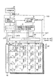
以下、本発明の一実施形態に係る液晶表示装置について添付図面を参照して説明する。図1はこの液晶表示装置の回路構成を概略的に示す。液晶表示装置は液晶表示パネルDPおよび表示パネル制御回路CNTを備える。液晶表示パネルDPは一対の電極基板であるアレイ基板1および対向基板2間に液晶層3を挟持した構造である。液晶層3は例えばノーマリホワイトの表示動作のために予めスプレー配向からベンド配向に転移されるOCB液晶である液晶材料を含む。表示パネル制御回路CNTはアレイ基板1および対向基板2から液晶層3に印加される液晶駆動電圧により液晶表示パネルDPの透過率を制御する。スプレー配向からベンド配向への転移は電源投入時に表示パネル制御回路CNTにより行われる所定の初期化処理で比較的大きな電界をOCB液晶に印加することにより得られる。液晶表示パネルDPはスプレー配向のエネルギーとベンド配向のエネルギーとが拮抗する転移境界値Vcを越える液晶駆動電圧Vpにおいて透過率の最小値および最大値を有し、表示パネル制御回路CNTは透過率の最小値および最大値に対応した範囲で液晶駆動電圧を変化させるように構成される。
Hereinafter, a liquid crystal display device according to an embodiment of the present invention will be described with reference to the accompanying drawings. FIG. 1 schematically shows a circuit configuration of the liquid crystal display device. The liquid crystal display device includes a liquid crystal display panel DP and a display panel control circuit CNT. The liquid crystal display panel DP has a structure in which a
アレイ基板1は、例えばガラス等の透明絶縁基板上に略マトリクス状に配置される複数の画素電極PE、複数の画素電極PEの行に沿って配置される複数のゲート線Y(Y0〜Ym)、複数の画素電極PEの列に沿って配置される複数のソース線X(X1〜Xn)、並びにこれらゲート線Yおよびソース線Xの交差位置近傍に配置され各々対応ゲート線Yを介して駆動されたときに対応ソース線Xおよび対応画素電極PE間で導通して複数の画素スイッチング素子Wを有する。各画素スイッチング素子Wは例えば薄膜トランジスタからなり、薄膜トランジスタのゲートがゲート線Yに接続され、ソース−ドレインパスがソース線Xおよび画素電極PE間に接続される。
The
対向基板2は例えばガラス等の透明絶縁基板上に配置されるカラーフィルタ、および複数の画素電極PEに対向してカラーフィルタ上に配置される共通電極CE等を含む。各画素電極PEおよび共通電極CEは例えばITO等の透明電極材料からなり、互いに平行にラビング処理される配向膜でそれぞれ覆われ、画素電極PEおよび共通電極CEからの電界に対応した液晶分子配列に制御される液晶層3の画素領域と共に画素PXを構成する。
The
また、複数の画素PXは各々画素電極PEおよび共通電極CE間に液晶容量CLCを有し、さらに複数の補助容量Csの一端に接続される。各補助容量Csは、この画素PXの画素電極PEとこの画素PXに一方側で隣接し画素PXの画素スイッチング素子Wを制御する前段のゲート線Yとの容量結合により形成され、この画素スイッチング素子Wの寄生容量に対して十分大きな容量値を有する。尚、図1は、表示画面を構成する複数の画素PXのマトリクスアレイに対して周囲に配置される複数のダミー画素を省略して描かれている。これらダミー画素は表示画面内の画素PXと同様に配線され、寄生容量等に関して表示画面内の全画素PXを同一条件にするために設けられものである。ゲート線Y0はこのようなダミー画素に対するゲート線である。 Each of the plurality of pixels PX has a liquid crystal capacitor CLC between the pixel electrode PE and the common electrode CE, and is further connected to one end of the plurality of auxiliary capacitors Cs. Each auxiliary capacitor Cs is formed by capacitive coupling between the pixel electrode PE of the pixel PX and the gate line Y adjacent to the pixel PX on one side and controlling the pixel switching element W of the pixel PX. It has a sufficiently large capacitance value with respect to the parasitic capacitance of W. In FIG. 1, a plurality of dummy pixels arranged around the matrix array of the plurality of pixels PX constituting the display screen are omitted. These dummy pixels are wired in the same manner as the pixels PX in the display screen, and are provided to make all the pixels PX in the display screen have the same conditions with respect to parasitic capacitance and the like. The gate line Y0 is a gate line for such a dummy pixel.
表示パネル制御回路CNTは、複数のスイッチング素子Wを行単位に導通させるように複数のゲート線Y0〜Ymを順次駆動するゲートドライバYD、各行のスイッチング素子Wが対応ゲート線Yの駆動によって導通する期間において画素電圧Vsを複数のソース線X1〜Xnにそれぞれ出力するソースドライバXD、複数の画素PXに対して1フレーム期間(垂直走査期間)毎に外部信号源SSから入力される複数の画素データからなる画像データに対して解像度および階調等の変換を行う画像データ変換回路4、およびこの画像データ変換回路4の変換結果として得られる画像データに対してゲートドライバYDおよびソースドライバXDの動作タイミング等を制御するコントローラ5を含む。画素電圧Vsは共通電極CEのコモン電圧Vcomを基準として画素電極PEに印加される電圧であり、例えばフレーム反転駆動およびライン反転駆動を行うようコモン電圧Vcomに対して極性反転される。
The display panel control circuit CNT includes a gate driver YD that sequentially drives the plurality of gate lines Y0 to Ym so that the plurality of switching elements W are conducted in units of rows, and the switching elements W in each row are conducted by driving the corresponding gate lines Y. A source driver XD that outputs the pixel voltage Vs to the plurality of source lines X1 to Xn in each period, and a plurality of pixel data input from the external signal source SS for each frame period (vertical scanning period) to the plurality of pixels PX. The image
ゲートドライバYDおよびソースドライバXDは例えばアレイ基板1の外縁に沿って配置されるフレキシブル配線シートにマウントされた集積回路(IC)チップである。他方、画像データ変換回路4およびコントローラ5は外部のプリント配線板PCB上に配置される。コントローラ5は、上述のように順次複数のゲート線Yを駆動するための制御信号CTYおよび、画像データ変換回路4の変換結果として1行分の画素PX単位に得られ直列に出力される画素データDATAを複数のソース線Xにそれぞれ割り当てると共に出力極性を指定する制御信号CTX等を発生する。制御信号CTYはコントローラ5からゲートドライバYDに供給され、制御信号CTXは画像データ変換回路4から変換結果として得られる画素データDATAと共にコントローラ5からソースドライバXDに供給される。
The gate driver YD and the source driver XD are, for example, integrated circuit (IC) chips mounted on a flexible wiring sheet disposed along the outer edge of the
表示パネル制御回路CNTはさらに1行分のスイッチング素子Wが非導通となるときにこれらスイッチング素子Wに接続されるゲート線Yに一方側で隣接する前段の隣接ゲート線YにゲートドライバYDを介して印加されこれらスイッチング素子Wの寄生容量によって1行分の画素PXに生じる画素電圧Vsの変動を補償する補償電圧Veを発生する補償電圧発生回路6、画像データDATAを画素電圧Vsに変換するために用いられる所定数の階調基準電圧VREFを発生する階調基準電圧発生回路7、および1水平走査期間(1H)毎にレベルシフトするコモン電圧Vcomを発生するコモン電圧発生回路8を含む。ここでは、コモン電圧発生回路8がコントローラ5からの制御信号CTXにより指定される出力極性を参照してコモン電圧Vcomを中心値Vcomc(=4V)に対してVcomc+2VおよびVcomc−2Vに交互に設定する。
The display panel control circuit CNT further passes through the gate driver YD to the adjacent adjacent gate line Y on one side adjacent to the gate line Y connected to the switching elements W when the switching elements W for one row become non-conductive. In order to convert the image data DATA into the pixel voltage Vs, the compensation
ゲートドライバYDは制御信号CTYの制御により1フレーム期間において複数のゲート線Y1〜Ymを順次選択し、各行の画素スイッチング素子Wを1水平走査期間だけ導通させるオン電圧を選択ゲート線Yに供給する。画像データ変換回路4は1行分の画素PXに対する画素データDATAからなる変換結果を1水平走査期間毎に出力し、ソースドライバXDは上述の階調基準電圧発生回路7から供給される所定数の階調基準電圧VREFを参照してこれら画素データDATAをそれぞれ画素電圧Vsに変換し、複数のソース線X1〜Xnに並列的に出力する。
The gate driver YD sequentially selects a plurality of gate lines Y1 to Ym in one frame period under the control of the control signal CTY, and supplies an ON voltage that makes the pixel switching elements W in each row conductive for one horizontal scanning period to the selected gate line Y. . The image
ゲートドライバYDが例えばゲート線Y1をオン電圧により駆動してこのゲート線Y1に接続された全ての画素スイッチング素子Wを導通させると、ソース線X1〜Xn上の画素電圧Vsがこれら画素スイッチング素子Wをそれぞれ介して対応画素電極PEおよび補助容量Csの一端に供給される。また、ゲートドライバYDはこのゲート線Y1に隣接した前段のゲート線Y0に補償電圧発生回路6からの補償電圧Veを出力し、ゲート線Y1に接続された全ての画素スイッチング素子Wを1水平走査期間だけ導通させた直後にこれら画素スイッチング素子Wを非導通にするオフ電圧をゲート線Y1に出力する。補償電圧Veはこれら画素スイッチング素子Wが非導通になったときにこれらの寄生容量によって画素電極PEから引き抜かれる電荷を低減して画素電圧Vsの変動、すなわち突き抜け電圧ΔVpを実質的にキャンセルする。
When the gate driver YD drives, for example, the gate line Y1 with the on-voltage to make all the pixel switching elements W connected to the gate line Y1 conductive, the pixel voltage Vs on the source lines X1 to Xn is changed to these pixel switching elements W. To the corresponding pixel electrode PE and one end of the auxiliary capacitor Cs. Further, the gate driver YD outputs the compensation voltage Ve from the compensation
図2は図1に示す液晶表示パネルDPにおいてシフトされる相対輝度(透過率)−液晶駆動電圧特性を示す。図2において、左側の特性グラフは典型的な液晶表示パネルの相対輝度(透過率)−液晶駆動電圧特性である。この場合、スプレー配向のエネルギーとベンド配向のエネルギーとが拮抗する転移境界値Vc(=1.6V)が透過率の最小値(=0%)および最大値(=100%)に対応する液晶駆動電圧Vpの0V〜4Vの範囲内に存在する。OCB液晶がベンド配向からスプレー配向への逆転移することを防止するために、液晶駆動電圧Vpを1.6V〜4Vの範囲で変化させることも考えられるが、これでは最大階調時の透過率が特性曲線に従って100%未満に制限され、ダイナミックレンジを低下させてしまう。これに対して、図1に示す液晶表示パネルDPでは、液晶層3のリタデーション値Δndが典型的なものよりも増大され、これにより相対輝度(透過率)−液晶駆動電圧特性が図2において右側の特性グラフに示すようにシフトされている。具体的には、液晶層3の厚さが4μm以上に設定され、OCB液晶の屈折率異方性Δnが0.165以上に設定される。ここでは、転移境界値Vc(=1.6V)は透過率の最小値(=0%)および最大値(=100%)に対応する液晶駆動電圧Vpの2V〜6Vの範囲より低い電圧レベルとして存在する。従って、液晶駆動電圧Vpを2V〜6Vの範囲で変化させたときに、Vc(=1.6V)<Vp(=2V〜6V)の関係になるため、OCB液晶は常にベンド配向に維持され、最大階調時の透過率も特性曲線に従って100%にできる。
FIG. 2 shows a relative luminance (transmittance) -liquid crystal driving voltage characteristic shifted in the liquid crystal display panel DP shown in FIG. In FIG. 2, the characteristic graph on the left is a relative luminance (transmittance) -liquid crystal driving voltage characteristic of a typical liquid crystal display panel. In this case, the transition boundary value Vc (= 1.6 V) at which the spray alignment energy and the bend alignment energy antagonize corresponds to the minimum value (= 0%) and maximum value (= 100%) of the transmittance. It exists in the range of 0V-4V of the voltage Vp. In order to prevent the OCB liquid crystal from making a reverse transition from bend alignment to spray alignment, it is conceivable to change the liquid crystal drive voltage Vp in the range of 1.6 V to 4 V, but this will cause the transmittance at the maximum gradation. Is limited to less than 100% in accordance with the characteristic curve, which reduces the dynamic range. On the other hand, in the liquid crystal display panel DP shown in FIG. 1, the retardation value Δnd of the
画素電圧Vsは図3に示すように行単位にコモン電圧Vcomに対して極性反転される。ここで、正極性の画素電圧を+Vs、負極性の画素電圧を−Vsで表すと、+Vs=4V〜8Vとなり、−Vs=4V〜0Vとなる。コモン電圧Vcomは、画素電圧Vsの振幅を不必要に増大させることなく100%の透過率を得られる2Vに液晶駆動電圧Vpの下限を設定するためにVcomc±2Vに設定される。画素電圧Vsおよびコモン電圧Vcomが図4に示すように1水平走査期間(1H)毎に同期して変化すると、液晶駆動電圧VpはVp=|+Vs−Vcom|またはVp=|−Vs−Vcom|となり、いずれの画素電圧極性でも2V〜6Vの範囲に設定される。 As shown in FIG. 3, the pixel voltage Vs is inverted in polarity with respect to the common voltage Vcom in units of rows. Here, when the positive pixel voltage is represented by + Vs and the negative pixel voltage is represented by −Vs, + Vs = 4V to 8V and −Vs = 4V to 0V. The common voltage Vcom is set to Vcomc ± 2V in order to set the lower limit of the liquid crystal driving voltage Vp to 2V that can obtain 100% transmittance without unnecessarily increasing the amplitude of the pixel voltage Vs. When the pixel voltage Vs and the common voltage Vcom change in synchronism with each horizontal scanning period (1H) as shown in FIG. 4, the liquid crystal driving voltage Vp becomes Vp = | + Vs−Vcom | or Vp = | −Vs−Vcom | Thus, any pixel voltage polarity is set in a range of 2V to 6V.
すなわち、表示パネル制御回路CNTは透過率の最小値および最大値に対応した振幅の画素電圧VsをソースドライバXDから複数の画素電極PEの各々にスイッチング素子Wを介して印加し、転移境界値Vcに対応したコモン電圧Vcomをコモン電圧発生回路8から共通電極CEに印加し、液晶駆動電圧Vpの極性を周期的に反転させるように画素電圧Vsおよびコモン電圧Vcomを設定する動作を行っている。
That is, the display panel control circuit CNT applies the pixel voltage Vs having an amplitude corresponding to the minimum value and the maximum value of the transmittance from the source driver XD to each of the plurality of pixel electrodes PE via the switching element W, and the transition boundary value Vc. Is applied to the common electrode CE from the common
本実施形態の液晶表示装置では、液晶表示パネルDPの透過率が転移境界値Vcを越える液晶駆動電圧Vpにおいて最小値および最大値となる。このような液晶表示パネルDPに対して、表示パネル制御回路CNTが透過率の最小値および最大値に対応した範囲で液晶駆動電圧Vpを変化させるように構成されるため、従来のような黒挿入駆動を必要としない。従って、液晶表示パネルDPの明るさを損なうことなくベンド配向からスプレー配向への逆転移を防止することができる。また、黒挿入駆動のための複雑な回路構造も必要とされない。 In the liquid crystal display device of this embodiment, the transmittance of the liquid crystal display panel DP becomes the minimum value and the maximum value at the liquid crystal drive voltage Vp that exceeds the transition boundary value Vc. For such a liquid crystal display panel DP, since the display panel control circuit CNT is configured to change the liquid crystal driving voltage Vp in a range corresponding to the minimum value and the maximum value of the transmittance, the conventional black insertion is performed. Does not require driving. Accordingly, reverse transition from bend alignment to spray alignment can be prevented without impairing the brightness of the liquid crystal display panel DP. Further, a complicated circuit structure for black insertion driving is not required.
次に、本発明の第2実施形態に係る液晶表示装置について説明する。 Next, a liquid crystal display device according to a second embodiment of the present invention will be described.
図5はこの液晶表示装置の回路構成を概略的に示す。この液晶表示装置は図2の右側に示すような相対輝度(透過率)−液晶駆動電圧特性を有する液晶表示パネルDPにおいてコモン電圧Vcomを一定にして2V〜6Vの範囲の液晶駆動電圧Vpを得るようにしたことが第1実施形態と相違する。このため、図5において、第1実施形態と同様部分を同一参照符号で表し、詳細な説明を簡単化あるいは省略する。 FIG. 5 schematically shows a circuit configuration of the liquid crystal display device. This liquid crystal display device obtains a liquid crystal drive voltage Vp in the range of 2V to 6V with a common voltage Vcom constant in a liquid crystal display panel DP having a relative luminance (transmittance) -liquid crystal drive voltage characteristic as shown on the right side of FIG. This is different from the first embodiment. Therefore, in FIG. 5, the same parts as those in the first embodiment are denoted by the same reference numerals, and detailed description thereof is simplified or omitted.
図5に示す液晶表示パネルDPでも、液晶層3の厚さが4μm以上に設定され、OCB液晶の屈折率異方性Δnが0.165以上に設定されている。また、コモン電圧発生回路8はコントローラ5から出力される制御信号CTXに関係なく6Vに固定されたコモン電圧Vcomを発生する。その代わり、ソースドライバXDから発生される画素電圧Vsの振幅が変更される。具体的には、正極性の画素電圧+Vsが+Vs=8V〜12Vに変更され、負極性の画素電圧−Vsが−Vs=4V〜0Vに変更される。
Also in the liquid crystal display panel DP shown in FIG. 5, the thickness of the
画素電圧Vsが図6に示すように1水平走査期間(1H)毎に変化すると、液晶駆動電圧VpはVp=|+Vs−Vcom|またはVp=|−Vs−Vcom|となり、いずれの画素電圧極性でも2V〜6Vの範囲に設定される。 When the pixel voltage Vs changes every horizontal scanning period (1H) as shown in FIG. 6, the liquid crystal driving voltage Vp becomes Vp = | + Vs−Vcom | or Vp = | −Vs−Vcom | However, it is set in the range of 2V to 6V.
すなわち、表示パネル制御回路CNTは透過率の最小値および最大値に対応した振幅に対して遷移境界値Vcに対応した振幅を加えた画素電圧VsをソースドライバXDから複数の画素電極PEの各々にスイッチング素子Wを介して印加し、一定のコモン電圧Vcomをコモン電圧発生回路8から共通電極CEに印加し、さらに液晶駆動電圧Vpの極性を周期的に反転させるように画素電圧Vsを設定する動作を行っている。
That is, the display panel control circuit CNT applies the pixel voltage Vs obtained by adding the amplitude corresponding to the transition boundary value Vc to the amplitude corresponding to the minimum value and the maximum value of the transmittance from the source driver XD to each of the plurality of pixel electrodes PE. An operation of applying the switching element W, applying a constant common voltage Vcom from the common
本実施形態の液晶表示装置では、第1実施形態よりも増大する出力振幅に適合するようにソースドライバXDの耐圧を上げる必要があるが、第1実施形態と同様の効果を得ることができる。すなわち、透過率が転移境界値Vcを越える液晶駆動電圧Vpにおいて最小値および最大値となる液晶表示パネルDPに対して、表示パネル制御回路CNTが透過率の最小値および最大値に対応した範囲で液晶駆動電圧Vpを変化させるように構成されるため、従来のような黒挿入駆動を必要としない。従って、液晶表示パネルDPの明るさを損なうことなくベンド配向からスプレー配向への逆転移を防止することができる。また、黒挿入駆動のための複雑な回路構造も必要とされない。 In the liquid crystal display device of the present embodiment, it is necessary to increase the withstand voltage of the source driver XD so as to match the output amplitude that is increased compared to the first embodiment, but the same effect as in the first embodiment can be obtained. That is, the display panel control circuit CNT has a range corresponding to the minimum value and the maximum value of the transmittance for the liquid crystal display panel DP having the minimum value and the maximum value at the liquid crystal driving voltage Vp where the transmittance exceeds the transition boundary value Vc. Since it is configured to change the liquid crystal drive voltage Vp, the conventional black insertion drive is not required. Accordingly, reverse transition from bend alignment to spray alignment can be prevented without impairing the brightness of the liquid crystal display panel DP. Further, a complicated circuit structure for black insertion driving is not required.
尚、本発明は上述の実施形態に限定されず、その要旨を逸脱しない範囲で様々に変形可能である。 In addition, this invention is not limited to the above-mentioned embodiment, It can deform | transform variously in the range which does not deviate from the summary.
例えば各々対応列の画素電極PEに容量結合させて複数のソース線Xに平行に複数の補助容量線を図1に示す液晶表示パネルDPに設け、表示パネル制御回路CNTからこれら補助容量線を選択的に介して画素電圧極性に対応したバイアス電圧を画素電極PEに印加することにより画素電圧Vsをバイアスして液晶駆動電圧Vpを2V〜6Vの範囲に設定してもよい。この場合、コモン電圧発生回路8は4Vに固定されたコモン電圧Vcomを発生するように構成すればよく、ソースドライバXDから出力される画素電圧Vsの振幅も変更する必要がない。
For example, a plurality of auxiliary capacitance lines are provided in the liquid crystal display panel DP shown in FIG. 1 in parallel with the plurality of source lines X by capacitive coupling to the pixel electrodes PE in the corresponding columns, and these auxiliary capacitance lines are selected from the display panel control circuit CNT. Therefore, the pixel voltage Vs may be biased by applying a bias voltage corresponding to the pixel voltage polarity to the pixel electrode PE to set the liquid crystal driving voltage Vp in the range of 2V to 6V. In this case, the common
1…アレイ基板、2…対向基板、3…液晶層、4…画像データ変換回路、5…コントローラ、6…補償電圧発生回路、7…階調基準電圧発生回路、8…コモン電圧発生回路、DP…液晶表示パネル、PE…画素電極、CE…共通電極、CLC…液晶容量、Cs…補助容量、PX…液晶画素、W…スイッチング素子、Y…ゲート線、X…ソース線、CNT…表示パネル制御回路、YD…ゲートドライバ、XD…ソースドライバ。
DESCRIPTION OF
Claims (5)
Priority Applications (2)
| Application Number | Priority Date | Filing Date | Title |
|---|---|---|---|
| JP2004308303A JP4528598B2 (en) | 2004-10-22 | 2004-10-22 | Liquid crystal display |
| US11/254,683 US20060092111A1 (en) | 2004-10-22 | 2005-10-21 | Liquid crystal display device |
Applications Claiming Priority (1)
| Application Number | Priority Date | Filing Date | Title |
|---|---|---|---|
| JP2004308303A JP4528598B2 (en) | 2004-10-22 | 2004-10-22 | Liquid crystal display |
Publications (3)
| Publication Number | Publication Date |
|---|---|
| JP2006119448A JP2006119448A (en) | 2006-05-11 |
| JP2006119448A5 JP2006119448A5 (en) | 2007-12-06 |
| JP4528598B2 true JP4528598B2 (en) | 2010-08-18 |
Family
ID=36261215
Family Applications (1)
| Application Number | Title | Priority Date | Filing Date |
|---|---|---|---|
| JP2004308303A Active JP4528598B2 (en) | 2004-10-22 | 2004-10-22 | Liquid crystal display |
Country Status (2)
| Country | Link |
|---|---|
| US (1) | US20060092111A1 (en) |
| JP (1) | JP4528598B2 (en) |
Families Citing this family (8)
| Publication number | Priority date | Publication date | Assignee | Title |
|---|---|---|---|---|
| JP4775057B2 (en) * | 2005-04-27 | 2011-09-21 | セイコーエプソン株式会社 | Liquid crystal device, driving method thereof, and electronic apparatus |
| KR100658276B1 (en) * | 2005-11-23 | 2006-12-14 | 삼성에스디아이 주식회사 | Liquid crystal display and driving method thereof |
| JP2008015179A (en) * | 2006-07-05 | 2008-01-24 | Toshiba Matsushita Display Technology Co Ltd | Liquid crystal display |
| JP5153438B2 (en) * | 2008-04-25 | 2013-02-27 | 統寶光電股▲ふん▼有限公司 | Liquid crystal display panel and display device |
| JP5025025B2 (en) | 2009-05-15 | 2012-09-12 | 株式会社ジャパンディスプレイセントラル | Liquid crystal display device and driving method of liquid crystal display device |
| JP5236815B2 (en) * | 2009-10-16 | 2013-07-17 | シャープ株式会社 | Display drive circuit, display device, and display drive method |
| JP4925371B2 (en) * | 2009-11-26 | 2012-04-25 | 東芝モバイルディスプレイ株式会社 | Liquid crystal display device and driving method of liquid crystal display device |
| CN103061650A (en) * | 2013-01-25 | 2013-04-24 | 彭艳兵 | Intelligent liquid crystal window controlling system and method thereof |
Citations (1)
| Publication number | Priority date | Publication date | Assignee | Title |
|---|---|---|---|---|
| JP2003035895A (en) * | 2000-10-25 | 2003-02-07 | Matsushita Electric Ind Co Ltd | Liquid crystal display device |
Family Cites Families (5)
| Publication number | Priority date | Publication date | Assignee | Title |
|---|---|---|---|---|
| JPS58191782A (en) * | 1982-04-30 | 1983-11-09 | Sharp Corp | Liquid crystal composition |
| JPH09218388A (en) * | 1996-02-09 | 1997-08-19 | Hosiden Corp | Liquid crystal display device |
| KR100666823B1 (en) * | 2000-07-06 | 2007-01-09 | 엘지.필립스 엘시디 주식회사 | Method for liquid crystal drving of tft lcd |
| TW546529B (en) * | 2001-06-20 | 2003-08-11 | Nec Lcd Technologies Ltd | OCB type liquid crystal display having transition nucleus area from splay alignment to bend alignment |
| KR100843685B1 (en) * | 2001-12-27 | 2008-07-04 | 엘지디스플레이 주식회사 | Method and apparatus for driving liquid crystal display |
-
2004
- 2004-10-22 JP JP2004308303A patent/JP4528598B2/en active Active
-
2005
- 2005-10-21 US US11/254,683 patent/US20060092111A1/en not_active Abandoned
Patent Citations (1)
| Publication number | Priority date | Publication date | Assignee | Title |
|---|---|---|---|---|
| JP2003035895A (en) * | 2000-10-25 | 2003-02-07 | Matsushita Electric Ind Co Ltd | Liquid crystal display device |
Also Published As
| Publication number | Publication date |
|---|---|
| JP2006119448A (en) | 2006-05-11 |
| US20060092111A1 (en) | 2006-05-04 |
Similar Documents
| Publication | Publication Date | Title |
|---|---|---|
| KR100732098B1 (en) | Light source device | |
| JP4551712B2 (en) | Gate line drive circuit | |
| KR100652096B1 (en) | Gate line driving circuit | |
| US20050200588A1 (en) | Liquid crystal display device | |
| KR101285054B1 (en) | Liquid crystal display device | |
| JP2007148369A (en) | Display control circuit, display control method, and display circuit | |
| JP2007241029A (en) | Liquid crystal display | |
| US20060092111A1 (en) | Liquid crystal display device | |
| JP2006058638A (en) | Gate line driving circuit | |
| JP4777050B2 (en) | Display panel control circuit | |
| JP2006349931A (en) | Liquid crystal display device | |
| US8085229B2 (en) | Optically compensated bend (OCB) liquid crystal display and method of operating same | |
| JP4275588B2 (en) | Liquid crystal display | |
| JP2007256488A (en) | Liquid crystal display device | |
| JP2007187995A (en) | Drive control circuit | |
| JP4851782B2 (en) | Liquid crystal display | |
| JP2006047848A (en) | Gate line driving circuit | |
| JP4874731B2 (en) | Liquid crystal display | |
| JP4862184B2 (en) | Liquid crystal display device and driving method thereof | |
| JP2007156013A (en) | Liquid crystal display panel | |
| JP2006349930A (en) | Liquid crystal display device | |
| JP4928789B2 (en) | Liquid crystal display | |
| US8436954B2 (en) | Method of driving liquid crystal display device, and liquid crystal display device | |
| JP2006078975A (en) | Display panel control circuit | |
| JP2006119449A (en) | Display panel control circuit |
Legal Events
| Date | Code | Title | Description |
|---|---|---|---|
| A521 | Request for written amendment filed |
Free format text: JAPANESE INTERMEDIATE CODE: A523 Effective date: 20071022 |
|
| A621 | Written request for application examination |
Free format text: JAPANESE INTERMEDIATE CODE: A621 Effective date: 20071022 |
|
| A977 | Report on retrieval |
Free format text: JAPANESE INTERMEDIATE CODE: A971007 Effective date: 20100318 |
|
| TRDD | Decision of grant or rejection written | ||
| A01 | Written decision to grant a patent or to grant a registration (utility model) |
Free format text: JAPANESE INTERMEDIATE CODE: A01 Effective date: 20100511 |
|
| A01 | Written decision to grant a patent or to grant a registration (utility model) |
Free format text: JAPANESE INTERMEDIATE CODE: A01 |
|
| A61 | First payment of annual fees (during grant procedure) |
Free format text: JAPANESE INTERMEDIATE CODE: A61 Effective date: 20100607 |
|
| FPAY | Renewal fee payment (event date is renewal date of database) |
Free format text: PAYMENT UNTIL: 20130611 Year of fee payment: 3 |
|
| R150 | Certificate of patent or registration of utility model |
Free format text: JAPANESE INTERMEDIATE CODE: R150 Ref document number: 4528598 Country of ref document: JP Free format text: JAPANESE INTERMEDIATE CODE: R150 |
|
| S533 | Written request for registration of change of name |
Free format text: JAPANESE INTERMEDIATE CODE: R313533 |
|
| FPAY | Renewal fee payment (event date is renewal date of database) |
Free format text: PAYMENT UNTIL: 20130611 Year of fee payment: 3 |
|
| R350 | Written notification of registration of transfer |
Free format text: JAPANESE INTERMEDIATE CODE: R350 |
|
| FPAY | Renewal fee payment (event date is renewal date of database) |
Free format text: PAYMENT UNTIL: 20140611 Year of fee payment: 4 |
|
| R250 | Receipt of annual fees |
Free format text: JAPANESE INTERMEDIATE CODE: R250 |
|
| R250 | Receipt of annual fees |
Free format text: JAPANESE INTERMEDIATE CODE: R250 |
|
| R250 | Receipt of annual fees |
Free format text: JAPANESE INTERMEDIATE CODE: R250 |
|
| R250 | Receipt of annual fees |
Free format text: JAPANESE INTERMEDIATE CODE: R250 |
|
| R250 | Receipt of annual fees |
Free format text: JAPANESE INTERMEDIATE CODE: R250 |
|
| R250 | Receipt of annual fees |
Free format text: JAPANESE INTERMEDIATE CODE: R250 |
|
| R250 | Receipt of annual fees |
Free format text: JAPANESE INTERMEDIATE CODE: R250 |
|
| S111 | Request for change of ownership or part of ownership |
Free format text: JAPANESE INTERMEDIATE CODE: R313111 |
|
| R250 | Receipt of annual fees |
Free format text: JAPANESE INTERMEDIATE CODE: R250 |
|
| R350 | Written notification of registration of transfer |
Free format text: JAPANESE INTERMEDIATE CODE: R350 |
|
| R250 | Receipt of annual fees |
Free format text: JAPANESE INTERMEDIATE CODE: R250 |
|
| R250 | Receipt of annual fees |
Free format text: JAPANESE INTERMEDIATE CODE: R250 |
|
| R250 | Receipt of annual fees |
Free format text: JAPANESE INTERMEDIATE CODE: R250 |