EP2490159B1 - Entité électronique avec moyens de communication par contact et à distance - Google Patents
Entité électronique avec moyens de communication par contact et à distance Download PDFInfo
- Publication number
- EP2490159B1 EP2490159B1 EP12159987.2A EP12159987A EP2490159B1 EP 2490159 B1 EP2490159 B1 EP 2490159B1 EP 12159987 A EP12159987 A EP 12159987A EP 2490159 B1 EP2490159 B1 EP 2490159B1
- Authority
- EP
- European Patent Office
- Prior art keywords
- electronic entity
- activation
- information item
- communication means
- data
- Prior art date
- Legal status (The legal status is an assumption and is not a legal conclusion. Google has not performed a legal analysis and makes no representation as to the accuracy of the status listed.)
- Active
Links
Images

Classifications
-
- G—PHYSICS
- G06—COMPUTING OR CALCULATING; COUNTING
- G06K—GRAPHICAL DATA READING; PRESENTATION OF DATA; RECORD CARRIERS; HANDLING RECORD CARRIERS
- G06K19/00—Record carriers for use with machines and with at least a part designed to carry digital markings
- G06K19/06—Record carriers for use with machines and with at least a part designed to carry digital markings characterised by the kind of the digital marking, e.g. shape, nature, code
- G06K19/067—Record carriers with conductive marks, printed circuits or semiconductor circuit elements, e.g. credit or identity cards also with resonating or responding marks without active components
- G06K19/07—Record carriers with conductive marks, printed circuits or semiconductor circuit elements, e.g. credit or identity cards also with resonating or responding marks without active components with integrated circuit chips
- G06K19/073—Special arrangements for circuits, e.g. for protecting identification code in memory
-
- G—PHYSICS
- G06—COMPUTING OR CALCULATING; COUNTING
- G06K—GRAPHICAL DATA READING; PRESENTATION OF DATA; RECORD CARRIERS; HANDLING RECORD CARRIERS
- G06K7/00—Methods or arrangements for sensing record carriers, e.g. for reading patterns
- G06K7/10—Methods or arrangements for sensing record carriers, e.g. for reading patterns by electromagnetic radiation, e.g. optical sensing; by corpuscular radiation
- G06K7/10009—Methods or arrangements for sensing record carriers, e.g. for reading patterns by electromagnetic radiation, e.g. optical sensing; by corpuscular radiation sensing by radiation using wavelengths larger than 0.1 mm, e.g. radio-waves or microwaves
- G06K7/10198—Methods or arrangements for sensing record carriers, e.g. for reading patterns by electromagnetic radiation, e.g. optical sensing; by corpuscular radiation sensing by radiation using wavelengths larger than 0.1 mm, e.g. radio-waves or microwaves setting parameters for the interrogator, e.g. programming parameters and operating modes
-
- B—PERFORMING OPERATIONS; TRANSPORTING
- B42—BOOKBINDING; ALBUMS; FILES; SPECIAL PRINTED MATTER
- B42D—BOOKS; BOOK COVERS; LOOSE LEAVES; PRINTED MATTER CHARACTERISED BY IDENTIFICATION OR SECURITY FEATURES; PRINTED MATTER OF SPECIAL FORMAT OR STYLE NOT OTHERWISE PROVIDED FOR; DEVICES FOR USE THEREWITH AND NOT OTHERWISE PROVIDED FOR; MOVABLE-STRIP WRITING OR READING APPARATUS
- B42D25/00—Information-bearing cards or sheet-like structures characterised by identification or security features; Manufacture thereof
- B42D25/20—Information-bearing cards or sheet-like structures characterised by identification or security features; Manufacture thereof characterised by a particular use or purpose
- B42D25/22—Information-bearing cards or sheet-like structures characterised by identification or security features; Manufacture thereof characterised by a particular use or purpose for use in combination with accessories specially adapted for information-bearing cards
-
- G—PHYSICS
- G06—COMPUTING OR CALCULATING; COUNTING
- G06K—GRAPHICAL DATA READING; PRESENTATION OF DATA; RECORD CARRIERS; HANDLING RECORD CARRIERS
- G06K19/00—Record carriers for use with machines and with at least a part designed to carry digital markings
- G06K19/06—Record carriers for use with machines and with at least a part designed to carry digital markings characterised by the kind of the digital marking, e.g. shape, nature, code
- G06K19/067—Record carriers with conductive marks, printed circuits or semiconductor circuit elements, e.g. credit or identity cards also with resonating or responding marks without active components
- G06K19/07—Record carriers with conductive marks, printed circuits or semiconductor circuit elements, e.g. credit or identity cards also with resonating or responding marks without active components with integrated circuit chips
- G06K19/0723—Record carriers with conductive marks, printed circuits or semiconductor circuit elements, e.g. credit or identity cards also with resonating or responding marks without active components with integrated circuit chips the record carrier comprising an arrangement for non-contact communication, e.g. wireless communication circuits on transponder cards, non-contact smart cards or RFIDs
-
- G—PHYSICS
- G06—COMPUTING OR CALCULATING; COUNTING
- G06K—GRAPHICAL DATA READING; PRESENTATION OF DATA; RECORD CARRIERS; HANDLING RECORD CARRIERS
- G06K19/00—Record carriers for use with machines and with at least a part designed to carry digital markings
- G06K19/06—Record carriers for use with machines and with at least a part designed to carry digital markings characterised by the kind of the digital marking, e.g. shape, nature, code
- G06K19/067—Record carriers with conductive marks, printed circuits or semiconductor circuit elements, e.g. credit or identity cards also with resonating or responding marks without active components
- G06K19/07—Record carriers with conductive marks, printed circuits or semiconductor circuit elements, e.g. credit or identity cards also with resonating or responding marks without active components with integrated circuit chips
- G06K19/077—Constructional details, e.g. mounting of circuits in the carrier
- G06K19/07716—Constructional details, e.g. mounting of circuits in the carrier the record carrier comprising means for customization, e.g. being arranged for personalization in batch
-
- G—PHYSICS
- G06—COMPUTING OR CALCULATING; COUNTING
- G06K—GRAPHICAL DATA READING; PRESENTATION OF DATA; RECORD CARRIERS; HANDLING RECORD CARRIERS
- G06K19/00—Record carriers for use with machines and with at least a part designed to carry digital markings
- G06K19/06—Record carriers for use with machines and with at least a part designed to carry digital markings characterised by the kind of the digital marking, e.g. shape, nature, code
- G06K19/067—Record carriers with conductive marks, printed circuits or semiconductor circuit elements, e.g. credit or identity cards also with resonating or responding marks without active components
- G06K19/07—Record carriers with conductive marks, printed circuits or semiconductor circuit elements, e.g. credit or identity cards also with resonating or responding marks without active components with integrated circuit chips
- G06K19/077—Constructional details, e.g. mounting of circuits in the carrier
- G06K19/07749—Constructional details, e.g. mounting of circuits in the carrier the record carrier being capable of non-contact communication, e.g. constructional details of the antenna of a non-contact smart card
- G06K19/07766—Constructional details, e.g. mounting of circuits in the carrier the record carrier being capable of non-contact communication, e.g. constructional details of the antenna of a non-contact smart card comprising at least a second communication arrangement in addition to a first non-contact communication arrangement
- G06K19/07769—Constructional details, e.g. mounting of circuits in the carrier the record carrier being capable of non-contact communication, e.g. constructional details of the antenna of a non-contact smart card comprising at least a second communication arrangement in addition to a first non-contact communication arrangement the further communication means being a galvanic interface, e.g. hybrid or mixed smart cards having a contact and a non-contact interface
-
- H—ELECTRICITY
- H04—ELECTRIC COMMUNICATION TECHNIQUE
- H04L—TRANSMISSION OF DIGITAL INFORMATION, e.g. TELEGRAPHIC COMMUNICATION
- H04L9/00—Cryptographic mechanisms or cryptographic arrangements for secret or secure communications; Network security protocols
- H04L9/32—Cryptographic mechanisms or cryptographic arrangements for secret or secure communications; Network security protocols including means for verifying the identity or authority of a user of the system or for message authentication, e.g. authorization, entity authentication, data integrity or data verification, non-repudiation, key authentication or verification of credentials
Definitions
- the invention relates to an electronic entity with contact communication means and remote communication means, more specifically a method of personalizing this electronic entity.
- An electronic entity such as for example a microcircuit card, which generally includes electronic circuits capable of storing information, has means of communication with the outside, in particular for exchanging information held by the electronic entity with external devices, of the reader or terminal type.
- contact communication means are distinguished, for which a physical contact between the electronic entity and the terminal is a necessary condition for the establishment of a communication, and the means of remote communication. , thanks to which communication between the electronic entity and a reader is possible without physical contact between these two elements, with a range of the order of a few centimeters in general.
- Some electronic entities also include communication means of the two aforementioned types, in which case the " contact " and “ contactless " operating modes can be organized according to the required functionalities of the apparatus for each of the communication modes, such as this is for example described in patents US 5,206,495 and US 5,999,713 .
- contactless communication means Although the use of contactless communication means is known for its practicality (because no precise positioning of the electronic entity is necessary for the exchange of information), it nevertheless has the disadvantage of risk of unwanted exchange of information, for example by establishing an unwanted communication by the user when passing near a reader. This problem is particularly sensitive when the electronic entity holds confidential information, for example in the case of an electronic passport.
- the patent application DE 199 08 285 describes the loading of personalization data in a microcircuit card through contacts of the card.
- the patent application WO 98/37526 describes a multi-application card in which personalization data stored on the card is consulted to determine whether an application can be loaded therein.
- the possibility of exchanging the data by the remote communication means can thus be managed via the contact link, for example by means of a terminal.
- the exchange of data concerned by the authorization is for example the emission of at least some data and / or the reception of certain data at least.
- the electronic entity also comprises means for memorizing an activation information commanded by said instruction and means for authorizing the exchange (transmission and / or reception) of said data through the remote communication means in the presence of said activation information.
- the electronic entity may also further comprise means for inhibiting the exchange of said data through the remote communication means in the absence of said activation information.
- the electronic entity is for example a microcircuit card compliant with ISO14443 and / or ISO7816.
- the determined time may correspond to the receipt of an end of communication command by the remote communication means, which allows the instruction to allow only one communication.
- the determined time can be determined by a delay, which limits the duration of the authorization in time.
- the determined time can be reached after receiving a predetermined number of commands via the remote communication means, which limits the possibilities of use of the authorization.
- the determined time may correspond to the completion of a step of initializing the communication.
- This method may further comprise a step of writing a configuration information representative of the conditions for modifying the activation information. It is thus possible to configure the electronic entity with regard to the possibilities of using the remote communication means during personalization as a function of its subsequent use, without this implying any modifications of the circuits used.
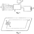
- the figure 1 represents the main elements of an electronic entity: this electronic entity comprises a microcircuit 12 (for example a microprocessor) which can be connected to an external device of the terminal type by means of contacts 14 in order to establish a communication of the " by contact " type "between the electronic entity and this terminal.
- a microcircuit 12 for example a microprocessor
- the electronic entity also comprises an antenna 16 connected at each of its ends to a corresponding terminal of the microcircuit 12.
- the antenna 16 is part of the remote communication means of the electronic entity.
- a rewritable memory 18 (for example a non-volatile memory of the erasable and electronically programmable memory type, generally designated by the acronym EEPROM) is also connected to the microcircuit 12.
- EEPROM electronically programmable memory
- the microcircuit 12 can be fed through the contact link (via at least one of the contacts 14) or, independently of this first power supply, by a remote power supply the magnetic antenna 16.
- the use of the " contactless " communication mode will therefore not be conditioned by the simultaneous use of the contact link (through the contacts 14).
- the electronic entity can therefore be powered either by the contact connection or by remote power supply, which gives rise to two main modes of operation described respectively in FIG. Figures 3 and 4 ; simultaneous power supply by contact power and remote power supply is naturally possible without calling into question the operating principles of the two modes described above.
- FIG. figure 3 When communicating the electronic entity with a terminal through the contacts 14, the method illustrated in FIG. figure 3 is implemented under the control of the microcircuit 12 (for example programmed by means of instructions stored in memory).
- an activation bit is set to 0. stored for example in the rewritable memory 18, which indicates that, by default, a remote communication is inhibited (as will be described in detail below).
- the microcircuit can receive from the terminal an activation instruction of the contactless communication, that is to say a data (or more generally information) which aims to control the authorization of a " contactless " operation through the antenna 16, as explained with reference to the figure 4 (step E20).
- an activation instruction of the contactless communication that is to say a data (or more generally information) which aims to control the authorization of a " contactless " operation through the antenna 16, as explained with reference to the figure 4 (step E20).
- a code provided by the user (for example by means of a keyboard) to the terminal is transmitted in association with the activation instruction so that the authorization of operation in " contactless "is effective only in the presence of the correct code provided by the user, that is to say a predetermined code and stored (possibly in protected form) in the rewritable memory 18 associated with the microcircuit 12 (or in another memory, of the type ROM, associated with this microcircuit 12).
- the microcircuit 12 After receiving the activation instruction accompanied by the code provided by the user, the microcircuit 12 proceeds to a verification step E22 the accuracy of the code provided, that is to say in practice of comparison of the code provided to the code stored in the electronic entity as already mentioned.
- the authorization of a contactless communication becomes effective by setting the activation bit mentioned in step E24 to 1, which means that the electronic entity has actually received activation information of the correct contactless communication.
- step E20 if the code provided by the user is transmitted to the electronic entity with the activation instruction in step E20 is not the code stored by it, proceed to step E26 to setting the activation bit to 0 in rewritable memory 18, which means that it is considered then that no valid activation information has been received.
- the activation bit is modified for example by an instruction of the " UPDATE BINARY” type (defined by the ISO7816-4 standard) after selecting the file containing this activation bit by a command of the " SELECT " type. ".
- step E26 is not necessary since it does not change a priori the value of the activation bit. However, one may wish to use it, for example to make sure that any use of an incorrect code leads to setting the activation bit to 0 even if the correct code has been subjected to a previous phase. Moreover, in the presence or absence of step E26, the reception of an incorrect code could lead to other consequences, such as for example the transmission of an error message from the card to the terminal via the contacts 14.
- step E30 Upon entry of the electronic entity in the reader's field (step E30), the electronic entity is remote powered (which can be seen as a detection of the reader by the electronic entity) and the microcircuit 12 begins its operation in " contactless " mode.
- the microcircuit 12 proceeds to read in the rewritable memory 18 of the activation bit (step E32).
- step E34 it can then proceed to step E34 to check the value of the activation bit (which, as already indicated, is indicative of activation information of the contactless communication).
- step E36 is terminated at contactless communication, of which only the first steps will have been realized without this implying an exchange of data.
- the microcircuit 12 determines whether the activation bit stored in the rewritable memory 18 is at the value 1 (that is to say, it is in the presence of information of activation)
- it proceeds to the continuation of the implementation of the contactless communication, namely first of all an initialization of the contactless connection protocol in step E38 (for example according to ISO14443-4 in order to arrive at the execution level of the " Half-Duplex Block Transmission Protocol ”) .
- step E40 the activation bit in rewritable memory 18 is set to 0, as represented by step E40 on FIG. figure 4 .
- the implementation of step E40 after the initialization of the protocol makes it possible to ensure that the electronic entity will not be authorized to establish a new contactless communication after having left the reader's field (except to receive a new instruction activation by means of the contact link).
- the setting of 0 of the activation bit could occur under other conditions, such as for example a delay with respect to the moment of reception of the activation instruction (or possibly with respect to the establishment of the contactless link), the execution of a predetermined number of instructions by the microcircuit 12 (or APDU " Application Protocol Data Unit " commands) or the receipt of an end-of-transaction message (as was the case in the first embodiment).
- the activation bit is not reset to 0 during operation in contactless mode, but rather to reception of a deactivation instruction in " contact " mode.
- a deactivation instruction could also be provided even for the case where the activation bit is reset to zero during non-contact operation (as for example described in FIG. figure 4 ).
- step E42 a data exchange is carried out according to the contactless protocol at a step E42.
- the data exchange of the step E42 is completed, for example by the output of the electronic entity of the reader's field, or alternatively on receiving it from a command terminating the contactless communication, the activation bit having been reset to 0 by the step E40, a new iteration of the steps E30 to E34 by the return of the electronic entity in the reader's field will lead to a failure of the communication without contact by going to step E36.
- the activation bit (used as an indicator of the prior receipt of a valid activation instruction) conditions all the data exchanges in contactless mode.
- this activation bit conditions only the exchange of certain particular data of the electronic entity, whereas other data could be freely communicated by the electronic entity when it passes close to a remote reader, even if no specific instructions have been received by the prior contact link.
- the electronic entity when the electronic entity is an electronic identification document, provision can be made for certain data present on the document (such as the name of the person concerned) to be communicated without first requiring the activation of a particular authorization, whereas that the transmission of other data (for example, confidential information of the biometric data type - fingerprint, iris or facial image) can only be issued by the electronic entity via the contactless link provided that the entity electronics has previously received a valid activation instruction in this direction by means of the contact link.
- certain data present on the document such as the name of the person concerned
- other data for example, confidential information of the biometric data type - fingerprint, iris or facial image
- the presence of activation information ie the value 1 of the activation bit
- the presence of activation information will not condition the establishment of the contactless link itself, but some steps of issue of confidential data.
- the activation instruction does not correspond to the authorization to transmit that data only once, that is to say that the activation bit would then be reset to 0 immediately. after the transmission of confidential data.
- the activation information can be used to condition the reception of data via the contactless link. It is thus possible to avoid for example an identification code being presented to the electronic entity via the contactless link by a malicious third party, without the knowledge of the authorized carrier of the electronic entity, at the risk for example of blocking the electronic identity. electronic entity following the presentation of several fake codes by this third party.
- the data concerned by the exchange authorization are not necessarily limited to the application data of the electronic entity (that is to say in particular the data carried by the electronic entity in its support function of information), but may also include data of other types, such as data for establishing a communication protocol.
Landscapes
- Engineering & Computer Science (AREA)
- Physics & Mathematics (AREA)
- General Physics & Mathematics (AREA)
- Theoretical Computer Science (AREA)
- Computer Hardware Design (AREA)
- Microelectronics & Electronic Packaging (AREA)
- Computer Networks & Wireless Communication (AREA)
- Computer Security & Cryptography (AREA)
- Health & Medical Sciences (AREA)
- Toxicology (AREA)
- Artificial Intelligence (AREA)
- Computer Vision & Pattern Recognition (AREA)
- General Health & Medical Sciences (AREA)
- Electromagnetism (AREA)
- General Engineering & Computer Science (AREA)
- Signal Processing (AREA)
- Mobile Radio Communication Systems (AREA)
- Storage Device Security (AREA)
- Lock And Its Accessories (AREA)
- Catching Or Destruction (AREA)
- Telephone Function (AREA)
Priority Applications (1)
| Application Number | Priority Date | Filing Date | Title |
|---|---|---|---|
| PL12159987T PL2490159T3 (pl) | 2005-07-25 | 2006-07-24 | Jednostka elektroniczna ze środkami łączności stykowej i zdalnej |
Applications Claiming Priority (2)
| Application Number | Priority Date | Filing Date | Title |
|---|---|---|---|
| FR0507887A FR2888976B1 (fr) | 2005-07-25 | 2005-07-25 | Entite electronique avec moyens de communication par contact et a distance |
| EP06778905.7A EP1907993B2 (fr) | 2005-07-25 | 2006-07-24 | Entite electronique avec moyens de communication par contact et a distance |
Related Parent Applications (2)
| Application Number | Title | Priority Date | Filing Date |
|---|---|---|---|
| EP06778905.7A Division EP1907993B2 (fr) | 2005-07-25 | 2006-07-24 | Entite electronique avec moyens de communication par contact et a distance |
| EP06778905.7A Division-Into EP1907993B2 (fr) | 2005-07-25 | 2006-07-24 | Entite electronique avec moyens de communication par contact et a distance |
Publications (2)
| Publication Number | Publication Date |
|---|---|
| EP2490159A1 EP2490159A1 (fr) | 2012-08-22 |
| EP2490159B1 true EP2490159B1 (fr) | 2017-12-27 |
Family
ID=36202430
Family Applications (2)
| Application Number | Title | Priority Date | Filing Date |
|---|---|---|---|
| EP12159987.2A Active EP2490159B1 (fr) | 2005-07-25 | 2006-07-24 | Entité électronique avec moyens de communication par contact et à distance |
| EP06778905.7A Active EP1907993B2 (fr) | 2005-07-25 | 2006-07-24 | Entite electronique avec moyens de communication par contact et a distance |
Family Applications After (1)
| Application Number | Title | Priority Date | Filing Date |
|---|---|---|---|
| EP06778905.7A Active EP1907993B2 (fr) | 2005-07-25 | 2006-07-24 | Entite electronique avec moyens de communication par contact et a distance |
Country Status (13)
| Country | Link |
|---|---|
| US (2) | US9111188B2 (enExample) |
| EP (2) | EP2490159B1 (enExample) |
| JP (4) | JP2009503665A (enExample) |
| KR (1) | KR101156298B1 (enExample) |
| CY (1) | CY1114976T1 (enExample) |
| DK (1) | DK1907993T4 (enExample) |
| ES (2) | ES2450193T5 (enExample) |
| FR (1) | FR2888976B1 (enExample) |
| HU (1) | HUE036644T2 (enExample) |
| PL (2) | PL1907993T5 (enExample) |
| PT (2) | PT2490159T (enExample) |
| SI (1) | SI1907993T2 (enExample) |
| WO (1) | WO2007012738A1 (enExample) |
Families Citing this family (13)
| Publication number | Priority date | Publication date | Assignee | Title |
|---|---|---|---|---|
| FR2888976B1 (fr) * | 2005-07-25 | 2007-10-12 | Oberthur Card Syst Sa | Entite electronique avec moyens de communication par contact et a distance |
| JP4457241B2 (ja) * | 2007-06-28 | 2010-04-28 | フェリカネットワークス株式会社 | 情報処理システム、リーダ/ライタ、情報処理装置、アクセス制限管理方法、およびプログラム |
| CN101970638B (zh) | 2007-10-03 | 2015-02-11 | 纳幕尔杜邦公司 | 用于高水平生产二十碳五烯酸的优化解脂耶氏酵母菌株 |
| JP4640451B2 (ja) | 2008-06-06 | 2011-03-02 | ソニー株式会社 | 接触・非接触複合icカード、通信方法、プログラム及び通信システム |
| WO2010037361A1 (de) * | 2008-09-30 | 2010-04-08 | Deutsche Telekom Ag | Verfahren und kommunikationssystem zum berechtigungsabhängigen steuern einer kontaktlosen schnittstelleneinrichtung |
| FR2938090B1 (fr) | 2008-10-30 | 2010-12-31 | Oberthur Technologies | Carte d'identification d'abonne a un reseau de telephonie et procede de commande d'un dispositif electronique apte a interagir avec une telle carte |
| FR2938097B1 (fr) * | 2008-10-30 | 2010-12-31 | Oberthur Technologies | Carte a microcircuit, dispositif electronique associe a une telle carte, et procede de commande d'un tel dispositif electronique |
| FR2942060B1 (fr) | 2009-02-11 | 2016-02-12 | Oberthur Technologies | Entite electronique apte a communiquer avec un lecteur et procede mis en oeuvre au sein d'une telle entite electronique |
| US8320962B2 (en) * | 2009-06-05 | 2012-11-27 | Visa International Service Association | Contactless disablement |
| US8430323B2 (en) | 2009-06-12 | 2013-04-30 | Oberthur Technologies of America Corp. | Electronic device and associated method |
| US8838709B2 (en) * | 2010-12-17 | 2014-09-16 | Silverpop Systems, Inc. | Anti-phishing electronic message verification |
| US9141904B2 (en) * | 2011-03-31 | 2015-09-22 | Panasonic Intellectual Property Corporation Of America | RFID device, host, RFID-embedded apparatus, and method of controlling RFID device |
| FR3061332B1 (fr) * | 2016-12-23 | 2019-05-31 | Idemia France | Procede pour la securite d'une operation electronique avec une carte a puce |
Citations (1)
| Publication number | Priority date | Publication date | Assignee | Title |
|---|---|---|---|---|
| WO1999034326A1 (en) * | 1997-12-31 | 1999-07-08 | On Track Innovations Ltd. | Contact/contactless smart card having customizable antenna interface |
Family Cites Families (37)
| Publication number | Priority date | Publication date | Assignee | Title |
|---|---|---|---|---|
| KR850000074A (ko) * | 1983-05-13 | 1985-02-25 | 진 자콘 | 신호제어 파형 기록기 |
| JPH0734217B2 (ja) * | 1985-10-29 | 1995-04-12 | オムロン株式会社 | カードシステム |
| US4764666A (en) * | 1987-09-18 | 1988-08-16 | Gtech Corporation | On-line wagering system with programmable game entry cards |
| DE3935364C1 (enExample) * | 1989-10-24 | 1990-08-23 | Angewandte Digital Elektronik Gmbh, 2051 Brunstorf, De | |
| DE19531372A1 (de) | 1995-08-25 | 1997-02-27 | Siemens Ag | Chipkarte |
| JP3360002B2 (ja) * | 1996-03-14 | 2002-12-24 | 沖電気工業株式会社 | 接触式・非接触式兼用icカード及び接触式・非接触式兼用icカードリーダライタ |
| JPH10207997A (ja) * | 1997-01-20 | 1998-08-07 | Central Japan Railway Co | Icカードホルダ |
| GB2321744B (en) * | 1997-01-30 | 2000-05-17 | Motorola Inc | Portable data carrier and method for selecting operating mode thereof |
| US6575372B1 (en) * | 1997-02-21 | 2003-06-10 | Mondex International Limited | Secure multi-application IC card system having selective loading and deleting capability |
| US6025780A (en) | 1997-07-25 | 2000-02-15 | Checkpoint Systems, Inc. | RFID tags which are virtually activated and/or deactivated and apparatus and methods of using same in an electronic security system |
| DE19742126A1 (de) | 1997-09-24 | 1999-03-25 | Siemens Ag | Tragbarer Datenträger mit Aktivierungsschalter |
| ATE430340T1 (de) * | 1998-03-24 | 2009-05-15 | Toshiba Kk | Tragbare elektronische vorrichtung mit kontaktbehafteten und kontaktlosen schnittstellen |
| JP2000163546A (ja) * | 1998-11-25 | 2000-06-16 | Tokin Corp | Icカード及びその使用方法 |
| DE19908285A1 (de) * | 1999-02-26 | 2000-08-31 | Orga Kartensysteme Gmbh | Vorrichtung zum Laden einer Chipkarte mit Personalisierungsdaten |
| DE19950524A1 (de) * | 1999-10-20 | 2001-04-26 | Philips Corp Intellectual Pty | Chipkarte |
| JP2001323695A (ja) * | 2000-05-17 | 2001-11-22 | Dainippon Printing Co Ltd | 入退室管理システム |
| FR2809516A1 (fr) * | 2000-05-25 | 2001-11-30 | Innovatron Electronique | Systeme pour proteger contre la fraude des objets portatifs tels que des cartes a microcircuits mixtes a contacts/sans contact |
| DE10028821A1 (de) * | 2000-06-10 | 2001-12-20 | Miditec Datensysteme Gmbh | Chipkarte mit Lesekennungen |
| JP2002183704A (ja) * | 2000-12-11 | 2002-06-28 | Toshiba Corp | 無線通信カード及び情報処理装置 |
| JP2002197432A (ja) * | 2000-12-27 | 2002-07-12 | Canon Inc | メモリカード |
| EP1258831B1 (en) * | 2001-05-17 | 2006-07-26 | Matsushita Electric Industrial Co., Ltd. | IC Card and Electronic Devices having contact and non-contact interface |
| JP2003132313A (ja) * | 2001-10-24 | 2003-05-09 | Toshiba Corp | コンビカード用lsi、コンビカード及びコンビカードの使用方法 |
| US7344074B2 (en) * | 2002-04-08 | 2008-03-18 | Nokia Corporation | Mobile terminal featuring smart card interrupt |
| US6776339B2 (en) * | 2002-09-27 | 2004-08-17 | Nokia Corporation | Wireless communication device providing a contactless interface for a smart card reader |
| JP2005222097A (ja) * | 2004-02-03 | 2005-08-18 | Dainippon Printing Co Ltd | 携帯機器 |
| JP2004349994A (ja) * | 2003-05-22 | 2004-12-09 | Hitachi Ltd | 通信システム、携帯端末、icカード、および通信方法 |
| US7472834B2 (en) * | 2003-07-09 | 2009-01-06 | Stmicroelectronics S.A. | Dual-mode smart card |
| US7237719B2 (en) * | 2003-09-03 | 2007-07-03 | Stmicroelectronics, Inc. | Method and apparatus for a USB and contactless smart card device |
| GB0322694D0 (en) * | 2003-09-27 | 2003-10-29 | Hewlett Packard Development Co | A memory tag and a reader |
| JP4417705B2 (ja) * | 2003-12-10 | 2010-02-17 | 大日本印刷株式会社 | 携帯型情報記憶媒体、そのホルダ及び携帯型情報記憶媒体のプログラム |
| US20060113381A1 (en) * | 2004-11-29 | 2006-06-01 | John Hochstein | Batteryless contact fingerprint-enabled smartcard that enables contactless capability |
| JP5507811B2 (ja) * | 2005-02-15 | 2014-05-28 | ヴォウダフォン・グループ・ピーエルシー | 無線通信のための向上したセキュリティ |
| WO2006138440A2 (en) † | 2005-06-16 | 2006-12-28 | Visa International Service Association | Contactless activation systems and methods |
| FR2888976B1 (fr) * | 2005-07-25 | 2007-10-12 | Oberthur Card Syst Sa | Entite electronique avec moyens de communication par contact et a distance |
| JP2007257542A (ja) * | 2006-03-24 | 2007-10-04 | Toshiba Corp | 複合携帯可能電子装置および複合icカード |
| US8320962B2 (en) * | 2009-06-05 | 2012-11-27 | Visa International Service Association | Contactless disablement |
| US9141904B2 (en) * | 2011-03-31 | 2015-09-22 | Panasonic Intellectual Property Corporation Of America | RFID device, host, RFID-embedded apparatus, and method of controlling RFID device |
-
2005
- 2005-07-25 FR FR0507887A patent/FR2888976B1/fr not_active Expired - Lifetime
-
2006
- 2006-07-24 JP JP2008523404A patent/JP2009503665A/ja not_active Withdrawn
- 2006-07-24 US US11/919,551 patent/US9111188B2/en active Active
- 2006-07-24 DK DK06778905.7T patent/DK1907993T4/da active
- 2006-07-24 PT PT121599872T patent/PT2490159T/pt unknown
- 2006-07-24 ES ES06778905T patent/ES2450193T5/es active Active
- 2006-07-24 EP EP12159987.2A patent/EP2490159B1/fr active Active
- 2006-07-24 PL PL06778905.7T patent/PL1907993T5/pl unknown
- 2006-07-24 WO PCT/FR2006/001797 patent/WO2007012738A1/fr not_active Ceased
- 2006-07-24 PT PT67789057T patent/PT1907993E/pt unknown
- 2006-07-24 SI SI200631751T patent/SI1907993T2/sl unknown
- 2006-07-24 PL PL12159987T patent/PL2490159T3/pl unknown
- 2006-07-24 ES ES12159987.2T patent/ES2663795T3/es active Active
- 2006-07-24 EP EP06778905.7A patent/EP1907993B2/fr active Active
- 2006-07-24 KR KR1020087001863A patent/KR101156298B1/ko not_active Expired - Fee Related
- 2006-07-24 HU HUE12159987A patent/HUE036644T2/hu unknown
-
2012
- 2012-11-12 JP JP2012248750A patent/JP2013054768A/ja not_active Withdrawn
-
2014
- 2014-03-04 CY CY20141100173T patent/CY1114976T1/el unknown
- 2014-07-18 JP JP2014147769A patent/JP2014220002A/ja not_active Withdrawn
-
2015
- 2015-05-11 US US14/708,514 patent/US9600697B2/en active Active
-
2017
- 2017-02-13 JP JP2017024056A patent/JP6231708B2/ja not_active Expired - Fee Related
Patent Citations (1)
| Publication number | Priority date | Publication date | Assignee | Title |
|---|---|---|---|---|
| WO1999034326A1 (en) * | 1997-12-31 | 1999-07-08 | On Track Innovations Ltd. | Contact/contactless smart card having customizable antenna interface |
Also Published As
| Publication number | Publication date |
|---|---|
| US20150310235A1 (en) | 2015-10-29 |
| DK1907993T4 (da) | 2022-05-02 |
| US20100060415A1 (en) | 2010-03-11 |
| SI1907993T2 (sl) | 2022-08-31 |
| FR2888976A1 (fr) | 2007-01-26 |
| JP2009503665A (ja) | 2009-01-29 |
| EP1907993A1 (fr) | 2008-04-09 |
| KR20080031312A (ko) | 2008-04-08 |
| ES2663795T3 (es) | 2018-04-17 |
| US9111188B2 (en) | 2015-08-18 |
| PT2490159T (pt) | 2018-03-29 |
| CY1114976T1 (el) | 2016-12-14 |
| EP2490159A1 (fr) | 2012-08-22 |
| PL1907993T5 (pl) | 2023-05-29 |
| JP6231708B2 (ja) | 2017-11-15 |
| JP2013054768A (ja) | 2013-03-21 |
| ES2450193T3 (es) | 2014-03-24 |
| WO2007012738A1 (fr) | 2007-02-01 |
| PL1907993T3 (pl) | 2014-05-30 |
| SI1907993T1 (sl) | 2014-09-30 |
| FR2888976B1 (fr) | 2007-10-12 |
| PT1907993E (pt) | 2014-03-07 |
| KR101156298B1 (ko) | 2012-06-13 |
| DK1907993T3 (en) | 2014-03-10 |
| HUE036644T2 (hu) | 2018-07-30 |
| US9600697B2 (en) | 2017-03-21 |
| PL2490159T3 (pl) | 2018-08-31 |
| EP1907993B1 (fr) | 2013-12-04 |
| JP2017102967A (ja) | 2017-06-08 |
| JP2014220002A (ja) | 2014-11-20 |
| ES2450193T5 (es) | 2022-05-31 |
| EP1907993B2 (fr) | 2022-03-16 |
Similar Documents
| Publication | Publication Date | Title |
|---|---|---|
| EP2463833B1 (fr) | Procédé et dispositif de contrôle d'exécution pour des fonctions internes et des applications protégées embarquées dans des cartes à microcircuits pour terminaux mobiles | |
| EP2477431B1 (fr) | Protection d'un élément de sécurité couplé à un circuit NFC | |
| EP2490159B1 (fr) | Entité électronique avec moyens de communication par contact et à distance | |
| EP1857953B1 (fr) | Procédé d'authentification et d'échange sécurisé de données entre une puce personnalisée et un serveur dédicacé, et ensemble pour la mise en oeuvre du procédé | |
| EP2008483B1 (fr) | Procédé de sécurisation de l'accès à un module de communication de proximité dans un terminal mobile | |
| EP2656578B1 (fr) | Gestion de canaux de communication dans un dispositif de telecommunication couple a un circuit nfc | |
| EP2545721B1 (fr) | Protection contre un deroutement d'un canal de communication d'un circuit nfc | |
| EP2695353B1 (fr) | Test de la résistance d'un module de sécurité d'un dispositif de télécommunication couple a un circuit nfc contre des attaques par détournement de canal de communication | |
| EP2545724B1 (fr) | Protection d'un module de securite dans un dispositif de telecommunication couple a un circuit nfc | |
| EP2545723B1 (fr) | Protection d'un canal de communication entre un module de securite et un circuit nfc | |
| EP2612516B1 (fr) | Protection d'un canal de communication d'un dispositif de telecommunication couple a un circuit nfc contre un deroutement | |
| EP2003556A1 (fr) | Procédé de traitement par un dispositif électronique portable de commandes applicatives issues de canaux physiques, dispositif et système correspondants | |
| WO2011128142A1 (fr) | Detection d'un deroutement d'un canal de communication d'un dispositif de telecommunication couple a un circuit nfc | |
| EP3455812B1 (fr) | Procédé de sécurisation d'un dispositif electronique, et dispositif electronique correspondant | |
| EP3598328B1 (fr) | Procédé d'enregistrement d'une donnée biométrique de réfèrence dans une carte à puce biométrique | |
| EP2447880A1 (fr) | Procédé et système de contrôle de l'exécution d'une fonction protégée par authentification d'un utilisateur, notamment pour l'accès à une ressource | |
| EP2336938B1 (fr) | Procédé de contrôle d'accès à une interface sans contact dans un circuit intégré à double interface de communication avec et sans contact | |
| EP3193295A1 (fr) | Contrôle d'applications dans un terminal mobile | |
| WO2020249889A1 (fr) | Authentification d'un utilisateur d'une carte a puce | |
| FR3092412A1 (fr) | Authentification d’un utilisateur d’un dispositif électronique | |
| EP3514749B1 (fr) | Procede de controle de regles de dependances d'objets mis a jour dans un microcircuit, et dispositif correspondant | |
| EP3291188A1 (fr) | Procédé de contrôle d'un dispositif électronique et dispositif électronique correspondant | |
| FR3062501A1 (fr) | Procede pour la securite d'une operation electronique | |
| EP3177998B1 (fr) | Procédé de consultation de l'état d'une ressource d'un appareil électronique, entité électronique associée et appareil électronique équipé d'une telle entité électronique | |
| EP2747041A1 (fr) | Procédé de sécurisation d'un dispositif apte à communiquer avec un lecteur selon deux protocoles d'authentification |
Legal Events
| Date | Code | Title | Description |
|---|---|---|---|
| PUAI | Public reference made under article 153(3) epc to a published international application that has entered the european phase |
Free format text: ORIGINAL CODE: 0009012 |
|
| 17P | Request for examination filed |
Effective date: 20120316 |
|
| AC | Divisional application: reference to earlier application |
Ref document number: 1907993 Country of ref document: EP Kind code of ref document: P |
|
| AK | Designated contracting states |
Kind code of ref document: A1 Designated state(s): AT BE BG CH CY CZ DE DK EE ES FI FR GB GR HU IE IS IT LI LT LU LV MC NL PL PT RO SE SI SK TR |
|
| 17Q | First examination report despatched |
Effective date: 20120813 |
|
| RAP1 | Party data changed (applicant data changed or rights of an application transferred) |
Owner name: OBERTHUR TECHNOLOGIES |
|
| GRAP | Despatch of communication of intention to grant a patent |
Free format text: ORIGINAL CODE: EPIDOSNIGR1 |
|
| STAA | Information on the status of an ep patent application or granted ep patent |
Free format text: STATUS: GRANT OF PATENT IS INTENDED |
|
| INTG | Intention to grant announced |
Effective date: 20170719 |
|
| RIN1 | Information on inventor provided before grant (corrected) |
Inventor name: GOYET, M. CHRISTOPHE |
|
| GRAS | Grant fee paid |
Free format text: ORIGINAL CODE: EPIDOSNIGR3 |
|
| GRAA | (expected) grant |
Free format text: ORIGINAL CODE: 0009210 |
|
| STAA | Information on the status of an ep patent application or granted ep patent |
Free format text: STATUS: THE PATENT HAS BEEN GRANTED |
|
| RAP1 | Party data changed (applicant data changed or rights of an application transferred) |
Owner name: OBERTHUR TECHNOLOGIES |
|
| AC | Divisional application: reference to earlier application |
Ref document number: 1907993 Country of ref document: EP Kind code of ref document: P |
|
| AK | Designated contracting states |
Kind code of ref document: B1 Designated state(s): AT BE BG CH CY CZ DE DK EE ES FI FR GB GR HU IE IS IT LI LT LU LV MC NL PL PT RO SE SI SK TR |
|
| REG | Reference to a national code |
Ref country code: GB Ref legal event code: FG4D Free format text: NOT ENGLISH |
|
| REG | Reference to a national code |
Ref country code: CH Ref legal event code: EP |
|
| REG | Reference to a national code |
Ref country code: AT Ref legal event code: REF Ref document number: 958892 Country of ref document: AT Kind code of ref document: T Effective date: 20180115 |
|
| REG | Reference to a national code |
Ref country code: IE Ref legal event code: FG4D Free format text: LANGUAGE OF EP DOCUMENT: FRENCH |
|
| REG | Reference to a national code |
Ref country code: DE Ref legal event code: R096 Ref document number: 602006054449 Country of ref document: DE |
|
| RAP2 | Party data changed (patent owner data changed or rights of a patent transferred) |
Owner name: IDEMIA FRANCE |
|
| REG | Reference to a national code |
Ref country code: PT Ref legal event code: SC4A Ref document number: 2490159 Country of ref document: PT Date of ref document: 20180329 Kind code of ref document: T Free format text: AVAILABILITY OF NATIONAL TRANSLATION Effective date: 20180323 |
|
| REG | Reference to a national code |
Ref country code: NL Ref legal event code: FP |
|
| REG | Reference to a national code |
Ref country code: ES Ref legal event code: FG2A Ref document number: 2663795 Country of ref document: ES Kind code of ref document: T3 Effective date: 20180417 |
|
| REG | Reference to a national code |
Ref country code: SE Ref legal event code: TRGR |
|
| PG25 | Lapsed in a contracting state [announced via postgrant information from national office to epo] |
Ref country code: LT Free format text: LAPSE BECAUSE OF FAILURE TO SUBMIT A TRANSLATION OF THE DESCRIPTION OR TO PAY THE FEE WITHIN THE PRESCRIBED TIME-LIMIT Effective date: 20171227 Ref country code: FI Free format text: LAPSE BECAUSE OF FAILURE TO SUBMIT A TRANSLATION OF THE DESCRIPTION OR TO PAY THE FEE WITHIN THE PRESCRIBED TIME-LIMIT Effective date: 20171227 |
|
| REG | Reference to a national code |
Ref country code: LT Ref legal event code: MG4D |
|
| REG | Reference to a national code |
Ref country code: CH Ref legal event code: PFA Owner name: IDEMIA FRANCE, FR Free format text: FORMER OWNER: OBERTHUR TECHNOLOGIES, FR |
|
| REG | Reference to a national code |
Ref country code: DE Ref legal event code: R081 Ref document number: 602006054449 Country of ref document: DE Owner name: IDEMIA FRANCE, FR Free format text: FORMER OWNER: OBERTHUR TECHNOLOGIES, COLOMBES, FR |
|
| PG25 | Lapsed in a contracting state [announced via postgrant information from national office to epo] |
Ref country code: LV Free format text: LAPSE BECAUSE OF FAILURE TO SUBMIT A TRANSLATION OF THE DESCRIPTION OR TO PAY THE FEE WITHIN THE PRESCRIBED TIME-LIMIT Effective date: 20171227 Ref country code: BG Free format text: LAPSE BECAUSE OF FAILURE TO SUBMIT A TRANSLATION OF THE DESCRIPTION OR TO PAY THE FEE WITHIN THE PRESCRIBED TIME-LIMIT Effective date: 20180327 |
|
| REG | Reference to a national code |
Ref country code: NL Ref legal event code: HC Owner name: IDEMIA FRANCE; FR Free format text: DETAILS ASSIGNMENT: CHANGE OF OWNER(S), CHANGE OF OWNER(S) NAME; FORMER OWNER NAME: OBERTHUR TECHNOLOGIES Effective date: 20180501 |
|
| REG | Reference to a national code |
Ref country code: BE Ref legal event code: HC Owner name: IDEMIA FRANCE; FR Free format text: DETAILS ASSIGNMENT: CHANGE OF OWNER(S), CHANGEMENT DE NOM DU PROPRIETAIRE; FORMER OWNER NAME: OBERTHUR TECHNOLOGIES Effective date: 20180412 |
|
| REG | Reference to a national code |
Ref country code: FR Ref legal event code: PLFP Year of fee payment: 13 |
|
| REG | Reference to a national code |
Ref country code: HU Ref legal event code: AG4A Ref document number: E036644 Country of ref document: HU |
|
| PG25 | Lapsed in a contracting state [announced via postgrant information from national office to epo] |
Ref country code: EE Free format text: LAPSE BECAUSE OF FAILURE TO SUBMIT A TRANSLATION OF THE DESCRIPTION OR TO PAY THE FEE WITHIN THE PRESCRIBED TIME-LIMIT Effective date: 20171227 Ref country code: CY Free format text: LAPSE BECAUSE OF FAILURE TO SUBMIT A TRANSLATION OF THE DESCRIPTION OR TO PAY THE FEE WITHIN THE PRESCRIBED TIME-LIMIT Effective date: 20171227 Ref country code: SK Free format text: LAPSE BECAUSE OF FAILURE TO SUBMIT A TRANSLATION OF THE DESCRIPTION OR TO PAY THE FEE WITHIN THE PRESCRIBED TIME-LIMIT Effective date: 20171227 |
|
| PG25 | Lapsed in a contracting state [announced via postgrant information from national office to epo] |
Ref country code: RO Free format text: LAPSE BECAUSE OF FAILURE TO SUBMIT A TRANSLATION OF THE DESCRIPTION OR TO PAY THE FEE WITHIN THE PRESCRIBED TIME-LIMIT Effective date: 20171227 Ref country code: IS Free format text: LAPSE BECAUSE OF FAILURE TO SUBMIT A TRANSLATION OF THE DESCRIPTION OR TO PAY THE FEE WITHIN THE PRESCRIBED TIME-LIMIT Effective date: 20180427 |
|
| REG | Reference to a national code |
Ref country code: GR Ref legal event code: EP Ref document number: 20180400884 Country of ref document: GR Effective date: 20180829 |
|
| REG | Reference to a national code |
Ref country code: AT Ref legal event code: HC Ref document number: 958892 Country of ref document: AT Kind code of ref document: T Owner name: IDEMIA FRANCE, FR Effective date: 20180814 |
|
| REG | Reference to a national code |
Ref country code: DE Ref legal event code: R097 Ref document number: 602006054449 Country of ref document: DE |
|
| PLBE | No opposition filed within time limit |
Free format text: ORIGINAL CODE: 0009261 |
|
| STAA | Information on the status of an ep patent application or granted ep patent |
Free format text: STATUS: NO OPPOSITION FILED WITHIN TIME LIMIT |
|
| PG25 | Lapsed in a contracting state [announced via postgrant information from national office to epo] |
Ref country code: DK Free format text: LAPSE BECAUSE OF FAILURE TO SUBMIT A TRANSLATION OF THE DESCRIPTION OR TO PAY THE FEE WITHIN THE PRESCRIBED TIME-LIMIT Effective date: 20171227 |
|
| 26N | No opposition filed |
Effective date: 20180928 |
|
| PG25 | Lapsed in a contracting state [announced via postgrant information from national office to epo] |
Ref country code: SI Free format text: LAPSE BECAUSE OF FAILURE TO SUBMIT A TRANSLATION OF THE DESCRIPTION OR TO PAY THE FEE WITHIN THE PRESCRIBED TIME-LIMIT Effective date: 20171227 |
|
| PG25 | Lapsed in a contracting state [announced via postgrant information from national office to epo] |
Ref country code: LU Free format text: LAPSE BECAUSE OF NON-PAYMENT OF DUE FEES Effective date: 20180724 Ref country code: MC Free format text: LAPSE BECAUSE OF FAILURE TO SUBMIT A TRANSLATION OF THE DESCRIPTION OR TO PAY THE FEE WITHIN THE PRESCRIBED TIME-LIMIT Effective date: 20171227 |
|
| REG | Reference to a national code |
Ref country code: IE Ref legal event code: MM4A |
|
| PG25 | Lapsed in a contracting state [announced via postgrant information from national office to epo] |
Ref country code: IE Free format text: LAPSE BECAUSE OF NON-PAYMENT OF DUE FEES Effective date: 20180724 |
|
| REG | Reference to a national code |
Ref country code: AT Ref legal event code: UEP Ref document number: 958892 Country of ref document: AT Kind code of ref document: T Effective date: 20171227 |
|
| PG25 | Lapsed in a contracting state [announced via postgrant information from national office to epo] |
Ref country code: TR Free format text: LAPSE BECAUSE OF FAILURE TO SUBMIT A TRANSLATION OF THE DESCRIPTION OR TO PAY THE FEE WITHIN THE PRESCRIBED TIME-LIMIT Effective date: 20171227 |
|
| P01 | Opt-out of the competence of the unified patent court (upc) registered |
Effective date: 20230428 |
|
| PGFP | Annual fee paid to national office [announced via postgrant information from national office to epo] |
Ref country code: PT Payment date: 20230621 Year of fee payment: 18 Ref country code: NL Payment date: 20230622 Year of fee payment: 18 Ref country code: IT Payment date: 20230620 Year of fee payment: 18 Ref country code: CZ Payment date: 20230623 Year of fee payment: 18 |
|
| PGFP | Annual fee paid to national office [announced via postgrant information from national office to epo] |
Ref country code: SE Payment date: 20230622 Year of fee payment: 18 Ref country code: PL Payment date: 20230622 Year of fee payment: 18 Ref country code: GR Payment date: 20230622 Year of fee payment: 18 |
|
| PGFP | Annual fee paid to national office [announced via postgrant information from national office to epo] |
Ref country code: BE Payment date: 20230622 Year of fee payment: 18 |
|
| PGFP | Annual fee paid to national office [announced via postgrant information from national office to epo] |
Ref country code: ES Payment date: 20230801 Year of fee payment: 18 Ref country code: CH Payment date: 20230801 Year of fee payment: 18 Ref country code: AT Payment date: 20230622 Year of fee payment: 18 |
|
| PGFP | Annual fee paid to national office [announced via postgrant information from national office to epo] |
Ref country code: HU Payment date: 20230630 Year of fee payment: 18 Ref country code: DE Payment date: 20230620 Year of fee payment: 18 |
|
| REG | Reference to a national code |
Ref country code: DE Ref legal event code: R119 Ref document number: 602006054449 Country of ref document: DE |
|
| REG | Reference to a national code |
Ref country code: CH Ref legal event code: PL |
|
| REG | Reference to a national code |
Ref country code: SE Ref legal event code: EUG |
|
| REG | Reference to a national code |
Ref country code: NL Ref legal event code: MM Effective date: 20240801 |
|
| REG | Reference to a national code |
Ref country code: AT Ref legal event code: MM01 Ref document number: 958892 Country of ref document: AT Kind code of ref document: T Effective date: 20240724 |
|
| PG25 | Lapsed in a contracting state [announced via postgrant information from national office to epo] |
Ref country code: HU Free format text: LAPSE BECAUSE OF NON-PAYMENT OF DUE FEES Effective date: 20240725 |
|
| PG25 | Lapsed in a contracting state [announced via postgrant information from national office to epo] |
Ref country code: HU Free format text: LAPSE BECAUSE OF NON-PAYMENT OF DUE FEES Effective date: 20240725 |
|
| PG25 | Lapsed in a contracting state [announced via postgrant information from national office to epo] |
Ref country code: DE Free format text: LAPSE BECAUSE OF NON-PAYMENT OF DUE FEES Effective date: 20250201 Ref country code: PT Free format text: LAPSE BECAUSE OF NON-PAYMENT OF DUE FEES Effective date: 20250124 |
|
| PG25 | Lapsed in a contracting state [announced via postgrant information from national office to epo] |
Ref country code: NL Free format text: LAPSE BECAUSE OF NON-PAYMENT OF DUE FEES Effective date: 20240801 |
|
| PG25 | Lapsed in a contracting state [announced via postgrant information from national office to epo] |
Ref country code: AT Free format text: LAPSE BECAUSE OF NON-PAYMENT OF DUE FEES Effective date: 20240724 Ref country code: CH Free format text: LAPSE BECAUSE OF NON-PAYMENT OF DUE FEES Effective date: 20240731 Ref country code: GR Free format text: LAPSE BECAUSE OF NON-PAYMENT OF DUE FEES Effective date: 20250205 Ref country code: BE Free format text: LAPSE BECAUSE OF NON-PAYMENT OF DUE FEES Effective date: 20240731 |
|
| PG25 | Lapsed in a contracting state [announced via postgrant information from national office to epo] |
Ref country code: CZ Free format text: LAPSE BECAUSE OF NON-PAYMENT OF DUE FEES Effective date: 20240724 |
|
| REG | Reference to a national code |
Ref country code: BE Ref legal event code: MM Effective date: 20240731 |
|
| PGFP | Annual fee paid to national office [announced via postgrant information from national office to epo] |
Ref country code: GB Payment date: 20250619 Year of fee payment: 20 |
|
| PG25 | Lapsed in a contracting state [announced via postgrant information from national office to epo] |
Ref country code: IT Free format text: LAPSE BECAUSE OF NON-PAYMENT OF DUE FEES Effective date: 20240724 |
|
| PGFP | Annual fee paid to national office [announced via postgrant information from national office to epo] |
Ref country code: FR Payment date: 20250620 Year of fee payment: 20 |
|
| REG | Reference to a national code |
Ref country code: ES Ref legal event code: FD2A Effective date: 20250901 |
|
| PG25 | Lapsed in a contracting state [announced via postgrant information from national office to epo] |
Ref country code: ES Free format text: LAPSE BECAUSE OF NON-PAYMENT OF DUE FEES Effective date: 20240725 |
|
| PG25 | Lapsed in a contracting state [announced via postgrant information from national office to epo] |
Ref country code: SE Free format text: LAPSE BECAUSE OF NON-PAYMENT OF DUE FEES Effective date: 20240725 |