EP2487715B1 - Solid-state image pickup device and method for manufacturing solid-state image pickup device - Google Patents
Solid-state image pickup device and method for manufacturing solid-state image pickup device Download PDFInfo
- Publication number
- EP2487715B1 EP2487715B1 EP12151095.2A EP12151095A EP2487715B1 EP 2487715 B1 EP2487715 B1 EP 2487715B1 EP 12151095 A EP12151095 A EP 12151095A EP 2487715 B1 EP2487715 B1 EP 2487715B1
- Authority
- EP
- European Patent Office
- Prior art keywords
- bonds
- silicon nitride
- image pickup
- pickup device
- state image
- Prior art date
- Legal status (The legal status is an assumption and is not a legal conclusion. Google has not performed a legal analysis and makes no representation as to the accuracy of the status listed.)
- Not-in-force
Links
- 238000000034 method Methods 0.000 title claims description 39
- 238000004519 manufacturing process Methods 0.000 title claims description 23
- HQVNEWCFYHHQES-UHFFFAOYSA-N silicon nitride Chemical compound N12[Si]34N5[Si]62N3[Si]51N64 HQVNEWCFYHHQES-UHFFFAOYSA-N 0.000 claims description 41
- 229910052581 Si3N4 Inorganic materials 0.000 claims description 40
- 238000000623 plasma-assisted chemical vapour deposition Methods 0.000 claims description 33
- IJGRMHOSHXDMSA-UHFFFAOYSA-N Atomic nitrogen Chemical compound N#N IJGRMHOSHXDMSA-UHFFFAOYSA-N 0.000 claims description 28
- 239000000758 substrate Substances 0.000 claims description 26
- 230000000694 effects Effects 0.000 claims description 20
- 239000007789 gas Substances 0.000 claims description 20
- 238000006243 chemical reaction Methods 0.000 claims description 17
- 229910052757 nitrogen Inorganic materials 0.000 claims description 15
- 238000000151 deposition Methods 0.000 claims description 13
- 230000008021 deposition Effects 0.000 claims description 13
- 238000004544 sputter deposition Methods 0.000 claims description 11
- 238000005253 cladding Methods 0.000 claims description 10
- 229910052710 silicon Inorganic materials 0.000 claims description 10
- XUIMIQQOPSSXEZ-UHFFFAOYSA-N Silicon Chemical compound [Si] XUIMIQQOPSSXEZ-UHFFFAOYSA-N 0.000 claims description 9
- 239000010703 silicon Substances 0.000 claims description 9
- 239000011261 inert gas Substances 0.000 claims description 7
- QJGQUHMNIGDVPM-UHFFFAOYSA-N nitrogen group Chemical group [N] QJGQUHMNIGDVPM-UHFFFAOYSA-N 0.000 claims description 6
- 239000004065 semiconductor Substances 0.000 description 36
- 239000010410 layer Substances 0.000 description 27
- 230000000875 corresponding effect Effects 0.000 description 18
- 239000011229 interlayer Substances 0.000 description 18
- 238000012546 transfer Methods 0.000 description 16
- 230000015572 biosynthetic process Effects 0.000 description 13
- 238000005530 etching Methods 0.000 description 13
- 230000002093 peripheral effect Effects 0.000 description 12
- 239000011800 void material Substances 0.000 description 12
- VYPSYNLAJGMNEJ-UHFFFAOYSA-N Silicium dioxide Chemical compound O=[Si]=O VYPSYNLAJGMNEJ-UHFFFAOYSA-N 0.000 description 11
- 229910052814 silicon oxide Inorganic materials 0.000 description 11
- 230000008569 process Effects 0.000 description 10
- 238000009825 accumulation Methods 0.000 description 7
- XKRFYHLGVUSROY-UHFFFAOYSA-N Argon Chemical compound [Ar] XKRFYHLGVUSROY-UHFFFAOYSA-N 0.000 description 6
- 238000009792 diffusion process Methods 0.000 description 6
- 238000005036 potential barrier Methods 0.000 description 6
- 238000012545 processing Methods 0.000 description 5
- 238000001228 spectrum Methods 0.000 description 5
- QGZKDVFQNNGYKY-UHFFFAOYSA-N Ammonia Chemical compound N QGZKDVFQNNGYKY-UHFFFAOYSA-N 0.000 description 4
- 238000010586 diagram Methods 0.000 description 4
- 239000001307 helium Substances 0.000 description 4
- 229910052734 helium Inorganic materials 0.000 description 4
- SWQJXJOGLNCZEY-UHFFFAOYSA-N helium atom Chemical compound [He] SWQJXJOGLNCZEY-UHFFFAOYSA-N 0.000 description 4
- 229910052751 metal Inorganic materials 0.000 description 4
- 239000002184 metal Substances 0.000 description 4
- 229920002120 photoresistant polymer Polymers 0.000 description 4
- BLRPTPMANUNPDV-UHFFFAOYSA-N Silane Chemical compound [SiH4] BLRPTPMANUNPDV-UHFFFAOYSA-N 0.000 description 3
- 229910052786 argon Inorganic materials 0.000 description 3
- 230000002401 inhibitory effect Effects 0.000 description 3
- 239000000463 material Substances 0.000 description 3
- 238000001020 plasma etching Methods 0.000 description 3
- 230000009467 reduction Effects 0.000 description 3
- 229910000077 silane Inorganic materials 0.000 description 3
- 125000006850 spacer group Chemical group 0.000 description 3
- RYGMFSIKBFXOCR-UHFFFAOYSA-N Copper Chemical compound [Cu] RYGMFSIKBFXOCR-UHFFFAOYSA-N 0.000 description 2
- 238000005033 Fourier transform infrared spectroscopy Methods 0.000 description 2
- BOTDANWDWHJENH-UHFFFAOYSA-N Tetraethyl orthosilicate Chemical compound CCO[Si](OCC)(OCC)OCC BOTDANWDWHJENH-UHFFFAOYSA-N 0.000 description 2
- 229910052782 aluminium Inorganic materials 0.000 description 2
- XAGFODPZIPBFFR-UHFFFAOYSA-N aluminium Chemical compound [Al] XAGFODPZIPBFFR-UHFFFAOYSA-N 0.000 description 2
- 229910021529 ammonia Inorganic materials 0.000 description 2
- 230000004888 barrier function Effects 0.000 description 2
- 238000000576 coating method Methods 0.000 description 2
- 229910052802 copper Inorganic materials 0.000 description 2
- 239000010949 copper Substances 0.000 description 2
- 238000001514 detection method Methods 0.000 description 2
- 238000005516 engineering process Methods 0.000 description 2
- -1 i.e. Substances 0.000 description 2
- 238000003384 imaging method Methods 0.000 description 2
- 238000002955 isolation Methods 0.000 description 2
- 238000005259 measurement Methods 0.000 description 2
- 238000000059 patterning Methods 0.000 description 2
- WFKWXMTUELFFGS-UHFFFAOYSA-N tungsten Chemical compound [W] WFKWXMTUELFFGS-UHFFFAOYSA-N 0.000 description 2
- 229910052721 tungsten Inorganic materials 0.000 description 2
- 239000010937 tungsten Substances 0.000 description 2
- 229910007991 Si-N Inorganic materials 0.000 description 1
- 229910006294 Si—N Inorganic materials 0.000 description 1
- RTAQQCXQSZGOHL-UHFFFAOYSA-N Titanium Chemical compound [Ti] RTAQQCXQSZGOHL-UHFFFAOYSA-N 0.000 description 1
- NRTOMJZYCJJWKI-UHFFFAOYSA-N Titanium nitride Chemical compound [Ti]#N NRTOMJZYCJJWKI-UHFFFAOYSA-N 0.000 description 1
- 238000002835 absorbance Methods 0.000 description 1
- 239000000969 carrier Substances 0.000 description 1
- 239000002800 charge carrier Substances 0.000 description 1
- 239000011248 coating agent Substances 0.000 description 1
- 239000003086 colorant Substances 0.000 description 1
- 239000004020 conductor Substances 0.000 description 1
- 230000001276 controlling effect Effects 0.000 description 1
- 230000002596 correlated effect Effects 0.000 description 1
- 238000005336 cracking Methods 0.000 description 1
- 230000009977 dual effect Effects 0.000 description 1
- 238000011156 evaluation Methods 0.000 description 1
- 238000005429 filling process Methods 0.000 description 1
- 229910052739 hydrogen Inorganic materials 0.000 description 1
- 230000006872 improvement Effects 0.000 description 1
- 239000012535 impurity Substances 0.000 description 1
- 230000005764 inhibitory process Effects 0.000 description 1
- 238000001459 lithography Methods 0.000 description 1
- 230000007246 mechanism Effects 0.000 description 1
- 150000002739 metals Chemical class 0.000 description 1
- 230000004048 modification Effects 0.000 description 1
- 238000012986 modification Methods 0.000 description 1
- 238000005498 polishing Methods 0.000 description 1
- 229910021420 polycrystalline silicon Inorganic materials 0.000 description 1
- 229920005591 polysilicon Polymers 0.000 description 1
- 239000011347 resin Substances 0.000 description 1
- 229920005989 resin Polymers 0.000 description 1
- 230000004044 response Effects 0.000 description 1
- 238000005070 sampling Methods 0.000 description 1
- 239000000126 substance Substances 0.000 description 1
- CZDYPVPMEAXLPK-UHFFFAOYSA-N tetramethylsilane Chemical compound C[Si](C)(C)C CZDYPVPMEAXLPK-UHFFFAOYSA-N 0.000 description 1
- 239000010936 titanium Substances 0.000 description 1
- 229910052719 titanium Inorganic materials 0.000 description 1
- 239000012780 transparent material Substances 0.000 description 1
- PQDJYEQOELDLCP-UHFFFAOYSA-N trimethylsilane Chemical compound C[SiH](C)C PQDJYEQOELDLCP-UHFFFAOYSA-N 0.000 description 1
Images


Classifications
-
- H—ELECTRICITY
- H01—ELECTRIC ELEMENTS
- H01L—SEMICONDUCTOR DEVICES NOT COVERED BY CLASS H10
- H01L27/00—Devices consisting of a plurality of semiconductor or other solid-state components formed in or on a common substrate
- H01L27/14—Devices consisting of a plurality of semiconductor or other solid-state components formed in or on a common substrate including semiconductor components sensitive to infrared radiation, light, electromagnetic radiation of shorter wavelength or corpuscular radiation and specially adapted either for the conversion of the energy of such radiation into electrical energy or for the control of electrical energy by such radiation
- H01L27/144—Devices controlled by radiation
- H01L27/146—Imager structures
- H01L27/14601—Structural or functional details thereof
- H01L27/14625—Optical elements or arrangements associated with the device
- H01L27/14629—Reflectors
-
- H—ELECTRICITY
- H01—ELECTRIC ELEMENTS
- H01L—SEMICONDUCTOR DEVICES NOT COVERED BY CLASS H10
- H01L27/00—Devices consisting of a plurality of semiconductor or other solid-state components formed in or on a common substrate
- H01L27/14—Devices consisting of a plurality of semiconductor or other solid-state components formed in or on a common substrate including semiconductor components sensitive to infrared radiation, light, electromagnetic radiation of shorter wavelength or corpuscular radiation and specially adapted either for the conversion of the energy of such radiation into electrical energy or for the control of electrical energy by such radiation
- H01L27/144—Devices controlled by radiation
- H01L27/146—Imager structures
- H01L27/14601—Structural or functional details thereof
- H01L27/14641—Electronic components shared by two or more pixel-elements, e.g. one amplifier shared by two pixel elements
-
- H—ELECTRICITY
- H01—ELECTRIC ELEMENTS
- H01L—SEMICONDUCTOR DEVICES NOT COVERED BY CLASS H10
- H01L27/00—Devices consisting of a plurality of semiconductor or other solid-state components formed in or on a common substrate
- H01L27/14—Devices consisting of a plurality of semiconductor or other solid-state components formed in or on a common substrate including semiconductor components sensitive to infrared radiation, light, electromagnetic radiation of shorter wavelength or corpuscular radiation and specially adapted either for the conversion of the energy of such radiation into electrical energy or for the control of electrical energy by such radiation
- H01L27/144—Devices controlled by radiation
- H01L27/146—Imager structures
- H01L27/14683—Processes or apparatus peculiar to the manufacture or treatment of these devices or parts thereof
- H01L27/14685—Process for coatings or optical elements
-
- H—ELECTRICITY
- H01—ELECTRIC ELEMENTS
- H01L—SEMICONDUCTOR DEVICES NOT COVERED BY CLASS H10
- H01L27/00—Devices consisting of a plurality of semiconductor or other solid-state components formed in or on a common substrate
- H01L27/14—Devices consisting of a plurality of semiconductor or other solid-state components formed in or on a common substrate including semiconductor components sensitive to infrared radiation, light, electromagnetic radiation of shorter wavelength or corpuscular radiation and specially adapted either for the conversion of the energy of such radiation into electrical energy or for the control of electrical energy by such radiation
- H01L27/144—Devices controlled by radiation
- H01L27/146—Imager structures
- H01L27/14601—Structural or functional details thereof
- H01L27/1462—Coatings
- H01L27/14621—Colour filter arrangements
-
- H—ELECTRICITY
- H01—ELECTRIC ELEMENTS
- H01L—SEMICONDUCTOR DEVICES NOT COVERED BY CLASS H10
- H01L27/00—Devices consisting of a plurality of semiconductor or other solid-state components formed in or on a common substrate
- H01L27/14—Devices consisting of a plurality of semiconductor or other solid-state components formed in or on a common substrate including semiconductor components sensitive to infrared radiation, light, electromagnetic radiation of shorter wavelength or corpuscular radiation and specially adapted either for the conversion of the energy of such radiation into electrical energy or for the control of electrical energy by such radiation
- H01L27/144—Devices controlled by radiation
- H01L27/146—Imager structures
- H01L27/14601—Structural or functional details thereof
- H01L27/14625—Optical elements or arrangements associated with the device
- H01L27/14627—Microlenses
-
- H—ELECTRICITY
- H01—ELECTRIC ELEMENTS
- H01L—SEMICONDUCTOR DEVICES NOT COVERED BY CLASS H10
- H01L27/00—Devices consisting of a plurality of semiconductor or other solid-state components formed in or on a common substrate
- H01L27/14—Devices consisting of a plurality of semiconductor or other solid-state components formed in or on a common substrate including semiconductor components sensitive to infrared radiation, light, electromagnetic radiation of shorter wavelength or corpuscular radiation and specially adapted either for the conversion of the energy of such radiation into electrical energy or for the control of electrical energy by such radiation
- H01L27/144—Devices controlled by radiation
- H01L27/146—Imager structures
- H01L27/14601—Structural or functional details thereof
- H01L27/14636—Interconnect structures
-
- H—ELECTRICITY
- H01—ELECTRIC ELEMENTS
- H01L—SEMICONDUCTOR DEVICES NOT COVERED BY CLASS H10
- H01L27/00—Devices consisting of a plurality of semiconductor or other solid-state components formed in or on a common substrate
- H01L27/14—Devices consisting of a plurality of semiconductor or other solid-state components formed in or on a common substrate including semiconductor components sensitive to infrared radiation, light, electromagnetic radiation of shorter wavelength or corpuscular radiation and specially adapted either for the conversion of the energy of such radiation into electrical energy or for the control of electrical energy by such radiation
- H01L27/144—Devices controlled by radiation
- H01L27/146—Imager structures
- H01L27/14643—Photodiode arrays; MOS imagers
Description
- The present invention relates to a solid-state image pickup device and a method for manufacturing a solid-state image pickup device.
- Solid-state image pickup devices including waveguides to increase the amount of light incident on photoelectric conversion units have recently been reported.
JP 2010-103458 -
JP 2005-251804 JP 2010-103458 - Prior art which is related to this field of technology can be found in e.g. document
US 2010/0078745 A1 disclosing a solid-state imaging device, method for manufacturing solid-state imaging device, and electronic apparatus, in documentUS 2009/0215281 A1 disclosing HDP-CVD sion films for gap-fill, and in document J. Yota ET AL: "Comparison between HDP CVD and PECVD silicon nitride for advanced interconnect applications", Proceedings of the IEEE 2000 International Interconnect Technology Conference (Cat.No.00EX907), 1 January 2000 (2000-01-01), pages 76-78, XP055126578 . - The inventors have found that the embedded high-refractive-index member is poorly bonded to a surrounding interlayer insulating film and thus can be detached therefrom and that an internal stress generated in the high-refractive-index member embedded can cause deformation of a wafer. Furthermore, the inventors have found that also in the structure described in Japanese Patent Laid-Open No.
2005-251804 - According to aspects of the present invention, at least one of the foregoing problems is solved.
- The present invention provides a method for manufacturing a solid-state image pickup device and a solid-state image pickup device as specified in the respective claims.
-
-
Fig. 1 is a circuit diagram illustrating a pixel cell of a solid-state image pickup device according to a first embodiment. -
Fig. 2 is a planar layout of the pixel cell of the solid-state image pickup device according to the first embodiment. -
Fig. 3A, Fig. 3B, and Fig. 3C illustrate a method for manufacturing the solid-state image pickup device according to the first embodiment. -
Fig. 4A, Fig. 4B, and Fig. 4C illustrate the method for manufacturing the solid-state image pickup device according to the first embodiment. -
Figs. 5A and 5B illustrate the method for manufacturing the solid-state image pickup device according to the first embodiment. -
Figs. 6A and 6B illustrate the method for manufacturing the solid-state image pickup device according to the first embodiment. -
Fig. 7A is a schematic cross-sectional view of a solid-state image pickup device according to a second embodiment, andFig. 7B is a graph illustrating the solid-state image pickup device according to the second embodiment. -
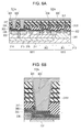
Figs. 8A and 8B are schematic cross-sectional views of a solid-state image pickup device according to a first example not forming part of the claimed invention . -
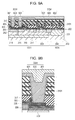
Figs. 9A and 9B are schematic cross-sectional views illustrating a solid-state image pickup device according to a third embodiment. -
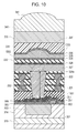
Fig. 10 is a schematic cross-sectional view of a solid-state image pickup device according to a second example being useful to understand the present invention. -
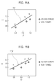
Figs. 11A and 11B are graphs illustrating the second example. -
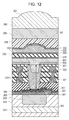
Fig. 12 is a schematic cross-sectional view illustrating a modification of the second example. -
Fig. 13 is a schematic view illustrating a high-density plasma-enhanced chemical vapor deposition apparatus. -
Fig. 14 is a schematic view of a solid-state image pickup device and an image pickup system. -
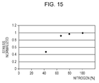
Fig. 15 is a graph illustrating a third example being useful to understand the present invention. - One disclosed aspect of the present invention relates to a method for manufacturing a solid-state image pickup device according to claim 4. Another aspect of the present invention relates to a solid-state image pickup device according to
claims 1 or 2. - The structure may provide the solid-state image pickup device in which an embedded high-refractive-index member has high adhesion and thus is less likely to be detached. It is possible to embed the high-refractive-index member without forming a void. Furthermore, it is possible to inhibit the deformation of a wafer due to the internal stress generated in the high-refractive-index member.
- The term "opening" used here includes the case where an opening passes through an insulating film and where an opening do not pass therethrough (depression), and may also be referred to as a "hole". As a structure including the opening, a structure including a waveguide is described in embodiments. Another structure may also be used. In embodiments and examples described below, a solid-state image pickup device including the structure is exemplified. Common semiconductor devices may also have the structure. In the following description, a method for manufacturing a structure that may be produced by a common technique for producing a semiconductor, and details of the structure may be omitted. Hereinafter, descriptions will be given in detail with reference to the attached drawings.
- In this embodiment, a solid-state image pickup device is exemplified as a semiconductor device. A method for manufacturing a solid-state image pickup device will be described with reference to
Figs. 1 to 5B and14 . First, a solid-state image pickup device according to this embodiment will be described below with reference toFigs. 1 ,2 , and14 . -
Fig. 1 is a circuit diagram illustrating a pixel cell of a solid-state image pickup device according to this embodiment.Fig. 2 is a top view of the pixel cell.Fig. 14 is a block diagram illustrating an image pickup system including the solid-state image pickup device according to aspects of the present invention. InFig. 1 , apixel cell 100 includes four photodiodes (hereinafter, referred to as "PDs") 101 to 104, fourtransfer transistor 105 to 108, areset transistor 110, anamplifying transistor 112, and a floating diffusion node (hereinafter, referred to as an "FD node") 109. - The four
PDs 101 to 104 photoelectrically convert incident light into electric charges corresponding to the quantity of incident light. The fourtransfer transistors 105 to 108 function as transfer units configured to transfer electric charges generated in the fourrespective PDs 101 to 104 into theFD node 109. Specifically, thefirst transfer transistor 105 transfers electric charges generated in thefirst PD 101. Thesecond transfer transistor 106 transfers electric charges generated in thesecond PD 102. Thethird transfer transistor 107 transfers electric charges generated in thethird PD 103. Thefourth transfer transistor 108 transfers electric charges generated in thefourth PD 104. TheFD node 109 is shared among a plurality of photoelectric conversion units. With respect to the amplifyingtransistor 112, a gate is electrically connected to theFD node 109. A drain is supplied with a predetermined voltage from apower supply line 111. A source is electrically connected to anoutput signal line 113. A signal based on the potential of theFD node 109 is fed to theoutput signal line 113. Thereset transistor 110 resets the potential of theFD node 109 to any potential. Simultaneous establishment of electrical continuity between thereset transistor 110 and any of thetransfer transistors 105 to 108 allows the potential of a corresponding one of thePDs 101 to 104 to be reset. Thepower supply line 111 is configured to supply at least two potentials. Setting the potential of theFD node 109 to two values makes it possible to selectively feed a signal to theoutput signal line 113. A terminal 114 is connected to a readout circuit described below. - In the case where a pixel is defined as a repeat unit including at least one photoelectric conversion unit, the
pixel cell 100 includes four pixels inFig. 1 . Thepixel cell 100 may include, for example, a selective transistor and a capacity. While the photodiodes are exemplified as photoelectric conversion units, for example, photogates may be used. - In
Fig. 14 , a solid-stateimage pickup device 1601 includes apixel unit 1611, avertical scanning circuit 1612, tworeadout circuits 1613, twohorizontal scanning circuits 1614, and twooutput amplifiers 1615. A region other than thepixel unit 1611 is referred to as aperipheral circuit portion 1616. - In the
pixel unit 1611, a plurality of pixel cells illustrated inFig. 1 are two-dimensionally arranged. That is, in thepixel unit 1611, the pixels are two-dimensionally arranged. Each of thereadout circuits 1613 includes, for example, a column amplifier, a correlated double sampling (CDS) circuit, and an adding circuit. Eachreadout circuit 1613 reads signals from pixels in a row selected by thevertical scanning circuit 1612 through vertical signal lines and, for example, amplifies and adds the signals. For example, the column amplifier, the CDS circuit, the adding circuit, and so forth are arranged for each pixel column or for a plurality of pixel columns. Thehorizontal scanning circuits 1614 generate signals used to selectively read signals from thereadout circuits 1613. Theoutput amplifiers 1615 amplify and output signals from columns selected by thehorizontal scanning circuits 1614. The structure described above is merely a structural example of the solid-state image pickup device. This embodiment is not limited to the structure. For example, InFig. 14 , eachreadout circuit 1613, eachhorizontal scanning circuit 1614, and eachoutput amplifier 1615 are arranged in a corresponding one of regions located above and below thepixel unit 1611 in order to configure two output paths. Alternatively, three or more output paths may be arranged. - Referring to
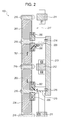
Fig. 2 , a planar layout corresponding toFig. 1 will be described below. InFig. 2 , charge accumulation regions (N-type semiconductor regions) 201 to 204, which are parts of the respective first to fourth PDs, are arranged. Thecharge accumulation regions 201 to 204 are referred to as "first tofourth PDs 201 to 204".Gate electrodes 205 to 208 of the first to fourth transfer transistors corresponding to the first tofourth PDs 201 to 204 are arranged. Afirst FD region 209 and asecond FD region 210 are each arranged as a region corresponding to the FD node illustrated inFig. 1 . Thefirst FD region 209 and thesecond FD region 210 are arranged in different active regions. Charges from the first and second PDs are transferred to thefirst FD region 209. Charges from the third and fourth PDs are transferred to thesecond FD region 210. Thefirst FD region 209, thesecond FD region 210, and agate electrode 212 of the amplifying transistor are electrically connected through a connectingline 213. The connectingline 213 may be formed by the extension of a polysilicon component constituting the gate electrode of the amplifying transistor. Thefirst FD region 209 and the connectingline 213 are connected with a sharedcontact 214. Thesecond FD region 210 and the connectingline 213 are connected with a sharedcontact 215. The term "shared contact" indicates a contact plug that connects semiconductor regions, a semiconductor region and a gate electrode, or gate electrodes, without using a wiring layer. InFig. 2 , thesecond FD region 210 is arranged in an active region common to the source or drain of the reset transistor.Reference numeral 211 denotes the gate electrode of the reset transistor. - Here, regions where the PDs and the sources, drains, and portions functioning as channels of the transistors are arranged are active regions. Other regions are
element isolation regions 217.Potential barriers 216 composed of semiconductor regions that are effective against signal carriers are arranged between adjacent PDs and between adjacent gate electrodes in the active regions. Thepotential barriers 216 serve as element isolation regions that inhibit the transfer of charge carriers between adjacent PDs. In the case where the potential barriers are composed of P-type semiconductor regions, the potential barriers are effective against electrons. In the case where the potential barriers are composed of N-type semiconductor regions, the potential barriers are effective against holes. - A method for manufacturing such a solid-state image pickup device will be described with reference to
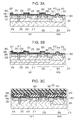
Figs. 3A to 5B. Figs. 3A to 5B are schematic cross-sectional views taken along line III-III, IV-IV, and V-V inFig. 2 . Specifically,Figs. 3A to 5B are cross-sectional views of the second and third PDs in the pixel cell, anytransistor 303 in the pixel cell, and anytransistor 304 in the peripheral circuit portion taken along line III-III, IV-IV, and V-V inFig. 2 . The foregoing components are designated using the same reference numerals, and descriptions are not redundantly repeated. Furthermore, detailed descriptions of steps that can be performed by common semiconductor techniques are omitted. - Referring to
Fig. 3A , a step of preparing a semiconductor substrate including elements will be described below. Asemiconductor substrate 301 prepared is composed of silicon and has a main face (surface) 302. Thesemiconductor substrate 301 includes two N-type semiconductor regions transistor 303 in the pixel cell, and thetransistor 304 in the peripheral circuit portion. Electrons are collected in the N-type semiconductor regions type semiconductor regions charge accumulation regions Fig. 3A , thetransistor 303 in the pixel unit has N-type source and drainregions 309 and agate electrode 308. An N-type semiconductor region 314 is arranged below thecharge accumulation regions type semiconductor region 314 has a lower impurity concentration than the charge accumulation regions and partially constitutes the photoelectric conversion unit together with the charge accumulation regions. A P-type semiconductor region 315 serving partly as the photoelectric conversion unit is arranged below the N-type semiconductor region 314. A P-type semiconductor region 316 is arranged below the source and drainregions 309 of thetransistor 303 and thesecond FD region 210. As thetransistor 304 in the peripheral circuit portion, transistors constituting a CMOS circuit are arranged. In this embodiment, however, only an N-type transistor is illustrated. Thetransistor 304 in the peripheral circuit portion has N-type source and drainregions 311 arranged in a P-type semiconductor region 313 and has agate electrode 310 arranged on themain face 302 of the semiconductor substrate between the source and drain regions. Thesemiconductor substrate 301 including these elements is prepared. Note that in each of the drawings, gate insulating films are not illustrated. -
Fig. 3A illustrates a step of forming insulating films on the elements arranged on the semiconductor substrate. In thepixel unit 1611, an insulating film (not illustrated) composed of silicon oxide, an insulatingfilm 305 composed of silicon nitride, and an insulatingfilm 306 composed of silicon oxide are stacked in that order from themain face 302 side. These films may be formed by plasma-enhanced chemical vapor deposition (hereinafter, referred to as "CVD"). - The
transistor 304 has aside spacer 312 on the side wall of thegate electrode 310. The source and drainregions 311 have a lightly doped drain (LDD) structure (not illustrated). Theside spacer 312 has a laminated structure including a silicon oxide film, a silicon nitride film, and a silicon oxide film. These films may be formed by plasma-enhanced CVD. These films constituting theside spacer 312 may be the same as the insulating film (not illustrated), the insulatingfilm 305, and the insulatingfilm 306 formed in thepixel unit 1611. - In
Fig. 3A , an insulatingfilm 307 composed of silicon nitride is formed over thepixel unit 1611 and theperipheral circuit portion 1616 by, for example, low-pressure plasma-enhanced CVD (LP-CVD). Here, before the formation of the insulatingfilm 307, a film (not illustrated) composed of silicon oxide may be formed over thepixel unit 1611 and theperipheral circuit portion 1616 by plasma-enhanced CVD. This is because the formation of the film prevents exposure of themain face 302 of the semiconductor substrate in the source and drainregions 311 of thetransistor 304 in the peripheral circuit portion. - Referring to
Fig. 3B , the insulatingfilm 307 formed over thepixel unit 1611 and theperipheral circuit portion 1616 is processed by common lithography and etching techniques into a desired pattern to form insulatingfilms 317 and an insulatingfilm 318. The insulatingfilms 317 extend from portions above thecharge accumulation regions pixel unit 1611, the insulatingfilm 307 illustrated inFig. 3A is removed by etching. In theperipheral circuit portion 1616, the insulatingfilm 307 illustrated inFig. 3A is not etched away and is formed into the insulatingfilm 318. - Referring to
Fig. 3C , a plurality of interlayer insulatingfilms 319, contact plugs 320, afirst wiring layer 321, asecond wiring layer 322 including via plugs are formed on the structure illustrated inFig. 3B . Here, plural contacts and plural lines of the wiring layers are arranged. In the pluralinterlayer insulating films 319, insulating films composed of silicon oxide and insulating films composed of silicon nitride are alternately stacked. Each of the insulating films composed of silicon oxide is formed by plasma-enhanced CVD so as to have a thickness of 120 nm to 1000 nm. Each of the insulating films composed of silicon nitride is formed by plasma-enhanced CVD so as to have a thickness of 10 nm to 200 nm. Thus, most of the pluralinterlayer insulating films 319 are composed of silicon oxide. The plural insulating films composed of silicon nitride function as etch stop films at the time of the formation of the wiring layers and the via plugs and as diffusion preventing films configured to prevent diffusion of metals constituting the wiring layers. The pluralinterlayer insulating films 319 will serve as claddings of waveguides to be formed. - The contact plugs 320 are mainly composed of tungsten. The
first wiring layer 321 and thesecond wiring layer 322 formed integrally with the via plugs are mainly composed of copper. Thefirst wiring layer 321 is formed by a single damascene process. Thesecond wiring layer 322 is formed by a dual damascene process. The contact plugs, the via plugs, and conductive patterns of the wiring layers each include a barrier metal. The first and second wiring layers may be composed of aluminum and formed by patterning instead of the damascene processes. - In
Fig. 3C , among the plural insulating films composed of silicon nitride, the insulating films in contact with the upper faces of the first and second wiring layers function as diffusion preventing films configured to prevent diffusion of a metal, i.e., copper. The insulating films arranged on the lower faces of the first and second wiring layers function as etch stop films when the first and second wiring layers are formed by the damascene processes. The thickness of the insulating films functioning as the etch stop films is smaller than that of the insulating films functioning as the diffusion preventing films. In the damascene processes, a step of forming a groove for a line or a groove for a line and a via plug is performed. When the groove is formed by etching, the etch stop film may be arranged to control the shape of the groove. Thus, the insulating films functioning as the etch stop films are arranged on the lower faces of the first and second wiring layers. The etch stop films are removed in forming the grooves. Hence, the lower faces of the etch stop films are flush with or above the lower faces of the first and second wiring layers.
Alternatively, a wafer in which the structure illustrated inFig. 3C has been formed is obtained, and then the subsequent step of forming an opening may be performed. - Next,
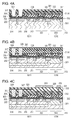
openings 323 are formed in the pluralinterlayer insulating films 319 illustrated inFig. 3C , thereby forming a structure illustrated inFig. 4A . A photoresist pattern (not illustrated) having openings in regions corresponding to the photoelectric conversion unit is formed on the pluralinterlayer insulating films 319. Etching is performed with the photoresist pattern as a mask. For example, anisotropic etching is performed as the etching. Specifically, the plural interlayer insulating films are subjected to plasma etching treatment until the insulatingfilms 317 are exposed. The insulatingfilms 317 reduce plasma damage to the photoelectric conversion unit during etching and also function as etch stop films. The insulating film (not illustrated) composed of silicon oxide and the insulatingfilms films 317 and themain face 302 of the semiconductor substrate function as antireflection coating films for light incident on the photoelectric conversion unit. - The
openings 323 illustrated inFig. 4A is filled with a transparent material having a higher refractive index than the pluralinterlayer insulating films 3191 serving as claddings, thereby forming portions to be formed into cores of waveguides. Here, silicon nitride having a higher refractive index than silicon oxide that mainly constitutes the pluralinterlayer insulating films 3191 is deposited in the openings. Specifically, silicon nitride is deposited by high-density plasma-enhanced CVD (hereinafter, referred to as "HDP-CVD") on the entire face of the substrate to fill theopenings 323 with silicon nitride. The HDP-CVD is performed with a high-density plasma-enhanced CVD apparatus illustrated inFig. 13 . An unnecessary portion of the resulting silicon nitride film formed on, for example, a portion on the pluralinterlayer insulating films 3191 other than theopenings 323 is removed by chemical mechanical polishing (hereinafter, referred to as "CMP") or plasma etching. This step planarizes the surface of the silicon nitride film. Thereby, high-refractive-index members 324 are formed in theopenings 323 through these steps. Waveguides include the pluralinterlayer insulating films 3191 and the high-refractive-index members 324. Here, in this embodiment, CMP is performed to remove and planarize the silicon nitride film. Part of the silicon nitride film on the pluralinterlayer insulating films 3191 is left, thus forming an insulatingfilm 325 over the high-refractive-index members 324 and the upper face of the pluralinterlayer insulating films 3191, the insulatingfilm 325 having a thickness of about 100 nm to about 500 nm. The presence of the silicon nitride film reduces plasma damage to the wiring layers. An insulatingfilm 326 composed of silicon oxynitride is formed on the surface of the insulatingfilm 325. The insulatingfilm 326 is formed by plasma-enhanced CVD so as to have a thickness of about 50 nm to about 150 nm. - After the step illustrated in
Fig. 4B , desired regions of the insulatingfilms films opening 329. However, at least a region where the via plugs are arranged may be removed by etching. The removal is performed by anisotropic etching, for example, plasma etching. This step forms the insulatingfilms films opening 329. Subsequently, an insulatingfilm 330 is formed so as to fill theopening 329 and cover the insulatingfilms film 330 is composed of, for example, silicon oxide and may be formed by plasma-enhanced CVD. A viaplug 331 is formed so as to pass through the insulatingfilm 330 and some of the pluralinterlayer insulating films 319 arranged on thesecond wiring layer 322. The viaplug 331 is composed of, for example, tungsten and includes a barrier metal, for example, titanium or titanium nitride. - A
third wiring layer 333 is formed on the viaplug 331, providing a structure illustrated inFig. 4C . Thethird wiring layer 333 is composed of an electric conductor mainly containing, for example, aluminum and is formed by patterning. Here, thethird wiring layer 333 also functions as a light-shielding film for the peripheral circuit portion. InFig. 4C , an insulating film to be formed into an insulatingfilm 334 and an insulating film to be formed into an insulatingfilm 335 are formed in that order. The insulating film to be formed into the insulatingfilm 334 is composed of silicon oxynitride formed by plasma-enhanced CVD. The insulating film to be formed into the insulatingfilm 335 is composed of silicon nitride formed by plasma-enhanced CVD. A lens-shaped photoresist is formed on the insulating film to be formed into the insulatingfilm 335. Etching is performed with the photoresist as a mask to form lenses in the insulating film to be formed into the insulatingfilm 335. An insulating film to be formed into an insulatingfilm 336 is formed on the lenses. Removal of the three insulating films in a region corresponding to an input or output pad provides a structure illustrated inFig. 5A . Here, the insulatingfilm 335 serves as a lens layer includingintra-layer lenses 337. The insulatingfilms film 335. - After the step illustrated in
Fig. 5A , aplanarizing layer 338 composed of a resin, acolor filter layer 339 including a color filter corresponding to a plurality of colors, and amicrolens layer 340 includingmicrolenses 341 are formed in that order, providing a structure illustrated inFig. 5B . - As described above, it is possible to produce a solid-state image pickup device by the procedure illustrated in
Figs. 3A to 5B . Note thatFigs. 3A to 5B illustrate a portion on the main face side of thesemiconductor substrate 301. - In the method for manufacturing a solid-state image pickup device described above, the process of forming the high-refractive-
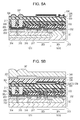
index members 324 illustrated inFig. 4B is a characteristic feature of this embodiment. This step will be described in detail below with reference toFigs. 6A, 6B , and13 . - In this embodiment, the high-refractive-
index members 324 are formed by the two-stage process.Fig. 6A is a schematic cross-sectional view of a solid-state image pickup device corresponding toFig. 4B .Fig. 6B is an enlarged fragmentary schematic cross-sectional view of the structure illustrated inFig. 6A . InFigs. 6A and 6B , elements equal to elements inFig. 4B are designated using the same reference numerals, and descriptions are not redundantly repeated. As illustrated inFigs. 6A and 6B , the high-refractive-index members 324 and the insulatingfilm 325 inFig. 4B correspond to high-refractive-index members 324a and an insulatingfilm 325a, respectively, inFigs. 6A and 6B . The high-refractive-index members 324a and the insulatingfilm 325a are each formed of two members. InFigs. 6A and 6B , afirst member 601 and an insulatingfilm 602 are formed along side walls of theopenings 323 illustrated inFig. 4A and cover the pluralinterlayer insulating films 3191. Asecond member 603 and an insulatingfilm 604 cover thefirst member 601 and the insulatingfilm 602. Each of the high-refractive-index members 324a includes thefirst member 601 and thesecond member 603. The insulatingfilm 325a corresponding to the insulatingfilm 325 illustrated inFig. 4A includes the insulatingfilm 602 and the insulatingfilm 604. A method for forming the high-refractive-index members 324a will be described in detail below with reference toFig. 6B . - A high-density plasma-enhanced CVD apparatus to form the high-refractive-
index members 324a will be described with reference toFig. 13 . The high-density plasma-enhanced CVD apparatus is one in which a gas is formed into a dense plasma using a radio-frequency field or a magnetic field to deposit a film.Fig. 13 is a schematic view illustrating a high-density plasma-enhancedCVD apparatus 1500 using a radio-frequency field. The high-density plasma-enhancedCVD apparatus 1500 includes achamber 1506, astage 1503 equipped with a temperature control mechanism, a radio-frequency power source 1501 connected to a first electrode, and a radio-frequency power source 1502 connected to the stage (second electrode). Asemiconductor wafer 1504 is placed on thestage 1503. Radio-frequency powers of the upper radio-frequency power source 1501 and the lower radio-frequency power source 1502 may be individually set. When a film is formed, a desired gas is fed from afeed port 1505 and allowed to react. The high-density plasma-enhanced CVD is performed while a sputtering effect and a deposition effect are adjusted. By controlling the radio-frequency powers of the upper and lower radio-frequency power sources, the gas, the temperature of the wafer, and so forth, the ratio of the sputtering effect to the deposition effect is adjusted. - A method for forming the high-refractive-index members according to this embodiment includes a first step of forming the first member and a second step of forming the second member. The second step is performed under conditions in which the ratio of the sputtering effect to the deposition effect is higher than that in the first step. The term "deposition effect" used here indicates a state in which a film of a desired species is grown by CVD. The term "sputtering effect" indicates a state in which an underlying film is subjected to sputtering by bombardment with a plasma or a species.
- The first member formed under the conditions has higher adhesion to the side walls and bottom faces of the
openings 323 and theinterlayer insulating films 3191 illustrated inFig. 4A than the second member, thus inhibiting the detachment of the first member to form a high-refractive-index member. Furthermore, a stress generated in the second member is reduced, thus inhibiting the deformation of the wafer. In the high-density plasma-enhanced CVD, a member formed under conditions in which the deposition effect is high has a high density and high adhesion to an underlying film. That is, in the first step, the film having high adhesion to the underlying film is formed. Then in the second step, the high-refractive-index members are formed under conditions in which the openings are easily filled. Note that a film having high adhesion to an underlying film is highly likely to have a high stress. In the case where an opening is filled with such a film, the thickness of the film is increased, so that a wafer is likely to deform. In the method according to this embodiment, it is possible to reduce the detachment and inhibit the deformation of the wafer. - In the first step, a mixed gas that contains a silicon-containing gas, nitrogen, a nitrogen-containing gas, and an inert gas is fed, and a radio-frequency field is applied from the radio-
frequency power source 1501. In the second step, a mixed gas that contains a silicon-containing gas, nitrogen, a nitrogen-containing gas, and an inert gas is fed, and radio-frequency fields are applied from the radio-frequency power sources - Examples of the silicon-containing gas include silane, tetraethoxysilane (TEOS), trimethylsilane, and tetramethylsilane. An example of the nitrogen-containing gas is ammonia. Examples of the inert gas include argon and helium. In this embodiment, the mixed gas in each of the first and second steps includes silane, nitrogen, ammonia, and argon.
- The radio-
frequency power source 1501 supplies a radio frequency of 800 kHz at a radio-frequency power of 1000 to 7000 W. The radio-frequency power source 1502 supplies a radio frequency of 13.56 MHz at a radio-frequency power of 0 to 5000 W. According to this embodiment, in the first step, the radio-frequency power of the radio-frequency power source 1501 is 5000 W, and the radio-frequency power of the radio-frequency power source 1502 is 0 W. In the second step, the radio-frequency power of the radio-frequency power source 1501 is 5000 W, and the radio-frequency power of the radio-frequency power source 1502 is 3000 W. In the first step, the radio-frequency field is applied only to thesemiconductor wafer 1504, i.e., only to the electrode adjacent to the front face of the semiconductor substrate. That is, in the first step, the ratio of the radio-frequency power applied to the electrode adjacent to the front face of the semiconductor substrate to the radio-frequency power applied to the electrode adjacent to the back face of the semiconductor substrate is high compared with the second step. - That is, the second step is performed under conditions in which the ratio of the sputtering effect to the deposition effect is high compared with the first step. The conditions are, for example, ones in which in the second step, the ratio of a radio-frequency power applied to the electrode adjacent to the back face of the semiconductor substrate to a radio-frequency power applied to the electrode adjacent to the front face of the semiconductor substrate is high compared with the first step. In other words, the ratio in the second step is higher than that in the first step. Furthermore, a high proportion of the inert gas is suitable for the conditions. In this case, an excessively high proportion of the inert gas leads to an excessively high sputtering effect. Thus, the insulating film, i.e., the underlying film, on the side walls of the
openings 323 illustrated inFig. 4A may be removed. Consequently, for example, the ratio of argon to silane in the second step may be in the range of 1.0 to 6.0. - Under the conditions described above, after the first step of forming the
first member 601 in theopenings 323 illustrated inFig. 4A , the second step of forming thesecond member 603 is performed, thereby forming the high-refractive-index members 324a. The first member has a thickness of 10 nm to 50 nm. The reason for this is as follows: A thickness of the first member of less than 10 nm does not result in sufficient adhesion. A thickness exceeding 50 nm results in the deformation of the wafer due to the stress in the member. - As described above, it is possible to form the high-refractive-
index members 324a that are less likely to be detached from the underlying film by the production method according to this embodiment. It is also possible to reduce the stress in the high-refractive-index members and thus reduce the deformation of the wafer. - The method may further include a third step of forming a third member between the first step and the second step. In the third step, the ratio of the sputtering effect to the deposition effect, for example, the ratio of a radio-frequency power applied to the electrode adjacent to the back face to a radio-frequency power applied to the electrode adjacent to the front face of the semiconductor substrate, is set under conditions intermediate between the conditions in the first step and the conditions in the second step. In this way, the step may be performed under the conditions intermediate between the conditions in the first step and the conditions in the second step, thereby continuously forming the high-refractive-index members. In the foregoing descriptions, the first member, the second member, and so forth are used for simplicity. Alternatively, an integrated member may be provided as a final structure. The cone angle of each opening 323 illustrated in
Fig. 4A is not limited to the angle in this embodiment. - This embodiment is different from the first embodiment in that the high-refractive-
index members 324 are formed in one step. The other portions of the structure and the production method are the same as those in the first embodiment.Fig. 7A corresponds toFig. 6B and is an enlarged fragmentary schematic cross-sectional view of a solid-state image pickup device corresponding to that illustrated inFig. 4B . As illustrated inFig. 7A , a high-refractive-index member 324b is formed of asingle member 701. In this embodiment, themember 701 is composed of a material having properties that exhibit aspectrum 702 depicted inFig. 7B . The use of the material inhibits the formation of voids when theopenings 323 illustrated inFig. 4A are filled with a high-refractive-index material. A graph depicted inFig. 7B will be described in detail below. -
Fig. 7B is a graph illustrating analytical results by Fourier transform infrared spectroscopy (hereinafter, referred to as "FT-IR"). The horizontal axis represents the wavenumber. The vertical axis represents the absorbance. In the graph, apeak 704 indicates the presence of N-H bonds. Apeak 705 indicates the presence of Si-H bonds. Apeak 706 indicates the presence of Si-N bonds. Thespectrum 702 exhibits the analytical result of themember 701. A spectrum 703 exhibits the analytical result of a comparable member that causes the formation of a void in filling theopenings 323 illustrated inFig. 4A . Silicon nitride formed by plasma-enhanced CVD contains Si, H, and N. Thespectrum 702 has the peak 704 that indicates N-H bonds and demonstrates that many N-H bonds are contained. The spectrum 703 demonstrates that the amount of the Si-H bonds is greater than that of the N-H bonds. To inhibit the formation of voids, the silicon nitride has a ratio of the N-H bonds to the Si-H bonds, i.e., N-H bonds/Si-H bonds, of 1.0 to 10. - The
member 701 is formed by high-density plasma-enhanced CVD under the conditions used in the second step according to the first embodiment. To increase the number of the N-H bonds, known conditions may be used in which a film containing a large number of N-H bonds is formed by common high-density plasma-enhanced CVD. For example, the conditions are used in which the ratio of the sputtering effect to the deposition effect is high in the second step according to the first embodiment. In addition, the proportion of nitrogen in the mixed gas described in the first embodiment may be increased. For example, the proportion of nitrogen is set to 1.2 to 2.0 times the silicon-containing gas, 2.0 to 4.0 times the nitrogen-containing gas, and 2.0 to 4.0 times the inert gas. In the case where the N-H bonds fall within the range described above, it is possible to fill the openings with the high-refractive-index member without forming a void. It is also possible to control the internal stress within an appropriate range and thus inhibit the deformation of the wafer. Hence, this embodiment may be suitable for the structure in which the insulatingfilm 327 is arranged on the high-refractive-index members 324 as illustrated inFig. 5B . - To improve the adhesion to the insulating films to be formed into claddings, the high-refractive-
index members 324 may be formed by the two steps as in the first embodiment. - This example not forming part of the claimed invention is different from the first embodiment in that the high-refractive-
index members 324 are formed in one step. The other portions of the structure and the production method are the same as those in the first embodiment.Fig. 8A corresponds toFig. 6B and is an enlarged fragmentary schematic cross-sectional view of a solid-state image pickup device corresponding to that illustrated inFig. 4B . As illustrated inFig. 8A , a high-refractive-index member 324c is formed of a single member 803. InFig. 8A , one of theopenings 323, which are illustrated inFig. 4A and are regions where the high-refractive-index members 324c are formed, has abottom face 801, anupper plane 802 including the upper face of the pluralinterlayer insulating films 3191 in a region surrounding theopenings 323 illustrated inFig. 4A , and aside face 805. Here, a direction perpendicular to thebottom face 801 is defined as a direction 804. A direction parallel to thebottom face 801 is defined as adirection 806. Thebottom face 801 is parallel to themain face 302 of the substrate. - In this example a film to be formed into the member 803 is formed by high-density plasma-enhanced CVD to fill the
corresponding opening 323 under conditions such that the deposition rate of the film to be formed into the member 803 satisfies the relationship described below. The conditions are such that the deposition rate from thebottom face 801 in the direction 804 is 1.5 to 10 times the deposition rate from theside face 805 in thedirection 806. For example, the film is formed under the conditions used in the second step according to the first embodiment. Unlike amember 807 illustrated inFig. 8B , a protrudingportion 809 is not formed under the conditions.Fig. 8B illustrates a filling process under conditions in which a void is formed. In this case, the upper portion of the opening will be clogged with the protrudingportion 809 to form a void. In the production method according to this example however, it is possible to form a waveguide while the formation of a void is inhibited. - This embodiment is different from the first embodiment in that the high-refractive-
index members 324 and the insulatingfilm 325 are formed in three steps (with three members). The other portions of the structure and the production method are the same as those in the first embodiment.Fig. 9A is a schematic cross-sectional view of a solid-state image pickup device corresponding to that illustrated inFig. 6A .Fig. 9B is an enlarged fragmentary schematic cross-sectional view of a solid-state image pickup device corresponding to that illustrated inFig. 6B . As illustrated inFig. 9A , a high-refractive-index member 324d and an insulatingfilm 325d each include three members. The high-refractive-index member 324d includes thefirst member 601, thesecond member 603, and athird member 901. The insulatingfilm 325d includes the insulatingfilm 602, an insulatingfilm 903, and an insulatingfilm 902. The insulatingfilm 903 is a member in which the insulatingfilm 604 illustrated inFig. 6A is partially removed. - In a production method illustrated in
Fig. 9A , after the first step and the second step described in the first embodiment are performed, an etching step of partially removing the insulatingfilm 604, illustrated in theFig. 6A , formed in the second step is performed by etching. Here, the insulatingfilm 604 illustrated inFig. 6A is formed into the insulatingfilm 903. Then a third step of forming thethird member 901 and the insulatingfilm 902 is performed under the same conditions as those in the second step. In this way, the etching step is performed in the middle of the process. This facilitates planarization after the formation of the high-refractive-index member 324d and the insulatingfilm 325d. Partial removal of the insulatingfilm 604 illustrated inFig. 6A results in a reduction in stress, thus reducing the occurrence of cracking and the detachment of the high-refractive-index member. The three members may be integrated. - According to this example being useful to understand the present invention, the shape of each of the
openings 323 illustrated inFig. 4A will be described below with reference toFig. 10. Fig. 10 is an enlarged view of a structure corresponding to that inFig. 5B . Common elements are designated using the same reference numerals, and descriptions are not redundantly repeated. The other portions of the structure and the production method are the same as those in the first embodiment. - The shape of each opening 323 illustrated in
Fig. 4A , i.e., the shape of a high-refractive-index member 324e, is defined by abottom face 1001, anupper face 1003, and aside face 1002 that connects thebottom face 1001 and theupper face 1003. Thebottom face 1001 and theupper face 1003 are parallel to themain face 302 including a light receiving face. The widest dimension of thebottom face 1001 is represented by L1. The widest dimension of theupper face 1003 is represented by L2. The length of a line segment that connects theupper face 1003 and thebottom face 1001 is represented by height H. The angle of inclination of theside face 1002 to a plane including thebottom face 1001 is represented by α. Height H is perpendicular to themain face 302. The shape of the high-refractive-index member 324e satisfies the following relationships: L1 < L2, H/L2 ≤ 2, and 72.8° < α < 90°. The relationships lead to the formation of the high-refractive-index member 324e without forming a void. The relationships will be described below with reference toFigs. 11A and 11B . -
Fig. 11A is a graph illustrating the presence or absence of the formation of a void, the vertical axis representing L1, and the horizontal axis representing L2.Fig. 11B is a graph illustrating the presence or absence of the formation of a void, the vertical axis representing H, and the horizontal axis representing L2. Each value is a ratio with respect to a given value. The measurement is performed on a structure in which the high-refractive-index members according to the first embodiment are arranged. Boundaries are found fromFigs. 11A and 11B . Aboundary line 1101 depicted inFig. 11A indicates that L1 = L2. Aboundary line 1102 depicted inFig. 11B indicates that H/L2 = 2. In regions where L1 < L2 and H/L2 ≤ 2 in the graphs, it is possible to form the high-refractive-index member 324e without forming a void. - It is possible to appropriately combine this example with the first to third embodiments and first example . For example,
Fig. 12 illustrates a structure in which the structure according to this example is combined with the structure according to the third embodiment. InFig. 12 , the structure has the cone angle α illustrated inFig. 10 and the first to third members and the insulating film illustrated inFigs. 9A and 9B . This structure makes it possible to further reduce the formation of voids. - The difference between this example being useful to understand the present invention and the first embodiment is the method for forming the
second member 603 of the high-refractive-index members 324a (seeFig. 6B ) (second step). The other portions of the structure and the production method are the same as those in the first embodiment. - Here, the relationship between the flow rate of nitrogen and the stress in the high-refractive-index member will be described with reference to
Fig. 15 . InFig. 15 , the horizontal axis represents the flow rate (sccm) of nitrogen in the chamber of the CVD apparatus when the high-refractive-index member is formed. In this case, the flow rate is normalized in such a manner that a reference flow rate is defined as 100% when the opening can be filled with the high-refractive-index member. The vertical axis represents the stress in the high-refractive-index member. The stress in the high-refractive-index member is measured by uniformly forming the high-refractive-index member on a flat substrate and measuring the stress with a stress measurement device. In this case, the stress is normalized in such a manner that a reference stress in the high-refractive-index member is defined as 1 when a nitrogen flow rate at which the opening can be filled with the high-refractive-index member is set.Fig. 15 demonstrates that a lower nitrogen flow rate results in a lower stress in the high-refractive-index member in the second step according to the first embodiment. Note that a reduction in the flow rate of nitrogen is offset by an increase in the flow rate of helium. - Table 1 illustrates the success or failure of filling at various pressures (mTorr) in the chamber. Evaluation criteria are described below.
- Good: The openings were filled with the high-refractive-index member.
- Bad: The openings were not filled with the high-refractive-index member.
- Table 1 demonstrates that the pressure in the chamber is preferably in the range of 3 mTorr to 10 mTorr and more preferably 6 mTorr to 9 mTorr.
-
Fig. 15 and Table 1 demonstrate the following: The use of helium in addition to nitrogen makes it possible to fill the openings with a low-stress film. A pressure in the chamber of 3 mTorr to 10 mTorr facilitates the filling. In the case where the flow rate of nitrogen is reduced, the flow rate of helium is increase, and the pressure in the chamber is in the range of 3 mTorr to 10 mTorr, it is possible to fill the openings with a silicon nitride film having a lower stress. - The difference between this example not forming part of the claimed invention and the first embodiment is the method for forming the
first member 601 of the high-refractive-index members 324a (seeFig. 6B ) (first step). The other portions of the structure and the production method are the same as those in the first embodiment. In this example in the first step of forming the high-refractive-index members 324a, a silicon nitride film is formed by parallel-plate plasma-enhanced CVD, thereby providing the first member. In the first step according to this example a silicon-containing gas, nitrogen, and a nitrogen-containing gas are fed, and the silicon nitride film is formed. The silicon nitride film may have a thickness of 10 nm or more in the same way as in the first embodiment. A thickness of less than 10 nm does not result in sufficient adhesion. Thus, the resulting high-refractive-index members may be detached in the subsequent step. The second step is performed by high-density plasma-enhanced CVD in the same way as in the first embodiment, thereby filling the openings. In this example the silicon nitride film formed by the parallel-plate plasma-enhanced CVD in the first step has a low stress compared with the silicon nitride film formed by the high-density plasma-enhanced CVD in the first step according to the first embodiment. This allows the high-refractive-index members 324a to have a reduced stress, thereby inhibiting the detachment of the high-refractive-index members. Image Pickup System - The configuration of an image pickup system will be described with reference to
Fig. 14. Fig. 14 is a block diagram of a solid-state image pickup device and an image pickup system. Animage pickup system 1600 includes the solid-stateimage pickup device 1601 and asignal processing unit 1602 into which an electric signal is fed from the solid-stateimage pickup device 1601 and which processes the electric signal. Specifically, electric signals are fed from OUT1 and OUT2 of the solid-stateimage pickup device 1601 to IN of thesignal processing unit 1602. Image signals, driving signals, and control signals are fed from OUT3 of thesignal processing unit 1602 in response to the results of the processing of the electric signals. As the electric signals, current signals, voltage signals, analog signals, or digital signals may be used. The solid-stateimage pickup device 1601 may be used for image sensors, focus detection sensors, light-quantity detection sensors, and so forth. Thesignal processing unit 1602 processes input electric signals and feeds image signals, driving signals to drive a lens, and control signals to control an exposure time. The image pickup system provides suitable image signals or control signals that may be used for control. - As has been described above, according to these embodiments, it is possible to achieve at least one of improvement in adhesion, the inhibition of the deformation of the wafer, and the reduction of the formation of voids. These embodiments may be appropriately modified and combined with each other.
- While the present invention has been described with reference to exemplary embodiments, it is to be understood that the invention is not limited to the disclosed exemplary embodiments but by the scope of the appended claims.
| Pressure (mTorr) | 2.8 | 3.0 | 6.0 | 9.0 | 10.0 | 12.0 | 13.0 |
| Success or failure of filling | bad | good | good | good | good | bad | bad |
Claims (6)
- A solid-state image pickup device comprising:a substrate (301) including a photoelectric conversion unit (101 to 104), anda waveguide arranged on the substrate, the waveguide corresponding to the photoelectric conversion unit and including a core (324b, 701) made of HDP silicon nitride and a cladding (3191),wherein the core consists of a silicon nitride member (324b), characterized in thatthe silicon nitride member contains Si-H bonds and N-H bonds, and has a ratio of the N-H bonds to the Si-H bonds, i.e., N-H bonds/Si-H bonds, of 1.0 to 10.
- A solid-state image pickup device comprising:a substrate (301) including a photoelectric conversion unit (101 to 104), anda waveguide arranged on the substrate, the waveguide corresponding to the photoelectric conversion unit and including a core (324a) made of HDP silicon nitride and a cladding (3191),characterized in thatthe core comprises a first silicon nitride member (601) and a second silicon nitride member (603),the core comprises the first silicon nitride member arranged along and adhering with a first side to sidewalls of an opening (323) of the cladding;the second silicon nitride member covers the first silicon nitride member on a second side opposite to the first side;the second silicon nitride member contains Si-H bonds and N-H bonds, and has a ratio of the N-H bonds to the Si-H bonds, i.e., N-H bonds/Si-H bonds, of 1.0 to 10; andthe first silicon nitride member has a thickness of 10 nm to 50 nm.
- The solid-state image pickup device according to any of Claims 1 to 2, wherein the silicon nitride of the core extends to on the cladding on a side opposite to the substrate.
- A method for manufacturing a solid-state image pickup device that includes
a substrate (301) including a photoelectric conversion unit, and
a waveguide arranged on the substrate, the waveguide corresponding to the photoelectric conversion unit and including core (324a) made of silicon nitride and a cladding, the method comprising:a first step and a second step,wherein in the first step a first silicon nitride member (601) of the core is formed along and adhering to sidewalls of an opening (323) of the cladding by high-density plasma-enhanced chemical vapor deposition, and in the second step a second silicon nitride member (603) of the core is formed in the opening of the cladding on the first silicon nitride member by high-density plasma-enhanced chemical vapor deposition, andwherein in the second step, the second member is formed under conditions in which the ratio of the sputtering effect to the deposition effect is higher than in the first step,the second member contains Si-H bonds and N-H bonds, and has a ratio of the N-H bonds to the Si-H bonds, i.e., N-H bonds/Si-H bonds, of 1.0 to 10; andthe first member has a thickness of 10 nm to 50 nm. - The method according to claim 4, wherein
in the first step and the second step, a mixed gas that contains a silicon-containing gas, nitrogen, a nitrogen-containing gas, and an inert gas is fed. - The method according to any one of claims 4 to 5, wherein
in the first step and the second step, the high-density plasma-enhanced chemical vapor deposition is performed with a high-density plasma-enhanced CVD apparatus having an upper electrode and a lower electrode, wherein the substrate is arranged between the upper electrode and the lower electrode, and
in the second step, high-density plasma-enhanced chemical vapor deposition is performed under a condition in which a ratio of a radio-frequency power of the lower electrode to a radio-frequency power of the upper electrode is higher than that in the first step.
Applications Claiming Priority (2)
| Application Number | Priority Date | Filing Date | Title |
|---|---|---|---|
| JP2011026346 | 2011-02-09 | ||
| JP2011223302A JP5284438B2 (en) | 2011-02-09 | 2011-10-07 | Solid-state imaging device and method for manufacturing solid-state imaging device |
Publications (3)
| Publication Number | Publication Date |
|---|---|
| EP2487715A2 EP2487715A2 (en) | 2012-08-15 |
| EP2487715A3 EP2487715A3 (en) | 2013-02-27 |
| EP2487715B1 true EP2487715B1 (en) | 2015-03-25 |
Family
ID=45463485
Family Applications (1)
| Application Number | Title | Priority Date | Filing Date |
|---|---|---|---|
| EP12151095.2A Not-in-force EP2487715B1 (en) | 2011-02-09 | 2012-01-13 | Solid-state image pickup device and method for manufacturing solid-state image pickup device |
Country Status (7)
| Country | Link |
|---|---|
| US (1) | US9224777B2 (en) |
| EP (1) | EP2487715B1 (en) |
| JP (1) | JP5284438B2 (en) |
| KR (1) | KR101476497B1 (en) |
| CN (1) | CN102637703B (en) |
| BR (1) | BR102012002818A2 (en) |
| RU (1) | RU2497233C2 (en) |
Families Citing this family (8)
| Publication number | Priority date | Publication date | Assignee | Title |
|---|---|---|---|---|
| JP2012182426A (en) * | 2011-02-09 | 2012-09-20 | Canon Inc | Solid state image pickup device, image pickup system using solid state image pickup device and solis state image pickup device manufacturing method |
| US20120267741A1 (en) * | 2011-04-21 | 2012-10-25 | Panasonic Corporation | Solid-state imaging device and method for manufacturing the same |
| US20140186544A1 (en) * | 2013-01-02 | 2014-07-03 | Applied Materials, Inc. | Metal processing using high density plasma |
| JP6136663B2 (en) * | 2013-07-04 | 2017-05-31 | ソニー株式会社 | Solid-state imaging device, manufacturing method thereof, and electronic device |
| JP6465545B2 (en) | 2013-09-27 | 2019-02-06 | ソニー株式会社 | Imaging device, manufacturing method thereof, and electronic apparatus |
| TWI571626B (en) * | 2015-07-15 | 2017-02-21 | 力晶科技股份有限公司 | Integrated bio-sensor with nanocavity and fabrication method thereof |
| JP2017069553A (en) | 2015-09-30 | 2017-04-06 | キヤノン株式会社 | Solid-state imaging device, method of manufacturing the same, and camera |
| US10375338B2 (en) * | 2017-02-01 | 2019-08-06 | Omnivision Technologies, Inc. | Two stage amplifier readout circuit in pixel level hybrid bond image sensors |
Family Cites Families (20)
| Publication number | Priority date | Publication date | Assignee | Title |
|---|---|---|---|---|
| JPH0745601A (en) * | 1993-07-27 | 1995-02-14 | Fuji Electric Co Ltd | Method and apparatus for plasma cvd |
| JPH0992813A (en) * | 1995-09-27 | 1997-04-04 | Sony Corp | Solid state image pickup device and its manufacture |
| KR20010051285A (en) * | 1999-10-28 | 2001-06-25 | 윌리엄 비. 켐플러 | Hdp capping layer or polish layre over hsq/peteos ild stack to enhance planarity and gap-fill |
| US20030110808A1 (en) * | 2001-12-14 | 2003-06-19 | Applied Materials Inc., A Delaware Corporation | Method of manufacturing an optical core |
| JP4427949B2 (en) * | 2002-12-13 | 2010-03-10 | ソニー株式会社 | Solid-state imaging device and manufacturing method thereof |
| JP2005251804A (en) * | 2004-03-01 | 2005-09-15 | Canon Inc | Imaging device |
| JP2006120845A (en) * | 2004-10-21 | 2006-05-11 | Canon Inc | Photoelectric converter and its manufacturing method |
| US7592645B2 (en) * | 2004-12-08 | 2009-09-22 | Canon Kabushiki Kaisha | Photoelectric conversion device and method for producing photoelectric conversion device |
| JP2007201162A (en) * | 2006-01-26 | 2007-08-09 | Fujifilm Corp | Solid-state imaging element, and manufacturing method thereof |
| US7524690B2 (en) * | 2006-08-10 | 2009-04-28 | United Microelectronics Corp. | Image sensor with a waveguide tube and a related fabrication method |
| US7973271B2 (en) * | 2006-12-08 | 2011-07-05 | Sony Corporation | Solid-state image pickup device, method for manufacturing solid-state image pickup device, and camera |
| KR20080111624A (en) * | 2007-06-19 | 2008-12-24 | 삼성전자주식회사 | Plasma etching apparatus and chamber cleaning method using plasma etching apparatus |
| JP4852016B2 (en) | 2007-10-29 | 2012-01-11 | 株式会社東芝 | Semiconductor device and manufacturing method thereof |
| US7704897B2 (en) * | 2008-02-22 | 2010-04-27 | Applied Materials, Inc. | HDP-CVD SiON films for gap-fill |
| JP5402083B2 (en) | 2008-09-29 | 2014-01-29 | ソニー株式会社 | SOLID-STATE IMAGING DEVICE, ITS MANUFACTURING METHOD, AND ELECTRONIC DEVICE |
| KR20100037208A (en) | 2008-10-01 | 2010-04-09 | 주식회사 동부하이텍 | Image sensor and fabricating method thereof |
| KR101561862B1 (en) * | 2008-12-26 | 2015-10-21 | 삼성전자 주식회사 | Fabricating method of semiconductor integrated circuit devices |
| JP5644057B2 (en) * | 2009-03-12 | 2014-12-24 | ソニー株式会社 | Solid-state imaging device, manufacturing method thereof, and imaging device |
| JP5434252B2 (en) * | 2009-05-14 | 2014-03-05 | ソニー株式会社 | Solid-state imaging device, manufacturing method thereof, and electronic apparatus |
| JP2010283145A (en) | 2009-06-04 | 2010-12-16 | Sony Corp | Solid-state image pickup element and method of manufacturing the same, electronic apparatus |
-
2011
- 2011-10-07 JP JP2011223302A patent/JP5284438B2/en not_active Expired - Fee Related
-
2012
- 2012-01-13 EP EP12151095.2A patent/EP2487715B1/en not_active Not-in-force
- 2012-02-01 KR KR1020120010273A patent/KR101476497B1/en active IP Right Grant
- 2012-02-02 US US13/365,055 patent/US9224777B2/en not_active Expired - Fee Related
- 2012-02-06 CN CN201210024736.3A patent/CN102637703B/en not_active Expired - Fee Related
- 2012-02-07 BR BRBR102012002818-2A patent/BR102012002818A2/en not_active Application Discontinuation
- 2012-02-08 RU RU2012104496/28A patent/RU2497233C2/en not_active IP Right Cessation
Non-Patent Citations (1)
| Title |
|---|
| J. YOTA ET AL: "Comparison between HDP CVD and PECVD silicon nitride for advanced interconnect applications", PROCEEDINGS OF THE IEEE 2000 INTERNATIONAL INTERCONNECT TECHNOLOGY CONFERENCE (CAT. NO.00EX407), 1 January 2000 (2000-01-01), pages 76 - 78, XP055126578, ISBN: 978-0-78-036327-4, DOI: 10.1109/IITC.2000.854287 * |
Also Published As
| Publication number | Publication date |
|---|---|
| CN102637703A (en) | 2012-08-15 |
| EP2487715A3 (en) | 2013-02-27 |
| EP2487715A2 (en) | 2012-08-15 |
| US20120202310A1 (en) | 2012-08-09 |
| CN102637703B (en) | 2016-03-16 |
| RU2012104496A (en) | 2013-08-20 |
| BR102012002818A2 (en) | 2013-07-23 |
| JP5284438B2 (en) | 2013-09-11 |
| US9224777B2 (en) | 2015-12-29 |
| KR20120092021A (en) | 2012-08-20 |
| RU2497233C2 (en) | 2013-10-27 |
| JP2012182431A (en) | 2012-09-20 |
| KR101476497B1 (en) | 2014-12-24 |
Similar Documents
| Publication | Publication Date | Title |
|---|---|---|
| EP2487715B1 (en) | Solid-state image pickup device and method for manufacturing solid-state image pickup device | |
| US9373658B2 (en) | Solid-state image pickup apparatus, image pickup system including solid-state image pickup apparatus, and method for manufacturing solid-state image pickup apparatus | |
| US20200013818A1 (en) | Semiconductor apparatus, method of manufacturing semiconductor apparatus, method of designing semiconductor apparatus, and electronic apparatus | |
| US8237237B2 (en) | Solid-state imaging device, method for manufacturing solid-state imaging device, and electronic apparatus | |
| JP4618786B2 (en) | Method for manufacturing solid-state imaging device | |
| JP5975617B2 (en) | Solid-state imaging device, manufacturing method thereof, and camera | |
| CN103022062A (en) | Solid-state imaging device and semiconductor device, manufacturing method of solid-state imaging device and semiconductor device, and electronic device | |
| US8679933B2 (en) | Semiconductor device fabrication methods | |
| US8603852B2 (en) | Method of manufacturing solid state imaging device, and solid state imaging device | |
| US20200035740A1 (en) | Method of manufacturing solid-state image sensor, solid-state image sensor, and camera | |
| CN102637707B (en) | Method of producing semiconductor device and method of producing solid-state image pickup device | |
| KR100674986B1 (en) | Image sensor and method of manufacturing the same | |
| US7323758B2 (en) | Solid state imaging device and method for producing the same | |
| JP7076971B2 (en) | Imaging equipment and its manufacturing method and equipment | |
| JP5885721B2 (en) | Method for manufacturing solid-state imaging device | |
| US20090090989A1 (en) | Image Sensor and Method of Manufacturing the Same | |
| US20150179867A1 (en) | Method for manufacturing photoelectric conversion device | |
| US20080054387A1 (en) | Image Sensor and Method for Manufacturing the Same | |
| CN112820744A (en) | Integrated circuit device, method of manufacturing the same, and semiconductor image sensing device | |
| KR20160035957A (en) | Solid state imaging device and manufacturing method thereof | |
| KR20060010892A (en) | Image sensor with improved blue light sensitivity |
Legal Events
| Date | Code | Title | Description |
|---|---|---|---|
| PUAI | Public reference made under article 153(3) epc to a published international application that has entered the european phase |
Free format text: ORIGINAL CODE: 0009012 |
|
| AK | Designated contracting states |
Kind code of ref document: A2 Designated state(s): AL AT BE BG CH CY CZ DE DK EE ES FI FR GB GR HR HU IE IS IT LI LT LU LV MC MK MT NL NO PL PT RO RS SE SI SK SM TR |
|
| AX | Request for extension of the european patent |
Extension state: BA ME |
|
| PUAL | Search report despatched |
Free format text: ORIGINAL CODE: 0009013 |
|
| AK | Designated contracting states |
Kind code of ref document: A3 Designated state(s): AL AT BE BG CH CY CZ DE DK EE ES FI FR GB GR HR HU IE IS IT LI LT LU LV MC MK MT NL NO PL PT RO RS SE SI SK SM TR |
|
| AX | Request for extension of the european patent |
Extension state: BA ME |
|
| RIC1 | Information provided on ipc code assigned before grant |
Ipc: H01L 27/146 20060101AFI20130124BHEP |
|
| 17P | Request for examination filed |
Effective date: 20130326 |
|
| RBV | Designated contracting states (corrected) |
Designated state(s): AL AT BE BG CH CY CZ DE DK EE ES FI FR GB GR HR HU IE IS IT LI LT LU LV MC MK MT NL NO PL PT RO RS SE SI SK SM TR |
|
| 17Q | First examination report despatched |
Effective date: 20131113 |
|
| GRAP | Despatch of communication of intention to grant a patent |
Free format text: ORIGINAL CODE: EPIDOSNIGR1 |
|
| INTG | Intention to grant announced |
Effective date: 20141202 |
|
| GRAS | Grant fee paid |
Free format text: ORIGINAL CODE: EPIDOSNIGR3 |
|
| GRAA | (expected) grant |
Free format text: ORIGINAL CODE: 0009210 |
|
| AK | Designated contracting states |
Kind code of ref document: B1 Designated state(s): AL AT BE BG CH CY CZ DE DK EE ES FI FR GB GR HR HU IE IS IT LI LT LU LV MC MK MT NL NO PL PT RO RS SE SI SK SM TR |
|
| REG | Reference to a national code |
Ref country code: GB Ref legal event code: FG4D |
|
| REG | Reference to a national code |
Ref country code: CH Ref legal event code: EP |
|
| REG | Reference to a national code |
Ref country code: IE Ref legal event code: FG4D |
|
| REG | Reference to a national code |
Ref country code: DE Ref legal event code: R096 Ref document number: 602012006081 Country of ref document: DE Effective date: 20150507 |
|
| REG | Reference to a national code |
Ref country code: AT Ref legal event code: REF Ref document number: 718307 Country of ref document: AT Kind code of ref document: T Effective date: 20150515 |
|
| PG25 | Lapsed in a contracting state [announced via postgrant information from national office to epo] |
Ref country code: FI Free format text: LAPSE BECAUSE OF FAILURE TO SUBMIT A TRANSLATION OF THE DESCRIPTION OR TO PAY THE FEE WITHIN THE PRESCRIBED TIME-LIMIT Effective date: 20150325 Ref country code: LT Free format text: LAPSE BECAUSE OF FAILURE TO SUBMIT A TRANSLATION OF THE DESCRIPTION OR TO PAY THE FEE WITHIN THE PRESCRIBED TIME-LIMIT Effective date: 20150325 Ref country code: HR Free format text: LAPSE BECAUSE OF FAILURE TO SUBMIT A TRANSLATION OF THE DESCRIPTION OR TO PAY THE FEE WITHIN THE PRESCRIBED TIME-LIMIT Effective date: 20150325 Ref country code: SE Free format text: LAPSE BECAUSE OF FAILURE TO SUBMIT A TRANSLATION OF THE DESCRIPTION OR TO PAY THE FEE WITHIN THE PRESCRIBED TIME-LIMIT Effective date: 20150325 |
|
| REG | Reference to a national code |
Ref country code: AT Ref legal event code: MK05 Ref document number: 718307 Country of ref document: AT Kind code of ref document: T Effective date: 20150325 |
|
| REG | Reference to a national code |
Ref country code: LT Ref legal event code: MG4D |
|
| PG25 | Lapsed in a contracting state [announced via postgrant information from national office to epo] |
Ref country code: LV Free format text: LAPSE BECAUSE OF FAILURE TO SUBMIT A TRANSLATION OF THE DESCRIPTION OR TO PAY THE FEE WITHIN THE PRESCRIBED TIME-LIMIT Effective date: 20150325 Ref country code: GR Free format text: LAPSE BECAUSE OF FAILURE TO SUBMIT A TRANSLATION OF THE DESCRIPTION OR TO PAY THE FEE WITHIN THE PRESCRIBED TIME-LIMIT Effective date: 20150626 Ref country code: RS Free format text: LAPSE BECAUSE OF FAILURE TO SUBMIT A TRANSLATION OF THE DESCRIPTION OR TO PAY THE FEE WITHIN THE PRESCRIBED TIME-LIMIT Effective date: 20150325 |
|
| PG25 | Lapsed in a contracting state [announced via postgrant information from national office to epo] |
Ref country code: NL Free format text: LAPSE BECAUSE OF FAILURE TO SUBMIT A TRANSLATION OF THE DESCRIPTION OR TO PAY THE FEE WITHIN THE PRESCRIBED TIME-LIMIT Effective date: 20150325 |
|
| PG25 | Lapsed in a contracting state [announced via postgrant information from national office to epo] |
Ref country code: RO Free format text: LAPSE BECAUSE OF FAILURE TO SUBMIT A TRANSLATION OF THE DESCRIPTION OR TO PAY THE FEE WITHIN THE PRESCRIBED TIME-LIMIT Effective date: 20150325 Ref country code: ES Free format text: LAPSE BECAUSE OF FAILURE TO SUBMIT A TRANSLATION OF THE DESCRIPTION OR TO PAY THE FEE WITHIN THE PRESCRIBED TIME-LIMIT Effective date: 20150325 Ref country code: SK Free format text: LAPSE BECAUSE OF FAILURE TO SUBMIT A TRANSLATION OF THE DESCRIPTION OR TO PAY THE FEE WITHIN THE PRESCRIBED TIME-LIMIT Effective date: 20150325 Ref country code: EE Free format text: LAPSE BECAUSE OF FAILURE TO SUBMIT A TRANSLATION OF THE DESCRIPTION OR TO PAY THE FEE WITHIN THE PRESCRIBED TIME-LIMIT Effective date: 20150325 Ref country code: PT Free format text: LAPSE BECAUSE OF FAILURE TO SUBMIT A TRANSLATION OF THE DESCRIPTION OR TO PAY THE FEE WITHIN THE PRESCRIBED TIME-LIMIT Effective date: 20150727 Ref country code: CZ Free format text: LAPSE BECAUSE OF FAILURE TO SUBMIT A TRANSLATION OF THE DESCRIPTION OR TO PAY THE FEE WITHIN THE PRESCRIBED TIME-LIMIT Effective date: 20150325 |
|
| PG25 | Lapsed in a contracting state [announced via postgrant information from national office to epo] |
Ref country code: AT Free format text: LAPSE BECAUSE OF FAILURE TO SUBMIT A TRANSLATION OF THE DESCRIPTION OR TO PAY THE FEE WITHIN THE PRESCRIBED TIME-LIMIT Effective date: 20150325 Ref country code: PL Free format text: LAPSE BECAUSE OF FAILURE TO SUBMIT A TRANSLATION OF THE DESCRIPTION OR TO PAY THE FEE WITHIN THE PRESCRIBED TIME-LIMIT Effective date: 20150325 Ref country code: IS Free format text: LAPSE BECAUSE OF FAILURE TO SUBMIT A TRANSLATION OF THE DESCRIPTION OR TO PAY THE FEE WITHIN THE PRESCRIBED TIME-LIMIT Effective date: 20150725 |
|
| REG | Reference to a national code |
Ref country code: DE Ref legal event code: R097 Ref document number: 602012006081 Country of ref document: DE |
|
| PG25 | Lapsed in a contracting state [announced via postgrant information from national office to epo] |
Ref country code: DK Free format text: LAPSE BECAUSE OF FAILURE TO SUBMIT A TRANSLATION OF THE DESCRIPTION OR TO PAY THE FEE WITHIN THE PRESCRIBED TIME-LIMIT Effective date: 20150325 |
|
| PLBE | No opposition filed within time limit |
Free format text: ORIGINAL CODE: 0009261 |
|
| STAA | Information on the status of an ep patent application or granted ep patent |
Free format text: STATUS: NO OPPOSITION FILED WITHIN TIME LIMIT |
|
| 26N | No opposition filed |
Effective date: 20160105 |
|
| PG25 | Lapsed in a contracting state [announced via postgrant information from national office to epo] |
Ref country code: IT Free format text: LAPSE BECAUSE OF FAILURE TO SUBMIT A TRANSLATION OF THE DESCRIPTION OR TO PAY THE FEE WITHIN THE PRESCRIBED TIME-LIMIT Effective date: 20150325 |
|
| PG25 | Lapsed in a contracting state [announced via postgrant information from national office to epo] |
Ref country code: SI Free format text: LAPSE BECAUSE OF FAILURE TO SUBMIT A TRANSLATION OF THE DESCRIPTION OR TO PAY THE FEE WITHIN THE PRESCRIBED TIME-LIMIT Effective date: 20150325 Ref country code: BE Free format text: LAPSE BECAUSE OF NON-PAYMENT OF DUE FEES Effective date: 20160131 |
|
| PG25 | Lapsed in a contracting state [announced via postgrant information from national office to epo] |
Ref country code: LU Free format text: LAPSE BECAUSE OF FAILURE TO SUBMIT A TRANSLATION OF THE DESCRIPTION OR TO PAY THE FEE WITHIN THE PRESCRIBED TIME-LIMIT Effective date: 20160113 Ref country code: BE Free format text: LAPSE BECAUSE OF FAILURE TO SUBMIT A TRANSLATION OF THE DESCRIPTION OR TO PAY THE FEE WITHIN THE PRESCRIBED TIME-LIMIT Effective date: 20150325 |
|
| REG | Reference to a national code |
Ref country code: CH Ref legal event code: PL |
|
| PG25 | Lapsed in a contracting state [announced via postgrant information from national office to epo] |
Ref country code: MC Free format text: LAPSE BECAUSE OF FAILURE TO SUBMIT A TRANSLATION OF THE DESCRIPTION OR TO PAY THE FEE WITHIN THE PRESCRIBED TIME-LIMIT Effective date: 20150325 |
|
| REG | Reference to a national code |
Ref country code: FR Ref legal event code: ST Effective date: 20160930 |
|
| PG25 | Lapsed in a contracting state [announced via postgrant information from national office to epo] |
Ref country code: LI Free format text: LAPSE BECAUSE OF NON-PAYMENT OF DUE FEES Effective date: 20160131 Ref country code: CH Free format text: LAPSE BECAUSE OF NON-PAYMENT OF DUE FEES Effective date: 20160131 |
|
| REG | Reference to a national code |
Ref country code: IE Ref legal event code: MM4A |
|
| PG25 | Lapsed in a contracting state [announced via postgrant information from national office to epo] |
Ref country code: FR Free format text: LAPSE BECAUSE OF NON-PAYMENT OF DUE FEES Effective date: 20160201 |
|
| PG25 | Lapsed in a contracting state [announced via postgrant information from national office to epo] |
Ref country code: IE Free format text: LAPSE BECAUSE OF NON-PAYMENT OF DUE FEES Effective date: 20160113 |
|
| PG25 | Lapsed in a contracting state [announced via postgrant information from national office to epo] |
Ref country code: MT Free format text: LAPSE BECAUSE OF FAILURE TO SUBMIT A TRANSLATION OF THE DESCRIPTION OR TO PAY THE FEE WITHIN THE PRESCRIBED TIME-LIMIT Effective date: 20150325 |
|
| PG25 | Lapsed in a contracting state [announced via postgrant information from national office to epo] |
Ref country code: HU Free format text: LAPSE BECAUSE OF FAILURE TO SUBMIT A TRANSLATION OF THE DESCRIPTION OR TO PAY THE FEE WITHIN THE PRESCRIBED TIME-LIMIT; INVALID AB INITIO Effective date: 20120113 Ref country code: SM Free format text: LAPSE BECAUSE OF FAILURE TO SUBMIT A TRANSLATION OF THE DESCRIPTION OR TO PAY THE FEE WITHIN THE PRESCRIBED TIME-LIMIT Effective date: 20150325 Ref country code: CY Free format text: LAPSE BECAUSE OF FAILURE TO SUBMIT A TRANSLATION OF THE DESCRIPTION OR TO PAY THE FEE WITHIN THE PRESCRIBED TIME-LIMIT Effective date: 20150325 |
|
| PG25 | Lapsed in a contracting state [announced via postgrant information from national office to epo] |
Ref country code: TR Free format text: LAPSE BECAUSE OF FAILURE TO SUBMIT A TRANSLATION OF THE DESCRIPTION OR TO PAY THE FEE WITHIN THE PRESCRIBED TIME-LIMIT Effective date: 20150325 Ref country code: MT Free format text: LAPSE BECAUSE OF FAILURE TO SUBMIT A TRANSLATION OF THE DESCRIPTION OR TO PAY THE FEE WITHIN THE PRESCRIBED TIME-LIMIT Effective date: 20160131 Ref country code: NO Free format text: LAPSE BECAUSE OF NON-PAYMENT OF DUE FEES Effective date: 20150625 Ref country code: MK Free format text: LAPSE BECAUSE OF FAILURE TO SUBMIT A TRANSLATION OF THE DESCRIPTION OR TO PAY THE FEE WITHIN THE PRESCRIBED TIME-LIMIT Effective date: 20150325 |
|
| PG25 | Lapsed in a contracting state [announced via postgrant information from national office to epo] |
Ref country code: BG Free format text: LAPSE BECAUSE OF FAILURE TO SUBMIT A TRANSLATION OF THE DESCRIPTION OR TO PAY THE FEE WITHIN THE PRESCRIBED TIME-LIMIT Effective date: 20150325 |
|
| PG25 | Lapsed in a contracting state [announced via postgrant information from national office to epo] |
Ref country code: AL Free format text: LAPSE BECAUSE OF FAILURE TO SUBMIT A TRANSLATION OF THE DESCRIPTION OR TO PAY THE FEE WITHIN THE PRESCRIBED TIME-LIMIT Effective date: 20150325 |
|
| PGFP | Annual fee paid to national office [announced via postgrant information from national office to epo] |
Ref country code: GB Payment date: 20200129 Year of fee payment: 9 |
|
| PGFP | Annual fee paid to national office [announced via postgrant information from national office to epo] |
Ref country code: DE Payment date: 20200327 Year of fee payment: 9 |
|
| REG | Reference to a national code |
Ref country code: DE Ref legal event code: R119 Ref document number: 602012006081 Country of ref document: DE |
|
| GBPC | Gb: european patent ceased through non-payment of renewal fee |
Effective date: 20210113 |
|
| PG25 | Lapsed in a contracting state [announced via postgrant information from national office to epo] |
Ref country code: GB Free format text: LAPSE BECAUSE OF NON-PAYMENT OF DUE FEES Effective date: 20210113 Ref country code: DE Free format text: LAPSE BECAUSE OF NON-PAYMENT OF DUE FEES Effective date: 20210803 |