EP2486588B1 - Solid-state image pickup device - Google Patents
Solid-state image pickup device Download PDFInfo
- Publication number
- EP2486588B1 EP2486588B1 EP10770882.8A EP10770882A EP2486588B1 EP 2486588 B1 EP2486588 B1 EP 2486588B1 EP 10770882 A EP10770882 A EP 10770882A EP 2486588 B1 EP2486588 B1 EP 2486588B1
- Authority
- EP
- European Patent Office
- Prior art keywords
- semiconductor region
- photoelectric conversion
- region
- conductivity
- disposed
- Prior art date
- Legal status (The legal status is an assumption and is not a legal conclusion. Google has not performed a legal analysis and makes no representation as to the accuracy of the status listed.)
- Not-in-force
Links
- 239000004065 semiconductor Substances 0.000 claims description 130
- 238000006243 chemical reaction Methods 0.000 claims description 74
- 239000012535 impurity Substances 0.000 claims description 48
- 239000000758 substrate Substances 0.000 claims description 19
- 238000009792 diffusion process Methods 0.000 claims description 11
- 239000010410 layer Substances 0.000 description 90
- 238000002955 isolation Methods 0.000 description 85
- 238000009826 distribution Methods 0.000 description 6
- 238000005036 potential barrier Methods 0.000 description 6
- 230000000694 effects Effects 0.000 description 5
- 108091006146 Channels Proteins 0.000 description 4
- 230000035945 sensitivity Effects 0.000 description 4
- 230000003321 amplification Effects 0.000 description 3
- 238000003199 nucleic acid amplification method Methods 0.000 description 3
- 238000010586 diagram Methods 0.000 description 2
- 238000007599 discharging Methods 0.000 description 2
- 238000003384 imaging method Methods 0.000 description 2
- 239000000203 mixture Substances 0.000 description 2
- 108010075750 P-Type Calcium Channels Proteins 0.000 description 1
- 230000001133 acceleration Effects 0.000 description 1
- 238000009825 accumulation Methods 0.000 description 1
- 230000008901 benefit Effects 0.000 description 1
- 230000015556 catabolic process Effects 0.000 description 1
- 238000006731 degradation reaction Methods 0.000 description 1
- 238000005468 ion implantation Methods 0.000 description 1
- 238000004519 manufacturing process Methods 0.000 description 1
- 239000011159 matrix material Substances 0.000 description 1
- 229910044991 metal oxide Inorganic materials 0.000 description 1
- 150000004706 metal oxides Chemical class 0.000 description 1
- 238000012986 modification Methods 0.000 description 1
- 230000004048 modification Effects 0.000 description 1
- 230000009467 reduction Effects 0.000 description 1
- 239000002356 single layer Substances 0.000 description 1
Images


Classifications
-
- H—ELECTRICITY
- H10—SEMICONDUCTOR DEVICES; ELECTRIC SOLID-STATE DEVICES NOT OTHERWISE PROVIDED FOR
- H10F—INORGANIC SEMICONDUCTOR DEVICES SENSITIVE TO INFRARED RADIATION, LIGHT, ELECTROMAGNETIC RADIATION OF SHORTER WAVELENGTH OR CORPUSCULAR RADIATION
- H10F39/00—Integrated devices, or assemblies of multiple devices, comprising at least one element covered by group H10F30/00, e.g. radiation detectors comprising photodiode arrays
- H10F39/80—Constructional details of image sensors
-
- H—ELECTRICITY
- H04—ELECTRIC COMMUNICATION TECHNIQUE
- H04N—PICTORIAL COMMUNICATION, e.g. TELEVISION
- H04N25/00—Circuitry of solid-state image sensors [SSIS]; Control thereof
-
- H—ELECTRICITY
- H04—ELECTRIC COMMUNICATION TECHNIQUE
- H04N—PICTORIAL COMMUNICATION, e.g. TELEVISION
- H04N25/00—Circuitry of solid-state image sensors [SSIS]; Control thereof
- H04N25/60—Noise processing, e.g. detecting, correcting, reducing or removing noise
- H04N25/62—Detection or reduction of noise due to excess charges produced by the exposure, e.g. smear, blooming, ghost image, crosstalk or leakage between pixels
-
- H—ELECTRICITY
- H04—ELECTRIC COMMUNICATION TECHNIQUE
- H04N—PICTORIAL COMMUNICATION, e.g. TELEVISION
- H04N25/00—Circuitry of solid-state image sensors [SSIS]; Control thereof
- H04N25/70—SSIS architectures; Circuits associated therewith
- H04N25/76—Addressed sensors, e.g. MOS or CMOS sensors
- H04N25/77—Pixel circuitry, e.g. memories, A/D converters, pixel amplifiers, shared circuits or shared components
- H04N25/771—Pixel circuitry, e.g. memories, A/D converters, pixel amplifiers, shared circuits or shared components comprising storage means other than floating diffusion
-
- H—ELECTRICITY
- H10—SEMICONDUCTOR DEVICES; ELECTRIC SOLID-STATE DEVICES NOT OTHERWISE PROVIDED FOR
- H10F—INORGANIC SEMICONDUCTOR DEVICES SENSITIVE TO INFRARED RADIATION, LIGHT, ELECTROMAGNETIC RADIATION OF SHORTER WAVELENGTH OR CORPUSCULAR RADIATION
- H10F39/00—Integrated devices, or assemblies of multiple devices, comprising at least one element covered by group H10F30/00, e.g. radiation detectors comprising photodiode arrays
- H10F39/80—Constructional details of image sensors
- H10F39/802—Geometry or disposition of elements in pixels, e.g. address-lines or gate electrodes
-
- H—ELECTRICITY
- H10—SEMICONDUCTOR DEVICES; ELECTRIC SOLID-STATE DEVICES NOT OTHERWISE PROVIDED FOR
- H10F—INORGANIC SEMICONDUCTOR DEVICES SENSITIVE TO INFRARED RADIATION, LIGHT, ELECTROMAGNETIC RADIATION OF SHORTER WAVELENGTH OR CORPUSCULAR RADIATION
- H10F39/00—Integrated devices, or assemblies of multiple devices, comprising at least one element covered by group H10F30/00, e.g. radiation detectors comprising photodiode arrays
- H10F39/80—Constructional details of image sensors
- H10F39/803—Pixels having integrated switching, control, storage or amplification elements
- H10F39/8037—Pixels having integrated switching, control, storage or amplification elements the integrated elements comprising a transistor
-
- H—ELECTRICITY
- H10—SEMICONDUCTOR DEVICES; ELECTRIC SOLID-STATE DEVICES NOT OTHERWISE PROVIDED FOR
- H10F—INORGANIC SEMICONDUCTOR DEVICES SENSITIVE TO INFRARED RADIATION, LIGHT, ELECTROMAGNETIC RADIATION OF SHORTER WAVELENGTH OR CORPUSCULAR RADIATION
- H10F39/00—Integrated devices, or assemblies of multiple devices, comprising at least one element covered by group H10F30/00, e.g. radiation detectors comprising photodiode arrays
- H10F39/80—Constructional details of image sensors
- H10F39/807—Pixel isolation structures
Definitions
- the present invention relates to a solid-state image pickup device. More specifically, the present invention relates to a solid-state image pickup device in which each of pixels has a charge holding portion.
- each of pixels has a charge holding portion isolated from a photoelectric conversion portion and a floating diffusion (hereinafter FD)
- FD floating diffusion
- the charge holding portion is provided in each pixel for realizing a global electronic shutter, as described in PTL 1 and PTL 2.
- the charge holding portion is provided in each pixel for expanding a dynamic range, as described in PTL 3.
- the charge holding portion is provided in each pixel for realizing a configuration having an analog-to-digital (AD) converter for each pixel, as described in PTL 4.
- AD analog-to-digital
- PTL 1 discloses a configuration in which a photoelectric conversion portion and a charge holding portion are disposed in a P-type well.
- PTL 2 discloses a configuration of reducing noise by suppressing inflow of charges generated at a deep position of a semiconductor region into a charge holding portion.
- PTL 2 discloses a configuration including a P-type well having a photoelectric conversion portion therein, a charge holding portion, and a P-type layer that is provided under at least part of the charge holding portion via part of the P-type well and that has a higher impurity concentration than the P-type well.
- the inventor has found that, in the configuration disclosed in PTL 1, there is a point to be improved, that is, charges generated in the P-type well may flow into the charge holding portion. It is desired that inflow of charges except signal charges does not occur during a period when the charge holding portion holds signal charges. The charges flowing into the charge holding portion cause noise.
- an embodiment of the present invention is directed to suppressing inflow of charges into a charge holding portion and reducing color mixture among pixels.
- a solid-state image pickup device according to an aspect of the present invention is defined in claim 1.
- inflow of charges into a charge holding portion can be suppressed, and inflow of charges into an adjacent pixel can be suppressed.
- first and the second embodiments are not forming part of the present application's invention although they are necessary for understanding it.
- each of the embodiments electrons are used as signal charges.
- holes may be used as signal charges.
- a first-conductivity-type is N-type
- a second-conductivity-type is P-type.
- the conductivity type of each semiconductor region may be reversed with respect to the case where electrons are used as signal charges.
- the schematic cross-sectional view in each embodiment illustrates only one pixel, but actually a plurality of pixels are arranged in a matrix, for example.
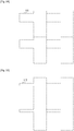
- Fig. 1A is a schematic view of a cross section of a pixel of a solid-state image pickup device according to an embodiment of the present invention.
- Reference numeral 101 denotes a photoelectric conversion portion.
- a photodiode configured to include a P-type semiconductor region and an N-type semiconductor region is used, for example.
- Reference numeral 102 denotes a charge holding portion.
- the charge holding portion 102 is configured to include an N-type semiconductor region capable of holding charges generated by the photoelectric conversion portion 101.
- Reference numeral 103 denotes a transfer portion.
- the transfer portion 103 transfers charges held by the charge holding portion 102 to a sense node.
- Reference numeral 104 denotes the sense node.
- the sense node 104 is configured to include a floating diffusion (FD) that is electrically connected to the gate of a pixel amplification metal oxide semiconductor (MOS) transistor, for example.
- the FD may be electrically connected to a vertical signal line (not illustrated), instead of being electrically connected to the gate of the pixel amplification MOS transistor.
- the photoelectric conversion portion 101, the charge holding portion 102, the transfer portion 103, and the sense node 104 are arranged on one of principal surfaces of an N-type substrate 116.
- a pixel structure is disposed on a surface of the N-type substrate 116 that is formed through epitaxial growth.
- the pixel structure may be disposed on a surface of a P-type substrate or a P-type well.
- the effect of increasing the sensitivity using the N-type substrate 116 becomes particularly significant.
- Reference numerals 105 and 106 denote N-type semiconductor regions.
- the N-type semiconductor region 105 is disposed in the N-type semiconductor region 106 and has an N-type impurity concentration higher than that of the N-type semiconductor region 106.
- the N-type semiconductor region 105 forms a PN junction together with a P-type semiconductor region 108.
- the N-type semiconductor region 106 forms a PN junction together with a P-type buried layer 107, which is disposed under the N-type semiconductor region 106.
- the P-type semiconductor region 108 is a high-concentration P-type semiconductor region. Providing the P-type semiconductor region 108 enables reduction of a dark current that is generated on a surface of semiconductor.
- the foregoing photoelectric conversion portion 101 is constituted by the N-type semiconductor regions 105 and 106, the P-type buried layer 107, and the P-type semiconductor region 108.
- Reference numeral 110 denotes an N-type semiconductor region.
- the N-type semiconductor region 110 functions as a first semiconductor region that holds charges in a portion different from the photoelectric conversion portion 101.
- Reference numeral 112 denotes a control electrode.
- the foregoing charge holding portion 102 is configured to include the N-type semiconductor region 110 and the control electrode 112.
- the charge holding portion 102 includes the control electrode 112, which is disposed above the N-type semiconductor region 110 via an insulating film 109.
- the control electrode 112 controls the potential on a semiconductor surface side of the N-type semiconductor region 110.
- a negative voltage may be applied to the control electrode 112 so as to suppress an influence of a dark current generated in the charge holding portion 102.
- the control electrode 112 may also have a function of controlling a potential between the photoelectric conversion portion 101 and the charge holding portion 102.
- a distinct electrode from the control electrode 112 may be disposed for controlling the potential between the photoelectric conversion portion 101 and the charge holding portion 102.
- An embodiment of the present invention can be applied to a configuration that does not include the control electrode 112.
- the N-type semiconductor region 110 may be selectively connected to the power source via a contact plug and a switch.
- Reference numeral 113 denotes a transfer gate electrode.
- a voltage supplied to the transfer gate electrode 113 forms a transfer path of the charge holding portion 102 in a region adjacent to the N-type semiconductor region 110.
- a pixel structure is formed on the N-type substrate 116, and thus the conductivity type of the transfer path is N-type. P-type channel doping may be performed in the region provided with the transfer path.
- the transfer gate electrode 113 is disposed so that the transfer path is formed at a position where signal charges can be transferred from the charge holding portion 102 to the sense node 104 described below.
- the transfer gate electrode 113 switches between a state where the transfer path is formed and a state where the transfer path is not formed in accordance with a voltage supplied thereto, so as to control the electrical connection between the charge holding portion 102 and the sense node 104.
- An FD 114 is an N-type semiconductor region.
- the FD 114 functions as a sense node.
- the sense node may be a semiconductor region from which a signal is output in accordance with the amount of charges accumulated therein.
- Reference numeral 115 denotes a light shielding member.
- the light shielding member 115 reduces incident light to the charge holding portion 102, the transfer portion 103, and the sense node 104, or completely blocks incident light thereto.
- Reference numeral 111 denotes a P-type semiconductor region.
- the P-type semiconductor region 111 is disposed under the N-type semiconductor region 110 and forms a potential for reducing inflow of charges from a deep portion of the substrate to the N-type semiconductor region 110.
- the P-type semiconductor region 111 is referred to as a beneath-holding-portion isolation layer for convenience.
- the beneath-holding-portion isolation layer 111 extends in the charge holding portion 102, the transfer portion 103, and the FD.
- the configuration is not limited thereto, and the beneath-holding-portion isolation layer 111 may be disposed under at least part of the N-type semiconductor region 110.
- a P-type semiconductor region 117 functioning as a pixel isolation layer is disposed under the beneath-holding-portion isolation layer 111.
- the upper end of the pixel isolation layer 117 is disposed such that the pixel isolation layer 117 and the beneath-holding-portion isolation layer 111 are in electrical conduction.
- the lower end of the pixel isolation layer 117 is at the depth where the PN junction interface between the N-type semiconductor region 106 constituting part of the photoelectric conversion portion 101 and the P-type buried layer 107 is disposed.
- the pixel isolation layer 117 functions as a potential barrier for signal charges generated in the N-type semiconductor region 106, thereby suppressing inflow of generated signal charges into an adjacent pixel.
- the end portion in the horizontal direction with respect to the substrate surface of the pixel isolation layer 117 is offset from the photoelectric conversion portion side in the same pixel, with the end portion on the photoelectric conversion portion side of the beneath-holding-portion isolation layer 111 being a reference.
- the N-type semiconductor region 106 constituting part of the photoelectric conversion portion 101 is disposed in the portion where the pixel isolation layer 117 is not disposed due to its offset end portion.
- the N-type semiconductor region 106 constituting the photoelectric conversion portion 101 is disposed under at least part of the N-type semiconductor region 110, with the beneath-holding-portion isolation layer 111 therebetween. Accordingly, the beneath-holding-portion isolation layer 111 forms a potential barrier with respect to signal charges, so that inflow of signal charges generated in a deep portion of the charge holding portion 102 into the N-type semiconductor region 110 can be suppressed.
- Figs. 1B and 1C illustrate impurity concentration distributions along a depth direction in the IB-IB cross section and the IC-IC cross section illustrated in Fig. 1A , respectively.
- the IB-IB cross section is a cross section of a portion close to the photoelectric conversion portion 101 of the N-type semiconductor region 110
- the IC-IC cross section is a cross section of a portion far from the photoelectric conversion portion 101 of the N-type semiconductor region 110.
- the impurity concentration peak of the N-type semiconductor region 110 is formed at the shallowest position with respect to the surface of the semiconductor substrate.
- the impurity concentration peak of the beneath-holding-portion isolation layer 111 exists under the impurity concentration peak of the N-type semiconductor region 110.
- the N-type semiconductor region 106 is disposed under the beneath-holding-portion isolation layer 111.
- the impurity concentration peak of the N-type semiconductor region 110 is formed at the shallowest position, and the beneath-holding-portion isolation layer 111 and the pixel isolation layer 117 are disposed thereunder with a uniform impurity concentration distribution. That is, Figs.
- FIGS. 1B and 1C illustrate that the end portion on the photoelectric conversion portion side of the pixel isolation layer 117 is offset toward the FD side, with the end portion on the photoelectric conversion portion side of the N-type semiconductor region 110 being a reference. Also, Figs. 1B and 1C illustrate that the N-type semiconductor region 106 constituting the photoelectric conversion portion 101 is disposed under at least part of the N-type semiconductor region 110 via the beneath-holding-portion isolation layer 111.
- the lower end of the pixel isolation layer 117 is at the depth where the PN junction interface between the N-type semiconductor region 106 and the P-type buried layer 107 is disposed.
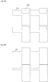
- Fig. 2 is a top view of a pixel region according to this embodiment.
- Fig. 2 illustrates four pixels, but more pixels may be provided.
- a schematic view of the IA-IA cross section in Fig. 2 is illustrated in Fig. 1A .
- the parts having the same function as in Fig. 1A are denoted by the same reference numerals, and a detailed description thereof will be omitted.
- Reference numeral 201 denotes an active region. In the active region 201, the photoelectric conversion portion 101, the N-type semiconductor region 110, the beneath-holding-portion isolation layer 111, the transfer path, and the FD 114 are disposed.
- Reference numeral 202 denotes an element isolation region. A field oxide film is used for isolation of elements, for example. Alternatively, diffusion isolation using PN junction may be used.
- Reference numeral 203 denotes an in-pixel functional element region. In the in-pixel functional element region 203, functional elements such as a pixel amplification MOS transistor and a reset MOS transistor are disposed.
- Reference numeral 204 denotes a charge discharging gate electrode that is provided if necessary.
- Reference numeral 205 denotes a contact plug connected to the FD, and an opening 206 through which the contact plug 205 is disposed is provided in the light shielding member 115.
- the beneath-holding-portion isolation layer 111 is disposed over the entire region of the N-type semiconductor region 110 and the element isolation region 202.
- Fig. 3A illustrates a top view of a pixel region, illustrating only the beneath-holding-portion isolation layer 111.
- the beneath-holding-portion isolation layer 111 is indicated by a chain line.
- the pixel isolation layer 117 is disposed under the beneath-holding-portion isolation layer 111.
- the end portion on the photoelectric conversion portion side of the pixel isolation layer 117 is offset with respect to the end portion on the photoelectric conversion portion side of the N-type semiconductor region 110.
- Fig. 3B illustrates a top view of a pixel region, illustrating only the pixel isolation layer 117.
- the pixel isolation layer 117 is indicated by a chain line.
- the width of the pixel isolation layer 117 is smaller than the width of the beneath-holding-portion isolation layer 111. That is, the pixel isolation layer 117 is offset from both the photoelectric conversion portion 101 of the pixel and the photoelectric conversion portion 101 of the adjacent pixel.
- the solid-state image pickup device has a pixel structure in which a photoelectric conversion portion, a charge holding portion, and an FD are arranged in an L shape.
- the charge holding portion is disposed between the photoelectric conversion portion of the pixel and the photoelectric conversion portion of the adjacent pixel.
- Fig. 1A illustrates a cross section in which the end portion of the pixel isolation layer 117 is offset with respect to the photoelectric conversion portion 101 of the pixel.
- the end portion of the pixel isolation layer 117 may be offset with respect to the photoelectric conversion portion 101 of the adjacent pixel as well.
- the end portion of the pixel isolation layer 117 may not be offset with respect to the photoelectric conversion portion 101 of the pixel, and may be offset with respect to the photoelectric conversion portion 101 of the adjacent pixel.
- the end portion of the pixel isolation layer 117 may be offset with respect to at least one of photoelectric conversion portions adjacent to the charge holding portion of the pixel.
- the pixel isolation layer 117 under the beneath-holding-portion isolation layer 111 is offset from the photoelectric conversion portion 101, and the N-type semiconductor region 106 is disposed in the offset region.
- the beneath-holding-portion isolation layer 111 serves as a potential barrier with respect to signal charges, so that inflow of charges generated in a lower portion of the charge holding portion 102 into the N-type semiconductor region 110 can be suppressed.
- the pixel isolation layer 117 suppresses inflow of charges into a different pixel.
- the N-type semiconductor region 106 that is disposed in the region where the pixel isolation layer 117 is offset in a lower portion of the holding portion is part of the photoelectric conversion portion 101, and thus more charges are collected in the photoelectric conversion portion 101.
- Fig. 4A is a schematic view of a cross section of a pixel of a solid-state image pickup device according to a second embodiment of the present invention.
- the parts having the same function as those in the first embodiment are denoted by the same reference numerals, and a detailed description thereof will be omitted.
- the pixel isolation layer is constituted by P-type semiconductor regions 117a, 117b, and 117c that are disposed at different depths.
- the pixel isolation layer is constituted by the three semiconductor regions.
- the number of semiconductor regions is not limited to three, and the pixel isolation layer may be constituted by a plurality of semiconductor regions at different depths.
- the individual semiconductor regions may be formed through ion implantation steps using different acceleration energies.
- Figs. 4B and 4C illustrate impurity concentration distributions along a depth direction in the IVB-IVB cross section and the IVC-IVC cross section illustrate in Fig. 4A , respectively.
- the N-type semiconductor region 106 is disposed under at least part of the N-type semiconductor region 110 via the beneath-holding-portion isolation layer 111.
- the impurity concentration peak of the N-type semiconductor region 110 is at a position that is the closest to the surface.
- the impurity concentration peak of the beneath-holding-portion isolation layer 111 is at a position that is the second closest to the surface.
- the impurity distribution is nonuniform under the impurity concentration peak of the beneath-holding-portion isolation layer 111. Instead, the impurity concentration peaks of the three P-type semiconductor regions 117a, 117b, and 117c can be seen.
- the impurity concentration peak of the P-type buried layer 107 is at the deepest position.
- the P-type buried layer 107 is disposed at as deep position as possible with respect to the surface of the substrate provided with pixels. Accordingly, charges generated in a deep portion of the substrate are not discharged to the substrate side, and are easily collected as signal charges in the photoelectric conversion portion 101.
- the P-type buried layer 107 is disposed at a deep position of the substrate, it is difficult to constitute the pixel isolation layer by a single layer of semiconductor region. In contrast, by constituting the pixel isolation layer by a plurality of semiconductor regions disposed at different depths, the pixel isolation layer can be formed at a deeper position.
- the impurity concentration of the beneath-holding-portion isolation layer 111 is higher than the impurity concentration of the P-type semiconductor region 117a, which is the closest to the substrate surface among the P-type semiconductor regions 117a to 117c.
- the impurity concentration peak of the beneath-holding-portion isolation layer 111 is higher than the impurity concentration peak of the P-type semiconductor region 117a.
- the pixel isolation layer is constituted by a plurality of semiconductor regions having different impurity concentrations.
- the plurality of semiconductor regions may have impurity concentrations equal to each other.
- the impurity concentrations of the plurality of semiconductor regions constituting the pixel isolation layer may be equal to the impurity concentration of the beneath-holding-portion isolation layer 111.
- the pixel isolation layer is constituted by a plurality of semiconductor regions that are disposed at different depths. Accordingly, the pixel isolation layer can be easily disposed at a deep position. Therefore, according to this embodiment, it is possible to further increase the sensitivity and suppress inflow of charges into an adjacent pixel, in addition to obtain the effect in the first embodiment.
- the impurity concentration of the beneath-holding-portion isolation layer 111 is higher than the impurity concentration of the P-type semiconductor region 117a which is the closest to the substrate surface among the P-type semiconductor regions 117a to 117c. Accordingly, inflow of charges generated in the pixel isolation layer into the N-type semiconductor region 110 is reduced. As described above, according to this embodiment, it is possible to further suppress inflow of charges into the charge holding portion 102, in addition to obtain the effect in the first embodiment.
- Fig. 5 is a schematic view of a cross section of a pixel of a solid-state image pickup device according to a third embodiment of the present invention.
- the parts having the same function as those in the first and second embodiments are denoted by the same reference numerals, and a detailed description thereof will be omitted.
- a difference between this embodiment and the first and second embodiments is that, as illustrated in Fig. 5 , at the depth where the impurity concentration peak of the beneath-holding-portion isolation layer 111 exists, the impurity concentration of the beneath-holding-portion isolation layer 111 is higher than the impurity concentration of the region under the FD 114 at the same depth.
- the beneath-holding-portion isolation layer 111 which is a high-concentration P-type semiconductor region, does not exist, or the impurity concentration thereof is low.
- Figs. 6A, 6B, and 6C illustrate impurity concentration distributions along a depth direction in the VIA-VIA cross section, the VIB-VIB cross section, and the VIC-VIC cross section illustrate in Fig. 5 , respectively.
- the impurity concentration distributions in the VIA-VIA cross section and the VIB-VIB cross section are the same as those in the second embodiment.
- the impurity concentration at the same depth as the impurity concentration peak of the beneath-holding-portion isolation layer 111 is lower than the impurity concentration of the beneath-holding-portion isolation layer 111.
- the N-type semiconductor region 110 does not extend.
- the beneath-holding-portion isolation layer 111 does not exist in the transfer portion 103 where the N-type semiconductor region 110 does not exist, neither under the FD 114.
- Fig. 7 is a top view of a pixel region according to this embodiment.
- Fig. 7 illustrates only four pixels, but the solid-state image pickup device according to this embodiment may include more pixels.
- a schematic view of the V-V cross section in Fig. 7 is illustrated in Fig. 5 .
- the parts having the same function as in Fig. 5 are denoted by the same reference numerals, and a detailed description thereof will be omitted.
- a region 401 indicated by a chain line in Fig. 7 represents a region where the beneath-holding-portion isolation layer 111 does not exist.
- Fig. 8A is a top view illustrating only the beneath-holding-portion isolation layer 111.
- the beneath-holding-portion isolation layer 111 is disposed over the entire N-type semiconductor region 110.
- the beneath-holding-portion isolation layer 111 does not exist in the transfer portion 103 and under the FD 114.
- the region 401 indicated by a chain line represents a region where the beneath-holding-portion isolation layer 111 does not exist.
- Fig. 8B is a top view illustrating only the pixel isolation layer 117.
- the planar shape of the pixel isolation layer 117 is the same as that in the first embodiment or the second embodiment.
- the beneath-holding-portion isolation layer 111 does not exist in the transfer portion 103 and under the FD 114. Accordingly, charges generated in the pixel isolation layer 117 do not flow into the N-type semiconductor region 110 or the photoelectric conversion portion 101 of an adjacent pixel, and the possibility that the charges are discharged to the FD 114 becomes high.
- the FD 114 is reset before signal charges are transferred, and thus the charges discharged to the FD 114 do not cause noise.
- Fig. 9 is an equivalent circuit diagram of a solid-state image pickup device that can be applied to all the foregoing embodiments.
- the solid-state image pickup device having this equivalent circuit can perform a global electronic shutter operation.
- Reference numeral 601 denotes a photoelectric conversion portion. A photodiode is used here.
- Reference numeral 602 denotes a charge holding portion, which holds signal charges generated by the photoelectric conversion portion 601.
- Reference numeral 603 denotes a sense node of an amplifying portion. For example, an FD and a gate electrode of an amplifying transistor that is electrically connected to the FD correspond to the sense node 603.
- Reference numeral 604 denotes a first transfer portion, which transfers charges in the charge holding portion 602 to the sense node 603 of the amplifying portion.
- Reference numeral 605 denotes a second transfer portion that is provided if necessary. The second transfer portion 605 transfers charges in the photoelectric conversion portion 601 to the charge holding portion 602.
- Reference numeral 608 denotes a reset portion, which supplies a reference voltage to at least an input portion of the amplifying portion. Furthermore, the reset portion 608 may supply a reference voltage to the charge holding portion 602.
- Reference numeral 607 denotes a selecting portion that is provided if necessary. The selecting portion 607 selectively outputs signals of respective pixel rows to a signal line.
- Reference numeral 606 denotes an amplifying portion. The amplifying portion 606 constitutes a source follower circuit together with a constant current source provided to the signal line.
- Reference numeral 609 denotes a charge output control portion, which controls the electrical connection between the photoelectric conversion portion 601 and a power supply line functioning as an overflow drain (hereinafter OFD).
- OFD overflow drain
- Reference symbol RES denotes a wire for supplying a drive pulse to the reset portion 608.
- Reference symbol TX1 denotes a wire for supplying a drive pulse to the first transfer portion 604.
- Reference symbol TX2 denotes a wire for supplying a drive pulse to the second transfer portion 605. This wire can also serve as a wire for supplying a control pulse of the control electrode in the charge holding portion 602.
- Reference symbol SEL denotes a wire for supplying a drive pulse to the selecting portion 607.
- the equivalent circuit is not limited thereto, and part of the configuration may be shared by a plurality of pixels. Also, the equivalent circuit is applicable to a configuration in which control wiring of individual elements is fixed to a constant voltage and in which control of conduction is not performed.
- the second transfer portion 605 may have a buried channel MOS transistor configuration so that charges generated by the photoelectric conversion portion 601 immediately flow into the charge holding portion 602.
- a potential barrier is partially low at a position deeper than a surface even in a non-conduction state.
- the charge transfer portion can be brought into a state where a certain voltage is supplied without performing active control. That is, a fixed potential barrier may be provided instead of a function as a transfer portion.
- the potential of the charge path between the photoelectric conversion portion 601 and the charge holding portion 602 is lower than the potential of the charge path between the photoelectric conversion portion 601 and the OFD region.
- the potential means the potential for signal charges.
- charges moved from the photoelectric conversion portion 601 to the charge holding portion 602 in one exposure period are held in the charge holding portion 602 and are used as an image signal. That is, after one exposure period in the photoelectric conversion portion 601 starts, a signal is read from the pixel without through a reset operation of the charge holding portion 602. Note that one exposure period is commonly determined in the individual photoelectric conversion portions 601 when an image of one frame is captured.
- charges can be transferred at a low voltage from the photoelectric conversion portion 601 to the charge holding portion 602, which is appropriate in terms of increasing charge transfer efficiency at a low voltage when the pixel configuration is combined with the embodiments of the present invention.
- An embodiment of the present invention can be carried out also in a solid-state image pickup device in which a charge holding portion is provided in each pixel for increasing a dynamic range and in which charges are transferred from the charge holding portion to a sense node.
Landscapes
- Engineering & Computer Science (AREA)
- Multimedia (AREA)
- Signal Processing (AREA)
- Solid State Image Pick-Up Elements (AREA)
- Transforming Light Signals Into Electric Signals (AREA)
Applications Claiming Priority (2)
| Application Number | Priority Date | Filing Date | Title |
|---|---|---|---|
| JP2009235088A JP5546198B2 (ja) | 2009-10-09 | 2009-10-09 | 固体撮像装置 |
| PCT/JP2010/005841 WO2011043035A1 (en) | 2009-10-09 | 2010-09-29 | Solid-state image pickup device |
Publications (2)
| Publication Number | Publication Date |
|---|---|
| EP2486588A1 EP2486588A1 (en) | 2012-08-15 |
| EP2486588B1 true EP2486588B1 (en) | 2018-07-18 |
Family
ID=43109811
Family Applications (1)
| Application Number | Title | Priority Date | Filing Date |
|---|---|---|---|
| EP10770882.8A Not-in-force EP2486588B1 (en) | 2009-10-09 | 2010-09-29 | Solid-state image pickup device |
Country Status (5)
| Country | Link |
|---|---|
| US (2) | US9041132B2 (OSRAM) |
| EP (1) | EP2486588B1 (OSRAM) |
| JP (1) | JP5546198B2 (OSRAM) |
| CN (1) | CN102576717B (OSRAM) |
| WO (1) | WO2011043035A1 (OSRAM) |
Families Citing this family (8)
| Publication number | Priority date | Publication date | Assignee | Title |
|---|---|---|---|---|
| JP6095258B2 (ja) | 2011-05-27 | 2017-03-15 | キヤノン株式会社 | 固体撮像装置、及び固体撮像装置を用いた撮像システム |
| US9231007B2 (en) * | 2013-08-27 | 2016-01-05 | Semiconductor Components Industries, Llc | Image sensors operable in global shutter mode and having small pixels with high well capacity |
| JP6141160B2 (ja) * | 2013-09-25 | 2017-06-07 | ソニーセミコンダクタソリューションズ株式会社 | 固体撮像素子およびその動作方法、並びに電子機器およびその動作方法 |
| JP6308864B2 (ja) * | 2014-05-15 | 2018-04-11 | キヤノン株式会社 | 撮像装置 |
| JP2016187018A (ja) * | 2015-03-27 | 2016-10-27 | キヤノン株式会社 | 光電変換装置およびカメラ |
| US10396108B2 (en) | 2015-10-27 | 2019-08-27 | Sony Semiconductor Solutions Corporation | Solid-state imaging element, solid-state imaging element manufacturing method, and electronic apparatus |
| JP6407227B2 (ja) * | 2016-10-05 | 2018-10-17 | キヤノン株式会社 | 固体撮像装置、及び固体撮像装置を用いた撮像システム |
| JP6661723B2 (ja) * | 2018-09-19 | 2020-03-11 | キヤノン株式会社 | 固体撮像装置、及び固体撮像装置を用いた撮像システム |
Citations (1)
| Publication number | Priority date | Publication date | Assignee | Title |
|---|---|---|---|---|
| EP2486590B1 (en) * | 2009-10-09 | 2013-12-11 | Canon Kabushiki Kaisha | Solid-state image pickup device |
Family Cites Families (13)
| Publication number | Priority date | Publication date | Assignee | Title |
|---|---|---|---|---|
| JP3702854B2 (ja) * | 2002-03-06 | 2005-10-05 | ソニー株式会社 | 固体撮像素子 |
| TWI353979B (en) | 2002-04-10 | 2011-12-11 | Nippon Zoki Pharmaceutical Co | Novel crystal form of 5-hydroxy-1-methylhydantoin |
| WO2003096421A1 (en) | 2002-05-14 | 2003-11-20 | Sony Corporation | Semiconductor device and its manufacturing method, and electronic device |
| WO2004017411A1 (ja) | 2002-08-12 | 2004-02-26 | Sony Corporation | 固体撮像素子及びその製造方法 |
| JP2004165462A (ja) | 2002-11-14 | 2004-06-10 | Sony Corp | 固体撮像素子及びその製造方法 |
| US7153719B2 (en) * | 2004-08-24 | 2006-12-26 | Micron Technology, Inc. | Method of fabricating a storage gate pixel design |
| JP4416668B2 (ja) | 2005-01-14 | 2010-02-17 | キヤノン株式会社 | 固体撮像装置、その制御方法及びカメラ |
| JP4273124B2 (ja) | 2005-02-04 | 2009-06-03 | キヤノン株式会社 | 撮像装置及び撮像システム |
| JP4785433B2 (ja) | 2005-06-10 | 2011-10-05 | キヤノン株式会社 | 固体撮像装置 |
| US7605440B2 (en) * | 2006-04-07 | 2009-10-20 | Aptina Imaging Corporation | Pixel cell isolation of charge storage and floating diffusion regions using doped wells |
| JP2008004692A (ja) * | 2006-06-21 | 2008-01-10 | Nikon Corp | 固体撮像装置 |
| JP2009038167A (ja) | 2007-08-01 | 2009-02-19 | Victor Co Of Japan Ltd | 固体撮像装置及びその製造方法 |
| JP5213501B2 (ja) | 2008-04-09 | 2013-06-19 | キヤノン株式会社 | 固体撮像装置 |
-
2009
- 2009-10-09 JP JP2009235088A patent/JP5546198B2/ja active Active
-
2010
- 2010-09-29 US US13/500,043 patent/US9041132B2/en not_active Expired - Fee Related
- 2010-09-29 CN CN201080044580.4A patent/CN102576717B/zh active Active
- 2010-09-29 EP EP10770882.8A patent/EP2486588B1/en not_active Not-in-force
- 2010-09-29 WO PCT/JP2010/005841 patent/WO2011043035A1/en not_active Ceased
-
2015
- 2015-04-22 US US14/693,692 patent/US9502465B2/en active Active
Patent Citations (1)
| Publication number | Priority date | Publication date | Assignee | Title |
|---|---|---|---|---|
| EP2486590B1 (en) * | 2009-10-09 | 2013-12-11 | Canon Kabushiki Kaisha | Solid-state image pickup device |
Also Published As
| Publication number | Publication date |
|---|---|
| US9041132B2 (en) | 2015-05-26 |
| EP2486588A1 (en) | 2012-08-15 |
| US9502465B2 (en) | 2016-11-22 |
| WO2011043035A1 (en) | 2011-04-14 |
| JP5546198B2 (ja) | 2014-07-09 |
| CN102576717A (zh) | 2012-07-11 |
| US20150228692A1 (en) | 2015-08-13 |
| US20120199933A1 (en) | 2012-08-09 |
| CN102576717B (zh) | 2015-04-01 |
| JP2011082426A (ja) | 2011-04-21 |
Similar Documents
| Publication | Publication Date | Title |
|---|---|---|
| US9502465B2 (en) | Solid-state image pickup device | |
| EP2486590B1 (en) | Solid-state image pickup device | |
| US8896734B2 (en) | Solid-state image sensor, method of manufacturing the same, and camera | |
| US8710613B2 (en) | Pickup device and method for manufacturing the same | |
| JP2009253149A (ja) | 光電変換装置及びそれを用いた撮像システム | |
| US8823125B2 (en) | Solid-state image pickup device and method for manufacturing the same | |
| JP2013251559A (ja) | 光電変換装置及びそれを用いた撮像システム | |
| HK1171571B (en) | Solid-state image pickup device and method for manufacturing same | |
| JP2015111728A (ja) | 光電変換装置及びそれを用いた撮像システム |
Legal Events
| Date | Code | Title | Description |
|---|---|---|---|
| PUAI | Public reference made under article 153(3) epc to a published international application that has entered the european phase |
Free format text: ORIGINAL CODE: 0009012 |
|
| 17P | Request for examination filed |
Effective date: 20120509 |
|
| AK | Designated contracting states |
Kind code of ref document: A1 Designated state(s): AL AT BE BG CH CY CZ DE DK EE ES FI FR GB GR HR HU IE IS IT LI LT LU LV MC MK MT NL NO PL PT RO SE SI SK SM TR |
|
| DAX | Request for extension of the european patent (deleted) | ||
| 17Q | First examination report despatched |
Effective date: 20130402 |
|
| GRAP | Despatch of communication of intention to grant a patent |
Free format text: ORIGINAL CODE: EPIDOSNIGR1 |
|
| RAP1 | Party data changed (applicant data changed or rights of an application transferred) |
Owner name: CANON KABUSHIKI KAISHA |
|
| INTG | Intention to grant announced |
Effective date: 20180213 |
|
| GRAS | Grant fee paid |
Free format text: ORIGINAL CODE: EPIDOSNIGR3 |
|
| GRAA | (expected) grant |
Free format text: ORIGINAL CODE: 0009210 |
|
| AK | Designated contracting states |
Kind code of ref document: B1 Designated state(s): AL AT BE BG CH CY CZ DE DK EE ES FI FR GB GR HR HU IE IS IT LI LT LU LV MC MK MT NL NO PL PT RO SE SI SK SM TR |
|
| REG | Reference to a national code |
Ref country code: GB Ref legal event code: FG4D |
|
| REG | Reference to a national code |
Ref country code: CH Ref legal event code: EP |
|
| REG | Reference to a national code |
Ref country code: IE Ref legal event code: FG4D |
|
| REG | Reference to a national code |
Ref country code: DE Ref legal event code: R096 Ref document number: 602010052024 Country of ref document: DE |
|
| REG | Reference to a national code |
Ref country code: AT Ref legal event code: REF Ref document number: 1020268 Country of ref document: AT Kind code of ref document: T Effective date: 20180815 |
|
| REG | Reference to a national code |
Ref country code: NL Ref legal event code: MP Effective date: 20180718 |
|
| REG | Reference to a national code |
Ref country code: LT Ref legal event code: MG4D |
|
| REG | Reference to a national code |
Ref country code: AT Ref legal event code: MK05 Ref document number: 1020268 Country of ref document: AT Kind code of ref document: T Effective date: 20180718 |
|
| PG25 | Lapsed in a contracting state [announced via postgrant information from national office to epo] |
Ref country code: NL Free format text: LAPSE BECAUSE OF FAILURE TO SUBMIT A TRANSLATION OF THE DESCRIPTION OR TO PAY THE FEE WITHIN THE PRESCRIBED TIME-LIMIT Effective date: 20180718 |
|
| PG25 | Lapsed in a contracting state [announced via postgrant information from national office to epo] |
Ref country code: FI Free format text: LAPSE BECAUSE OF FAILURE TO SUBMIT A TRANSLATION OF THE DESCRIPTION OR TO PAY THE FEE WITHIN THE PRESCRIBED TIME-LIMIT Effective date: 20180718 Ref country code: LT Free format text: LAPSE BECAUSE OF FAILURE TO SUBMIT A TRANSLATION OF THE DESCRIPTION OR TO PAY THE FEE WITHIN THE PRESCRIBED TIME-LIMIT Effective date: 20180718 Ref country code: BG Free format text: LAPSE BECAUSE OF FAILURE TO SUBMIT A TRANSLATION OF THE DESCRIPTION OR TO PAY THE FEE WITHIN THE PRESCRIBED TIME-LIMIT Effective date: 20181018 Ref country code: NO Free format text: LAPSE BECAUSE OF FAILURE TO SUBMIT A TRANSLATION OF THE DESCRIPTION OR TO PAY THE FEE WITHIN THE PRESCRIBED TIME-LIMIT Effective date: 20181018 Ref country code: GR Free format text: LAPSE BECAUSE OF FAILURE TO SUBMIT A TRANSLATION OF THE DESCRIPTION OR TO PAY THE FEE WITHIN THE PRESCRIBED TIME-LIMIT Effective date: 20181019 Ref country code: AT Free format text: LAPSE BECAUSE OF FAILURE TO SUBMIT A TRANSLATION OF THE DESCRIPTION OR TO PAY THE FEE WITHIN THE PRESCRIBED TIME-LIMIT Effective date: 20180718 Ref country code: IS Free format text: LAPSE BECAUSE OF FAILURE TO SUBMIT A TRANSLATION OF THE DESCRIPTION OR TO PAY THE FEE WITHIN THE PRESCRIBED TIME-LIMIT Effective date: 20181118 Ref country code: PL Free format text: LAPSE BECAUSE OF FAILURE TO SUBMIT A TRANSLATION OF THE DESCRIPTION OR TO PAY THE FEE WITHIN THE PRESCRIBED TIME-LIMIT Effective date: 20180718 Ref country code: SE Free format text: LAPSE BECAUSE OF FAILURE TO SUBMIT A TRANSLATION OF THE DESCRIPTION OR TO PAY THE FEE WITHIN THE PRESCRIBED TIME-LIMIT Effective date: 20180718 |
|
| PG25 | Lapsed in a contracting state [announced via postgrant information from national office to epo] |
Ref country code: LV Free format text: LAPSE BECAUSE OF FAILURE TO SUBMIT A TRANSLATION OF THE DESCRIPTION OR TO PAY THE FEE WITHIN THE PRESCRIBED TIME-LIMIT Effective date: 20180718 Ref country code: AL Free format text: LAPSE BECAUSE OF FAILURE TO SUBMIT A TRANSLATION OF THE DESCRIPTION OR TO PAY THE FEE WITHIN THE PRESCRIBED TIME-LIMIT Effective date: 20180718 Ref country code: HR Free format text: LAPSE BECAUSE OF FAILURE TO SUBMIT A TRANSLATION OF THE DESCRIPTION OR TO PAY THE FEE WITHIN THE PRESCRIBED TIME-LIMIT Effective date: 20180718 |
|
| REG | Reference to a national code |
Ref country code: DE Ref legal event code: R097 Ref document number: 602010052024 Country of ref document: DE |
|
| PG25 | Lapsed in a contracting state [announced via postgrant information from national office to epo] |
Ref country code: MC Free format text: LAPSE BECAUSE OF FAILURE TO SUBMIT A TRANSLATION OF THE DESCRIPTION OR TO PAY THE FEE WITHIN THE PRESCRIBED TIME-LIMIT Effective date: 20180718 Ref country code: IT Free format text: LAPSE BECAUSE OF FAILURE TO SUBMIT A TRANSLATION OF THE DESCRIPTION OR TO PAY THE FEE WITHIN THE PRESCRIBED TIME-LIMIT Effective date: 20180718 Ref country code: EE Free format text: LAPSE BECAUSE OF FAILURE TO SUBMIT A TRANSLATION OF THE DESCRIPTION OR TO PAY THE FEE WITHIN THE PRESCRIBED TIME-LIMIT Effective date: 20180718 Ref country code: RO Free format text: LAPSE BECAUSE OF FAILURE TO SUBMIT A TRANSLATION OF THE DESCRIPTION OR TO PAY THE FEE WITHIN THE PRESCRIBED TIME-LIMIT Effective date: 20180718 Ref country code: ES Free format text: LAPSE BECAUSE OF FAILURE TO SUBMIT A TRANSLATION OF THE DESCRIPTION OR TO PAY THE FEE WITHIN THE PRESCRIBED TIME-LIMIT Effective date: 20180718 Ref country code: CZ Free format text: LAPSE BECAUSE OF FAILURE TO SUBMIT A TRANSLATION OF THE DESCRIPTION OR TO PAY THE FEE WITHIN THE PRESCRIBED TIME-LIMIT Effective date: 20180718 |
|
| REG | Reference to a national code |
Ref country code: CH Ref legal event code: PL |
|
| PLBE | No opposition filed within time limit |
Free format text: ORIGINAL CODE: 0009261 |
|
| STAA | Information on the status of an ep patent application or granted ep patent |
Free format text: STATUS: NO OPPOSITION FILED WITHIN TIME LIMIT |
|
| PG25 | Lapsed in a contracting state [announced via postgrant information from national office to epo] |
Ref country code: DK Free format text: LAPSE BECAUSE OF FAILURE TO SUBMIT A TRANSLATION OF THE DESCRIPTION OR TO PAY THE FEE WITHIN THE PRESCRIBED TIME-LIMIT Effective date: 20180718 Ref country code: SM Free format text: LAPSE BECAUSE OF FAILURE TO SUBMIT A TRANSLATION OF THE DESCRIPTION OR TO PAY THE FEE WITHIN THE PRESCRIBED TIME-LIMIT Effective date: 20180718 Ref country code: SK Free format text: LAPSE BECAUSE OF FAILURE TO SUBMIT A TRANSLATION OF THE DESCRIPTION OR TO PAY THE FEE WITHIN THE PRESCRIBED TIME-LIMIT Effective date: 20180718 |
|
| REG | Reference to a national code |
Ref country code: BE Ref legal event code: MM Effective date: 20180930 |
|
| 26N | No opposition filed |
Effective date: 20190423 |
|
| GBPC | Gb: european patent ceased through non-payment of renewal fee |
Effective date: 20181018 |
|
| REG | Reference to a national code |
Ref country code: IE Ref legal event code: MM4A |
|
| PG25 | Lapsed in a contracting state [announced via postgrant information from national office to epo] |
Ref country code: LU Free format text: LAPSE BECAUSE OF NON-PAYMENT OF DUE FEES Effective date: 20180929 |
|
| PG25 | Lapsed in a contracting state [announced via postgrant information from national office to epo] |
Ref country code: IE Free format text: LAPSE BECAUSE OF NON-PAYMENT OF DUE FEES Effective date: 20180929 |
|
| PG25 | Lapsed in a contracting state [announced via postgrant information from national office to epo] |
Ref country code: CH Free format text: LAPSE BECAUSE OF NON-PAYMENT OF DUE FEES Effective date: 20180930 Ref country code: FR Free format text: LAPSE BECAUSE OF NON-PAYMENT OF DUE FEES Effective date: 20180930 Ref country code: LI Free format text: LAPSE BECAUSE OF NON-PAYMENT OF DUE FEES Effective date: 20180930 Ref country code: BE Free format text: LAPSE BECAUSE OF NON-PAYMENT OF DUE FEES Effective date: 20180930 Ref country code: SI Free format text: LAPSE BECAUSE OF FAILURE TO SUBMIT A TRANSLATION OF THE DESCRIPTION OR TO PAY THE FEE WITHIN THE PRESCRIBED TIME-LIMIT Effective date: 20180718 |
|
| PG25 | Lapsed in a contracting state [announced via postgrant information from national office to epo] |
Ref country code: GB Free format text: LAPSE BECAUSE OF NON-PAYMENT OF DUE FEES Effective date: 20181018 |
|
| PG25 | Lapsed in a contracting state [announced via postgrant information from national office to epo] |
Ref country code: MT Free format text: LAPSE BECAUSE OF NON-PAYMENT OF DUE FEES Effective date: 20180929 |
|
| PGFP | Annual fee paid to national office [announced via postgrant information from national office to epo] |
Ref country code: DE Payment date: 20191129 Year of fee payment: 10 |
|
| PG25 | Lapsed in a contracting state [announced via postgrant information from national office to epo] |
Ref country code: TR Free format text: LAPSE BECAUSE OF FAILURE TO SUBMIT A TRANSLATION OF THE DESCRIPTION OR TO PAY THE FEE WITHIN THE PRESCRIBED TIME-LIMIT Effective date: 20180718 |
|
| PG25 | Lapsed in a contracting state [announced via postgrant information from national office to epo] |
Ref country code: PT Free format text: LAPSE BECAUSE OF FAILURE TO SUBMIT A TRANSLATION OF THE DESCRIPTION OR TO PAY THE FEE WITHIN THE PRESCRIBED TIME-LIMIT Effective date: 20180718 Ref country code: HU Free format text: LAPSE BECAUSE OF FAILURE TO SUBMIT A TRANSLATION OF THE DESCRIPTION OR TO PAY THE FEE WITHIN THE PRESCRIBED TIME-LIMIT; INVALID AB INITIO Effective date: 20100929 |
|
| PG25 | Lapsed in a contracting state [announced via postgrant information from national office to epo] |
Ref country code: MK Free format text: LAPSE BECAUSE OF NON-PAYMENT OF DUE FEES Effective date: 20180718 Ref country code: CY Free format text: LAPSE BECAUSE OF FAILURE TO SUBMIT A TRANSLATION OF THE DESCRIPTION OR TO PAY THE FEE WITHIN THE PRESCRIBED TIME-LIMIT Effective date: 20180718 |
|
| REG | Reference to a national code |
Ref country code: DE Ref legal event code: R119 Ref document number: 602010052024 Country of ref document: DE |
|
| PG25 | Lapsed in a contracting state [announced via postgrant information from national office to epo] |
Ref country code: DE Free format text: LAPSE BECAUSE OF NON-PAYMENT OF DUE FEES Effective date: 20210401 |