EP2485071B1 - Anorganischer optischer filter, optisches element und lichtquelle - Google Patents
Anorganischer optischer filter, optisches element und lichtquelle Download PDFInfo
- Publication number
- EP2485071B1 EP2485071B1 EP10820351.4A EP10820351A EP2485071B1 EP 2485071 B1 EP2485071 B1 EP 2485071B1 EP 10820351 A EP10820351 A EP 10820351A EP 2485071 B1 EP2485071 B1 EP 2485071B1
- Authority
- EP
- European Patent Office
- Prior art keywords
- wavelength
- single crystal
- range
- light
- container
- Prior art date
- Legal status (The legal status is an assumption and is not a legal conclusion. Google has not performed a legal analysis and makes no representation as to the accuracy of the status listed.)
- Not-in-force
Links
- 230000003287 optical effect Effects 0.000 title claims description 82
- 239000013078 crystal Substances 0.000 claims description 143
- 238000006243 chemical reaction Methods 0.000 claims description 61
- 238000002834 transmittance Methods 0.000 claims description 36
- KRHYYFGTRYWZRS-UHFFFAOYSA-M Fluoride anion Chemical compound [F-] KRHYYFGTRYWZRS-UHFFFAOYSA-M 0.000 claims description 17
- 238000001228 spectrum Methods 0.000 claims description 17
- 239000007787 solid Substances 0.000 claims description 14
- 229910017557 NdF3 Inorganic materials 0.000 claims 4
- XRADHEAKQRNYQQ-UHFFFAOYSA-K trifluoroneodymium Chemical compound F[Nd](F)F XRADHEAKQRNYQQ-UHFFFAOYSA-K 0.000 description 30
- 239000000203 mixture Substances 0.000 description 23
- 239000000463 material Substances 0.000 description 13
- 239000002516 radical scavenger Substances 0.000 description 13
- RTAQQCXQSZGOHL-UHFFFAOYSA-N Titanium Chemical compound [Ti] RTAQQCXQSZGOHL-UHFFFAOYSA-N 0.000 description 11
- 239000010936 titanium Substances 0.000 description 11
- 229910052719 titanium Inorganic materials 0.000 description 11
- YCKRFDGAMUMZLT-UHFFFAOYSA-N Fluorine atom Chemical compound [F] YCKRFDGAMUMZLT-UHFFFAOYSA-N 0.000 description 10
- 229910052731 fluorine Inorganic materials 0.000 description 10
- 239000011737 fluorine Substances 0.000 description 10
- 150000001875 compounds Chemical class 0.000 description 9
- 239000007789 gas Substances 0.000 description 9
- 239000000843 powder Substances 0.000 description 9
- 239000007788 liquid Substances 0.000 description 7
- 238000000034 method Methods 0.000 description 7
- 239000007858 starting material Substances 0.000 description 7
- 238000010586 diagram Methods 0.000 description 6
- 238000010438 heat treatment Methods 0.000 description 6
- 239000011812 mixed powder Substances 0.000 description 6
- 239000011261 inert gas Substances 0.000 description 5
- 229910001635 magnesium fluoride Inorganic materials 0.000 description 5
- XKRFYHLGVUSROY-UHFFFAOYSA-N Argon Chemical compound [Ar] XKRFYHLGVUSROY-UHFFFAOYSA-N 0.000 description 4
- 230000000903 blocking effect Effects 0.000 description 4
- 238000010276 construction Methods 0.000 description 4
- 230000001747 exhibiting effect Effects 0.000 description 4
- 238000004519 manufacturing process Methods 0.000 description 4
- -1 polytetrafluoroethylene Polymers 0.000 description 4
- 229920001343 polytetrafluoroethylene Polymers 0.000 description 4
- 239000004810 polytetrafluoroethylene Substances 0.000 description 4
- BHHYHSUAOQUXJK-UHFFFAOYSA-L zinc fluoride Chemical compound F[Zn]F BHHYHSUAOQUXJK-UHFFFAOYSA-L 0.000 description 4
- OKTJSMMVPCPJKN-UHFFFAOYSA-N Carbon Chemical compound [C] OKTJSMMVPCPJKN-UHFFFAOYSA-N 0.000 description 3
- WUKWITHWXAAZEY-UHFFFAOYSA-L calcium difluoride Chemical compound [F-].[F-].[Ca+2] WUKWITHWXAAZEY-UHFFFAOYSA-L 0.000 description 3
- 229910001634 calcium fluoride Inorganic materials 0.000 description 3
- 229910052799 carbon Inorganic materials 0.000 description 3
- 230000000052 comparative effect Effects 0.000 description 3
- 230000000694 effects Effects 0.000 description 3
- 239000001307 helium Substances 0.000 description 3
- 229910052734 helium Inorganic materials 0.000 description 3
- SWQJXJOGLNCZEY-UHFFFAOYSA-N helium atom Chemical compound [He] SWQJXJOGLNCZEY-UHFFFAOYSA-N 0.000 description 3
- 238000002844 melting Methods 0.000 description 3
- 230000008018 melting Effects 0.000 description 3
- 230000000737 periodic effect Effects 0.000 description 3
- 230000010287 polarization Effects 0.000 description 3
- IJGRMHOSHXDMSA-UHFFFAOYSA-N Atomic nitrogen Chemical compound N#N IJGRMHOSHXDMSA-UHFFFAOYSA-N 0.000 description 2
- 229910005270 GaF3 Inorganic materials 0.000 description 2
- 229910004504 HfF4 Inorganic materials 0.000 description 2
- UFHFLCQGNIYNRP-UHFFFAOYSA-N Hydrogen Chemical compound [H][H] UFHFLCQGNIYNRP-UHFFFAOYSA-N 0.000 description 2
- 229910010348 TiF3 Inorganic materials 0.000 description 2
- 229910007998 ZrF4 Inorganic materials 0.000 description 2
- 239000000654 additive Substances 0.000 description 2
- 230000000996 additive effect Effects 0.000 description 2
- GUNJVIDCYZYFGV-UHFFFAOYSA-K antimony trifluoride Chemical compound F[Sb](F)F GUNJVIDCYZYFGV-UHFFFAOYSA-K 0.000 description 2
- 229910052786 argon Inorganic materials 0.000 description 2
- 229910001632 barium fluoride Inorganic materials 0.000 description 2
- 230000015572 biosynthetic process Effects 0.000 description 2
- 238000009792 diffusion process Methods 0.000 description 2
- FPHIOHCCQGUGKU-UHFFFAOYSA-L difluorolead Chemical compound F[Pb]F FPHIOHCCQGUGKU-UHFFFAOYSA-L 0.000 description 2
- 229910001873 dinitrogen Inorganic materials 0.000 description 2
- 150000002222 fluorine compounds Chemical class 0.000 description 2
- UHCBBWUQDAVSMS-UHFFFAOYSA-N fluoroethane Chemical compound CCF UHCBBWUQDAVSMS-UHFFFAOYSA-N 0.000 description 2
- 239000011810 insulating material Substances 0.000 description 2
- 238000001459 lithography Methods 0.000 description 2
- 239000000155 melt Substances 0.000 description 2
- 239000004065 semiconductor Substances 0.000 description 2
- 238000007493 shaping process Methods 0.000 description 2
- ANOBYBYXJXCGBS-UHFFFAOYSA-L stannous fluoride Chemical compound F[Sn]F ANOBYBYXJXCGBS-UHFFFAOYSA-L 0.000 description 2
- 239000000126 substance Substances 0.000 description 2
- OMQSJNWFFJOIMO-UHFFFAOYSA-J zirconium tetrafluoride Chemical compound F[Zr](F)(F)F OMQSJNWFFJOIMO-UHFFFAOYSA-J 0.000 description 2
- 229910020187 CeF3 Inorganic materials 0.000 description 1
- 241000511976 Hoya Species 0.000 description 1
- 238000000862 absorption spectrum Methods 0.000 description 1
- 238000001816 cooling Methods 0.000 description 1
- KPHWPUGNDIVLNH-UHFFFAOYSA-M diclofenac sodium Chemical compound [Na+].[O-]C(=O)CC1=CC=CC=C1NC1=C(Cl)C=CC=C1Cl KPHWPUGNDIVLNH-UHFFFAOYSA-M 0.000 description 1
- 230000005684 electric field Effects 0.000 description 1
- 230000005621 ferroelectricity Effects 0.000 description 1
- 238000003682 fluorination reaction Methods 0.000 description 1
- 239000011521 glass Substances 0.000 description 1
- 230000001795 light effect Effects 0.000 description 1
- 229910052751 metal Inorganic materials 0.000 description 1
- 239000002184 metal Substances 0.000 description 1
- 230000010355 oscillation Effects 0.000 description 1
- 230000005298 paramagnetic effect Effects 0.000 description 1
- 239000010979 ruby Substances 0.000 description 1
- 229910001750 ruby Inorganic materials 0.000 description 1
- 229910052594 sapphire Inorganic materials 0.000 description 1
- 239000010980 sapphire Substances 0.000 description 1
- 230000001988 toxicity Effects 0.000 description 1
- 231100000419 toxicity Toxicity 0.000 description 1
Images

Classifications
-
- G—PHYSICS
- G02—OPTICS
- G02F—OPTICAL DEVICES OR ARRANGEMENTS FOR THE CONTROL OF LIGHT BY MODIFICATION OF THE OPTICAL PROPERTIES OF THE MEDIA OF THE ELEMENTS INVOLVED THEREIN; NON-LINEAR OPTICS; FREQUENCY-CHANGING OF LIGHT; OPTICAL LOGIC ELEMENTS; OPTICAL ANALOGUE/DIGITAL CONVERTERS
- G02F1/00—Devices or arrangements for the control of the intensity, colour, phase, polarisation or direction of light arriving from an independent light source, e.g. switching, gating or modulating; Non-linear optics
- G02F1/35—Non-linear optics
- G02F1/37—Non-linear optics for second-harmonic generation
-
- C—CHEMISTRY; METALLURGY
- C30—CRYSTAL GROWTH
- C30B—SINGLE-CRYSTAL GROWTH; UNIDIRECTIONAL SOLIDIFICATION OF EUTECTIC MATERIAL OR UNIDIRECTIONAL DEMIXING OF EUTECTOID MATERIAL; REFINING BY ZONE-MELTING OF MATERIAL; PRODUCTION OF A HOMOGENEOUS POLYCRYSTALLINE MATERIAL WITH DEFINED STRUCTURE; SINGLE CRYSTALS OR HOMOGENEOUS POLYCRYSTALLINE MATERIAL WITH DEFINED STRUCTURE; AFTER-TREATMENT OF SINGLE CRYSTALS OR A HOMOGENEOUS POLYCRYSTALLINE MATERIAL WITH DEFINED STRUCTURE; APPARATUS THEREFOR
- C30B11/00—Single-crystal growth by normal freezing or freezing under temperature gradient, e.g. Bridgman-Stockbarger method
-
- C—CHEMISTRY; METALLURGY
- C30—CRYSTAL GROWTH
- C30B—SINGLE-CRYSTAL GROWTH; UNIDIRECTIONAL SOLIDIFICATION OF EUTECTIC MATERIAL OR UNIDIRECTIONAL DEMIXING OF EUTECTOID MATERIAL; REFINING BY ZONE-MELTING OF MATERIAL; PRODUCTION OF A HOMOGENEOUS POLYCRYSTALLINE MATERIAL WITH DEFINED STRUCTURE; SINGLE CRYSTALS OR HOMOGENEOUS POLYCRYSTALLINE MATERIAL WITH DEFINED STRUCTURE; AFTER-TREATMENT OF SINGLE CRYSTALS OR A HOMOGENEOUS POLYCRYSTALLINE MATERIAL WITH DEFINED STRUCTURE; APPARATUS THEREFOR
- C30B29/00—Single crystals or homogeneous polycrystalline material with defined structure characterised by the material or by their shape
- C30B29/10—Inorganic compounds or compositions
- C30B29/12—Halides
-
- G—PHYSICS
- G02—OPTICS
- G02B—OPTICAL ELEMENTS, SYSTEMS OR APPARATUS
- G02B5/00—Optical elements other than lenses
- G02B5/20—Filters
- G02B5/22—Absorbing filters
-
- G—PHYSICS
- G02—OPTICS
- G02F—OPTICAL DEVICES OR ARRANGEMENTS FOR THE CONTROL OF LIGHT BY MODIFICATION OF THE OPTICAL PROPERTIES OF THE MEDIA OF THE ELEMENTS INVOLVED THEREIN; NON-LINEAR OPTICS; FREQUENCY-CHANGING OF LIGHT; OPTICAL LOGIC ELEMENTS; OPTICAL ANALOGUE/DIGITAL CONVERTERS
- G02F1/00—Devices or arrangements for the control of the intensity, colour, phase, polarisation or direction of light arriving from an independent light source, e.g. switching, gating or modulating; Non-linear optics
- G02F1/35—Non-linear optics
- G02F1/355—Non-linear optics characterised by the materials used
- G02F1/3558—Poled materials, e.g. with periodic poling; Fabrication of domain inverted structures, e.g. for quasi-phase-matching [QPM]
-
- G—PHYSICS
- G02—OPTICS
- G02F—OPTICAL DEVICES OR ARRANGEMENTS FOR THE CONTROL OF LIGHT BY MODIFICATION OF THE OPTICAL PROPERTIES OF THE MEDIA OF THE ELEMENTS INVOLVED THEREIN; NON-LINEAR OPTICS; FREQUENCY-CHANGING OF LIGHT; OPTICAL LOGIC ELEMENTS; OPTICAL ANALOGUE/DIGITAL CONVERTERS
- G02F1/00—Devices or arrangements for the control of the intensity, colour, phase, polarisation or direction of light arriving from an independent light source, e.g. switching, gating or modulating; Non-linear optics
- G02F1/35—Non-linear optics
- G02F1/353—Frequency conversion, i.e. wherein a light beam is generated with frequency components different from those of the incident light beams
- G02F1/3544—Particular phase matching techniques
- G02F1/3548—Quasi phase matching [QPM], e.g. using a periodic domain inverted structure
Definitions
- the present invention relates to an inorganic optical filter, an optical element and a light source.
- Excimer lasers employing KrF or ArF are utilized as light sources for semiconductor lithography apparatuses and corrective devices. Such light sources, however, are known to have disadvantages such as short life spans, toxicity, and poor beam quality.
- An outgoing beam from a wavelength conversion element utilizing SHG is a mixture of light of at least two different wavelengths, that of the fundamental wave as the incident beam and that of the second harmonic by SHG.
- a prescribed short wavelength such as semiconductor lithography apparatuses and corrective devices, it is preferred to allow activity of only the second harmonic, in order to avoid other light effects.
- Optical filters are known as a means of selectively extracting light of a specific wavelength.
- One type of optical filter is a polarized light filter, and for example, Dichronic Color Filte by Thorlabs is well known.
- a polarized light filter for example, Dichronic Color Filte by Thorlabs is well known.
- a wavelength conversion element that accomplishes wavelength conversion of solid laser light in the visible to near-infrared range to emit second harmonic waves from the ultraviolet/vacuum ultraviolet (UV/VUV) range to the visible range
- UV/VUV ultraviolet/vacuum ultraviolet
- the fundamental wave can be removed by combining multiple optical filters or increasing the filter thickness, but this method introduces the problem of significant reduction in second harmonic output.
- Non-patent document 2 high-quality CeF 3 and NdF 3 single crystals can be obtained.
- application of these single crystals to optical parts has not been reported.
- the present invention has been accomplished in light of these circumstances, and its object is to provide an optical element that allows a second harmonic with adequately low mixing of the fundamental wave to be obtained at high conversion efficiency from solid laser light, an inorganic optical filter to be used in the optical element, allowing the fundamental wave to be sufficiently removed without lowering second harmonic output, and a light source employing the optical element.
- An NdF 3 single crystal is used as an inorganic optical filter for removing a fundamental wave from light emitted from a wavelength conversion element and passing a second harmonic converted from the fundamental wave by the wavelength conversion element.
- the NdF 3 single crystal used in the invention has a plurality of ranges in the light transmitting spectrum, a wavelength range exhibiting a high blocking property and a wavelength range exhibiting high transparency, so that it is possible to provide flexibility in the construction of optical systems for users. Furthermore, since there is no need for a combination of multiple optical filters, using the NdF 3 single crystal as an inorganic optical allows downsizing and cost reduction for optical systems.
- the 4 wavelength ranges are preferably in the range between 565 nm and 585 nm, in the range between 726 nm and 747 nm, in the range between 778 nm and 812 nm and in the range between 855 nm and 870 nm.
- the optical element of the invention comprises a wavelength conversion element wherein incident light is subjected to wavelength conversion to twice the frequency by quasi-phase-matching using primary matching or tertiary matching, and emitted, and the aforementioned inorganic optical filter situated in the optical path of light emitted from the wavelength conversion element, wherein the wavelength conversion element consists of a ferroelectric fluoride single crystal represented by Ba 1-y (Mg 1-x Zn x ) 1+y F 4 (where 0 ⁇ x ⁇ 1, and -0.2 ⁇ y ⁇ 0.2) characterized by an inorganic optical filter situated in the optical path of light emitted from the wavelength conversion element, the inorganic optical filter consisting of a NdF 3 single crystal.
- the wavelength conversion element consists of a ferroelectric fluoride single crystal represented by Ba 1-y (Mg 1-x Zn x ) 1+y F 4 (where 0 ⁇ x ⁇ 1, and -0.2 ⁇ y ⁇ 0.2) characterized by an inorganic
- the optical element of the invention it is possible to obtain a second harmonic with sufficiently low mixing of the fundamental wave from solid laser light, with high conversion efficiency.
- the present inventors believe the reason for this to be that the wavelength conversion element consisting of the aforementioned specific single crystal allows efficient conversion to the second harmonic from solid laser light in the visible range to near-infrared range, and that the inorganic optical filter consisting of the aforementioned specific single crystal has a plurality of wavelength ranges exhibiting a high blocking property and wavelength ranges exhibiting high transparency in the light transmitting spectrum, with the wavelength of the laser light matching the former and the wavelength of the second harmonic matching the latter.
- the ferroelectric fluoride single crystal is preferably a BaMgF 4 single crystal, from the viewpoint of obtaining more excellent transparency, and especially more excellent transparency in the vacuum ultraviolet range, compared to an oxide-based optical crystal.
- the invention provides a light source comprising an optical element of the invention and a solid laser which directs laser light to a wavelength conversion element of the optical element.
- an optical element of the invention is combined with a solid laser to allow a fully solid laser to be obtained which emits a second harmonic with sufficiently low mixture of the fundamental wave, at a sufficient output.
- an NdF 3 single crystal as an inorganic optical filter that has a filter function for a plurality of wavelength ranges, an optical element that can yield a second harmonic from solid laser light with sufficiently low mixture of the fundamental wave, at a high conversion efficiency, and a light source employing the same.
- Fig. 1 is a schematic diagram showing wavelength conversion and removal of the fundamental wave, using an optical element of the invention.
- the optical element 100 shown in Fig. 1 is composed of a wavelength conversion element 12 that accomplishes wavelength conversion and emission of incident light to twice the frequency by quasi-phase-matching using primary matching or tertiary matching, and an inorganic optical filter 15 situated in the optical path of light emitted from the wavelength conversion element 12.
- the wavelength conversion element 12 converts an incident beam 11 to the second harmonic 13 by SHG.
- the outgoing beam from the wavelength conversion element 12 is a mixture of light of at least 2 different wavelengths, namely the fundamental wave 14 of the incident beam and the second harmonic 13 produced by SHG, but a second harmonic with sufficiently low mixture of the fundamental wave is obtained by the inorganic optical filter 15.
- the wavelength conversion element 12 consisting of a ferroelectric fluoride single crystal represented by Ba 1-y (Mg 1-x Zn x ) 1+y F 4 (where 0 ⁇ x ⁇ 1, and -0.2 ⁇ y ⁇ 0.2).
- the ferroelectric fluoride also more preferably has ferroelectricity, with a coercive electric field value of no greater than 10 kV/cm at frequencies of up to 1 Hz.
- the ferroelectric fluoride single crystal composing the wavelength conversion element 12 will now be described, for a case employing BaMgF 4 .
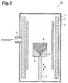
- Fig. 2 is a diagram showing the structure of a crystal growth furnace wherein crystal growth of BaMgF 4 is accomplished.
- the hermetically sealable crystal growth furnace 10 shown in Fig. 2 has a double structure water-cooled by a SUS chamber 1.
- the SUS chamber 1 is provided with a container 6 in which crystal growth is accomplished, and a pair of heaters 3 situated sandwiching and facing the container 6.
- a seed crystal 5 as the starting material for the BaMgF 4 crystal, and a starting mixture 4.
- the container 6 is placed at a prescribed height position in the chamber 1, by being mounted on a shaft 7 connected to the bottom part of the chamber 1.
- the heaters 3 are formed along the side walls of the chamber 1, and between the heaters 3 and the side walls of the chamber 1 there are respectively provided heat-insulating materials 2 to block the heat from the heaters 3.
- the shaft 7 is water-cooled to prevent heat-induced deformation.
- the container 6 in the crystal growth furnace 10 is movable in the vertical direction by the shaft 7, i.e. upwards and downwards along the movement direction axis D shown in Fig. 2 .
- Heating with the heaters 3 that are outside of the container 6 produces a temperature gradient inside the crystal growth furnace 10 along the movement direction axis D. Due to this temperature gradient, the upper part in the crystal growth furnace 10 is at a higher temperature than the lower part.
- a ferroelectric fluoride single crystal can be produced by the vertical Bridgman method, using the crystal growth furnace 10 having such a construction.
- the container 6 used may be a carbon or metal crucible that can be used in the vertical Bridgman method.
- first starting materials with a purity of 99.9% or greater for formation of BaMgF 4 are prepared, and are mixed with a scavenger in the stoichiometric ratio of BaMgF 4 , to obtain a starting mixture 4.
- the container 6 is set on the shaft 7 and disposed in the chamber 1.
- the BaMgF 4 seed crystal 5 is placed below the starting mixture 4 in the container 6.
- the chamber 1 preferably has a water-cooled double structure, composed of SUS.
- the shaft 7 is also preferably water-cooled. This can prevent deformation of the chamber 1 or shaft 7 caused by heat from the heating described hereunder. Also, by water-cooling the shaft 7 it is possible to efficiently draw latent heat from the solidified material in the container 6.
- the chamber 1 is closed and a vacuum system comprising an oil rotary pump or oil diffusion pump is used to create a vacuum in the chamber 1.
- the heaters 3 are operated to increase the temperature in the chamber 1.
- the heaters 3 are set so that the temperature increases from lower positions to higher positions.
- the container 6 is set at a low position and heated at a relatively low temperature.
- the container 6 is raised and heated at a higher temperature. The heating temperature is gradually increased in this manner. Movement of the container 6 can be accomplished by raising and lowering the shaft 7.
- the starting mixture 4 in the container 6 begins to gradually melt from the top.
- the container 6 is further raised, eventually reaching a position where the interface between the starting mixture 4 and seed crystal 5 in the container 6 is a solid-liquid interface, raising of the container 6 is stopped and the material in the container is allowed to stand for several hours until it becomes uniform. After a prescribed period of time has elapsed, the container 6 is gradually lowered to grow a crystal while the solid-liquid interface gradually moves upward.
- the container 6 may be fixed at a prescribed position and the temperature surrounding the container 6 continuously varied to accomplish crystal growth from the position of the seed crystal 5.
- the container Upon completion of crystal growth it is slowly cooled, and upon reaching room temperature, the pressure is restored by means such as introduction of inert gas into the chamber 1, and the container is removed and the BaMgF 4 single crystal obtained from it.
- the obtained single crystal is removed out of the container 6 and may be provided for cutting and shaping into, for example, a sheet oriented on the c-face.
- the single crystal growth direction of the ferroelectric fluoride single crystal is in the range of no greater than ⁇ 20° from the direction of the a-axis, b-axis or c-axis of the crystal axis, and preferably the growth is in an environment such that the single crystal growth direction and the temperature gradient direction within the range in which the single crystal grows are the same, or such that the angle between them is no greater than ⁇ 20°.
- Such a single crystal can grow if the BaMgF 4 seed crystal 5 placed at the bottom part of the container 6 is situated so that it has a cross-section on the side in contact with the starting mixture 4 that is no greater than ⁇ 20° from the orientation of the a-face, b-face or c-face of the seed crystal, and the seed crystal 5 is placed so that the orientation of that cross-section matches the single crystal growth direction.
- the starting mixture 4 housed in the container 6 may be a mixed powder obtained by combining BaF 2 powder and MgF 2 powder, as fluorine-based compounds, in a molar ratio of 1:1 for the stoichiometric ratio of BaMgF 4 , and further mixing a scavenger therewith.
- the fluorine-based compounds used may be commercially available products, and from the viewpoint of obtaining a ferroelectric fluoride single crystal with adequate transmittance, it is preferred to use compounds with a purity of at least 99.9 wt%.
- the scavenger is an additive substance added to induce fluorination of the trace oxides in the powder of the fluorine-based compounds.
- the scavenger By adding a scavenger to the starting material, it is possible to remove the oxides that can cause coloration or reduced internal transmittance of the fluoride single crystal. However, if the scavenger itself remains in the ferroelectric fluoride single crystal, this can also cause coloration or reduced internal transmittance of the ferroelectric fluoride single crystal. Consequently, the scavenger is preferably added at 0.001-10 wt% with respect to the fluorine-based compounds. This will allow the oxides to be sufficiently removed while adequately reducing residue of the scavenger in the ferroelectric fluoride single crystal.
- Such a single crystal can grow if the NdF 3 seed crystal 5 placed at the bottom part of the container 6 is situated so that it has a cross-section on the side in contact with the starting mixture 4 that is no greater than ⁇ 30° from the orientation of the a-face, b-face or c-face of the seed crystal, and the seed crystal 5 is placed so that the orientation of that cross-section matches the single crystal growth direction.
- the starting mixture 4 housed in the container 6 may be powder comprising at least one type of Nd-containing fluorine-based compound, or a fluoride starting material comprising the solidified powder as a single crystal or polycrystal, which is mixed with a scavenger.
- the Nd-containing fluorine-based compound may be, for example, neodymium fluoride (NdF 3 ).
- the Nd-containing fluorine-based compound used may be a commercially available product, and from the viewpoint of obtaining a ferroelectric fluoride single crystal with adequate transmittance, it is preferred to use a compound with a purity of at least 99.9 wt%.
- the atmosphere in the furnace may instead be exchanged with an inert gas atmosphere of helium gas, argon gas or nitrogen gas, a reducing gas atmosphere such as hydrogen gas, or a fluorine-based gas atmosphere such as CF 4 or C 2 H 5 F, instead of a vacuum.
- the inorganic optical filter 15 consists of a NdF 3 single crystal obtained in this manner is set in the optical path of light emitted from the wavelength conversion element 12, as shown in Fig. 1 .
- the inorganic optical filter 15 removes the fundamental wave 14 included in light emitted from the wavelength conversion element 12, thus allowing adequate output of the second harmonic 13.
- the inorganic optical filter consists of a NdF 3 single crystal according to the invention has a high blocking property for fundamental waves of multiple wavelengths, while having high transparency for their second harmonics.
- conventional wavelength optical filters only have a filter function for a fixed range in a target wavelength range, and in that sense they have been monofunctional and difficult to apply for different types of laser light.
- conventional wavelength optical filters for the region from the visible to the near-infrared range have not had total shielding capacity, i.e. the ability to provide 100% shielding, and even with optical filters rated with transmittance of no greater than 1%, the shielding capacity is often at a low enough level that light can be visually confirmed.
- the light source of the invention can be constructed by combining the optical element of the aforementioned embodiment, with a solid laser that directs laser light to the wavelength conversion element of the optical element.
- the wavelength of the laser light is preferably in the wavelength range with a transmittance of no greater than 3%, and more preferably in a wavelength range of no greater than 1%, in the light transmitting spectrum of the inorganic optical filter.
- Solid lasers that emit such laser light include ruby lasers, YAG lasers, titanium sapphire lasers and the like.
- the light source of this embodiment preferably comprises a titanium sapphire laser as the solid laser, from the viewpoint of low cost and allowing relatively stable oscillation of the second harmonic in the vacuum ultraviolet range.
- the heaters 3 were heated to 1000°C, and the container 6 was gradually increased in temperature to a high-temperature range ( ⁇ 500C) for melting of the mixed powder.
- the container 6 was gradually lowered in temperature to a low-temperature range ( ⁇ 500°C) for crystal growth, and then the crystal growth furnace 10 interior was slowly cooled to obtain an optical material consisting of a BaMgF 4 single crystal.
- a thin sample consisting of a plate crystal oriented on the c-face was taken from the obtained optical material and subjected to periodic polarization reversal with a period of 20-80 nm with respect to the plate crystal, as shown in Fig. 1 , to form a wavelength conversion element.
- the container was lowered at a rate of 0.5 mm/h toward the low-temperature zone which was no higher than about 500°C, and crystal growth was conducted by moving the solid-liquid interface upward.
- the crystal growth furnace 10 interior was then allowed to cool, and upon reaching room temperature, the pressure in the furnace was restored with inert gas or the like.
- the container was removed out to obtain an optical material consisting of a NdF 3 single crystal.
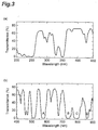
- Fig. 3 shows the light transmitting spectrum of a filter consisting of the NdF 3 single crystal obtained as described above.
- Fig. 3(a) shows the light transmitting spectrum at 200-450 nm
- Fig. 3(b) shows the light transmitting spectrum at 400-900 nm. It was confirmed that in the light transmitting spectrum of the 400-900 nm wavelength range shown in Fig. 3(b) , 4 ranges are present, A, B, C and D, in which the transmittance is no greater than 1%, and several locations had a transmittance of 70% or greater.
- ranges A, B, C and D with transmittances of no greater than 1% were at the range of 565 nm to 585 nm, the range of 726 nm to 747 nm, the range of 778 nm to 812 nm and the range of 855 nm to 870 nm, respectively.
- the half wavelength ranges corresponding to each of these ranges had transmittances of at least 50%.
- the half wavelength ranges corresponding to ranges B and C had transmittances of 70% or greater.
- an inorganic optical filter consisting of a NdF 3 single crystal according to the invention has a function of blocking light with a fundamental wave in any of the wavelength ranges A-D, and transmitting light in the half wavelength range of any of wavelength ranges A-D, as the second harmonic. Since the inorganic optical filter of the invention thus comprises a filter function for multiple wavelength ranges, it can provide flexibility for construction of optical systems. Furthermore, since it is not necessary to combine multiple optical filters, it is possible to achieve smaller size and reduced cost for optical systems.
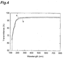
- Fig. 4 shows the light transmitting spectrum of a CaF 2 single crystal and a MgF 2 single crystal, for comparison.
- "a” represents the spectrum of a MgF 2 single crystal
- "b” represents the spectrum of a CaF 2 single crystal. In these light transmitting spectra, no range with transmittance of 1% or lower is seen within 200-800 nm.
- a Dichroic Color Filter (Additive Filters: Red) (thickness: 1 mm), trade name of Thorlabs, was prepared.
- a Camera Lens Color Filter B-440 (thickness: 1 mm), trade name of HOYA Glass, was prepared.
- a wavelength conversion element 1 and a filter 1 were arranged as shown in Fig. 1 , to prepare an optical element.
- the wavelength conversion element 1 of this optical element was irradiated from one end with light of a wavelength of 812 nm using a titanium sapphire laser, as the fundamental wave, and the transmittance and second harmonic transmittance of outputted light from the other end of the wavelength conversion element 1 and outputted light passing through the filter 1 were measured using a vacuum ultraviolet spectrophotometer (KV-201V, by Bunkoukeiki Co., Ltd.).
- the fundamental wave transmittance and second harmonic transmittance of the filter 1 were each calculated by the vacuum ultraviolet spectrophotometer. The results are shown in Table 1.
- the fundamental wave transmittance and second harmonic transmittance were determined in the same manner as Example 1, except that a titanium sapphire laser was used as the laser light source, and light with a wavelength of 792 nm was directed from the end of the wavelength conversion element 1. The results are shown in Table 1.
- the fundamental wave transmittance and second harmonic transmittance were determined in the same manner as Example 1, except that filter C-1 was used instead of the filter 1. The results are shown in Table 1.
- the fundamental wave transmittance and second harmonic transmittance were determined in the same manner as Example 2, except that filter C-1 was used instead of the filter 1. The results are shown in Table 1.
- Example 1 Example 2 Comp. Ex. 1 Comp. Ex. 2 Comp. Ex. 3 Laser light source Titanium sapphire laser Titanium sapphire laser Titanium sapphire laser Titanium sapphire laser Titanium sapphire laser Wavelength conversion element material BaMgF 4 BaMgF 4 BaMgF 4 BaMgF 4 BaMgF 4 Filter Filter 1 Filter 1 Filter C-1 Filter C-1 Filter C-2 Fundamental wavelength (nm) 812 792 812 792 812 Second harmonic (nm) 406 396 406 396 406 Fundamental wavelength transmittance (%) 0.5 0.5 5.2 5.2 3.5 Second harmonic transmittance (%) 99.9 99.9 99.9 99.9 31.0
Landscapes
- Physics & Mathematics (AREA)
- Nonlinear Science (AREA)
- Chemical & Material Sciences (AREA)
- Optics & Photonics (AREA)
- General Physics & Mathematics (AREA)
- Metallurgy (AREA)
- Organic Chemistry (AREA)
- Materials Engineering (AREA)
- Crystallography & Structural Chemistry (AREA)
- Engineering & Computer Science (AREA)
- Inorganic Chemistry (AREA)
- Optical Modulation, Optical Deflection, Nonlinear Optics, Optical Demodulation, Optical Logic Elements (AREA)
- Crystals, And After-Treatments Of Crystals (AREA)
- Optical Filters (AREA)
- Exposure And Positioning Against Photoresist Photosensitive Materials (AREA)
- Exposure Of Semiconductors, Excluding Electron Or Ion Beam Exposure (AREA)
Claims (9)
- Verwendung eines NdF3-Einkristalls als ein anorganisches optisches Filter, um eine Grundwelle von einem Licht zu entfernen, welches von einem Wellenlängen-Umwandlungselement emittiert wird, und um eine zweite Harmonische, welche von der Grundwelle durch das Wellenlängen-Umwandlungselement gewandelt wird, passieren zu lassen.
- Verwendung nach Anspruch 1, wobei das NdF3-Einkristall 4 Wellenlängenbereiche mit einem Transmissionsgrad von nicht größer als 1 % in dem Wellenlängenbereich von 550-900 nm aufweist, und wobei der Transmissionsgrad in jedem der Halbwellenlängenbereiche, welche mit den 4 Wellenlängenbereichen korrespondieren, 50 % oder größer ist.
- Verwendung nach Anspruch 2, wobei die 4 Wellenlängenbereiche in dem Bereich zwischen 565 nm und 585 nm, in dem Bereich zwischen 726 nm und 747 nm, in dem Bereich zwischen 778 nm und 812 nm und in dem Bereich zwischen 855 nm und 870 nm liegen.
- Optisches Element, welches ein Wellenlängen-Umwandlungselement umfasst, wobei einfallendes Licht einer Wellenlängenumwandlung zu dem Zweifachen der Frequenz durch eine Quasi-Phasenanpassung mittels einer primären Anpassung oder einer tertiären Anpassung unterzogen und emittiert wird, und wobei das Wellenlängen-Umwandlungselement aus einem ferroelektrischen Fluorid-Einkristall besteht, welches durch Ba1-y(Mg1-xZnx)1+yF4 repräsentiert ist (wobei -0.2 ≤ x ≤ 1, und - 0,2 ≤ y ≤ 0,2 gelten),
gekennzeichnet durch ein anorganisches optisches Filter, welches in dem optischen Pfad eines Lichts angeordnet ist, das von dem Wellenlängen-Umwandlungselement emittiert wird, wobei das anorganische optische Filter aus einem NdF3-Einkristall besteht. - Optisches Element nach Anspruch 4, wobei das NdF3-Einkristall 4 Wellenlängenbereiche mit einem Transmissionsgrad von nicht größer als 1 % in dem Wellenlängenbereich von 550-900 nm aufweist, wobei der Transmissionsgrad in jedem der Halbwellenlängenbereiche, welche mit den 4 Wellenlängenbereichen korrespondieren, größer als 50 % oder größer ist.
- Optisches Element nach Anspruch 5, wobei die 4 Wellenlängenbereiche in dem Bereich zwischen 565 nm und 585 nm, in dem Bereich zwischen 726 nm und 747 nm, in dem Bereich zwischen 778 nm und 812 nm und in dem Bereich zwischen 855 nm und 870 nm liegen.
- Optisches Element nach einem der Ansprüche 4 bis 6, wobei das ferroelektrische Fluorid-Einkristall ein BaMgF4-Einkristall ist.
- Lichtquelle, welche ein optisches Element nach einem der Ansprüche 4 bis 7 und einen Festkörperlaser umfasst, welcher Laserlicht auf das Wellenlängen-Umwandlungselement des optischen Elements richtet.
- Lichtquelle nach Anspruch 8, wobei die Wellenlänge des Laserlichts in dem Wellenlängenbereich mit einem Transmissionsgrad von nicht größer als 3% in dem Lichtübertragungsspektrum des anorganischen optischen Filters liegt.
Applications Claiming Priority (2)
| Application Number | Priority Date | Filing Date | Title |
|---|---|---|---|
| JP2009225155A JP5515147B2 (ja) | 2009-09-29 | 2009-09-29 | 光学素子及び光源 |
| PCT/JP2010/065833 WO2011040232A1 (ja) | 2009-09-29 | 2010-09-14 | 無機光学フィルター、光学素子及び光源 |
Publications (3)
| Publication Number | Publication Date |
|---|---|
| EP2485071A1 EP2485071A1 (de) | 2012-08-08 |
| EP2485071A4 EP2485071A4 (de) | 2013-04-10 |
| EP2485071B1 true EP2485071B1 (de) | 2016-11-30 |
Family
ID=43826058
Family Applications (1)
| Application Number | Title | Priority Date | Filing Date |
|---|---|---|---|
| EP10820351.4A Not-in-force EP2485071B1 (de) | 2009-09-29 | 2010-09-14 | Anorganischer optischer filter, optisches element und lichtquelle |
Country Status (4)
| Country | Link |
|---|---|
| US (1) | US9217910B2 (de) |
| EP (1) | EP2485071B1 (de) |
| JP (1) | JP5515147B2 (de) |
| WO (1) | WO2011040232A1 (de) |
Families Citing this family (7)
| Publication number | Priority date | Publication date | Assignee | Title |
|---|---|---|---|---|
| EP2692910B1 (de) * | 2011-03-28 | 2023-05-10 | National Institute for Materials Science | Faraday-rotor, optischer isolator und optische verarbeitungsausrüstung |
| US10861690B2 (en) | 2014-10-07 | 2020-12-08 | Consumer Lighting (U.S.), Llc | LED apparatus employing neodymium-fluorine materials |
| US10663143B2 (en) | 2014-10-08 | 2020-05-26 | Consumer Lighting (U.S.), Llc | Materials and optical components for color filtering in a lighting apparatus |
| CN105720163A (zh) | 2014-12-04 | 2016-06-29 | 通用电气照明解决方案有限公司 | 一种照明装置 |
| JP6638292B2 (ja) * | 2015-09-30 | 2020-01-29 | 日亜化学工業株式会社 | 装置光源 |
| WO2017079187A1 (en) * | 2015-11-03 | 2017-05-11 | GE Lighting Solutions, LLC | Color-shifted lamps using neodymium-fluorine containing coating |
| JP7385209B2 (ja) * | 2019-08-21 | 2023-11-22 | 国立大学法人 東京大学 | 真空紫外光の発生方法及びそれに用いる装置 |
Family Cites Families (12)
| Publication number | Priority date | Publication date | Assignee | Title |
|---|---|---|---|---|
| US3982136A (en) * | 1975-07-23 | 1976-09-21 | Bell Telephone Laboratories, Incorporated | Ternary ferroelectric fluoride nonlinear devices |
| JPH0345904A (ja) | 1989-07-13 | 1991-02-27 | Nikon Corp | ファブリ・ペローエタロン |
| US5940417A (en) * | 1992-04-23 | 1999-08-17 | University Of Science And Technology Of China | CsB3 O 5 crystal and its nonlinear optical devices |
| US5339189A (en) | 1993-09-20 | 1994-08-16 | The United States Of America As Represented By The Secretary Of The Navy | Nonlinear frequency conversion optical filter |
| US5646781A (en) | 1995-05-15 | 1997-07-08 | Omega Optical, Inc. | Optical filters for forming enhanced images |
| WO2001002907A1 (en) * | 1999-07-01 | 2001-01-11 | Smith Bruce W | Apparatus and method of image enhancement through spatial filtering |
| JP2005001933A (ja) * | 2003-06-11 | 2005-01-06 | Fujikura Ltd | 金属フッ化物体とその製造方法 |
| JP4605588B2 (ja) | 2003-09-24 | 2011-01-05 | シンジーテック株式会社 | 放射線検出用フッ化物単結晶及びその製造方法並びに放射線検出器 |
| EP1754808B1 (de) * | 2004-04-12 | 2011-06-22 | Stella Chemifa Corporation | Mischkristallmaterial von seltenerdelementfluorid (polykristall und einkristall) und strahlungsdetektor und testvorrichtung |
| JP4630574B2 (ja) | 2004-05-31 | 2011-02-09 | キヤノン株式会社 | 光学素子及びミラー並びに反射防止膜 |
| WO2009069706A1 (ja) * | 2007-11-27 | 2009-06-04 | Hitachi Chemical Company, Ltd. | 光学材料、波長変換素子、強誘電体フッ化物単結晶、及び強誘電体フッ化物単結晶の製造方法 |
| EP2292555A4 (de) | 2008-05-16 | 2012-07-11 | Tokuyama Corp | Vorbehandelte metallfluoride und verfahren zur herstellung von fluoridkristallen |
-
2009
- 2009-09-29 JP JP2009225155A patent/JP5515147B2/ja active Active
-
2010
- 2010-09-14 US US13/498,719 patent/US9217910B2/en not_active Expired - Fee Related
- 2010-09-14 WO PCT/JP2010/065833 patent/WO2011040232A1/ja not_active Ceased
- 2010-09-14 EP EP10820351.4A patent/EP2485071B1/de not_active Not-in-force
Non-Patent Citations (1)
| Title |
|---|
| MARTIN FRIZ ET AL: "Coating Materials 1 Coating Materials for Different Deposition Techniques 2 Requirements for Coating Materials 2.1 Evaporation Materials", OPTICAL INTERFERENCE COATINGS, 1 January 2003 (2003-01-01), pages 105 - 130, XP055206584, Retrieved from the Internet <URL:http://www.thinfilmproducts.umicore.com/Library/LibraryArchive/download_article_coating_materials_12june03.pdf> [retrieved on 20150806] * |
Also Published As
| Publication number | Publication date |
|---|---|
| JP5515147B2 (ja) | 2014-06-11 |
| JP2011075686A (ja) | 2011-04-14 |
| WO2011040232A1 (ja) | 2011-04-07 |
| EP2485071A1 (de) | 2012-08-08 |
| US9217910B2 (en) | 2015-12-22 |
| EP2485071A4 (de) | 2013-04-10 |
| US20120230032A1 (en) | 2012-09-13 |
Similar Documents
| Publication | Publication Date | Title |
|---|---|---|
| US9217910B2 (en) | Inorganic optical filter, optical element, and light source | |
| Lei et al. | Growth of crack-free ZnGeP2 large single crystals for high-power mid-infrared OPO applications | |
| Shimamura et al. | Growth of Ce-doped LiCaAlF6 and LiSrAlF6 single crystals by the Czochralski technique under CF4 atmosphere | |
| CN104532351B (zh) | 一种红外非线性光学晶体材料、其制备方法及应用 | |
| CN114411260A (zh) | 化合物硒铟钠及其非线性光学晶体及其制备方法和用途 | |
| CN117602589A (zh) | 化合物硒镓镁钙和硒镓镁钙红外非线性光学晶体及制备方法和应用 | |
| CN107399722A (zh) | 硒硅银钡和硒硅银钡中远红外非线性光学晶体及制备方法和用途 | |
| CN110578173B (zh) | 一种非线性光学晶体锶锂硅硫及其制备方法与应用 | |
| WO2023109293A1 (zh) | 化合物硼酸锌钙和硼酸锌钙非线性光学晶体及制备方法和用途 | |
| Su et al. | Crystal growth and spectroscopic characterization of Yb-doped and Yb, Na-codoped CaF2 laser crystals by TGT | |
| Zhang et al. | Er3+-doped LuYSGG crystal as a potential 2.79 μm radiation-resistant laser material | |
| Shavelev et al. | Single crystals with advanced laser properties LiCaAlF6: Ce3+ grown by Bridgman technique | |
| Liu et al. | Hydrothermal growth and optical properties of RbBe2BO3F2 crystals | |
| Jesenovec et al. | Homogeneous growth of bulk BaGa4Se7 single crystal and femtosecond laser performance and photodarkening | |
| JP5030861B2 (ja) | 強誘電体フッ化物結晶 | |
| RU2358045C2 (ru) | Керамический лазерный микроструктурированный материал с двойниковой наноструктурой и способ его изготовления | |
| DE102011118229B4 (de) | Verfahren zur Herstellung eines Flourit-Kristalls | |
| CN101230485B (zh) | 一种去除紫外吸收的含铝光学晶体的生长方法 | |
| Xiong et al. | Growth and spectral properties of Er3+: GdVO4 crystal | |
| CN1321228C (zh) | 硼铝酸盐、硼铝酸盐非线性光学晶体及其生长方法和用途 | |
| JP5697002B2 (ja) | 無機光学フィルター | |
| CN117328145A (zh) | 硫镓镁镧红外非线性光学晶体及制备方法和应用 | |
| JPWO2009069706A1 (ja) | 光学材料、波長変換素子、強誘電体フッ化物単結晶、及び強誘電体フッ化物単結晶の製造方法 | |
| Chen et al. | Single crystal growth and nonlinear optical properties of Nd3+ doped STGS crystal for self-frequency-doubling application | |
| CN116639725A (zh) | 系列碱金属稀土硫属卤化物及非线性光学晶体的制备及应用 |
Legal Events
| Date | Code | Title | Description |
|---|---|---|---|
| PUAI | Public reference made under article 153(3) epc to a published international application that has entered the european phase |
Free format text: ORIGINAL CODE: 0009012 |
|
| 17P | Request for examination filed |
Effective date: 20120329 |
|
| AK | Designated contracting states |
Kind code of ref document: A1 Designated state(s): AL AT BE BG CH CY CZ DE DK EE ES FI FR GB GR HR HU IE IS IT LI LT LU LV MC MK MT NL NO PL PT RO SE SI SK SM TR |
|
| DAX | Request for extension of the european patent (deleted) | ||
| A4 | Supplementary search report drawn up and despatched |
Effective date: 20130307 |
|
| RIC1 | Information provided on ipc code assigned before grant |
Ipc: H01L 21/027 20060101ALI20130301BHEP Ipc: C30B 29/12 20060101ALI20130301BHEP Ipc: G02F 1/377 20060101ALI20130301BHEP Ipc: G02B 1/02 20060101ALI20130301BHEP Ipc: G02B 5/22 20060101AFI20130301BHEP Ipc: G02B 5/20 20060101ALI20130301BHEP |
|
| 17Q | First examination report despatched |
Effective date: 20151111 |
|
| GRAP | Despatch of communication of intention to grant a patent |
Free format text: ORIGINAL CODE: EPIDOSNIGR1 |
|
| INTG | Intention to grant announced |
Effective date: 20160530 |
|
| GRAJ | Information related to disapproval of communication of intention to grant by the applicant or resumption of examination proceedings by the epo deleted |
Free format text: ORIGINAL CODE: EPIDOSDIGR1 |
|
| GRAL | Information related to payment of fee for publishing/printing deleted |
Free format text: ORIGINAL CODE: EPIDOSDIGR3 |
|
| GRAS | Grant fee paid |
Free format text: ORIGINAL CODE: EPIDOSNIGR3 |
|
| GRAJ | Information related to disapproval of communication of intention to grant by the applicant or resumption of examination proceedings by the epo deleted |
Free format text: ORIGINAL CODE: EPIDOSDIGR1 |
|
| GRAL | Information related to payment of fee for publishing/printing deleted |
Free format text: ORIGINAL CODE: EPIDOSDIGR3 |
|
| GRAR | Information related to intention to grant a patent recorded |
Free format text: ORIGINAL CODE: EPIDOSNIGR71 |
|
| GRAA | (expected) grant |
Free format text: ORIGINAL CODE: 0009210 |
|
| INTC | Intention to grant announced (deleted) | ||
| AK | Designated contracting states |
Kind code of ref document: B1 Designated state(s): AL AT BE BG CH CY CZ DE DK EE ES FI FR GB GR HR HU IE IS IT LI LT LU LV MC MK MT NL NO PL PT RO SE SI SK SM TR |
|
| INTG | Intention to grant announced |
Effective date: 20161025 |
|
| REG | Reference to a national code |
Ref country code: CH Ref legal event code: EP Ref country code: GB Ref legal event code: FG4D |
|
| RIN1 | Information on inventor provided before grant (corrected) |
Inventor name: VILLORA, GARCIA Inventor name: SUMIYA, KEIJI Inventor name: SHIMAMURA, KIYOSHI |
|
| REG | Reference to a national code |
Ref country code: AT Ref legal event code: REF Ref document number: 850330 Country of ref document: AT Kind code of ref document: T Effective date: 20161215 |
|
| REG | Reference to a national code |
Ref country code: IE Ref legal event code: FG4D |
|
| REG | Reference to a national code |
Ref country code: DE Ref legal event code: R096 Ref document number: 602010038512 Country of ref document: DE |
|
| PG25 | Lapsed in a contracting state [announced via postgrant information from national office to epo] |
Ref country code: LV Free format text: LAPSE BECAUSE OF FAILURE TO SUBMIT A TRANSLATION OF THE DESCRIPTION OR TO PAY THE FEE WITHIN THE PRESCRIBED TIME-LIMIT Effective date: 20161130 |
|
| REG | Reference to a national code |
Ref country code: LT Ref legal event code: MG4D |
|
| REG | Reference to a national code |
Ref country code: NL Ref legal event code: MP Effective date: 20161130 |
|
| REG | Reference to a national code |
Ref country code: AT Ref legal event code: MK05 Ref document number: 850330 Country of ref document: AT Kind code of ref document: T Effective date: 20161130 |
|
| PG25 | Lapsed in a contracting state [announced via postgrant information from national office to epo] |
Ref country code: GR Free format text: LAPSE BECAUSE OF FAILURE TO SUBMIT A TRANSLATION OF THE DESCRIPTION OR TO PAY THE FEE WITHIN THE PRESCRIBED TIME-LIMIT Effective date: 20170301 Ref country code: SE Free format text: LAPSE BECAUSE OF FAILURE TO SUBMIT A TRANSLATION OF THE DESCRIPTION OR TO PAY THE FEE WITHIN THE PRESCRIBED TIME-LIMIT Effective date: 20161130 Ref country code: NO Free format text: LAPSE BECAUSE OF FAILURE TO SUBMIT A TRANSLATION OF THE DESCRIPTION OR TO PAY THE FEE WITHIN THE PRESCRIBED TIME-LIMIT Effective date: 20170228 Ref country code: LT Free format text: LAPSE BECAUSE OF FAILURE TO SUBMIT A TRANSLATION OF THE DESCRIPTION OR TO PAY THE FEE WITHIN THE PRESCRIBED TIME-LIMIT Effective date: 20161130 |
|
| PG25 | Lapsed in a contracting state [announced via postgrant information from national office to epo] |
Ref country code: HR Free format text: LAPSE BECAUSE OF FAILURE TO SUBMIT A TRANSLATION OF THE DESCRIPTION OR TO PAY THE FEE WITHIN THE PRESCRIBED TIME-LIMIT Effective date: 20161130 Ref country code: PL Free format text: LAPSE BECAUSE OF FAILURE TO SUBMIT A TRANSLATION OF THE DESCRIPTION OR TO PAY THE FEE WITHIN THE PRESCRIBED TIME-LIMIT Effective date: 20161130 Ref country code: ES Free format text: LAPSE BECAUSE OF FAILURE TO SUBMIT A TRANSLATION OF THE DESCRIPTION OR TO PAY THE FEE WITHIN THE PRESCRIBED TIME-LIMIT Effective date: 20161130 Ref country code: AT Free format text: LAPSE BECAUSE OF FAILURE TO SUBMIT A TRANSLATION OF THE DESCRIPTION OR TO PAY THE FEE WITHIN THE PRESCRIBED TIME-LIMIT Effective date: 20161130 Ref country code: FI Free format text: LAPSE BECAUSE OF FAILURE TO SUBMIT A TRANSLATION OF THE DESCRIPTION OR TO PAY THE FEE WITHIN THE PRESCRIBED TIME-LIMIT Effective date: 20161130 Ref country code: PT Free format text: LAPSE BECAUSE OF FAILURE TO SUBMIT A TRANSLATION OF THE DESCRIPTION OR TO PAY THE FEE WITHIN THE PRESCRIBED TIME-LIMIT Effective date: 20170330 |
|
| PG25 | Lapsed in a contracting state [announced via postgrant information from national office to epo] |
Ref country code: NL Free format text: LAPSE BECAUSE OF FAILURE TO SUBMIT A TRANSLATION OF THE DESCRIPTION OR TO PAY THE FEE WITHIN THE PRESCRIBED TIME-LIMIT Effective date: 20161130 |
|
| PG25 | Lapsed in a contracting state [announced via postgrant information from national office to epo] |
Ref country code: DK Free format text: LAPSE BECAUSE OF FAILURE TO SUBMIT A TRANSLATION OF THE DESCRIPTION OR TO PAY THE FEE WITHIN THE PRESCRIBED TIME-LIMIT Effective date: 20161130 Ref country code: EE Free format text: LAPSE BECAUSE OF FAILURE TO SUBMIT A TRANSLATION OF THE DESCRIPTION OR TO PAY THE FEE WITHIN THE PRESCRIBED TIME-LIMIT Effective date: 20161130 Ref country code: CZ Free format text: LAPSE BECAUSE OF FAILURE TO SUBMIT A TRANSLATION OF THE DESCRIPTION OR TO PAY THE FEE WITHIN THE PRESCRIBED TIME-LIMIT Effective date: 20161130 Ref country code: SK Free format text: LAPSE BECAUSE OF FAILURE TO SUBMIT A TRANSLATION OF THE DESCRIPTION OR TO PAY THE FEE WITHIN THE PRESCRIBED TIME-LIMIT Effective date: 20161130 Ref country code: RO Free format text: LAPSE BECAUSE OF FAILURE TO SUBMIT A TRANSLATION OF THE DESCRIPTION OR TO PAY THE FEE WITHIN THE PRESCRIBED TIME-LIMIT Effective date: 20161130 |
|
| REG | Reference to a national code |
Ref country code: FR Ref legal event code: PLFP Year of fee payment: 8 |
|
| PG25 | Lapsed in a contracting state [announced via postgrant information from national office to epo] |
Ref country code: BE Free format text: LAPSE BECAUSE OF FAILURE TO SUBMIT A TRANSLATION OF THE DESCRIPTION OR TO PAY THE FEE WITHIN THE PRESCRIBED TIME-LIMIT Effective date: 20161130 Ref country code: IT Free format text: LAPSE BECAUSE OF FAILURE TO SUBMIT A TRANSLATION OF THE DESCRIPTION OR TO PAY THE FEE WITHIN THE PRESCRIBED TIME-LIMIT Effective date: 20161130 Ref country code: SM Free format text: LAPSE BECAUSE OF FAILURE TO SUBMIT A TRANSLATION OF THE DESCRIPTION OR TO PAY THE FEE WITHIN THE PRESCRIBED TIME-LIMIT Effective date: 20161130 Ref country code: BG Free format text: LAPSE BECAUSE OF FAILURE TO SUBMIT A TRANSLATION OF THE DESCRIPTION OR TO PAY THE FEE WITHIN THE PRESCRIBED TIME-LIMIT Effective date: 20170228 |
|
| REG | Reference to a national code |
Ref country code: DE Ref legal event code: R097 Ref document number: 602010038512 Country of ref document: DE |
|
| PLBE | No opposition filed within time limit |
Free format text: ORIGINAL CODE: 0009261 |
|
| STAA | Information on the status of an ep patent application or granted ep patent |
Free format text: STATUS: NO OPPOSITION FILED WITHIN TIME LIMIT |
|
| 26N | No opposition filed |
Effective date: 20170831 |
|
| PG25 | Lapsed in a contracting state [announced via postgrant information from national office to epo] |
Ref country code: SI Free format text: LAPSE BECAUSE OF FAILURE TO SUBMIT A TRANSLATION OF THE DESCRIPTION OR TO PAY THE FEE WITHIN THE PRESCRIBED TIME-LIMIT Effective date: 20161130 |
|
| REG | Reference to a national code |
Ref country code: CH Ref legal event code: PL |
|
| GBPC | Gb: european patent ceased through non-payment of renewal fee |
Effective date: 20170914 |
|
| PG25 | Lapsed in a contracting state [announced via postgrant information from national office to epo] |
Ref country code: MC Free format text: LAPSE BECAUSE OF FAILURE TO SUBMIT A TRANSLATION OF THE DESCRIPTION OR TO PAY THE FEE WITHIN THE PRESCRIBED TIME-LIMIT Effective date: 20161130 |
|
| REG | Reference to a national code |
Ref country code: IE Ref legal event code: MM4A |
|
| PG25 | Lapsed in a contracting state [announced via postgrant information from national office to epo] |
Ref country code: LU Free format text: LAPSE BECAUSE OF NON-PAYMENT OF DUE FEES Effective date: 20170914 |
|
| PG25 | Lapsed in a contracting state [announced via postgrant information from national office to epo] |
Ref country code: CH Free format text: LAPSE BECAUSE OF NON-PAYMENT OF DUE FEES Effective date: 20170930 Ref country code: LI Free format text: LAPSE BECAUSE OF NON-PAYMENT OF DUE FEES Effective date: 20170930 Ref country code: GB Free format text: LAPSE BECAUSE OF NON-PAYMENT OF DUE FEES Effective date: 20170914 Ref country code: IE Free format text: LAPSE BECAUSE OF NON-PAYMENT OF DUE FEES Effective date: 20170914 |
|
| REG | Reference to a national code |
Ref country code: FR Ref legal event code: PLFP Year of fee payment: 9 |
|
| PG25 | Lapsed in a contracting state [announced via postgrant information from national office to epo] |
Ref country code: MT Free format text: LAPSE BECAUSE OF NON-PAYMENT OF DUE FEES Effective date: 20170914 |
|
| PGFP | Annual fee paid to national office [announced via postgrant information from national office to epo] |
Ref country code: DE Payment date: 20180904 Year of fee payment: 9 Ref country code: FR Payment date: 20180813 Year of fee payment: 9 |
|
| PG25 | Lapsed in a contracting state [announced via postgrant information from national office to epo] |
Ref country code: HU Free format text: LAPSE BECAUSE OF FAILURE TO SUBMIT A TRANSLATION OF THE DESCRIPTION OR TO PAY THE FEE WITHIN THE PRESCRIBED TIME-LIMIT; INVALID AB INITIO Effective date: 20100914 |
|
| PG25 | Lapsed in a contracting state [announced via postgrant information from national office to epo] |
Ref country code: CY Free format text: LAPSE BECAUSE OF NON-PAYMENT OF DUE FEES Effective date: 20161130 |
|
| PG25 | Lapsed in a contracting state [announced via postgrant information from national office to epo] |
Ref country code: MK Free format text: LAPSE BECAUSE OF FAILURE TO SUBMIT A TRANSLATION OF THE DESCRIPTION OR TO PAY THE FEE WITHIN THE PRESCRIBED TIME-LIMIT Effective date: 20161130 |
|
| PG25 | Lapsed in a contracting state [announced via postgrant information from national office to epo] |
Ref country code: TR Free format text: LAPSE BECAUSE OF FAILURE TO SUBMIT A TRANSLATION OF THE DESCRIPTION OR TO PAY THE FEE WITHIN THE PRESCRIBED TIME-LIMIT Effective date: 20161130 |
|
| REG | Reference to a national code |
Ref country code: DE Ref legal event code: R119 Ref document number: 602010038512 Country of ref document: DE |
|
| PG25 | Lapsed in a contracting state [announced via postgrant information from national office to epo] |
Ref country code: AL Free format text: LAPSE BECAUSE OF FAILURE TO SUBMIT A TRANSLATION OF THE DESCRIPTION OR TO PAY THE FEE WITHIN THE PRESCRIBED TIME-LIMIT Effective date: 20161130 Ref country code: DE Free format text: LAPSE BECAUSE OF NON-PAYMENT OF DUE FEES Effective date: 20200401 Ref country code: IS Free format text: LAPSE BECAUSE OF FAILURE TO SUBMIT A TRANSLATION OF THE DESCRIPTION OR TO PAY THE FEE WITHIN THE PRESCRIBED TIME-LIMIT Effective date: 20170330 |
|
| PG25 | Lapsed in a contracting state [announced via postgrant information from national office to epo] |
Ref country code: FR Free format text: LAPSE BECAUSE OF NON-PAYMENT OF DUE FEES Effective date: 20190930 |