EP2482372A2 - Leiterplatte und Verfahren zu ihrer Herstellung sowie Brennstoffzelle - Google Patents
Leiterplatte und Verfahren zu ihrer Herstellung sowie Brennstoffzelle Download PDFInfo
- Publication number
- EP2482372A2 EP2482372A2 EP11190710A EP11190710A EP2482372A2 EP 2482372 A2 EP2482372 A2 EP 2482372A2 EP 11190710 A EP11190710 A EP 11190710A EP 11190710 A EP11190710 A EP 11190710A EP 2482372 A2 EP2482372 A2 EP 2482372A2
- Authority
- EP
- European Patent Office
- Prior art keywords
- layer
- printed circuit
- conductor layer
- circuit board
- conductor
- Prior art date
- Legal status (The legal status is an assumption and is not a legal conclusion. Google has not performed a legal analysis and makes no representation as to the accuracy of the status listed.)
- Withdrawn
Links
- 239000000446 fuel Substances 0.000 title claims description 54
- 238000000034 method Methods 0.000 title claims description 46
- 238000004519 manufacturing process Methods 0.000 title claims description 29
- 239000004020 conductor Substances 0.000 claims abstract description 217
- 230000004888 barrier function Effects 0.000 claims abstract description 99
- 238000005260 corrosion Methods 0.000 claims abstract description 33
- 230000007797 corrosion Effects 0.000 claims abstract description 33
- 239000002253 acid Substances 0.000 claims abstract description 16
- 150000007513 acids Chemical class 0.000 claims abstract description 16
- 239000002243 precursor Substances 0.000 claims description 58
- 150000002391 heterocyclic compounds Chemical class 0.000 claims description 36
- 239000011342 resin composition Substances 0.000 claims description 21
- 150000003536 tetrazoles Chemical class 0.000 claims description 11
- 229920000647 polyepoxide Polymers 0.000 claims description 8
- 229920001721 polyimide Polymers 0.000 claims description 8
- 125000001424 substituent group Chemical group 0.000 claims description 8
- IJGRMHOSHXDMSA-UHFFFAOYSA-N Atomic nitrogen Chemical compound N#N IJGRMHOSHXDMSA-UHFFFAOYSA-N 0.000 claims description 6
- KAESVJOAVNADME-UHFFFAOYSA-N Pyrrole Chemical compound C=1C=CNC=1 KAESVJOAVNADME-UHFFFAOYSA-N 0.000 claims description 6
- 239000003822 epoxy resin Substances 0.000 claims description 6
- 125000004435 hydrogen atom Chemical group [H]* 0.000 claims description 6
- 239000005011 phenolic resin Substances 0.000 claims description 6
- 150000001875 compounds Chemical class 0.000 claims description 5
- 229920001225 polyester resin Polymers 0.000 claims description 5
- 239000004645 polyester resin Substances 0.000 claims description 5
- WTKZEGDFNFYCGP-UHFFFAOYSA-N Pyrazole Chemical class C=1C=NNC=1 WTKZEGDFNFYCGP-UHFFFAOYSA-N 0.000 claims description 4
- MZWDAEVXPZRJTQ-WUXMJOGZSA-N 4-[(e)-(4-fluorophenyl)methylideneamino]-3-methyl-1h-1,2,4-triazole-5-thione Chemical compound CC1=NNC(=S)N1\N=C\C1=CC=C(F)C=C1 MZWDAEVXPZRJTQ-WUXMJOGZSA-N 0.000 claims description 3
- 239000003575 carbonaceous material Substances 0.000 claims description 3
- 239000007769 metal material Substances 0.000 claims description 3
- 229910052757 nitrogen Inorganic materials 0.000 claims description 3
- 239000009719 polyimide resin Substances 0.000 claims description 3
- 229920005749 polyurethane resin Polymers 0.000 claims description 3
- 150000004867 thiadiazoles Chemical class 0.000 claims description 3
- 238000010438 heat treatment Methods 0.000 claims description 2
- 238000002156 mixing Methods 0.000 claims description 2
- 125000003354 benzotriazolyl group Chemical class N1N=NC2=C1C=CC=C2* 0.000 claims 1
- 239000010410 layer Substances 0.000 description 392
- BDAGIHXWWSANSR-UHFFFAOYSA-N methanoic acid Natural products OC=O BDAGIHXWWSANSR-UHFFFAOYSA-N 0.000 description 72
- OSWFIVFLDKOXQC-UHFFFAOYSA-N 4-(3-methoxyphenyl)aniline Chemical compound COC1=CC=CC(C=2C=CC(N)=CC=2)=C1 OSWFIVFLDKOXQC-UHFFFAOYSA-N 0.000 description 36
- 235000019253 formic acid Nutrition 0.000 description 36
- OKKJLVBELUTLKV-UHFFFAOYSA-N Methanol Chemical compound OC OKKJLVBELUTLKV-UHFFFAOYSA-N 0.000 description 24
- 230000000052 comparative effect Effects 0.000 description 19
- 238000007654 immersion Methods 0.000 description 16
- 239000000203 mixture Substances 0.000 description 16
- OKTJSMMVPCPJKN-UHFFFAOYSA-N Carbon Chemical compound [C] OKTJSMMVPCPJKN-UHFFFAOYSA-N 0.000 description 13
- -1 hydrogen ions Chemical class 0.000 description 13
- MARUHZGHZWCEQU-UHFFFAOYSA-N 5-phenyl-2h-tetrazole Chemical class C1=CC=CC=C1C1=NNN=N1 MARUHZGHZWCEQU-UHFFFAOYSA-N 0.000 description 12
- 239000010439 graphite Substances 0.000 description 10
- 229910002804 graphite Inorganic materials 0.000 description 10
- VNWKTOKETHGBQD-UHFFFAOYSA-N methane Chemical compound C VNWKTOKETHGBQD-UHFFFAOYSA-N 0.000 description 7
- ZWEHNKRNPOVVGH-UHFFFAOYSA-N 2-Butanone Chemical compound CCC(C)=O ZWEHNKRNPOVVGH-UHFFFAOYSA-N 0.000 description 6
- LRUDIIUSNGCQKF-UHFFFAOYSA-N 5-methyl-1H-benzotriazole Chemical class C1=C(C)C=CC2=NNN=C21 LRUDIIUSNGCQKF-UHFFFAOYSA-N 0.000 description 6
- 238000012545 processing Methods 0.000 description 6
- KLSJWNVTNUYHDU-UHFFFAOYSA-N Amitrole Chemical compound NC1=NC=NN1 KLSJWNVTNUYHDU-UHFFFAOYSA-N 0.000 description 5
- RYGMFSIKBFXOCR-UHFFFAOYSA-N Copper Chemical compound [Cu] RYGMFSIKBFXOCR-UHFFFAOYSA-N 0.000 description 5
- 239000004642 Polyimide Substances 0.000 description 5
- 150000001565 benzotriazoles Chemical class 0.000 description 5
- 239000006227 byproduct Substances 0.000 description 5
- 229910052802 copper Inorganic materials 0.000 description 5
- 239000010949 copper Substances 0.000 description 5
- 238000005530 etching Methods 0.000 description 5
- 239000001257 hydrogen Substances 0.000 description 5
- 229910052739 hydrogen Inorganic materials 0.000 description 5
- 239000000463 material Substances 0.000 description 5
- 239000000126 substance Substances 0.000 description 5
- 239000003792 electrolyte Substances 0.000 description 4
- 239000010931 gold Substances 0.000 description 4
- CMGDVUCDZOBDNL-UHFFFAOYSA-N 4-methyl-2h-benzotriazole Chemical class CC1=CC=CC2=NNN=C12 CMGDVUCDZOBDNL-UHFFFAOYSA-N 0.000 description 3
- XZGLNCKSNVGDNX-UHFFFAOYSA-N 5-methyl-2h-tetrazole Chemical class CC=1N=NNN=1 XZGLNCKSNVGDNX-UHFFFAOYSA-N 0.000 description 3
- LYCAIKOWRPUZTN-UHFFFAOYSA-N Ethylene glycol Chemical compound OCCO LYCAIKOWRPUZTN-UHFFFAOYSA-N 0.000 description 3
- 241000282320 Panthera leo Species 0.000 description 3
- 239000004962 Polyamide-imide Substances 0.000 description 3
- BQCADISMDOOEFD-UHFFFAOYSA-N Silver Chemical compound [Ag] BQCADISMDOOEFD-UHFFFAOYSA-N 0.000 description 3
- 238000001035 drying Methods 0.000 description 3
- RAXXELZNTBOGNW-UHFFFAOYSA-N imidazole Natural products C1=CNC=N1 RAXXELZNTBOGNW-UHFFFAOYSA-N 0.000 description 3
- 150000002500 ions Chemical group 0.000 description 3
- 239000003273 ketjen black Substances 0.000 description 3
- 125000001997 phenyl group Chemical group [H]C1=C([H])C([H])=C(*)C([H])=C1[H] 0.000 description 3
- 229920002312 polyamide-imide Polymers 0.000 description 3
- 239000011148 porous material Substances 0.000 description 3
- 229920005989 resin Polymers 0.000 description 3
- 239000011347 resin Substances 0.000 description 3
- 239000004925 Acrylic resin Substances 0.000 description 2
- CURLTUGMZLYLDI-UHFFFAOYSA-N Carbon dioxide Chemical compound O=C=O CURLTUGMZLYLDI-UHFFFAOYSA-N 0.000 description 2
- 239000004593 Epoxy Substances 0.000 description 2
- 229910021578 Iron(III) chloride Inorganic materials 0.000 description 2
- 229920000106 Liquid crystal polymer Polymers 0.000 description 2
- 239000004977 Liquid-crystal polymers (LCPs) Substances 0.000 description 2
- 239000004734 Polyphenylene sulfide Substances 0.000 description 2
- 125000003545 alkoxy group Chemical group 0.000 description 2
- 125000004453 alkoxycarbonyl group Chemical group 0.000 description 2
- 125000003282 alkyl amino group Chemical group 0.000 description 2
- 125000000217 alkyl group Chemical group 0.000 description 2
- 125000003277 amino group Chemical group 0.000 description 2
- 125000003118 aryl group Chemical group 0.000 description 2
- QVGXLLKOCUKJST-UHFFFAOYSA-N atomic oxygen Chemical compound [O] QVGXLLKOCUKJST-UHFFFAOYSA-N 0.000 description 2
- 229910052799 carbon Inorganic materials 0.000 description 2
- 125000003178 carboxy group Chemical group [H]OC(*)=O 0.000 description 2
- 239000003054 catalyst Substances 0.000 description 2
- 239000013256 coordination polymer Substances 0.000 description 2
- 229920000295 expanded polytetrafluoroethylene Polymers 0.000 description 2
- 125000000524 functional group Chemical group 0.000 description 2
- 238000007429 general method Methods 0.000 description 2
- PCHJSUWPFVWCPO-UHFFFAOYSA-N gold Chemical compound [Au] PCHJSUWPFVWCPO-UHFFFAOYSA-N 0.000 description 2
- 229910052737 gold Inorganic materials 0.000 description 2
- 239000011810 insulating material Substances 0.000 description 2
- RBTARNINKXHZNM-UHFFFAOYSA-K iron trichloride Chemical compound Cl[Fe](Cl)Cl RBTARNINKXHZNM-UHFFFAOYSA-K 0.000 description 2
- 239000007788 liquid Substances 0.000 description 2
- 238000005259 measurement Methods 0.000 description 2
- 239000012528 membrane Substances 0.000 description 2
- 239000001301 oxygen Substances 0.000 description 2
- 229910052760 oxygen Inorganic materials 0.000 description 2
- 230000002093 peripheral effect Effects 0.000 description 2
- BASFCYQUMIYNBI-UHFFFAOYSA-N platinum Chemical compound [Pt] BASFCYQUMIYNBI-UHFFFAOYSA-N 0.000 description 2
- 229920003207 poly(ethylene-2,6-naphthalate) Polymers 0.000 description 2
- 239000011112 polyethylene naphthalate Substances 0.000 description 2
- 229920000139 polyethylene terephthalate Polymers 0.000 description 2
- 239000005020 polyethylene terephthalate Substances 0.000 description 2
- 229920000098 polyolefin Polymers 0.000 description 2
- 229920000069 polyphenylene sulfide Polymers 0.000 description 2
- 229920001343 polytetrafluoroethylene Polymers 0.000 description 2
- 239000004810 polytetrafluoroethylene Substances 0.000 description 2
- CXMXRPHRNRROMY-UHFFFAOYSA-N sebacic acid Chemical compound OC(=O)CCCCCCCCC(O)=O CXMXRPHRNRROMY-UHFFFAOYSA-N 0.000 description 2
- 229910052709 silver Inorganic materials 0.000 description 2
- 239000004332 silver Substances 0.000 description 2
- 239000000758 substrate Substances 0.000 description 2
- 125000003396 thiol group Chemical group [H]S* 0.000 description 2
- 0 *C1N(*)N=NN1 Chemical compound *C1N(*)N=NN1 0.000 description 1
- QWENRTYMTSOGBR-UHFFFAOYSA-N 1H-1,2,3-Triazole Chemical class C=1C=NNN=1 QWENRTYMTSOGBR-UHFFFAOYSA-N 0.000 description 1
- KJUGUADJHNHALS-UHFFFAOYSA-N 1H-tetrazole Chemical class C=1N=NNN=1 KJUGUADJHNHALS-UHFFFAOYSA-N 0.000 description 1
- NSPMIYGKQJPBQR-CVMUNTFWSA-N 1h-1,2,4-triazole Chemical class [13CH]=1[15N]=[13CH][15NH][15N]=1 NSPMIYGKQJPBQR-CVMUNTFWSA-N 0.000 description 1
- RYRZSXJVEILFRR-UHFFFAOYSA-N 2,3-dimethylterephthalic acid Chemical compound CC1=C(C)C(C(O)=O)=CC=C1C(O)=O RYRZSXJVEILFRR-UHFFFAOYSA-N 0.000 description 1
- FPZWZCWUIYYYBU-UHFFFAOYSA-N 2-(2-ethoxyethoxy)ethyl acetate Chemical compound CCOCCOCCOC(C)=O FPZWZCWUIYYYBU-UHFFFAOYSA-N 0.000 description 1
- LHPPDQUVECZQSW-UHFFFAOYSA-N 2-(benzotriazol-2-yl)-4,6-ditert-butylphenol Chemical class CC(C)(C)C1=CC(C(C)(C)C)=CC(N2N=C3C=CC=CC3=N2)=C1O LHPPDQUVECZQSW-UHFFFAOYSA-N 0.000 description 1
- UJBXVTJYSIDCIE-UHFFFAOYSA-N 2-[(2-sulfanylidene-3h-1,3,4-thiadiazol-5-yl)sulfanyl]acetic acid Chemical class OC(=O)CSC1=NNC(=S)S1 UJBXVTJYSIDCIE-UHFFFAOYSA-N 0.000 description 1
- KFJDQPJLANOOOB-UHFFFAOYSA-N 2h-benzotriazole-4-carboxylic acid Chemical class OC(=O)C1=CC=CC2=NNN=C12 KFJDQPJLANOOOB-UHFFFAOYSA-N 0.000 description 1
- GUOVBFFLXKJFEE-UHFFFAOYSA-N 2h-benzotriazole-5-carboxylic acid Chemical compound C1=C(C(=O)O)C=CC2=NNN=C21 GUOVBFFLXKJFEE-UHFFFAOYSA-N 0.000 description 1
- ULRPISSMEBPJLN-UHFFFAOYSA-N 2h-tetrazol-5-amine Chemical class NC1=NN=NN1 ULRPISSMEBPJLN-UHFFFAOYSA-N 0.000 description 1
- TZFOEYRGARRRGO-UHFFFAOYSA-N 2h-triazole-4,5-dicarboxylic acid Chemical compound OC(=O)C1=NNN=C1C(O)=O TZFOEYRGARRRGO-UHFFFAOYSA-N 0.000 description 1
- HAYIPGIFANTODX-UHFFFAOYSA-N 4,6-dimethylbenzene-1,3-dicarboxylic acid Chemical compound CC1=CC(C)=C(C(O)=O)C=C1C(O)=O HAYIPGIFANTODX-UHFFFAOYSA-N 0.000 description 1
- 229920000178 Acrylic resin Polymers 0.000 description 1
- 229910001316 Ag alloy Inorganic materials 0.000 description 1
- 229910000838 Al alloy Inorganic materials 0.000 description 1
- 229920006310 Asahi-Kasei Polymers 0.000 description 1
- 229910001020 Au alloy Inorganic materials 0.000 description 1
- 229920000049 Carbon (fiber) Polymers 0.000 description 1
- 229910000881 Cu alloy Inorganic materials 0.000 description 1
- 239000005057 Hexamethylene diisocyanate Substances 0.000 description 1
- WHXSMMKQMYFTQS-UHFFFAOYSA-N Lithium Chemical compound [Li] WHXSMMKQMYFTQS-UHFFFAOYSA-N 0.000 description 1
- 239000004697 Polyetherimide Substances 0.000 description 1
- 239000004698 Polyethylene Substances 0.000 description 1
- 239000004743 Polypropylene Substances 0.000 description 1
- 229910001260 Pt alloy Inorganic materials 0.000 description 1
- 229910004530 SIMS 5 Inorganic materials 0.000 description 1
- 229910001069 Ti alloy Inorganic materials 0.000 description 1
- RTAQQCXQSZGOHL-UHFFFAOYSA-N Titanium Chemical compound [Ti] RTAQQCXQSZGOHL-UHFFFAOYSA-N 0.000 description 1
- 150000008065 acid anhydrides Chemical class 0.000 description 1
- 239000000654 additive Substances 0.000 description 1
- 239000000853 adhesive Substances 0.000 description 1
- 230000001070 adhesive effect Effects 0.000 description 1
- 229910045601 alloy Inorganic materials 0.000 description 1
- 239000000956 alloy Substances 0.000 description 1
- 229910052782 aluminium Inorganic materials 0.000 description 1
- XAGFODPZIPBFFR-UHFFFAOYSA-N aluminium Chemical compound [Al] XAGFODPZIPBFFR-UHFFFAOYSA-N 0.000 description 1
- 238000004458 analytical method Methods 0.000 description 1
- 239000012298 atmosphere Substances 0.000 description 1
- 239000004841 bisphenol A epoxy resin Substances 0.000 description 1
- YHWCPXVTRSHPNY-UHFFFAOYSA-N butan-1-olate;titanium(4+) Chemical compound [Ti+4].CCCC[O-].CCCC[O-].CCCC[O-].CCCC[O-] YHWCPXVTRSHPNY-UHFFFAOYSA-N 0.000 description 1
- 239000006229 carbon black Substances 0.000 description 1
- 239000001569 carbon dioxide Substances 0.000 description 1
- 229910002092 carbon dioxide Inorganic materials 0.000 description 1
- 239000004917 carbon fiber Substances 0.000 description 1
- 239000002041 carbon nanotube Substances 0.000 description 1
- 229910021393 carbon nanotube Inorganic materials 0.000 description 1
- 239000003795 chemical substances by application Substances 0.000 description 1
- 239000011247 coating layer Substances 0.000 description 1
- 229920001940 conductive polymer Polymers 0.000 description 1
- 238000006297 dehydration reaction Methods 0.000 description 1
- XXJWXESWEXIICW-UHFFFAOYSA-N diethylene glycol monoethyl ether Chemical compound CCOCCOCCO XXJWXESWEXIICW-UHFFFAOYSA-N 0.000 description 1
- 238000007598 dipping method Methods 0.000 description 1
- 230000000694 effects Effects 0.000 description 1
- 150000002148 esters Chemical group 0.000 description 1
- 238000001704 evaporation Methods 0.000 description 1
- 230000008020 evaporation Effects 0.000 description 1
- 239000003353 gold alloy Substances 0.000 description 1
- 238000007756 gravure coating Methods 0.000 description 1
- PKWIYNIDEDLDCJ-UHFFFAOYSA-N guanazole Chemical class NC1=NNC(N)=N1 PKWIYNIDEDLDCJ-UHFFFAOYSA-N 0.000 description 1
- RRAMGCGOFNQTLD-UHFFFAOYSA-N hexamethylene diisocyanate Chemical compound O=C=NCCCCCCN=C=O RRAMGCGOFNQTLD-UHFFFAOYSA-N 0.000 description 1
- 150000002460 imidazoles Chemical class 0.000 description 1
- 229910052744 lithium Inorganic materials 0.000 description 1
- 229910052751 metal Inorganic materials 0.000 description 1
- 239000002184 metal Substances 0.000 description 1
- 230000004048 modification Effects 0.000 description 1
- 238000012986 modification Methods 0.000 description 1
- SLCVBVWXLSEKPL-UHFFFAOYSA-N neopentyl glycol Chemical compound OCC(C)(C)CO SLCVBVWXLSEKPL-UHFFFAOYSA-N 0.000 description 1
- 239000002245 particle Substances 0.000 description 1
- 230000035699 permeability Effects 0.000 description 1
- 239000012466 permeate Substances 0.000 description 1
- 238000007747 plating Methods 0.000 description 1
- 229910052697 platinum Inorganic materials 0.000 description 1
- 229920000767 polyaniline Polymers 0.000 description 1
- 229920001601 polyetherimide Polymers 0.000 description 1
- 229920000573 polyethylene Polymers 0.000 description 1
- 239000005518 polymer electrolyte Substances 0.000 description 1
- 239000002861 polymer material Substances 0.000 description 1
- 238000006116 polymerization reaction Methods 0.000 description 1
- 229920001155 polypropylene Polymers 0.000 description 1
- 229920000123 polythiophene Polymers 0.000 description 1
- 238000004080 punching Methods 0.000 description 1
- 150000003217 pyrazoles Chemical class 0.000 description 1
- 229920003987 resole Polymers 0.000 description 1
- 238000005507 spraying Methods 0.000 description 1
- 238000004544 sputter deposition Methods 0.000 description 1
- 150000007979 thiazole derivatives Chemical class 0.000 description 1
- 229910052719 titanium Inorganic materials 0.000 description 1
- 239000010936 titanium Substances 0.000 description 1
- 150000003852 triazoles Chemical class 0.000 description 1
- SRPWOOOHEPICQU-UHFFFAOYSA-N trimellitic anhydride Chemical compound OC(=O)C1=CC=C2C(=O)OC(=O)C2=C1 SRPWOOOHEPICQU-UHFFFAOYSA-N 0.000 description 1
- XLYOFNOQVPJJNP-UHFFFAOYSA-N water Substances O XLYOFNOQVPJJNP-UHFFFAOYSA-N 0.000 description 1
Images


Classifications
-
- H—ELECTRICITY
- H05—ELECTRIC TECHNIQUES NOT OTHERWISE PROVIDED FOR
- H05K—PRINTED CIRCUITS; CASINGS OR CONSTRUCTIONAL DETAILS OF ELECTRIC APPARATUS; MANUFACTURE OF ASSEMBLAGES OF ELECTRICAL COMPONENTS
- H05K1/00—Printed circuits
- H05K1/02—Details
-
- H—ELECTRICITY
- H01—ELECTRIC ELEMENTS
- H01M—PROCESSES OR MEANS, e.g. BATTERIES, FOR THE DIRECT CONVERSION OF CHEMICAL ENERGY INTO ELECTRICAL ENERGY
- H01M8/00—Fuel cells; Manufacture thereof
- H01M8/02—Details
- H01M8/0202—Collectors; Separators, e.g. bipolar separators; Interconnectors
- H01M8/0269—Separators, collectors or interconnectors including a printed circuit board
-
- C—CHEMISTRY; METALLURGY
- C08—ORGANIC MACROMOLECULAR COMPOUNDS; THEIR PREPARATION OR CHEMICAL WORKING-UP; COMPOSITIONS BASED THEREON
- C08K—Use of inorganic or non-macromolecular organic substances as compounding ingredients
- C08K3/00—Use of inorganic substances as compounding ingredients
- C08K3/02—Elements
- C08K3/04—Carbon
-
- C—CHEMISTRY; METALLURGY
- C08—ORGANIC MACROMOLECULAR COMPOUNDS; THEIR PREPARATION OR CHEMICAL WORKING-UP; COMPOSITIONS BASED THEREON
- C08K—Use of inorganic or non-macromolecular organic substances as compounding ingredients
- C08K5/00—Use of organic ingredients
- C08K5/16—Nitrogen-containing compounds
- C08K5/34—Heterocyclic compounds having nitrogen in the ring
- C08K5/3467—Heterocyclic compounds having nitrogen in the ring having more than two nitrogen atoms in the ring
- C08K5/3472—Five-membered rings
-
- H—ELECTRICITY
- H01—ELECTRIC ELEMENTS
- H01M—PROCESSES OR MEANS, e.g. BATTERIES, FOR THE DIRECT CONVERSION OF CHEMICAL ENERGY INTO ELECTRICAL ENERGY
- H01M8/00—Fuel cells; Manufacture thereof
- H01M8/02—Details
- H01M8/0271—Sealing or supporting means around electrodes, matrices or membranes
- H01M8/028—Sealing means characterised by their material
- H01M8/0284—Organic resins; Organic polymers
-
- H—ELECTRICITY
- H01—ELECTRIC ELEMENTS
- H01M—PROCESSES OR MEANS, e.g. BATTERIES, FOR THE DIRECT CONVERSION OF CHEMICAL ENERGY INTO ELECTRICAL ENERGY
- H01M8/00—Fuel cells; Manufacture thereof
- H01M8/02—Details
- H01M8/0271—Sealing or supporting means around electrodes, matrices or membranes
- H01M8/0286—Processes for forming seals
-
- H—ELECTRICITY
- H01—ELECTRIC ELEMENTS
- H01M—PROCESSES OR MEANS, e.g. BATTERIES, FOR THE DIRECT CONVERSION OF CHEMICAL ENERGY INTO ELECTRICAL ENERGY
- H01M8/00—Fuel cells; Manufacture thereof
- H01M8/10—Fuel cells with solid electrolytes
-
- H—ELECTRICITY
- H01—ELECTRIC ELEMENTS
- H01M—PROCESSES OR MEANS, e.g. BATTERIES, FOR THE DIRECT CONVERSION OF CHEMICAL ENERGY INTO ELECTRICAL ENERGY
- H01M8/00—Fuel cells; Manufacture thereof
- H01M8/10—Fuel cells with solid electrolytes
- H01M8/1097—Fuel cells applied on a support, e.g. miniature fuel cells deposited on silica supports
-
- H—ELECTRICITY
- H05—ELECTRIC TECHNIQUES NOT OTHERWISE PROVIDED FOR
- H05K—PRINTED CIRCUITS; CASINGS OR CONSTRUCTIONAL DETAILS OF ELECTRIC APPARATUS; MANUFACTURE OF ASSEMBLAGES OF ELECTRICAL COMPONENTS
- H05K3/00—Apparatus or processes for manufacturing printed circuits
- H05K3/22—Secondary treatment of printed circuits
- H05K3/24—Reinforcing the conductive pattern
-
- H—ELECTRICITY
- H05—ELECTRIC TECHNIQUES NOT OTHERWISE PROVIDED FOR
- H05K—PRINTED CIRCUITS; CASINGS OR CONSTRUCTIONAL DETAILS OF ELECTRIC APPARATUS; MANUFACTURE OF ASSEMBLAGES OF ELECTRICAL COMPONENTS
- H05K3/00—Apparatus or processes for manufacturing printed circuits
- H05K3/22—Secondary treatment of printed circuits
- H05K3/28—Applying non-metallic protective coatings
- H05K3/282—Applying non-metallic protective coatings for inhibiting the corrosion of the circuit, e.g. for preserving the solderability
-
- H—ELECTRICITY
- H05—ELECTRIC TECHNIQUES NOT OTHERWISE PROVIDED FOR
- H05K—PRINTED CIRCUITS; CASINGS OR CONSTRUCTIONAL DETAILS OF ELECTRIC APPARATUS; MANUFACTURE OF ASSEMBLAGES OF ELECTRICAL COMPONENTS
- H05K3/00—Apparatus or processes for manufacturing printed circuits
- H05K3/38—Improvement of the adhesion between the insulating substrate and the metal
-
- H—ELECTRICITY
- H05—ELECTRIC TECHNIQUES NOT OTHERWISE PROVIDED FOR
- H05K—PRINTED CIRCUITS; CASINGS OR CONSTRUCTIONAL DETAILS OF ELECTRIC APPARATUS; MANUFACTURE OF ASSEMBLAGES OF ELECTRICAL COMPONENTS
- H05K1/00—Printed circuits
- H05K1/02—Details
- H05K1/0277—Bendability or stretchability details
- H05K1/028—Bending or folding regions of flexible printed circuits
-
- H—ELECTRICITY
- H05—ELECTRIC TECHNIQUES NOT OTHERWISE PROVIDED FOR
- H05K—PRINTED CIRCUITS; CASINGS OR CONSTRUCTIONAL DETAILS OF ELECTRIC APPARATUS; MANUFACTURE OF ASSEMBLAGES OF ELECTRICAL COMPONENTS
- H05K2201/00—Indexing scheme relating to printed circuits covered by H05K1/00
- H05K2201/01—Dielectrics
- H05K2201/0137—Materials
- H05K2201/0154—Polyimide
-
- H—ELECTRICITY
- H05—ELECTRIC TECHNIQUES NOT OTHERWISE PROVIDED FOR
- H05K—PRINTED CIRCUITS; CASINGS OR CONSTRUCTIONAL DETAILS OF ELECTRIC APPARATUS; MANUFACTURE OF ASSEMBLAGES OF ELECTRICAL COMPONENTS
- H05K2201/00—Indexing scheme relating to printed circuits covered by H05K1/00
- H05K2201/03—Conductive materials
- H05K2201/032—Materials
- H05K2201/0323—Carbon
-
- H—ELECTRICITY
- H05—ELECTRIC TECHNIQUES NOT OTHERWISE PROVIDED FOR
- H05K—PRINTED CIRCUITS; CASINGS OR CONSTRUCTIONAL DETAILS OF ELECTRIC APPARATUS; MANUFACTURE OF ASSEMBLAGES OF ELECTRICAL COMPONENTS
- H05K2201/00—Indexing scheme relating to printed circuits covered by H05K1/00
- H05K2201/05—Flexible printed circuits [FPCs]
- H05K2201/056—Folded around rigid support or component
-
- H—ELECTRICITY
- H05—ELECTRIC TECHNIQUES NOT OTHERWISE PROVIDED FOR
- H05K—PRINTED CIRCUITS; CASINGS OR CONSTRUCTIONAL DETAILS OF ELECTRIC APPARATUS; MANUFACTURE OF ASSEMBLAGES OF ELECTRICAL COMPONENTS
- H05K2203/00—Indexing scheme relating to apparatus or processes for manufacturing printed circuits covered by H05K3/00
- H05K2203/12—Using specific substances
- H05K2203/122—Organic non-polymeric compounds, e.g. oil, wax or thiol
- H05K2203/124—Heterocyclic organic compounds, e.g. azole, furan
-
- Y—GENERAL TAGGING OF NEW TECHNOLOGICAL DEVELOPMENTS; GENERAL TAGGING OF CROSS-SECTIONAL TECHNOLOGIES SPANNING OVER SEVERAL SECTIONS OF THE IPC; TECHNICAL SUBJECTS COVERED BY FORMER USPC CROSS-REFERENCE ART COLLECTIONS [XRACs] AND DIGESTS
- Y02—TECHNOLOGIES OR APPLICATIONS FOR MITIGATION OR ADAPTATION AGAINST CLIMATE CHANGE
- Y02E—REDUCTION OF GREENHOUSE GAS [GHG] EMISSIONS, RELATED TO ENERGY GENERATION, TRANSMISSION OR DISTRIBUTION
- Y02E60/00—Enabling technologies; Technologies with a potential or indirect contribution to GHG emissions mitigation
- Y02E60/30—Hydrogen technology
- Y02E60/50—Fuel cells
-
- Y—GENERAL TAGGING OF NEW TECHNOLOGICAL DEVELOPMENTS; GENERAL TAGGING OF CROSS-SECTIONAL TECHNOLOGIES SPANNING OVER SEVERAL SECTIONS OF THE IPC; TECHNICAL SUBJECTS COVERED BY FORMER USPC CROSS-REFERENCE ART COLLECTIONS [XRACs] AND DIGESTS
- Y02—TECHNOLOGIES OR APPLICATIONS FOR MITIGATION OR ADAPTATION AGAINST CLIMATE CHANGE
- Y02P—CLIMATE CHANGE MITIGATION TECHNOLOGIES IN THE PRODUCTION OR PROCESSING OF GOODS
- Y02P70/00—Climate change mitigation technologies in the production process for final industrial or consumer products
- Y02P70/50—Manufacturing or production processes characterised by the final manufactured product
Definitions
- the present invention relates to a printed circuit board and a method for manufacturing the same, and a fuel cell including the printed circuit board.
- the fuel cells include direct methanol fuel cells.
- methanol is decomposed with a catalyst, to form hydrogen ions.
- the hydrogen ions and oxygen in air are reacted with each other, to generate electric power.
- chemical energy can be significantly efficiently converted into electric energy so that a very high energy density can be obtained.
- JP 2004-200064, A discusses a fuel cell in which a membrane electrode assembly including a fuel electrode, an air electrode, and a polymer electrolyte film is arranged between conductor layers on a substrate.
- the fuel electrode and the air electrode in the membrane electrode assembly and the conductor layers on the substrate are in electric contact with each other.
- a circulation structure for circulating fuel in the fuel electrode and a circulation structure for circulating air in the air electrode are provided.
- the fuel electrode and the air electrode corrode. Therefore, resistances of the fuel electrode and the air electrode are increased. As a result, collection efficiencies of the fuel electrode and the air electrode are reduced.
- the present invention is directed to providing a printed circuit board in which a conductor layer can be prevented from corroding while a resistance of the conductor layer can be reduced, and a method for manufacturing the same, and a fuel cell including the printed circuit board.
- a printed circuit board includes an insulating layer, a conductor layer having a predetermined pattern and having first and second main surfaces and a side surface while being formed on the insulating layer so that the second main surface opposes the insulating layer, a barrier layer formed on at least a partial region of the first main surface and the side surface of the conductor layer and having higher corrosion resistance to acids than that of the conductor layer, and a conductive cover layer that covers the first main surface and the side surface of the conductor layer and the barrier layer.
- the conductor layer having the predetermined pattern is formed on the insulating layer so that the second main surface opposes the insulating layer.
- the barrier layer having higher corrosion resistance to acids than that of the conductor layer is formed on at least the partial region of the first main surface and the side surface of the conductor layer while the first main surface and the side surface of the conductor layer and the barrier layer are covered with the conductive cover layer.
- a by-product such as formic acid in the fuel cell can be prevented from adhering to the conductor layer. Therefore, the conductor layer can be prevented from corroding. A contact resistance between the conductor layer and the cover layer can be prevented from being increased. As a result, electric power of the fuel cell can be efficiently supplied to the exterior.
- the barrier layer may include a heterocyclic compound. In this case, the corrosion resistance to acids of the barrier layer can be easily increased.
- the heterocyclic compound may include nitrogen. In this case, the corrosion resistance to acids of the barrier layer can be more easily increased.
- the heterocyclic compound may include an azole-based compound.
- the corrosion resistance to acids of the barrier layer can be further easily increased.
- the heterocyclic compound may include at least one of a tetrazole derivative, a diazole derivative, a thiadiazole derivative, and a triazole derivative.
- the corrosion resistance to acids of the barrier layer can be further easily increased.
- the heterocyclic compound may include a tetrazole derivative expressed by the following formula (1), where R1 and R2 may be the same as or different from each other, and may be each a hydrogen atom or a substituent group. In this case, the corrosion resistance to acids of the barrier layer can be further easily increased.
- the heterocyclic compound may include a benzotriazole derivative expressed by the following formula (2), where R3 and R4 may be the same as or different from each other, and may be each a hydrogen atom or a substituent group. In this case, the corrosion resistance to acids of the barrier layer can be further easily increased.
- the thickness of the barrier layer may be not less than 1 nm and not more than 1000 nm.
- the conductor layer can be sufficiently prevented from corroding. Adhesiveness between the conductor layer and the cover layer can be improved, and conductivity between the conductor layer and the cover layer can be improved.
- the cover layer may include a resin composition. In this case, flexibility of the printed circuit board is improved.
- the resin composition may include at least one of phenol resin, epoxy resin, polyester resin, polyurethane resin, and polyimide resin.
- the flexibility of the printed circuit board is further improved.
- the resin composition includes phenol resin or epoxy resin
- the flexibility of the printed circuit board is improved, and its chemical resistance is improved.
- the cover layer may include a conductive material. In this case, the conductivity of the cover layer can be more sufficiently ensured.
- the conductive material may include at least one of a carbon material and a metal material. In this case, the conductivity of the cover layer can be further sufficiently ensured.
- a fuel cell includes a cell element, the printed circuit board according to the one aspect of the present invention, arranged as an electrode of the cell element, and a casing that accommodates the cell element and the printed circuit board.
- the cell element and the printed circuit board are accommodated in the casing. Electric power of the cell element is taken out of the casing via the conductor layer in the printed circuit board.
- the by-product such as formic acid in the fuel cell can be prevented from adhering to the conductor layer.
- the conductor layer can be prevented from corroding.
- the contact resistance between the conductor layer and the cover layer can be prevented from being increased. As a result, the electric power of the cell element in the fuel cell can be efficiently supplied to the exterior.
- a method for manufacturing a printed circuit board includes the steps of forming a conductor layer having a predetermined pattern and having first and second main surfaces and a side surface on the insulating layer so that the second main surface opposes the insulating layer, and forming a barrier layer having higher corrosion resistance to acids than that of the conductor layer on at least a partial region of the first main surface and the side surface of the conductor layer while forming a conductive cover layer that covers the first main surface and the side surface of the conductor layer and the barrier layer.
- the manufactured printed circuit board can be a board according to the first aspect of the present invention.
- the conductor layer having the predetermined pattern is formed on the insulating layer so that the second main surface opposes the insulating layer.
- the barrier layer having higher corrosion resistance to acids than that of the conductor layer is formed on at least the partial region of the first main surface and the side surface of the conductor layer while the first main surface and the side surface of the conductor layer and the barrier layer are covered with the conductive cover layer.
- the by-product such as formic acid in the fuel cell can be prevented from adhering to the conductor layer. Therefore, the conductor layer can be prevented from corroding. A contact resistance between the conductor layer and the cover layer can be prevented from being increased. As a result, electric power of the fuel cell can be efficiently supplied to the exterior.
- the step of forming the barrier layer and the cover layer may include the steps of mixing a resin composition, a conductive material, and a heterocyclic compound, to prepare a cover layer precursor, applying the cover layer precursor to at least the partial region of the first main surface and the side surface of the conductor layer, and heating the cover layer precursor.
- the resin composition, the conductive material, and the heterocyclic compound are mixed, to prepare the cover layer precursor.
- the cover layer precursor is applied on the first main surface and the side surface of the conductor layer, the cover layer precursor is heated.
- the barrier layer composed of the heterocyclic compound is formed on at least the partial region of the first main surface and the side surface of the conductor layer (e.g. by the heterocyclic compound migrating to an interface with the conductor layer), and the cover layer composed of the resin composition containing the conductive material is formed on the barrier layer.
- the barrier layer is easily formed on the first main surface and the side surface of the conductor layer while the first main surface and the side surface of the conductor layer and the barrier layer can be easily covered with the cover layer.
- the step of forming the barrier layer and the cover layer may include the steps of forming a barrier layer having higher corrosion resistance to acids than that of the conductor layer on at least the partial region of the first main surface and the side surface of the conductor layer, and forming a conductive cover layer that covers the main surface and the side surface of the conductor layer and the barrier layer.
- the barrier layer is formed on at least the partial region of the first main surface and the side surface of the conductor layer, and the first main surface and the side surface of the conductor layer and the barrier layer are then covered with the cover layer.
- the barrier layer can be reliably formed on at least the partial region of the first main surface and the side surface of the conductor layer.
- the conductor layer in the printed circuit board can be prevented from corroding while the resistance of the conductor layer can be reduced.
- Figs. 1 (a) and 1 (b) illustrate a flexible printed circuit board according to an embodiment of the present invention
- a printed circuit board according to an embodiment of the present invention will be described below with reference to the drawings.
- a flexible printed circuit board having flexibility will be described as an example of a printed circuit board.
- Fig. 1 (a) is a plan view of a flexible printed circuit board according to an embodiment of the present invention
- Fig. 1 (b) is a sectional view taken along a line A-A of the flexible printed circuit board illustrated in Fig. 1 (a)
- a flexible wiring circuit board is abbreviated as an FPC board.
- an FPC board 1 includes a base insulating layer 2 composed of polyimide, for example.
- the thickness of the base insulating layer 2 is preferably not less than 1 ⁇ m and not more than 100 ⁇ m, more preferably not less than 5 ⁇ m and not more than 50 ⁇ m, and still more preferably not less than 5 ⁇ m and not more than 30 ⁇ m. If the thickness of the base insulating layer 2 is 1 ⁇ m or more, durability and handleability of the base insulating layer 2 are improved. If the thickness of the base insulating layer 2 is 100 ⁇ m or less, flexibility of the base insulating layer 2 is improved while the FPC board 1 becomes easy to thin.
- the base insulating layer 2 includes a first insulating portion 2a, a second insulating portion 2b, a third insulating portion 2c, and a fourth insulating portion 2d.
- the first insulating portion 2a and the second insulating portion 2b each have a rectangular shape, and are integrally formed while being adjacent to each other.
- sides that are parallel to a boundary line between the first insulating portion 2a and the second insulating portion 2b are referred to as lateral sides
- a pair of sides perpendicular to the lateral sides of the first insulating portion 2a and the second insulating portion 2b are referred to as end sides.
- the third insulating portion 2c extends from a part of the lateral side at a corner of the first insulating portion 2a.
- the fourth insulating portion 2d extends from a part of the lateral side at a corner of the second insulating portion 2b at a diagonal position of the corner of the first insulating portion 2a.
- a bend portion B1 is provided on a boundary line between the first insulating portion 2a and the second insulating portion 2b to divide the base insulating layer 2 into two substantially equal parts.
- the base insulating layer 2 can be bent along the bend portion B1.
- the bend portion B1 may be a shallow groove with a line shape or a mark with a line shape, for example. Alternatively, there may be nothing at the bend portion B1 if the base insulating layer 2 can be bent at the bend portion B1.
- the base insulating layer 2 is bent along the bend portion B1, the first insulating portion 2a and the second insulating portion 2b oppose each other. In this case, the third insulating portion 2c and the fourth insulating portion 2d do not oppose each other.
- a plurality of openings H1 (a total of 20 openings H1 including four openings in a direction of the end sides and five openings in a direction of the lateral sides in this example) are formed in the first insulating portion 2a.
- a plurality of openings H2 (a total of 20 openings H2 including four openings in a direction of the end sides and five openings in a direction of the lateral sides in this example) are formed in the second insulating portion 2b.
- Rectangular collector portions 3a, 3b, 3c, 3d, 3e, 3f, 3g, 3h, 3i, and 3j, connection conductor portions 3k, 3l, 3m, and 3n, and drawn-out conductor portions 3o and 3p are formed on one surface of the base insulating layer 2.
- each of the collector portions 3a to 3j, the connection conductor portions 3k to 3n, and the drawn-out conductor portions 3o and 3p includes a conductor layer 31 and a barrier layer 32. Only the collector portions 3c and 3h are illustrated in Fig. 1 (b) .
- the conductor layer 31 is composed of copper, for example, and has main surfaces E1 and E2 and a side surface E3.
- the side surface E3 includes an outer peripheral surface of the conductor layer 30 and an inner peripheral surface of the opening.
- the conductor portions 3a to 3j, the connection conductor portions 3k to 3n, and the drawn-out conductor portions 3o and 3p are provided on the base insulating layer 2 so that the main surface E2 of the conductor layer 31 opposes the base insulating layer 2.
- the main surface E1 and the side surface E3 of the conductor layer 31 are covered with a barrier layer 32.
- the main surface E2 of the conductor layer 31 is not covered with the barrier layer 32.
- the thickness of the conductor layer 31 is preferably not less than 1 ⁇ m and not more than 100 ⁇ m, more preferably not less than 5 ⁇ m and not more than 70 ⁇ m, and still more preferably not less than 10 ⁇ m and not more than 50 ⁇ m. If the thickness of the conductor layer 31 is 1 ⁇ m or more, durability, handleability, and conductivity of the conductor layer 31 are improved. If the thickness of the conductor layer 31 is 100 ⁇ m or less, flexibility of the conductor layer 31 is improved while the FPC board 1 becomes easy to thin.
- the barrier layer 32 is provided to prevent a by-product such as formic acid in a fuel cell from adhering to the conductor layer 31. Thus, the conductor layer 31 is prevented from corroding.
- the barrier layer 32 is preferably composed of a heterocyclic compound, more preferably a five-membered heterocyclic compound, and still more preferably a five-membered heterocyclic compound containing nitrogen (an azole-based compound).
- the azole-based compound includes a tetrazole derivative, a diazole derivative, a thiadiazole derivative, or a triazole derivative. In this case, corrosion resistance to acids of the barrier layer can be increased.
- R1 and R2 are the same as or different from each other, and are each a hydrogen atom or a substituent group.
- the tetrazole derivative includes a 1H-tetrazole derivative, a 5-amino-1H-tetrazole derivative, a 5-methyl-1 H-tetrazole derivative, or a 5-phenyl-1 H-tetrazole derivative.
- the diazole derivative includes an imidazole derivative or a pyrazole derivative.
- the thiazole derivative includes a 2,5-dimethylcapto-1,3,4-thiadiazole derivative or a 2-carboxymethylthio-5-mercapto-1,3,4-thiadiazole derivative.
- the triazole derivative includes a benzotriazole derivative, a tolyltriazole derivative, a tolyltriazole salt, a 1H-1,2,3-triazole derivative, 1H-1,2,4-triazole derivative, 1,2,3-triazole-4,5-dicarboxylic acid, a 3,5-diamino-1,2,4-triazole derivative, or a 3-amino-1,2,4-triazole derivative.
- R3 and R4 are the same as or different from each other, and are each a hydrogen atom or a substituent group.
- R3 may be arranged at any position of a benzene ring:
- the benzotriazole derivative includes a 5-methyl benzotriazole derivative, 1H-benzotriazole-5-carboxylic acid, a carboxy benzotriazole derivative, a 1H-4,5-methyl benzotriazole derivative, or a 2-(3, 5-di-t-butyl-2-hydroxyphenyl) benzotriazole derivative.
- the azole-based compound is preferably a tetrazole derivative or a benzotriazole derivative, and is more preferably a 5-methyl-1H-tetrazole derivative, a 5-phenyl-1H-tetrazole derivative, a 5-methyl benzotriazole derivative, or a tolyltriazole derivative.
- the thickness of the barrier layer 32 is preferably not less than 1 nm and not more than 1000 nm, and more preferably not less than 10 nm and not more than 500 nm. If the thickness of the barrier layer 32 is 1 nm or more, the conductor layer 31 can be sufficiently prevented from corroding. If the thickness of the barrier layer 32 is 1000 nm or less, adhesiveness between the conductor layer 31 and the cover layers 6a to 6n, described below, is improved while conductivity between the conductor layer 31 and the cover layers 6a to 6n is improved.
- Each of the collector portions 3a to 3j has a rectangular shape.
- the collector portions 3a to 3e extend parallel to the end sides of the first insulating portion 2a, and are provided in a direction of the lateral sides of the first insulating portion 2a.
- Each of the collector portions 3a to 3e is formed in a region, including four openings H1 arranged parallel to the end sides of the first insulating portion 2a, of the first insulating portion 2a.
- the collector portions 3f to 3j extend parallel to the end sides of the second insulating portion 2b, and are provided in a direction of the lateral sides of the second insulating portion 2b.
- Each of the collector portions 3f to 3j is formed in a region, including four openings H2 arranged parallel to the end sides of the second insulating portion 2b, of the second insulating portion 2b.
- the collector portions 3a to 3e and the collector portions 3f to 3j are arranged at positions that are symmetric about the bend portion B1.
- connection conductor portions 3k to 3n is formed over the first insulating portion 2a and the second insulating portion 2b to intersect the bend portion B1.
- the connection conductor portion 3k electrically connects the collector portion 3b and the collector portion 3f to each other
- the connection conductor portion 31 electrically connects the collector portion 3c and the collector portion 3g to each other
- the connection conductor portion 3m electrically connects the collector portion 3d and the collector portion 3h to each other
- connection conductor portion 3n electrically connects the collector portion 3e and the collector portion 3i to each other.
- An opening H11 having a larger diameter than that of the opening H1 of the first insulating portion 2a is formed in a portion, on the opening H1, of each of the collector portions 3a to 3e.
- An opening H12 having a larger diameter than that of the opening H2 of the second insulating portion 2b is formed in a portion, on the opening H2, of each of the collector portions 3f to 3j.
- the drawn-out conductor portion 3o linearly extends from an outer short side of the collector portion 3a onto the third insulating portion 2c.
- the drawn-out conductor portion 3p linearly extends from an outer short side of the collector portion 3j onto the fourth insulating portion 2d.
- a cover layer 6a is formed on the first insulating portion 2a to cover the collector portion 3a and a part of the drawn-out conductor portion 3o.
- the exposed portion of the drawn-out conductor portion 3o is referred to as a drawn-out electrode 5a.
- Cover layers 6b, 6c, 6d, and 6e are formed on the first insulating portion 2a to cover the collector portions 3b to 3e, respectively.
- the cover layers 6a to 6e contact an upper surface of the first insulating portion 2a inside the openings H11 of the collector portions 3a to 3e, respectively.
- a cover layer 6j is formed on the second insulating portion 2b to cover the collector portion 3j and a part of the drawn-out conductor portion 3p.
- the exposed portion of the drawn-out conductor portion 3p is referred to as a drawn-out electrode 5b.
- Cover layers 6f, 6g, 6h and 6i are formed on the second insulating portion 2b to cover the collector portions 3f to 3i, respectively.
- the cover layers 6f to 6j contact an upper surface of the second insulating portion 2b inside the openings H12 of the collector portions 3f to 3j, respectively.
- Cover layers 6k, 61, 6m, and 6n are formed on the first insulating portion 2a and the second insulating portion 2b to cover the connection conductor portions 3k to 3n, respectively.
- Each of the cover layers 6a to 6n is composed of a resin composition containing a conductive material. Therefore, the cover layers 6a to 6n have flexibility while keeping conductivity. Even when the FPC board 1 is used while being bent, the cover layers 6a to 6n are sufficiently prevented from being damaged.
- a mixed amount of the conductive material is preferably not less than 1 part by weight and not more than 90 parts by weight, more preferably not less than 10 parts by weight and not more than 70 parts by weight, and still more preferably not less than 40 parts by weight and not more than 70 parts by weight to 100 parts by weight of a mixed amount of the resin composition. If the mixed amount of the conductive material is 1 part by weight or more to 100 parts by weight of the mixed amount of the resin composition, conductivity can be provided to the cover layers 6a to 6n. If the mixed amount of the conductive material is 90 parts by weight or less to 100 parts of the mixed amount of the resin composition, the resin composition can be reliably cured.
- the thickness of the cover layers 6a to 6n is preferably not less than 1 ⁇ m and not more than 100 ⁇ m, more preferably not less than 10 ⁇ m and not more than 50 ⁇ m, and still more preferably not less than 15 ⁇ m and not more than 40 ⁇ m. If the thickness of the cover layers 6a to 6n is 1 ⁇ m or more, durability and handleability of the cover layers 6a to 6n are improved while the cover layers 6a to 6n are prevented from dropping from the collector portions 3a to 3j, the connection conductor portions 3k to 3n, and the drawn-out conductor portions 3o and 3p. If the thickness of the cover layers 6a to 6n is 100 ⁇ m or less, flexibility of the cover layers 6a to 6n is improved while the FPC board 1 becomes easy to thin.
- FIG. 2 and 3 are sectional views for illustrating steps of the first method for manufacturing the FPC board 1.
- Figs. 2 and 3 are sectional views as viewed from the line A-A of the FPC board 1 illustrated in Fig. 1 .
- a two-layer copper clad laminate including an insulating film 20 composed of polyimide and a conductor film 30 composed of copper, for example, is prepared, as illustrated in Fig. 2 (a) .
- the thickness of the insulating film 20 is 25 ⁇ m, for example, and the thickness of the conductor film 30 is 18 ⁇ m, for example.
- an etching resist 22 having a predetermined pattern is formed on the conductor film 30, as illustrated in Fig. 2 (b) .
- the etching resist 22 is formed by forming a resist film on the conductor film 30 of a dry film resist or the like, exposing the resist film in a predetermined pattern, and then developing the resist film.
- a region, excluding a region under the etching resist 22, of the conductor film 30 is then removed by etching using an etchant such as ferric chloride, as illustrated in Fig. 2 (c) .
- the etching resist 22 is then removed by a stripping liquid, as illustrated in Fig. 2 (d) .
- a conductor layer 31 having a predetermined pattern is formed on the insulating film 20.
- the conductor layer 31 has main surfaces E1 and E2 and a side surface E3.
- the main surface E2 contacts the insulating film 20.
- the conductor layer 31 may be formed on the insulating film 20 using a general method such as sputtering, evaporation, or plating. Alternatively, the conductor film 30 may be punched out into patterns of the conductor layer 31 using laser light or a die, and the patterns of the conductor layer 31 obtained by the punching may be joined to the insulating film 20 with an adhesive or the like.
- a cover layer precursor 60 is applied on the insulating film 20 to cover the main surface E1 and the side surface E3 of the conductor layer 31, as illustrated in Fig. 3 (a) .
- the thickness of the cover layer precursor 60 is 25 ⁇ m, for example.
- the cover layer precursor 60 is prepared when a resin composition and a conductive material are mixed with each other, for example.
- the above-mentioned heterocyclic compound such as a tetrazole derivative is mixed with the cover layer precursor 60.
- the cover layer precursor 60 is dried at a temperature of not less than 30°C and not more than 200°C for not less than 0.15 hours and not more than 5 hours, to perform curing processing, as illustrated in Fig. 3 (b) .
- the heterocyclic compound, which has been mixed with the cover layer precursor 60 moves to an interface with the conductor layer 31.
- the barrier layer 32 composed of a tetrazole derivative is formed on the main surface E1 and the side surface E3 of the conductor layer 31, and remaining portions of the cover layer precursor 60 are the cover layers 6a to 6n.
- the collector portions 3a to 3j, the connection conductor portions 3k to 3n, and the drawn-out conductor portions 3o and 3p are formed.
- the plurality of openings H11 are formed in each of the collector portions 3a to 3e, and the plurality of openings H12 are formed in each of the collector portions 3f to 3j.
- the cover layers 6a to 6n are formed to cover the collector portions 3a to 3j, the connection conductor portions 3k to 3n, and the drawn-out conductor portions 3o and 3p.
- the drawn-out electrodes 5a and 5b are exposed from the cover layers 6a and 6j.
- Fig. 3 (b) illustrates only the collector portions 3c and 3h, the connection conductor portion 3l, the drawn-out electrode 5a, and the cover layers 6a, 6c, 6h, and 6l.
- the insulating film 20 is cut to a predetermined shape, to form the base insulating layer 2, as illustrated in Fig. 3 (c) .
- the plurality of openings H1 and H2 are formed in the base insulating layer 2.
- the FPC board 1 including the collector portions 3a to 3j, the connection conductor portions 3k to 3n, the drawn-out conductor portions 3o and 3p, and the cover layers 6a to 6n is completed. While the method for manufacturing the FPC board 1 by a subtractive method is illustrated in Figs. 2 and 3 , the present invention is not limited to this. For example, another manufacturing method such as a semi-additive method may be used.
- Fig. 4 is an external perspective view of a fuel cell 100 using the FPC board 1.
- Fig. 5 illustrates functions in the fuel cell 100, and is a sectional view taken along a line B-B of the fuel cell 100 illustrated in Fig. 4 .
- the fuel cell 100 includes a casing 40 having a rectangular parallelepiped shape.
- the casing 40 is indicated by a broken line in Fig. 4 .
- the casing 40 includes an upper surface portion 41, a lower surface portion 42, one side surface portion 43, and the other side surface portion 44.
- the FPC board 1 is sandwiched between the upper surface portion 41 and the lower surface portion 42 in the casing 40 while being bent along the bend portion B1 illustrated in Fig. 1 with one surface, on which the cover layers 6a to 6n are formed, directed inward.
- a plurality of (five in the present embodiment) electrode films 35 are arranged between the cover layers 6a and 6f, between the cover layers 6b and 6g, between the cover layers 6c and 6h, between the cover layers 6d and 6i, and between the cover layers 6e and 6j in the bent FPC board 1 (see Fig. 1 (a) ).
- the plurality of electrode films 35 are connected in series.
- Each of the electrode films 35 includes an air electrode 35a, a fuel electrode 35b, and an electrolyte film 35c.
- the air electrode 35a is formed on one surface of the electrolyte film 35c
- the fuel electrode 35b is formed on the other surface of the electrolyte film 35c.
- the air electrodes 35a in the plurality of electrode films 35 respectively oppose the cover layers 6f to 6j in the FPC board 1, respectively, and the fuel electrodes 35b in the plurality of electrode films 35 oppose the cover layers 6a to 6e in the FPC board 1, respectively.
- a plurality of openings H41 are formed on the upper surface portion 41 in the casing 40, to correspond to the plurality of openings H12 of each of the collector portions 3f to 3j and the plurality of openings H2 of the base insulating layer 2. Air is supplied to the air electrode 35a in the electrode film 35 via the plurality of openings H41 of the casing 40, the plurality of openings H2 of the base insulating layer 2, and the plurality of openings H12 of each of the collector portions 3f to 3j.
- a fuel accommodating chamber 50 is provided on the lower surface portion 42 in the casing 40 to contact the first insulating portion 2a (see Fig. 1 (a) ) in the base insulating layer 2.
- One end of a fuel supply pipe 51 is connected to the fuel accommodating chamber 50.
- the other end of the fuel supply pipe 51 is connected to a fuel supplier (not illustrated) provided outside via the other side surface portion 44 in the casing 40.
- Fuel is supplied from the fuel supplier to the fuel accommodating chamber 50 via the fuel supply pipe 51.
- the fuel is supplied to the fuel electrodes 35b in the electrode films 35 via the plurality of openings H1 of the base insulating layer 2 and the plurality of openings H11 of each of the collector portions 3a to 3e.
- methanol is used as the fuel.
- methanol is decomposed into hydrogen ions and carbon dioxide in the plurality of fuel electrodes 35b, to produce electrons.
- the produced electrons are guided from the collector portion 3a (see Fig. 1 ) to the drawn-out electrode 5a in the FPC board 1.
- the hydrogen ions obtained by decomposing methanol permeate through the electrolyte films 35c, to reach the air electrode 35a.
- the hydrogen ions and oxygen react with each other while the electrons guided from the drawn-out electrode 5b to the collector portion 3j, which have been consumed, to form water. In such a manner, electric power is supplied to an external circuit connected to the drawn-out electrodes 5a and 5b.
- FIG. 6 is a sectional view for illustrating steps of the second method for manufacturing the FPC board 1.
- the second method for manufacturing the FPC board 1 has similar steps to the steps illustrated in Figs. 2 (a) to 2 (d) in the first method for manufacturing the FPC board 1.
- a barrier layer 32 composed of the above-mentioned heterocyclic compound such as a tetrazole derivative is formed by spray coating on the main surface E1 and the side surface E3 of the conductor layer 31, as illustrated in Fig. 6 (a) .
- collector portions 3a to 3j, connection conductor portions 3k to 3n, and drawn-out conductor portions 3o and 3p are formed.
- a plurality of openings H11 are formed in each of the collector portions 3a to 3e, and a plurality of openings H12 are formed in each of the collector portions 3f to 3j.
- the barrier layer 32 may be formed using a general method such as a gravure coating method or a dipping method.
- a cover layer precursor 6p is applied to cover the main surface E1 and the side surface E3 of the conductor layer 31.
- the thickness of the cover layer precursor 6p is 25 ⁇ m, for example.
- the above-mentioned heterocyclic compound is not mixed with the cover layer precursor 6p.
- Fig. 6 (c) curing processing is then performed by drying the cover layer precursor 6p at a predetermined temperature for a predetermined time.
- cover layers 6a to 6n are formed to cover the collector portions 3a to 3j, the connection conductor portions 3k to 3n, and the drawn-out conductor portions 3o and 3p.
- the drawn-out electrodes 5a and 5b are exposed from the cover layers 6a and 6j.
- Fig. 6 (c) illustrates only the cover layers 6a, 6c, 6h, and 6l and the drawn-out electrode 5a.
- an insulating film 20 is cut to a predetermined shape, to form a base insulating layer 2.
- a plurality of openings H1 and H2 are formed in the base insulating layer 2.
- each of the collector portions 3a to 3j, the connection conductor portions 3k to 3n, and the drawn-out conductor portions 3o and 3p includes the conductor layer 31 and the barrier layer 32.
- the main surface E1 and the side surface E3 of the conductor layer 31 are covered with the barrier layer 32.
- a by-product such as formic acid in the fuel cell 100 is prevented from adhering to the conductor layer 31.
- the conductor layer 31 is prevented from corroding.
- a contact resistance between the conductor layer 31 and the cover layers 6a to 6n is prevented from being increased.
- electric power of the electrode film 35 in the fuel cell 100 can be efficiently supplied to the exterior.
- the conductive material and the heterocyclic compound are mixed with the resin composition so that the cover layer precursor 60 is prepared.
- the cover layer precursor 60 is applied on the main surface E1 and the side surface E3 of the conductor layer 31, the cover layer precursor 60 is heated.
- the barrier layer 32 composed of a heterocyclic compound is formed on the main surface E1 and the side surface E3 of the conductor layer 31, and the cover layers 6a to 6n composed of a resin composition including a conductive material are formed on the barrier layer 32.
- the barrier layer 32 is easily formed on the main surface E1 and the side surface E3 of the conductor layer 31 while the main surface E1 and the side surface E3 of the conductor layer 31 and the barrier layer 32 can be easily covered with the cover layers 6a to 6n.
- the barrier layer 32 including a heterocyclic compound is formed on the main surface E1 and the side surface E3 of the conductor layer 31, the main surface E1 and the side surface E3 of the conductor layer 31 are covered with the cover layers 6a to 6n.
- the barrier layer 32 can be reliably formed on the main surface E1 and the side surface E3 of the conductor layer 31.
- polyimide is used as a material for the base insulating layer 2 in the FPC board 1 in the above-mentioned embodiment, the present invention is not limited to this.
- the polyimide may be replaced with another insulating material such as polyamide-imide, polyethylene terephthalate, polyethylene naphthalate, polyphenylene sulfide, liquid crystal polymer, polyolefin, epoxy, or polytetrafluoroethylene.
- the base insulating layer 2 does not have continuous pores in the above-mentioned embodiment, the present invention is not limited to this.
- the base insulating layer 2 may have continuous pores.
- the base insulating layer 2 has air permeability. Therefore, the FPC board 1 can be used as an electrode of the fuel cell 100 even if the openings H1 and H2 are not formed in the base insulating layer 2.
- the material for the base insulating layer 2 may include an insulating material such as ePTFE (expanded polytetrafluoroethylene) having continuous pores formed therein, polyimide, polyamide-imide, polyethylene terephthalate, polyethylene naphthalate, polyphenylene sulfide, liquid crystal polymer, polyolefin, polyether-imide, polyethylene, polypropylene, epoxy, or polytetrafluoroethylene.
- ePTFE expanded polytetrafluoroethylene
- copper is used as a material for the conductor layer 31 in the above-mentioned embodiment, the present invention is not limited to this.
- copper may be replaced with another metal such as gold (Au), silver, titanium, platinum, or aluminum, or an alloy such as a copper alloy, a gold alloy, a silver alloy, a titanium alloy, a platinum alloy, or an aluminum alloy. Even in this case, the conductivity of the cover layers 6a to 6n can be sufficiently ensured.
- the resin composition composing the cover layers 6a to 6n may include polyester resin, polyurethane resin, polyacrylic resin, epoxy resin, phenol resin, polyimide resin, acrylic resin, or polyamide-imide resin, or resin that is a mixture of two or more types of resins.
- flexibility of the FPC board 1 is improved.
- the resin composition includes phenol resin or epoxy resin, the flexibility of the FPC board 1 is improved, and its chemical resistance is improved.
- the conductive material for the cover layers 6a to 6n may include a carbon material such as carbon black, graphite, a carbon nanotube, or a carbon fiber, a metal material such as gold (Au), silver, a nano silver particle, or a conductive polymer material such as polythiophene or polyaniline, or a material that is a mixture of two or more types of the materials.
- the FPC board 1 includes the five pairs of collector portions (collector portions 3a and 3f, collector portions 3b and 3g, collector portions 3c and 3h, collector portions 3d and 3i, and collector portions 3e and 3j), the present invention is not limited to this.
- the number of collector portions in the FPC board 1 may be four or less or six or more as long as it is two or more. Thus, any number of electrode films 35 can be connected in series.
- the FPC board 1 may have a pair of collector portions. In this case, the connection conductor portions 3k to 3n are not provided.
- the printed circuit board is the FPC board 1 having flexibility in the above-mentioned embodiment, the present invention is not limited to this.
- the printed circuit board may be a rigid printed circuit board if it has no flexibility.
- cover layers 6a to 6n are formed in the collector portions 3a to 3j, the connection conductor portions 3k to 3n, and the drawn-out conductor portions 3o and 3p in the above-mentioned embodiment, the present invention is not limited to this. If formic acid or the like does not adhere to the drawn-out conductor portions 3o and 3p, for example, the cover layers 6a to 6n may be formed in only the collector portions 3a to 3j and the connection conductor portions 3k to 3n.
- the base insulating layer 2 is an example of an insulating layer
- the main surface E1 is an example of a first main surface
- the main surface E2 is an example of a second main surface
- the side surface E3 is an example of a side surface
- the conductor layer 31 is an example of a conductor layer
- the barrier layer 32 is an example of a barrier layer
- the cover layers 6a to 6n are examples of a cover layer
- the FPC board 1 is an example of a printed circuit board
- the electrode film 35 is an example of a cell element
- the casing 40 is an example of a casing
- the cover layer precursor 60 is an example of a cover layer precursor.
- a cover layer precursor was prepared in the following method based on the above-mentioned embodiment. Then, an FPC board, described below, was manufactured using the cover layer precursor.
- Fig. 7 is a sectional view for illustrating steps of a method of manufacturing an FPC board in each of the inventive examples 1 to 7, the inventive examples 9 to 12, and the comparative examples 1 and 2.
- Fig. 8 is a sectional view for illustrating steps of a method for manufacturing an FPC board in the inventive example 8.
- polyester resin 40 parts by weight of the polyester resin, which was produced in the four-necked flask, and 100 parts by weight of diethylene glycol monoethyl ether acetate were then mixed, and their mixture was dissolved at a temperature of 80°C. Then, the mixture was cooled to a normal temperature, and 5 parts by weight of a block member of hexamethylene diisocyanate (DURANATE manufactured by ASAHI KASEI CHEMICALS CORPORATION) was mixed with the mixture, to produce a resin composition.
- a block member of hexamethylene diisocyanate DURANATE manufactured by ASAHI KASEI CHEMICALS CORPORATION
- a two-layer CCL including an insulating film 20 and a conductive film 30 was prepared. Then, as illustrated in Fig. 7 (b) , the two-layer CCL was etched using ferric chloride, to form a conductor layer 31 having a predetermined pattern on the insulating film 20.
- cover layer precursor 60 0.8 parts by weight of a 5-phenyl-1H-tetrazole derivative was mixed as a heterocyclic compound with the above-mentioned cover layer precursor A, to prepare a cover layer precursor 60.
- the cover layer precursor 60 was applied on a main surface E1 and a side surface E3 of the conductor layer 31, followed by drying at a temperature of 150°C for thirty minutes, to perform curing processing of the cover layer precursor 60.
- an FPC board 1s in the inventive example 1 was prepared.
- a collector portion 3 including a conductor layer 31 and a barrier layer 32 was formed on the insulating layer 20.
- a cover layer 6 was formed on the insulating layer 20 to cover the collector portion 3. The thickness of the cover layer 6 was 25 ⁇ m.
- an FPC board 1s was prepared in a similar method to that in the inventive example 1 except that the cover layer precursor A in the inventive example 1 was replaced with a cover layer precursor B, described below.
- an FPC board 1s was prepared in a similar method to that in the inventive example 1 except that the cover layer precursor A in the inventive example 1 was replaced with a cover layer precursor C, described below.
- an FPC board 1s was prepared in a similar method to that in the inventive example 1 except that a 5-methyl-1H-tetrazole derivative was mixed in place of a 5-phenyl-1H-tetrazole derivative as a heterocyclic compound with a cover layer precursor 60.
- an FPC board 1s was prepared in a similar method to that in the inventive example 1 except that a 5-methyl benzotriazole derivative was mixed in place of a 5-phenyl-1H-tetrazole derivative as a heterocyclic compound with a cover layer precursor 60.
- an FPC board 1s was prepared in a similar method to that in the inventive example 1 except that not 0.8 parts by weight but 0.3 parts by weight of a 5-phenyl-1H-tetrazole derivative was mixed with a cover layer precursor 60.
- an FPC board 1s was prepared in a similar method to that in the inventive example 1 except that not 0.8 parts by weight but 5 parts by weight of a 5-phenyl-1H-tetrazole derivative was mixed with a cover layer precursor 60.
- a method for manufacturing an FPC board 1s in the inventive example 8 has similar steps to the steps illustrated in Figs. 7 (a) and 7 (b) in the method for manufacturing the FPC board 1s in each of the inventive examples 1 to 7 while having steps illustrated in Figs. 8 (a), 8 (b), and 8 (c) in place of steps illustrated in Figs. 7 (c) and 7 (d) .
- methanol with which 0.6 % by weight of a 5-phenyl-1H-tetrazole derivative was mixed was applied on a main surface E1 and a side surface E3 of a conductor layer 31 using a wire bar. Then, the applied methanol was dried at a temperature of 50°C for three minutes, to form a barrier layer 32 on the main surface E1 and the side surface E3 of the conductor layer 31, as illustrated in Fig. 8 (a) . Thus, a collector portion 3 including the conductor layer 31 and the barrier layer 32 was formed on an insulating layer 20.
- the cover layer precursor A in the inventive example 1 was applied on the insulating film 20 to cover the collector portion 3, followed by drying at a temperature of 180°C for 30 minutes, to perform curing processing of the cover layer precursor A.
- the FPC board 1s in the inventive example 8 was prepared, as illustrated in Fig. 8 (c) .
- a cover layer 6 was formed on the insulating film 20 to cover the collector portion 3. The thickness of the cover layer 6 was 25 ⁇ m.
- an FPC board 1s was prepared in a similar method to that in the inventive example 5 except that not 0.8 parts by weight but 0.3 parts by weight of a 5-methyl benzotriazole derivative was mixed with a cover layer precursor 60.
- an FPC board 1s was prepared in a similar method to that in the inventive example 5 except that not 0.8 parts by weight but 5 parts by weight of a 5-methyl benzotriazole derivative was mixed with a cover layer precursor 60.
- an FPC board 1s was prepared in a similar method to that in the inventive example 1 except that not 0.8 parts by weight but 0.001 parts by weight of a 5-phenyl-1H-tetrazole derivative was mixed with a cover layer precursor 60.
- an FPC board 1s was prepared in a similar method to that in the inventive example 1 except that not 0.8 parts by weight but 20 parts by weight of a 5-phenyl-1H-tetrazole derivative was mixed with a cover layer precursor 60.
- an FPC board 1s was prepared in a similar method to that in the inventive example 1 except that a cover layer precursor 60 was replaced with a cover layer precursor having no heterocyclic compound mixed therewith.
- an FPC board 1s was prepared in a similar method to that in the inventive example 2 except that a cover layer precursor 60 was replaced with a cover layer precursor having no heterocyclic compound mixed therewith.
- Fig. 9 is a sectional view of the FPC boards 1s in the inventive examples 1 to 12 and the comparative examples 1 and 2. As illustrated in Fig. 9 (a) , the FPC boards 1s in the inventive examples 1 to 12 and the comparative examples 1 and 2 were cut along a surface perpendicular to the insulating film 20.
- Fig. 9 (b) is an enlarged sectional view of a portion A illustrated in Fig. 9 (a) .
- Fig. 9 (c) illustrates an analysis result by the time-of-flight secondary ion mass spectrometer of the FPC board 1s in the inventive example 1 and an ion image of C 7 H 5 N 4 - .
- the FPC boards 1s in the inventive examples 1 to 12 and the comparative examples 1 and 2 were immersed in a formic acid solution having a density of 1000 ppm and a temperature of 50°C for seven days. Then, the presence or absence of corrosion of the conductor layer 31 in the FPC board 1s and a contact resistance of the FPC board 1s were measured.
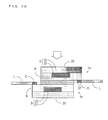
- Fig. 10 is a schematic view illustrating a method for measuring contact resistances of the FPC boards 1s in the inventive examples 1 to 12 and the comparative examples 1 and 2.
- a pair of FPC boards 1s in each of the inventive examples 1 to 12 and the comparative examples 1 and 2 was prepared.
- the pair of FPC boards 1s was arranged so that surfaces of cover layers 6 opposed each other while carbon paper CP was arranged between the cover layers 6 in the pair of FPC boards 1s.
- a resistance measuring device (ACmQ HITESTER manufactured by HIOKI E.E. CORPORATION) was connected to the cover layer 6 in each of the FPC board 1s via a connection terminal C and a connection line L.
- the pair of FPC board 1s was pressed against one surface and the other surface of the carbon paper CP at a pressure of 1 MPa.
- the resistance measuring device measured a resistance value between the connection terminals C in the pair of FPC board 1s as a contact resistance.
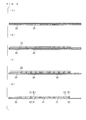
- Table 1 illustrates results of the thickness of the barrier layer 32, the presence or absence of corrosion of the conductor layer 31, and the contact resistance of the FPC board 1s.
- the barrier layer 32 As illustrated in Table 1, in the FPC board 1s s in the inventive example 1, as a result of measuring the thickness of the barrier layer 32, the barrier layer 32 having a thickness of 120 nm was formed to cover the main surface E1 and the side surface E3 of the conductor layer 31. As a result of immersing the FPC board 1s in the formic acid solution, the corrosion of the conductor layer 31 was not observed.
- the contact resistances of the FPC board 1s before and after the immersion in the formic acid solution were respectively 23 m ⁇ and 24 m ⁇ .
- the barrier layer 32 having a thickness of 120 nm was formed to cover the main surface E1 and the side surface E3 of the conductor layer 31.
- the corrosion of the conductor layer 31 was not observed.
- the contact resistances of the FPC board 1s before and after the immersion in the formic acid solution were respectively 19 m ⁇ and 23 m ⁇ .
- the barrier layer 32 having a thickness of 120 nm was formed to cover the main surface E1 and the side surface E3 of the conductor layer 31.
- the contact resistances of the FPC board 1s before and after the immersion in the formic acid solution were respectively 23 m ⁇ and 24 m ⁇ .
- the barrier layer 32 having a thickness of 120 nm was formed to cover the main surface E1 and the side surface E3 of the conductor layer 31.
- the contact resistances of the FPC board 1s before and after the immersion in the formic acid solution were respectively 20 m ⁇ and 22 m ⁇ .
- the barrier layer 32 having a thickness of 100 nm was formed to cover the main surface E1 and the side surface E3 of the conductor layer 31.
- the corrosion of the conductor layer 31 was not observed.
- the contact resistances of the FPC board 1s before and after the immersion in the formic acid solution were respectively 21 m ⁇ and 28 m ⁇ .
- the barrier layer 32 having a thickness of 30 nm was formed to cover the main surface E1 and the side surface E3 of the conductor layer 31.
- the contact resistances of the FPC board 1s before and after the immersion in the formic acid solution were respectively 22 m ⁇ and 24 m ⁇ .
- the barrier layer 32 having a thickness of 300 nm was formed to cover the main surface E1 and the side surface E3 of the conductor layer 31.
- the corrosion of the conductor layer 31 was not observed.
- the contact resistances of the FPC board 1s before and after the immersion in the formic acid solution were respectively 22 m ⁇ and 23 m ⁇ .
- the barrier layer 32 having a thickness of 150 nm was formed to cover the main surface E1 and the side surface E3 of the conductor layer 31.
- the contact resistances of the FPC board 1s before and after the immersion in the formic acid solution were respectively 20 m ⁇ and 22 m ⁇ .
- the barrier layer 32 having a thickness of 40 nm was formed to cover the main surface E1 and the side surface E3 of the conductor layer 31.
- the contact resistances of the FPC board 1s before and after the immersion in the formic acid solution were respectively 21 m ⁇ and 25 m ⁇ .
- the barrier layer 32 having a thickness of 350 nm was formed to cover the main surface E1 and the side surface E3 of the conductor layer 31.
- the corrosion of the conductor layer 31 was not observed.
- the contact resistances of the FPC board 1s before and after the immersion in the formic acid solution were respectively 22 m ⁇ and 23 m ⁇ .
- the barrier layer 32 having a thickness of 4 nm was formed to cover the main surface E1 and the side surface E3 of the conductor layer 31.
- the contact resistances of the FPC board 1s before and after the immersion in the formic acid solution were respectively 24 m ⁇ and 550 m ⁇ .
- the barrier layer 32 having a thickness of 510 nm was formed to cover the main surface E1 and the side surface E3 of the conductor layer 31.
- the corrosion of the conductor layer 31 was not observed.
- the contact resistances of the FPC board 1s before and after the immersion in the formic acid solution were respectively 24 m ⁇ and 600 m ⁇ .
- the barrier layer 32 was not formed in the conductor layer 31.
- the corrosion of the conductor layer 31 was observed.
- the contact resistances of the FPC board 1s before and after the immersion in the formic acid solution were respectively 20 m ⁇ and 1634 m ⁇ .
- the barrier layer 32 was not formed in the conductor layer 31.
- the corrosion of the conductor layer 31 was observed.
- the contact resistances of the FPC board 1s before and after the immersion in the formic acid solution were respectively 21 m ⁇ and 1715 m ⁇ .
- the barrier layer 32 was formed to cover the main surface E1 and the side surface E3 of the conductor layer 31 by applying the cover layer precursor 60 containing a heterocyclic compound on the main surface E1 and the side surface E3 of the conductor layer 31 and performing curing processing of the coating layer precursor 60 under a predetermined condition. From the result in the inventive example 8, it was confirmed that the barrier layer 32 was formed to cover the main surface E1 and the side surface E3 of the conductor layer 31 by applying a solution containing a heterocyclic compound was applied on the main surface E1 and the side surface E3 of the conductor layer 31 and performing curing processing of the solution under a predetermined condition.
Landscapes
- Engineering & Computer Science (AREA)
- Chemical & Material Sciences (AREA)
- Manufacturing & Machinery (AREA)
- Chemical Kinetics & Catalysis (AREA)
- Electrochemistry (AREA)
- Sustainable Energy (AREA)
- Sustainable Development (AREA)
- Life Sciences & Earth Sciences (AREA)
- General Chemical & Material Sciences (AREA)
- Microelectronics & Electronic Packaging (AREA)
- Health & Medical Sciences (AREA)
- Medicinal Chemistry (AREA)
- Polymers & Plastics (AREA)
- Organic Chemistry (AREA)
- Fuel Cell (AREA)
- Non-Metallic Protective Coatings For Printed Circuits (AREA)
- Compositions Of Macromolecular Compounds (AREA)
Applications Claiming Priority (1)
| Application Number | Priority Date | Filing Date | Title |
|---|---|---|---|
| JP2011014085A JP2012156309A (ja) | 2011-01-26 | 2011-01-26 | 配線回路基板およびその製造方法ならびに燃料電池 |
Publications (2)
| Publication Number | Publication Date |
|---|---|
| EP2482372A2 true EP2482372A2 (de) | 2012-08-01 |
| EP2482372A3 EP2482372A3 (de) | 2012-09-05 |
Family
ID=45065776
Family Applications (1)
| Application Number | Title | Priority Date | Filing Date |
|---|---|---|---|
| EP11190710A Withdrawn EP2482372A3 (de) | 2011-01-26 | 2011-11-25 | Leiterplatte und Verfahren zu ihrer Herstellung sowie Brennstoffzelle |
Country Status (6)
| Country | Link |
|---|---|
| US (1) | US20120189874A1 (de) |
| EP (1) | EP2482372A3 (de) |
| JP (1) | JP2012156309A (de) |
| KR (1) | KR20120086658A (de) |
| CN (1) | CN102625565A (de) |
| TW (1) | TWI526134B (de) |
Families Citing this family (1)
| Publication number | Priority date | Publication date | Assignee | Title |
|---|---|---|---|---|
| CN109219236B (zh) * | 2017-06-30 | 2021-11-02 | 宏启胜精密电子(秦皇岛)有限公司 | 透明柔性电路板及其制备方法 |
Citations (1)
| Publication number | Priority date | Publication date | Assignee | Title |
|---|---|---|---|---|
| JP2004200064A (ja) | 2002-12-19 | 2004-07-15 | Fujitsu Component Ltd | 燃料電池および燃料電池スタック |
Family Cites Families (12)
| Publication number | Priority date | Publication date | Assignee | Title |
|---|---|---|---|---|
| US4093768A (en) * | 1976-02-19 | 1978-06-06 | Freeman Chemical Corporation | Copper foil electrical laminate with reinforced plastics |
| US6344157B1 (en) * | 1999-02-12 | 2002-02-05 | National Starch And Chemical Investment Holding Corporation | Conductive and resistive materials with electrical stability for use in electronics devices |
| JP4309602B2 (ja) * | 2001-04-25 | 2009-08-05 | メック株式会社 | 銅または銅合金と樹脂との接着性を向上させる方法、ならびに積層体 |
| US7175929B2 (en) * | 2002-11-25 | 2007-02-13 | Fujitsu Component Limited | Fuel cell, method of manufacturing the same, and fuel cell stack including the same |
| JP3877717B2 (ja) * | 2003-09-30 | 2007-02-07 | 三洋電機株式会社 | 半導体装置およびその製造方法 |
| JP2007035995A (ja) * | 2005-07-28 | 2007-02-08 | Fujitsu Ltd | 銅表面処理液、積層体の製造方法および積層体 |
| EP2042580A4 (de) * | 2006-07-05 | 2009-12-09 | Henkel Ablestik Japan Ltd | Leitfähiger klebstoff |
| JP4886581B2 (ja) * | 2007-04-18 | 2012-02-29 | 日東電工株式会社 | 配線回路基板および燃料電池 |
| JP2008300238A (ja) * | 2007-05-31 | 2008-12-11 | Nitto Denko Corp | 配線回路基板および燃料電池 |
| JP2009094361A (ja) * | 2007-10-10 | 2009-04-30 | Nitto Denko Corp | Cof基板 |
| CN102396113B (zh) * | 2009-04-28 | 2014-09-24 | 日立化成株式会社 | 电路连接材料、使用该材料的膜状电路连接材料、电路部件的连接结构以及电路部件的连接方法 |
| JP5592808B2 (ja) * | 2010-09-15 | 2014-09-17 | 日東電工株式会社 | 配線回路基板 |
-
2011
- 2011-01-26 JP JP2011014085A patent/JP2012156309A/ja active Pending
- 2011-11-25 EP EP11190710A patent/EP2482372A3/de not_active Withdrawn
- 2011-12-02 TW TW100144411A patent/TWI526134B/zh not_active IP Right Cessation
- 2011-12-06 US US13/312,353 patent/US20120189874A1/en not_active Abandoned
-
2012
- 2012-01-10 KR KR1020120002896A patent/KR20120086658A/ko not_active Withdrawn
- 2012-01-16 CN CN2012100128843A patent/CN102625565A/zh active Pending
Patent Citations (1)
| Publication number | Priority date | Publication date | Assignee | Title |
|---|---|---|---|---|
| JP2004200064A (ja) | 2002-12-19 | 2004-07-15 | Fujitsu Component Ltd | 燃料電池および燃料電池スタック |
Also Published As
| Publication number | Publication date |
|---|---|
| TW201242465A (en) | 2012-10-16 |
| KR20120086658A (ko) | 2012-08-03 |
| JP2012156309A (ja) | 2012-08-16 |
| TWI526134B (zh) | 2016-03-11 |
| CN102625565A (zh) | 2012-08-01 |
| EP2482372A3 (de) | 2012-09-05 |
| US20120189874A1 (en) | 2012-07-26 |
Similar Documents
| Publication | Publication Date | Title |
|---|---|---|
| US20080298036A1 (en) | Printed circuit board and fuel cell | |
| TW201136007A (en) | Printed circuit board and fuel cell | |
| EP2388850A2 (de) | Leiterplatte, Brennstoffzelle und Verfahren zur Herstellung einer Leiterplatte | |
| JP5833003B2 (ja) | 可撓性回路基板およびその製造方法、ならびに該可撓性回路基板を用いた燃料電池 | |
| EP2431414A1 (de) | Pastenzusammensetzung und Leiterplatte | |
| EP2389051B1 (de) | Verfahren zur Herstellung einer Leiterplatte | |
| EP2482372A2 (de) | Leiterplatte und Verfahren zu ihrer Herstellung sowie Brennstoffzelle | |
| EP2482624A1 (de) | Pastenzusammensetzung und Druckleiterplatte | |
| KR20100024360A (ko) | 배선 회로 기판 및 연료 전지 | |
| US20110189508A1 (en) | Printed circuit board and fuel cell including the same | |
| JP7043731B2 (ja) | 銅張積層基板とその製造方法、並びに配線基板 | |
| JP2011108525A (ja) | 配線回路基板およびそれを備えた燃料電池 | |
| JP2011233693A (ja) | 配線回路基板および燃料電池 | |
| US20070186415A1 (en) | Anticorrosive bipolar fuel cell board and method for manufacturing the same | |
| JP2006210772A (ja) | フレキシブルプリント配線基板およびその製造方法、ならびに複合配線基板 |
Legal Events
| Date | Code | Title | Description |
|---|---|---|---|
| PUAI | Public reference made under article 153(3) epc to a published international application that has entered the european phase |
Free format text: ORIGINAL CODE: 0009012 |
|
| AK | Designated contracting states |
Kind code of ref document: A2 Designated state(s): AL AT BE BG CH CY CZ DE DK EE ES FI FR GB GR HR HU IE IS IT LI LT LU LV MC MK MT NL NO PL PT RO RS SE SI SK SM TR |
|
| AX | Request for extension of the european patent |
Extension state: BA ME |
|
| PUAL | Search report despatched |
Free format text: ORIGINAL CODE: 0009013 |
|
| AK | Designated contracting states |
Kind code of ref document: A3 Designated state(s): AL AT BE BG CH CY CZ DE DK EE ES FI FR GB GR HR HU IE IS IT LI LT LU LV MC MK MT NL NO PL PT RO RS SE SI SK SM TR |
|
| AX | Request for extension of the european patent |
Extension state: BA ME |
|
| RIC1 | Information provided on ipc code assigned before grant |
Ipc: H05K 1/16 20060101ALI20120731BHEP Ipc: H01M 8/02 20060101AFI20120731BHEP Ipc: C08K 5/3472 20060101ALI20120731BHEP Ipc: H01M 8/10 20060101ALI20120731BHEP |
|
| 17P | Request for examination filed |
Effective date: 20130122 |
|
| STAA | Information on the status of an ep patent application or granted ep patent |
Free format text: STATUS: THE APPLICATION HAS BEEN WITHDRAWN |
|
| 18W | Application withdrawn |
Effective date: 20160405 |