EP2481703B1 - Sensorschutz - Google Patents
Sensorschutz Download PDFInfo
- Publication number
- EP2481703B1 EP2481703B1 EP11000640.0A EP11000640A EP2481703B1 EP 2481703 B1 EP2481703 B1 EP 2481703B1 EP 11000640 A EP11000640 A EP 11000640A EP 2481703 B1 EP2481703 B1 EP 2481703B1
- Authority
- EP
- European Patent Office
- Prior art keywords
- substrate
- spacer
- front side
- sensor chip
- sensing element
- Prior art date
- Legal status (The legal status is an assumption and is not a legal conclusion. Google has not performed a legal analysis and makes no representation as to the accuracy of the status listed.)
- Active
Links
- 239000000758 substrate Substances 0.000 claims description 133
- 125000006850 spacer group Chemical group 0.000 claims description 69
- 238000004519 manufacturing process Methods 0.000 claims description 27
- 238000000034 method Methods 0.000 claims description 26
- 239000004020 conductor Substances 0.000 claims description 20
- 239000004065 semiconductor Substances 0.000 claims description 19
- 238000005530 etching Methods 0.000 claims description 16
- 239000002184 metal Substances 0.000 claims description 12
- 239000000919 ceramic Substances 0.000 claims description 9
- 239000011521 glass Substances 0.000 claims description 8
- 239000007788 liquid Substances 0.000 claims description 3
- 239000000126 substance Substances 0.000 claims description 3
- 239000003989 dielectric material Substances 0.000 claims description 2
- 235000012431 wafers Nutrition 0.000 description 37
- 229910052710 silicon Inorganic materials 0.000 description 25
- 239000010703 silicon Substances 0.000 description 25
- 238000012545 processing Methods 0.000 description 17
- 239000011248 coating agent Substances 0.000 description 15
- 238000000576 coating method Methods 0.000 description 15
- XUIMIQQOPSSXEZ-UHFFFAOYSA-N Silicon Chemical compound [Si] XUIMIQQOPSSXEZ-UHFFFAOYSA-N 0.000 description 13
- 239000012528 membrane Substances 0.000 description 9
- VYPSYNLAJGMNEJ-UHFFFAOYSA-N Silicium dioxide Chemical compound O=[Si]=O VYPSYNLAJGMNEJ-UHFFFAOYSA-N 0.000 description 7
- 239000000463 material Substances 0.000 description 7
- 229920000642 polymer Polymers 0.000 description 7
- 229910052814 silicon oxide Inorganic materials 0.000 description 7
- 229910000679 solder Inorganic materials 0.000 description 7
- 238000012360 testing method Methods 0.000 description 4
- 230000009286 beneficial effect Effects 0.000 description 3
- 238000004891 communication Methods 0.000 description 3
- 238000000708 deep reactive-ion etching Methods 0.000 description 3
- 238000000151 deposition Methods 0.000 description 3
- 238000000465 moulding Methods 0.000 description 3
- 238000011282 treatment Methods 0.000 description 3
- 230000003321 amplification Effects 0.000 description 2
- 238000005266 casting Methods 0.000 description 2
- 230000008021 deposition Effects 0.000 description 2
- 238000011156 evaluation Methods 0.000 description 2
- 230000000763 evoking effect Effects 0.000 description 2
- 239000012530 fluid Substances 0.000 description 2
- 239000011888 foil Substances 0.000 description 2
- 238000005259 measurement Methods 0.000 description 2
- 238000003199 nucleic acid amplification method Methods 0.000 description 2
- 238000004806 packaging method and process Methods 0.000 description 2
- 230000001133 acceleration Effects 0.000 description 1
- 239000000853 adhesive Substances 0.000 description 1
- 230000001070 adhesive effect Effects 0.000 description 1
- 230000005540 biological transmission Effects 0.000 description 1
- 239000006227 byproduct Substances 0.000 description 1
- 239000003990 capacitor Substances 0.000 description 1
- 238000005520 cutting process Methods 0.000 description 1
- 230000001419 dependent effect Effects 0.000 description 1
- 238000005516 engineering process Methods 0.000 description 1
- 238000000227 grinding Methods 0.000 description 1
- 238000010438 heat treatment Methods 0.000 description 1
- 239000012212 insulator Substances 0.000 description 1
- 238000005304 joining Methods 0.000 description 1
- 239000000203 mixture Substances 0.000 description 1
- 150000004767 nitrides Chemical class 0.000 description 1
- 238000012858 packaging process Methods 0.000 description 1
- 230000002093 peripheral effect Effects 0.000 description 1
- 230000001681 protective effect Effects 0.000 description 1
- 230000001012 protector Effects 0.000 description 1
- 239000000523 sample Substances 0.000 description 1
- 230000035945 sensitivity Effects 0.000 description 1
- 239000003351 stiffener Substances 0.000 description 1
- 230000002195 synergetic effect Effects 0.000 description 1
Images


Classifications
-
- G—PHYSICS
- G01—MEASURING; TESTING
- G01R—MEASURING ELECTRIC VARIABLES; MEASURING MAGNETIC VARIABLES
- G01R31/00—Arrangements for testing electric properties; Arrangements for locating electric faults; Arrangements for electrical testing characterised by what is being tested not provided for elsewhere
- G01R31/28—Testing of electronic circuits, e.g. by signal tracer
- G01R31/282—Testing of electronic circuits specially adapted for particular applications not provided for elsewhere
- G01R31/2831—Testing of materials or semi-finished products, e.g. semiconductor wafers or substrates
-
- B—PERFORMING OPERATIONS; TRANSPORTING
- B81—MICROSTRUCTURAL TECHNOLOGY
- B81C—PROCESSES OR APPARATUS SPECIALLY ADAPTED FOR THE MANUFACTURE OR TREATMENT OF MICROSTRUCTURAL DEVICES OR SYSTEMS
- B81C1/00—Manufacture or treatment of devices or systems in or on a substrate
- B81C1/00015—Manufacture or treatment of devices or systems in or on a substrate for manufacturing microsystems
- B81C1/00261—Processes for packaging MEMS devices
- B81C1/00333—Aspects relating to packaging of MEMS devices, not covered by groups B81C1/00269 - B81C1/00325
-
- B—PERFORMING OPERATIONS; TRANSPORTING
- B81—MICROSTRUCTURAL TECHNOLOGY
- B81C—PROCESSES OR APPARATUS SPECIALLY ADAPTED FOR THE MANUFACTURE OR TREATMENT OF MICROSTRUCTURAL DEVICES OR SYSTEMS
- B81C1/00—Manufacture or treatment of devices or systems in or on a substrate
-
- B—PERFORMING OPERATIONS; TRANSPORTING
- B81—MICROSTRUCTURAL TECHNOLOGY
- B81B—MICROSTRUCTURAL DEVICES OR SYSTEMS, e.g. MICROMECHANICAL DEVICES
- B81B7/00—Microstructural systems; Auxiliary parts of microstructural devices or systems
-
- G—PHYSICS
- G01—MEASURING; TESTING
- G01N—INVESTIGATING OR ANALYSING MATERIALS BY DETERMINING THEIR CHEMICAL OR PHYSICAL PROPERTIES
- G01N33/00—Investigating or analysing materials by specific methods not covered by groups G01N1/00 - G01N31/00
-
- H—ELECTRICITY
- H01—ELECTRIC ELEMENTS
- H01L—SEMICONDUCTOR DEVICES NOT COVERED BY CLASS H10
- H01L24/00—Arrangements for connecting or disconnecting semiconductor or solid-state bodies; Methods or apparatus related thereto
- H01L24/93—Batch processes
- H01L24/94—Batch processes at wafer-level, i.e. with connecting carried out on a wafer comprising a plurality of undiced individual devices
-
- G—PHYSICS
- G01—MEASURING; TESTING
- G01N—INVESTIGATING OR ANALYSING MATERIALS BY DETERMINING THEIR CHEMICAL OR PHYSICAL PROPERTIES
- G01N33/00—Investigating or analysing materials by specific methods not covered by groups G01N1/00 - G01N31/00
- G01N33/0004—Gaseous mixtures, e.g. polluted air
- G01N33/0009—General constructional details of gas analysers, e.g. portable test equipment
- G01N33/0027—General constructional details of gas analysers, e.g. portable test equipment concerning the detector
-
- G—PHYSICS
- G09—EDUCATION; CRYPTOGRAPHY; DISPLAY; ADVERTISING; SEALS
- G09G—ARRANGEMENTS OR CIRCUITS FOR CONTROL OF INDICATING DEVICES USING STATIC MEANS TO PRESENT VARIABLE INFORMATION
- G09G1/00—Control arrangements or circuits, of interest only in connection with cathode-ray tube indicators; General aspects or details, e.g. selection emphasis on particular characters, dashed line or dotted line generation; Preprocessing of data
-
- H—ELECTRICITY
- H01—ELECTRIC ELEMENTS
- H01L—SEMICONDUCTOR DEVICES NOT COVERED BY CLASS H10
- H01L21/00—Processes or apparatus adapted for the manufacture or treatment of semiconductor or solid state devices or of parts thereof
-
- H—ELECTRICITY
- H01—ELECTRIC ELEMENTS
- H01L—SEMICONDUCTOR DEVICES NOT COVERED BY CLASS H10
- H01L2221/00—Processes or apparatus adapted for the manufacture or treatment of semiconductor or solid state devices or of parts thereof covered by H01L21/00
-
- H—ELECTRICITY
- H01—ELECTRIC ELEMENTS
- H01L—SEMICONDUCTOR DEVICES NOT COVERED BY CLASS H10
- H01L2224/00—Indexing scheme for arrangements for connecting or disconnecting semiconductor or solid-state bodies and methods related thereto as covered by H01L24/00
- H01L2224/01—Means for bonding being attached to, or being formed on, the surface to be connected, e.g. chip-to-package, die-attach, "first-level" interconnects; Manufacturing methods related thereto
- H01L2224/10—Bump connectors; Manufacturing methods related thereto
- H01L2224/12—Structure, shape, material or disposition of the bump connectors prior to the connecting process
- H01L2224/13—Structure, shape, material or disposition of the bump connectors prior to the connecting process of an individual bump connector
Definitions
- the present invention relates to a sensor chip, the use of such sensor chip, and a method for manufacturing a sensor chip.
- sensors tend to be integrated on semiconductor substrates. This kind of manufacturing is beneficial in that the size of the sensors can significantly be reduced compared to discrete type sensors, and such sensors can be arranged next to electronic circuitry integrated on the same semiconductor substrate which circuitry may include functions acting on a signal delivered by the sensor such as amplification, evaluation, etc.
- An integrated chip comprising a sensor is called sensor chip in the following.
- the sensor and possibly electronic circuitry are arranged at a front side of a substrate.
- the circuitry may be formed by CMOS processing, and the building and/or arranging of a sensing element of the sensor on the front side may be implemented in a way compatible to CMOS processing.
- the sensor chip typically will be connected to circuitry residing on a different circuit board, such as a printed circuit board, for example.
- a preferred way for mounting a sensor chip to such circuit board is a technique called flip chip mounting in which the sensor chip is flipped such that its front side containing the sensing element and the circuitry faces the circuit board and is electrically connected to it.
- the electrical connection typically is achieved between contact pads arranged at the front side of the sensor chip and contact pads arranged on the circuit board and solder material in between.
- the sensing element faces the circuit board which may not be preferred for various reasons: In case the sensor shall detect a quantity of a measure in the environment of the sensor, such measure may not have sufficient access to the sensing element for the reason of its arrangement facing the circuit board. And even if there is sufficient access granted to the medium to be measured, it may not be appreciated that such medium also gets in touch with the circuit board. In case, for example, the medium to be measured is a gas, such gas may damage the circuitry on the circuit board.
- through-silicon vias may be applied.
- Such vias are arranged in the semiconductor substrate and represent vertical electrical connections between the front side of the substrate and its back side.
- a sensor chip with through-silicon vias can be mounted on the circuit board with its back side facing the circuit board and with its front side including the sensing element facing away from the circuit board.
- Contact pads arranged at the back side of the sensor chip allow electrically contacting the circuit board.
- a micro-electromechanical systems (MEMS) device having conductively filled vias.
- a MEMS component is formed on a substrate.
- the substrate has conductively filled vias extending therethrough.
- the MEMS component is electrically coupled to the conductively filled vias.
- the MEMS component is covered by a protective cap.
- An electrical interconnect is formed on a bottom surface of the substrate for transmission of electrical signals to the MEMS component, rather than using wirebonds.
- an electronic component package includes a package substrate portion constructed by a silicon substrate in which a through hole is provided, an insulating layer formed on both surface sides of the silicon substrate and an inner surface of the through hole, and a through electrode filled in the through hole, and a frame portion provided upright on a peripheral portion of the package substrate portion to constitute a cavity on the silicon substrate, wherein an upper surface of the through electrode in the cavity is planarized such that a height of the through electrode is set equal to a height of the insulating layer.
- the frame portion is joined to the package substrate portion by the low-temperature joining utilizing the plasma process after the through electrode is planarized.
- a vacuum sealed package for a semiconductor chip such as a micro-electromechanical (MEM) chip
- the package includes a ceramic substrate and a lid that together define a cavity wherein the chip is mounted.
- the substrate includes a conductive (e.g., metal) interconnect pattern that extends, at least in part, vertically through the substrate. I/O terminals are provided on an external surface of the substrate.
- a vent hole at least partially lined with a metal coating, extends through the substrate into the cavity.
- a metal plug seals the vent hole. The vent hole is sealed by placing the package in a vacuum chamber, evacuating the chamber, and heating the chamber so as to cause a metal preform on the substrate to flow into the vent hole and form the plug.
- a microstructured component with microsensors or other active mircro component includes a substrate and at least one housing arranged on the substrate with one or more active microstructures situated on it.
- a MEMS device has at least one conductive path extending from the top facing side of its substrate (having MEMS structure) to the bottom side of the noted substrate.
- the at least one conductive path extends through the substrate as noted to electrically connect the bottom facing side with the MEMS structure.
- an acceleration sensor comprises a first substrate, a multilayer second substrate and a sensor portion.
- the multilayer second substrate is opposed to the first substrate.
- the multilayer second substrate is provided with an electrode drawing opening.
- the multilayer second substrate consists of a plurality of layers.
- the sensor portion (a movable mass body and a fixed electrode) is provided in a sealed cavity portion which is formed between the first substrate and the multilayer second substrate which are opposed to each other.
- a micro-electromechanical-acoustic transducer assembly has a first die integrating a MEMS sensing structure having a membrane, which has a first surface in fluid communication with a front chamber and a second surface, opposite to the first surface, in fluid communication with a back chamber of the micro-electromechanical-acoustic transducer.
- the membrane is able to undergo a deformation as a function of incident acoustic-pressure waves, and faces a rigid electrode so as to form a variable-capacitance capacitor.
- a second die is provided, integrating an electronic reading circuit operatively coupled to the MEMS sensing structure and supplying an electrical output signal as a function of the capacitive variation.
- a package is provided, housing the first die and the second die and having a base substrate with electrical contacts towards the outside world.
- the first and second dice are set stacked in the package and directly connected together mechanically and electrically.
- the package delimits at least one between the front and back chambers.
- US 2005/186703 A1 discloses a method for packaging semiconductor chips and a corresponding semiconductor chip system.
- the method includes making available a semiconductor chip having a diaphragm region; providing a cap over the diaphragm region, while leaving the diaphragm region open; mounting the semiconductor chip on a support frame; and providing a molded housing around the semiconductor chip and at least a partial region of the support frame for packaging the semiconductor chip.
- the problem to be solved by the present invention is therefore to provide a sensor chip for which the handling during processing is facilitated.
- the sensor chip comprises a substrate with a front side and a back side.
- a sensing element and conductors are arranged at the front side, and contact pads are arranged at the back side. Vias extending through the substrate between the front side and the back side are provided for electrically connecting the conductors to the contact pads.
- a spacer is arranged at the front side.
- a substrate In processing a sensor chip, a substrate is provided with a front side and a back side, and a sensing element is arranged at the front side as is a spacer. Holes are etched into the substrate, and the holes are filled with a conducting material for building vias extending through the substrate between the front side and the back side.
- the spacer is arranged for protecting the sensing element during manufacturing. There are various steps in the manufacturing process where it is preferred to deposit the sensor chip with its front side onto some support. This may be owed to a need for applying manufacturing steps from the back side of the substrate or to a need for electrically contacting the contact pads arranged at the back side of the substrate. In such scenarios, the sensor chip can now be flipped and be deposited onto the support by means of its spacer, such that the spacer faces and sits on the support. As a result, the sensing element is protected and does not need to get in touch with any support during which contact the sensing element may become damaged or destroyed.
- the spacer acts as a protection element being arranged at the front side of the substrate and may protect not only the sensing element but also other structures such as integrated circuitry arranged at the front side of the substrate.
- FIGs 1a to 1g schematically illustrate different states of a sensor chip, each in a longitudinal cut, during its manufacture according to an embodiment of the present invention.
- the resulting sensor chip is shown according to an embodiment of the present invention.
- a schematic substrate 1 comprising a front side 11 and opposite to the front side 11 a back side 12.
- a height/depth/vertical extension/thickness of the substrate 1 is denoted by d1.
- the thickness d1 of the substrate 1 is between 500 ⁇ m and 800 ⁇ m which are a common standard thicknesses of wafers.
- a non visible surface of the substrate 1 extends into the plane of projection, which surface, also known as chip surface, is defined by a length x1 of the substrate 1 and a non-visible width y1.
- the substrate 1 advantageously is a semiconductor substrate, and preferably is a silicon substrate.
- the substrate 1 also may also be embodied as a ceramic, glass, polymer or other dielectric substrate.
- conductors 13 are applied to the first side 11 of the substrate 1, for example, by depositing metal paths where needed.
- the semiconductor substrate 1 is structured and processed by known processes such as CMOS processes in order to build conductors and other circuitry such as evaluation or amplification circuitry subject to the application and the scope of functionality of the sensor chip.
- CMOS processes in order to build conductors and other circuitry such as evaluation or amplification circuitry subject to the application and the scope of functionality of the sensor chip.
- circuitry may be integrated at the front side 11 of the substrate 1 where needed.
- an element when an element is to be arranged at the front side 11 of the substrate 1, such arrangement shall encompass a deposition of such element onto the surface of the substrate 1, it also shall encompass a deposition of such element onto other layers deposited on the surface of the substrate such that the element not necessarily touches the substrate 1 itself, and it shall also encompass elements/structures which are integrated into in the substrate close to the surface by means of, for example, the above mentioned semiconductor processing and as such are buried below other layers. Still such elements are arranged at the front side 11 in that they are not arranged at the back side or at lateral sides of the substrate 1.
- a sensing element 2 supporting the measurement is deposited on the substrate 1 at its front side 11.
- the sensing element 2 may be deposited on or buried into the substrate 1.
- the sensing element 2 may advantageously be formed by means of the same underlying processing steps as the circuitry is.
- a spacer 3 is arranged at the front side 11 of the substrate 1.
- Arranging the spacer 3 at the substrate 1 generally may include one of the following, without limitation:
- the spacer 3 may be an element formed separate from the substrate 1 and may be glued, bonded or otherwise mechanically connected to the substrate 1.
- the spacer 3 may directly be built on the substrate 1 in form of layers deposited on the substrate 1.
- the spacer 3 may be formed by moulding or casting onto the substrate 1.
- the spacer 3 may exhibit a form surrounding the sensing element 2.
- the sensing element 2 preferably is not covered by the spacer 3 in order to allow access to the sensing element 2.
- the spacer 3 has a height h1, which is preferably above 100 ⁇ m, and preferably is between 150 and 250 ⁇ m.
- the spacer 3 may be embodied as a resist, in particular as a dry resist, for example SU-8. Alternatively, it may be formed by a cast in a moulding process in which an insert is used for forming an opening 31 in the cast above the sensing element 2.
- the spacer 3 may also be provided in form of another substrate, for example, a silicon-on-insulator, or other semiconducting layer arrangements.
- the spacer 3 may be made from one of a semiconductor, silicon, silicon and a silicon-oxide coating, silicon and a solderable coating, ceramic, ceramic and a silicon-oxide coating, ceramic and a solderable coating, glass, glass and a silicon-oxide coating, glass and a solderable coating, metal, metal and a solderable coating, dielectric material and a polymer.
- the spacer 3 may cover and protect at least part of circuitry, and in particular metal structures, integrated into the substrate 1, however, it is preferred that the spacer 3 does not cover the sensing element 2.
- the building of integrated structures may be finalized by applying a dielectric layer such as an oxide, a silicon oxide or a nitride layer to the substrate 1 which shall cover any metal structures such as connectors or pads on the front side 11 of the substrate 1.
- a dielectric layer such as an oxide, a silicon oxide or a nitride layer
- such dielectric layer may be omitted during manufacture of the sensor chip.
- vias reaching through the substrate are preferably processed in subsequent steps.
- Such vias are manufactured by first etching holes into the substrate and filling these holes with electrically conductive material. For the reason that a high aspect ratio needs to be achieved for these holes conventional etching techniques may not be applicable.
- Special etching techniques such as anisotropic etching, which includes, for example deep reactive-ion etching (DRIE), may be applied for etching holes with such high aspect ratio.
- DRIE deep reactive-ion etching
- a diameter of the etched hole may strongly depend on its depth which depth may be equivalent to the thickness of the substrate. Approximately, the diameter evoked may be half of the depth of the hole.
- Silicon wafers from which the substrate for integrated circuits is formed typically exhibit a thickness of several hundred micrometers ⁇ m, for example 780 ⁇ m. Given this thickness, the diameter of a hole etched through the entire substrate for building a through-silicon via is about 390 ⁇ m.
- sensing elements may only cover small areas of a semiconductor chip such that even with additional circuitry included in such chip the overall chip surface may not exceed the order of few mm 2 . It becomes apparent that a couple of silicon through vias would claim a major part of the surface of such a chip. As a result, the chip surface would need to be extended only because of the vias representing the largest structures on the chip.
- the thickness d1 of the substrate 1 may be reduced in order to achieve holes with a diameter smaller than the diameter of holes etched into a substrate / wafer having a standard thickness.
- the substrate 1 is thinned, e.g. by grinding, to a reduced thickness d2 less than 300 ⁇ m, preferably less than 100 ⁇ m, and in a very preferred embodiment less than 50 ⁇ m.
- a reduced thickness d2 less than 300 ⁇ m, preferably less than 100 ⁇ m, and in a very preferred embodiment less than 50 ⁇ m.
- material from the substrate 1 is removed for reducing the thickness d1 of the substrate 1 down to the reduced thickness d2 in order to allow etching small size/diameter holes for realizing vias, a diameter of which holes depends on the thickness of the substrate 1.
- the diameter of such holes may be in the order of 75 ⁇ m.
- isotropic etching techniques may also be applied instead.
- multiple holes 14 for vias 15 can be etched into the substrate 1 after the substrate 1 has been thinned to the reduced thickness d2 without claiming the entire space on the chip surface.
- at least four through-silicon vias are formed, two for power, and two for communication.
- the spacer 3 may now be two fold: First, for thinning the substrate 1 the present sensor chip may need to be flipped and sit on a support. In such position, with the spacer 3 facing the support the sensing element 2 is protected by the spacer 3 in that the sensing element 2 does not get in touch with the support. And second, the spacer 3 may additionally act as a stiffener to the present sensor chip for the reason that as a result of the thinning step the thickness of the substrate 1 may be reduced to levels at which the substrate 1 no longer forms a rigid element but rather represents a thin flexible element. In order to compensate for the flexibility achieved as a by-product of the efforts of reducing the diameter of the through vias, the spacer 3 allows the sensor chip to form a rather rigid structure again and improves mechanical stability of the sensor chip and its handling.
- a state of the sensor chip after etching holes 14 into the substrate 1 is shown in Figure 1f .
- the holes 14 preferably are etched into the substrate 1 from its back side 12.
- the holes 14 are filled with conducting material such as Cu, polySi, Si, or others for implementing the various vias 15.
- a via 15 is understood as a conducting element reaching through the substrate 1.
- Conductors 17 provided at the back side 12 of the substrate 1 may connect the vias 15 to contact pads 16 provided elsewhere on the back side 12 of the substrate 1.
- the back side 12 of the substrate 1 may be understood as a redistribution layer which allows for finally arranging solder balls 18 on the contact pads 16 with a sufficient distance from each other, such as shown in Figure 1g .
- the conductors 17 of such redistribution layer may be formed on the substrate 1 at the very beginning of the process, for example, after the step illustrated in Figure 1b .
- some or all ends of the vias 15 at the back side 12 of the substrate 1 may form or especially be formed as contact pads 16.
- the sensor chip may be flipped and be seated on its spacer 3 which again protects the sensing element 2 and the other integrated structures during manufacturing. As a result, no other carrier is needed during building the through-silicon vias 15.
- the material used for the spacer 3 may show a high temperature stability and may be insensitive to treatments used during building the through-silicon vias 15 for the reason that the spacer 3 may be exposed to high temperatures and such treatments during building the through-silicon vias 15.
- the spacer 3 may comprise a membrane being arranged distant from the sensing element 2 for covering the opening 31.
- a membrane 51 is shown in Figure 2e .
- Such membrane 51 may be a polymer layer, be bonded to the spacer 3, and be provided as temporary protection during manufacturing, or, alternatively, as a permanent cover provided it allows sufficient access to the sensing element 2.
- the sensor chip according to Figure 1g represents a sensor chip according to an embodiment of the present invention.
- Such sensor chip can now be mounted to a circuit board with its back side 11 facing the circuit board.
- the sensor chip may be pressed with its solder bumps 18 against the circuit board, which in one embodiment may be a printed circuit board, in order to establish an electrical connection between the contact pads 16 of the sensor chip and contact pads of the circuit board.
- the solder bumps 18 may be hardened or otherwise treated such that a reliable electrical connection is established.
- the sensor chip may be mechanically fixed to the circuit board, for example by means of an adhesive at the back side 12 of the sensor chip, or by other means.
- the front side 11 of the sensor chip, and in particular its sensing element 2 faces the environment.
- the circuit board can be shielded from the measuring environment, for instance by means of an additional housing which may be sealed against the spacer 3.
- the spacer continues to provide protection to the sensing element 2 also during operation of the sensor chip.
- the sensing element 2 is sufficiently exposed to the measurement environment. There are no elements preventing access to the sensing element 2 as are when the sensor chip would be flip chip mounted to the circuit board. Any sensor signal from the sensing element or signals derived from such sensor signal now can be transmitted to the circuitry on the circuit board via the connectors 13 and the vias 15.
- the vias 15 represent an electrical connection between the front side 11 of the substrate 1 and its back side 12 and in particular may help to connect conductors 13 at the front side 11 of the substrate 1 with contact pads 16 on its back side.
- the sensor element 2 may be directly connected to the conductors 13 or via other circuitry.
- the vias 15 may be named through-silicon vias.
- the spacer 3 may be applied as protector during manufacturing of the vias 15. However, the spacer 3 may already perform a protecting function earlier in the process during a possible thinning of the substrate 1. In this context, it is beneficial that the spacer 3 is already attached to the substrate 1 prior to thinning the substrate 1 to its reduced thickness d2.
- the sensing element 2 may be arranged at the substrate 1 after the spacer 3 has been arranged at the substrate 1 provided that the technology for arranging the sensing element 2 is not prevented by the already arranged spacer 3.
- the spacer 3 may be arranged at the substrate 1 only for processing steps such as testing the sensor chip as will be explained in more detail with respect to Figure 2 .
- the vias 15 may be built first, and the circuitry/conductors 13 and the sensing element 2 may also be formed in a later step.
- the circuitry and the sensitive element 2 are integrated into the substrate 1 at the very beginning according to Figures 1a to 1c .
- the thickness d1 of the substrate 1 is reduced, for example by means of thinning its back side 12 according to Figure 1e , however, without the spacer 3 already being applied.
- the through-silicon vias 15 are built according to Figures 1f and 1g , again without the spacer 3 being applied to the substrate 1. After having formed the through-silicon vias 15 in the substrate 1, the spacer 3 is arranged according to Figure 1d , and solder bumps 18 are attached to the contact pads 16 such that a sensor chip according to Figure 1g is produced.
- Such processing is advantageous if the material used for the spacer 3 may show only low temperature stability and/or sensitivity to treatments used during forming the through-silicon vias 15. However, it may be preferred that during the processing of the through-silicon vias 15 a carrier may be applied for supporting the thinned substrate 1 and protecting it from being damaged.
- FIG. 2a - 2l schematically show different states of sensor chip processing on wafer scale, in a longitudinal cut each, according to an embodiment of the present invention.
- a resulting sensor chip arranged on a circuit board is illustrated according to an embodiment of the present invention.
- an entire wafer 4 is provided which wafer 4 constitutes a substrate for multiple sensor chips to be built from.
- the sensor chips are separated from each other into individual elements at the very end of the manufacturing process, as will be explained later.
- the wafer 4 forms a common substrate for all the sensor chips to be built.
- the initial manufacturing steps are the same as illustrated in Figure 1 .
- the wafer 4 is provided with a front side 11, a back side 12, and a height/depth/vertical extension/thickness d1.
- Circuitry including conductors 13 and possibly other electronic components are integrated into the wafer 4 by means of CMOS processing, see Figure 2b , now for multiple sensor chips to be built.
- an array of sensing elements 2 is formed on or in the wafer 4.
- sensing elements 2 can be built by the same processing steps the circuitry is built from, and, for example, such sensing elements 2 may include polymer layers receptive to humidity in the present example such that the sensor chip represents a humidity sensor for measuring a relative humidity of the environment.
- the sensing elements 2 may alternatively be deposited on the wafer 4 in form of a film covering the entire wafer and be structured to finally form the individual sensing elements 2 as shown in Figure 2c .
- the spacers are applied to the substrate 1 subsequently.
- Applying/arranging the spacers 3 to/at the wafer 4 may include providing multiple spacers 3 in form of a plate 5.
- a shown in Figure 2d such plate 5 may be a plate 5 of a dry resist, for example, of other suitable material where openings 31 for accessing the sensing elements 2 are already prefabricated, or where subsequent to applying the plate 2 to the front side 11 of the wafer 4 such openings 31 are fabricated.
- it may be beneficial that the entire plate 5 has a length and width equivalent to the length and width of the wafer 4.
- the plate 5 specifically may be made from one of silicon, silicon and a silicon-oxide coating, silicon and a solderable coating, ceramic, ceramic and a silicon-oxide coating, ceramic and a solderable coating, glass, glass and a silicon-oxide coating, glass and a solderable coating, metal, metal and a solderable coating, and a polymer.
- applying/arranging the spacers 3 to/at the wafer 4 may include building multiple spacers 3 in form of layers deposited on the wafer 4.
- applying/arranging the spacers 3 to/at the wafer 4 may include building multiple spacers 3 by moulding or casting material onto the wafer 4.
- a membrane layer 51 is deposited on the spacer plate 5 / the spacers 3, for example by bonding, and forms part of the final spacers 3.
- the membrane layer 51 which may be embodied as a polymer layer, covers the openings 31, protects the sensing elements 2, is arranged distant from the sensing elements 2, and provides sufficient access for the medium to be measured.
- the holes 14 are etched for all the sensor chips, advantageously by deep reactive-ion etching. For this reason, the wafer arrangement is flipped and sits by means of its membrane layer 51 on a support not shown.
- all the holes 14 are filled with conductive material in order to build vias 15 reaching through the entire reduced thickness d2 of the wafer 4 in order to connect the conductors 13 of each sensor chip to its contact pads 16 on the back side 12, again, which contact pads 16 may be arranged offset from the associated via 15 as shown in Figure 2g , or may be arranged in a line the associated vias 15 at the backside 12 of the wafer 4, or may be arranged in any mix of a contact pads arrangement.
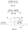
- the wafer arrangement In a subsequent step of processing the sensor chips, the wafer arrangement remains in its flipped state and is seated onto a chuck 6 with its membrane layer 51 facing the chuck 6 for the purpose of testing the sensor chips, see Figure 2h .
- electrical connections are established to the contact pads 16 now being easily accessible.
- a probe head 7 comprising electrodes 71 is arranged on top of the back side 12 of the wafer 4 and the electrodes 71 are brought into contact with the contact pads 16.
- test routines may be executed, wherein the sensing elements 2 are protected by the spacers which avoid the sensing elements 2 being in direct contact with the chuck 6.
- the wafer arrangement may be exposed to a medium evoking sensor responses that can be measured by means of the electrodes 71.
- a medium evoking sensor responses that can be measured by means of the electrodes 71.
- humid air may be supplied to the sensing elements 2 on the wafer 4.
- such medium advantageously is guided through openings in the chuck 6 - which are not explicitly shown in Figure 2h - for accessing the sensing elements 2 facing the chuck 6.
- the wafer 4 may be cut, for example along the dotted line, in order to separate the sensor chips from each other.
- the resulting individual sensor chips may be arranged on a foil 8, and possibly glued thereto for transporting purposes only.
- solder bumps may be applied to some or all the contact pads 16 on the back side 12 of the wafer 4 in order to prepare a mounting of the individual sensor chips to their destinations such as circuit boards.
- Such foil 8 with multiple sensor chips thereon may be supplied to an automatic assembly 9 as schematically illustrated in Figure 2l .
- a picker 91 picks an individual sensor chip at its spacer 3 and places such sensor chip onto its final destination which in the present example is a circuit board 10.
- the sensing element 2 as well as the entire sensor chip is protected by means of the spacer 3 which acts as a preferred contact surface for the picker 91.
- the sensor chip is mounted with its back side onto the circuit board 10 whereas its front side including the sensing element 2 and the spacer 3 are directed away from the circuit board 10.
- the sensor chip is used as one of a humidity sensor, a liquid flow sensor, a gas flow sensor, a pressure sensor, an infrared sensor and a chemical sensor. Corresponding sensing elements are provided for each of the applications.
Landscapes
- Engineering & Computer Science (AREA)
- Microelectronics & Electronic Packaging (AREA)
- Manufacturing & Machinery (AREA)
- Computer Hardware Design (AREA)
- Physics & Mathematics (AREA)
- General Physics & Mathematics (AREA)
- Power Engineering (AREA)
- Chemical & Material Sciences (AREA)
- Life Sciences & Earth Sciences (AREA)
- Health & Medical Sciences (AREA)
- General Engineering & Computer Science (AREA)
- General Health & Medical Sciences (AREA)
- Food Science & Technology (AREA)
- Immunology (AREA)
- Pathology (AREA)
- Medicinal Chemistry (AREA)
- Biochemistry (AREA)
- Analytical Chemistry (AREA)
- Testing Or Measuring Of Semiconductors Or The Like (AREA)
- Pressure Sensors (AREA)
- Solid State Image Pick-Up Elements (AREA)
- Measuring Fluid Pressure (AREA)
Claims (9)
- Verfahren zur Herstellung eines Sensorchips, umfassend die folgenden Schritte
Bereitstellen eines Halbleitersubstrats (1) mit einer Vorderseite (11) und einer Rückseite (12) und einer integrierten Schaltung, die auf der Vorderseite integriert ist,
Anordnen eines Sensorelements (2) an der Vorderseite (11), wobei das Sensorelement (2) geeignet ist, entweder Feuchtigkeit, Flüssigkeitsstrom, Gasstrom, Druck oder Chemikalien zu erfassen,
Anordnen eines Abstandhalters (3) an der Vorderseite (11),
Ätzen von Löchern (14) in das Substrat (1), und
Füllen der Löcher (14) mit einem leitenden Material zum Erstellen von Durchkontaktierungen (15), die sich durch das Substrat (1) zwischen der Vorderseite (11) und der Rückseite (12) erstrecken,
wobei der Abstandshalter (3) vor dem Ätzen der Löcher (14) an der Vorderseite (11) angeordnet wird, und
wobei sich der Abstandshalter (3) um das Sensorelement (2) herum erstreckt, mindestens einen Teil der integrierten Schaltung abdeckt und wobei das Sensorelement (2) der Umgebung zugewandt ist. - Verfahren nach Anspruch 1, wobei die Löcher (14) durch anisotropes Ätzen von der Rückseite (12) des Substrats (1) her geätzt werden.
- Verfahren nach Anspruch 1 oder Anspruch 2, wobei der Sensorchip auf einem Chuck (6) angeordnet ist, wobei der Abstandshalter (3) dem Chuck (6) zugewandt ist, um Kontaktpads (16), die auf der Rückseite (12) angeordnet sind, mit Elektroden (71) elektrisch zu kontaktieren.
- Verfahren nach Anspruch 3, bei dem der Sensorchip getestet wird, während er auf dem Chuck (6) angeordnet ist.
- Verfahren nach einem der vorhergehenden Ansprüche, bei dem ein Picker (91) einer automatischen Baugruppe (9) mit dem Abstandshalter (3) des Sensorchips in Eingriff kommt, um den Sensorchip auf einer Leiterplatte (10) zu platzieren.
- Verfahren nach einem der vorhergehenden Ansprüche,
wobei das Substrat (1) in Form eines Wafers (4) zum Herstellen mehrerer Sensorchips bereitgestellt wird, und
wobei Sensorelemente (2) und Leiter (13) für mehrere Sensorchips an der Vorderseite (11) des Wafers (4) angeordnet sind,
wobei mehrere Abstandshalter (3) für mehrere Sensorchips an der Vorderseite (11) des Wafers (4) angeordnet sind,
wobei der Schritt des Ätzens von Löchern (14) durch den Wafer (4) und des Füllens der Löcher (14) zum Aufbau von Durchkontaktierungen (15) für mehrere Sensorchips vor oder nach dem Anordnen der Abstandshalter (3) auf dem Wafer (4) erfolgt, und
wobei die vorhergehenden vier Schritte vor dem Trennen des Wafers (4) in mehrere Sensorchips durchgeführt werden. - Sensorchip, hergestellt nach dem Verfahren nach Anspruch 1, umfassend
ein Halbleitersubstrat (1) mit einer Vorderseite (11) und einer Rückseite (12),
einem Sensorelement (2) und Leitern (13), die an der Vorderseite (11) angeordnet sind, wobei das Sensorelement (2) der Umgebung zugewandt ist,
Kontaktpads (16), die auf der Rückseite (12) angeordnet sind,
Durchkontaktierungen (15), die sich durch das Substrat (1) zwischen der Vorderseite (11) und der Rückseite (12) erstrecken, um die Leiter (13) elektrisch mit den Kontaktpads (16) zu verbinden, und
einen an der Vorderseite (11) angeordneten Abstandshalter (3) zum Schutz des Sensorelements (2),
eine integrierte Schaltung, die an der Vorderseite (11) des Substrats (1) angeordnet ist, wobei mindestens ein Teil der integrierten Schaltung durch den Abstandshalter (3) abgedeckt ist,
wobei sich der Abstandshalter (3) um das Sensorelement (2) herum erstreckt, und
wobei das Sensorelement (2) so ausgelegt ist, dass es entweder Feuchtigkeit, Flüssigkeitsstrom, Gasstrom, Druck oder Chemikalien erfasst. - Sensorchip nach Anspruch 7, wobei der Abstandshalter (3) aus einem der folgenden Materialien hergestellt ist: Resist, Giessmaterial, Halbleiter, Keramik, Metall, dielektrisches Material, Glas.
- Sensorchip nach Anspruch 7 oder 8, wobei eine Dicke (h1) des Abstandshalters (3) mehr als 100 µm, und vorzugsweise zwischen 150 und 250 µm beträgt.
Priority Applications (9)
| Application Number | Priority Date | Filing Date | Title |
|---|---|---|---|
| EP11000640.0A EP2481703B1 (de) | 2011-01-27 | 2011-01-27 | Sensorschutz |
| PCT/CH2012/000019 WO2012100360A1 (en) | 2011-01-27 | 2012-01-26 | Sensor chip comprising a spacer for protecting the sensor element |
| KR1020137022245A KR101944128B1 (ko) | 2011-01-27 | 2012-01-26 | 센서 칩을 테스트하기 위한 장치를 포함하는 센서 칩을 제조하는 방법 |
| EP12702168.1A EP2668131A2 (de) | 2011-01-27 | 2012-01-26 | Verfahren zur herstellung eines sensorchips mit einem vorrichtung zum testen des chips |
| EP12702167.3A EP2668130A1 (de) | 2011-01-27 | 2012-01-26 | Sensorchip mit einem distanzstück zum schutz des sensorelementes |
| PCT/CH2012/000021 WO2012100362A1 (en) | 2011-01-27 | 2012-01-26 | Method for manufacturing a sensor chip |
| PCT/CH2012/000020 WO2012100361A2 (en) | 2011-01-27 | 2012-01-26 | Sensor protection |
| US13/981,651 US9366720B2 (en) | 2011-01-27 | 2012-01-26 | Sensor protection |
| JP2013550722A JP6038048B2 (ja) | 2011-01-27 | 2012-01-26 | センサチップを試験する装置を有するセンサチップの製造方法 |
Applications Claiming Priority (1)
| Application Number | Priority Date | Filing Date | Title |
|---|---|---|---|
| EP11000640.0A EP2481703B1 (de) | 2011-01-27 | 2011-01-27 | Sensorschutz |
Publications (2)
| Publication Number | Publication Date |
|---|---|
| EP2481703A1 EP2481703A1 (de) | 2012-08-01 |
| EP2481703B1 true EP2481703B1 (de) | 2020-07-01 |
Family
ID=44148336
Family Applications (3)
| Application Number | Title | Priority Date | Filing Date |
|---|---|---|---|
| EP11000640.0A Active EP2481703B1 (de) | 2011-01-27 | 2011-01-27 | Sensorschutz |
| EP12702168.1A Withdrawn EP2668131A2 (de) | 2011-01-27 | 2012-01-26 | Verfahren zur herstellung eines sensorchips mit einem vorrichtung zum testen des chips |
| EP12702167.3A Withdrawn EP2668130A1 (de) | 2011-01-27 | 2012-01-26 | Sensorchip mit einem distanzstück zum schutz des sensorelementes |
Family Applications After (2)
| Application Number | Title | Priority Date | Filing Date |
|---|---|---|---|
| EP12702168.1A Withdrawn EP2668131A2 (de) | 2011-01-27 | 2012-01-26 | Verfahren zur herstellung eines sensorchips mit einem vorrichtung zum testen des chips |
| EP12702167.3A Withdrawn EP2668130A1 (de) | 2011-01-27 | 2012-01-26 | Sensorchip mit einem distanzstück zum schutz des sensorelementes |
Country Status (5)
| Country | Link |
|---|---|
| US (1) | US9366720B2 (de) |
| EP (3) | EP2481703B1 (de) |
| JP (1) | JP6038048B2 (de) |
| KR (1) | KR101944128B1 (de) |
| WO (3) | WO2012100361A2 (de) |
Families Citing this family (24)
| Publication number | Priority date | Publication date | Assignee | Title |
|---|---|---|---|---|
| EP2731129A1 (de) * | 2012-11-07 | 2014-05-14 | ams AG | Gegossene Halbleitersensorvorrichtung und Verfahren zu ihrer Herstellung auf Waferebene |
| EP2762865A1 (de) * | 2013-01-31 | 2014-08-06 | Sensirion Holding AG | Chemische Sensor und Verfahren zur Herstellung solch eines chemischen Sensors |
| EP2762869B1 (de) | 2013-01-31 | 2016-11-16 | Sensirion AG | Integrierter chemischer Metalloxidsensor |
| EP2762880B1 (de) | 2013-01-31 | 2017-03-15 | Sensirion AG | Tragbare elektronische Vorrichtung mit Atemanalysator |
| EP2762882B1 (de) | 2013-01-31 | 2020-11-25 | Sensirion AG | Tragbare elektronische Vorrichtung mit Keton-Sensor |
| EP2762870A1 (de) * | 2013-01-31 | 2014-08-06 | Sensirion AG | Sensoranordnung und tragbare elektronische Vorrichtung mit solch einer Sensoranordnung |
| EP2763381B1 (de) | 2013-01-31 | 2017-04-05 | Sensirion AG | Tragbare elektronische Vorrichtung mit chemischem Sensor |
| EP2801819A1 (de) | 2013-05-08 | 2014-11-12 | Sensirion AG | Metalloxid-chemischer Sensor für tragbare Vorrichtung |
| EP2808675A1 (de) | 2013-05-31 | 2014-12-03 | Sensirion AG | Integrierter chemischer Metalloxidsensor |
| DE202013102632U1 (de) * | 2013-06-19 | 2013-12-20 | Sensirion Ag | Sensorbaustein |
| EP2816352B1 (de) | 2013-06-21 | 2016-12-28 | Sensirion AG | Konzentrationsmessungen mit einer mobilen Vorrichtung |
| EP2833127A1 (de) | 2013-07-30 | 2015-02-04 | Sensirion AG | Integrierte resistive Sensorarrayanordnung, wobei jeder Sensor eine sensitive Metalloxidschicht mit jeweils verschiedenen Längen zwischen den Elektroden enthält |
| EP2833128A1 (de) | 2013-07-30 | 2015-02-04 | Sensirion AG | Integrierter chemischer Metalloxidsensor |
| EP2871152B1 (de) | 2013-11-06 | 2017-05-24 | Sensirion AG | Sensorvorrichtung |
| EP2946722A1 (de) | 2014-05-20 | 2015-11-25 | Sensirion AG | Tragbare elektronische Vorrichtung zur Entnahme einer Atemprobe |
| EP3001186B1 (de) * | 2014-09-26 | 2018-06-06 | Sensirion AG | Sensorchip |
| WO2016088099A1 (en) * | 2014-12-05 | 2016-06-09 | Lfoundry S.R.L. | Cmos process for manufacturing an integrated gas sensor and corresponding cmos integrated gas sensor |
| EP3032227B1 (de) | 2014-12-08 | 2020-10-21 | Sensirion AG | Flusssensorpaket |
| US10642391B2 (en) * | 2015-06-19 | 2020-05-05 | Lg Electronics Inc. | Touch panel and display device |
| CN109791117B (zh) | 2016-09-21 | 2022-09-20 | 盛思锐股份公司 | 气体传感器 |
| JP6917843B2 (ja) * | 2016-10-13 | 2021-08-11 | 理研計器株式会社 | ガスセンサ |
| US20180196022A1 (en) * | 2017-01-12 | 2018-07-12 | Integrated Device Technology, Inc. | Gas sensor |
| KR20190035989A (ko) | 2017-09-25 | 2019-04-04 | (주)센텍코리아 | 가스 센서 패키지 |
| US10727216B1 (en) | 2019-05-10 | 2020-07-28 | Sandisk Technologies Llc | Method for removing a bulk substrate from a bonded assembly of wafers |
Citations (2)
| Publication number | Priority date | Publication date | Assignee | Title |
|---|---|---|---|---|
| US20050186703A1 (en) * | 2004-01-23 | 2005-08-25 | Kurt Weiblen | Method for packaging semiconductor chips and corresponding semiconductor chip system |
| EP2252077A1 (de) * | 2009-05-11 | 2010-11-17 | STMicroelectronics Srl | Anordnung eines kapazitiven mikroelektromechanischen Akustikwandlers und Verpackung dafür |
Family Cites Families (33)
| Publication number | Priority date | Publication date | Assignee | Title |
|---|---|---|---|---|
| JPS63110671A (ja) | 1986-10-28 | 1988-05-16 | Sumitomo Electric Ind Ltd | 半導体圧力センサの測定方法 |
| DE3772514D1 (de) | 1986-10-28 | 1991-10-02 | Sumitomo Electric Industries | Messverfahren fuer einen halbleiter-druckmessfuehler. |
| JPH0233567A (ja) | 1988-07-20 | 1990-02-02 | Matsushita Electric Ind Co Ltd | 温風暖房機 |
| US5001423A (en) | 1990-01-24 | 1991-03-19 | International Business Machines Corporation | Dry interface thermal chuck temperature control system for semiconductor wafer testing |
| DE4239132C2 (de) * | 1991-11-20 | 2002-06-06 | Denso Corp | Verfahren zum Fabrizieren eines integrierten Drucksensors |
| JPH0933567A (ja) * | 1995-07-21 | 1997-02-07 | Akebono Brake Ind Co Ltd | 半導体加速度センサのセンサチップ検査方法及び検査装置 |
| US5865938A (en) * | 1996-06-25 | 1999-02-02 | Xerox Corporation | Wafer chuck for inducing an electrical bias across wafer heterojunctions |
| US6189483B1 (en) * | 1997-05-29 | 2001-02-20 | Applied Materials, Inc. | Process kit |
| US6083344A (en) * | 1997-05-29 | 2000-07-04 | Applied Materials, Inc. | Multi-zone RF inductively coupled source configuration |
| US6690569B1 (en) | 1999-12-08 | 2004-02-10 | Sensirion A/G | Capacitive sensor |
| AU2001247195A1 (en) * | 2000-01-31 | 2001-08-07 | Board Of Regents, The University Of Texas System | Method and system for collecting and transmitting chemical information |
| US6384353B1 (en) * | 2000-02-01 | 2002-05-07 | Motorola, Inc. | Micro-electromechanical system device |
| US6479320B1 (en) * | 2000-02-02 | 2002-11-12 | Raytheon Company | Vacuum package fabrication of microelectromechanical system devices with integrated circuit components |
| US6528875B1 (en) * | 2001-04-20 | 2003-03-04 | Amkor Technology, Inc. | Vacuum sealed package for semiconductor chip |
| US6624003B1 (en) * | 2002-02-06 | 2003-09-23 | Teravicta Technologies, Inc. | Integrated MEMS device and package |
| US20050029221A1 (en) * | 2003-08-09 | 2005-02-10 | Taiwan Semiconductor Manufacturing Co., Ltd. | Deep trench etching using HDP chamber |
| JP2005109221A (ja) * | 2003-09-30 | 2005-04-21 | Toshiba Corp | ウェーハレベルパッケージ及びその製造方法 |
| US6936918B2 (en) * | 2003-12-15 | 2005-08-30 | Analog Devices, Inc. | MEMS device with conductive path through substrate |
| EP1628132B1 (de) * | 2004-08-17 | 2015-01-07 | Sensirion Holding AG | Verfahren und Vorrichtung zur Eichung von Sensoren |
| JP2006173557A (ja) * | 2004-11-22 | 2006-06-29 | Toshiba Corp | 中空型半導体装置とその製造方法 |
| JP2006226743A (ja) * | 2005-02-16 | 2006-08-31 | Mitsubishi Electric Corp | 加速度センサ |
| DE102005014427B4 (de) * | 2005-03-24 | 2008-05-15 | Infineon Technologies Ag | Verfahren zum Verkapseln eines Halbleiterbauelements |
| JP4889974B2 (ja) * | 2005-08-01 | 2012-03-07 | 新光電気工業株式会社 | 電子部品実装構造体及びその製造方法 |
| US20070190747A1 (en) * | 2006-01-23 | 2007-08-16 | Tessera Technologies Hungary Kft. | Wafer level packaging to lidded chips |
| US7936062B2 (en) * | 2006-01-23 | 2011-05-03 | Tessera Technologies Ireland Limited | Wafer level chip packaging |
| WO2008023824A1 (fr) * | 2006-08-25 | 2008-02-28 | Sanyo Electric Co., Ltd. | Dispositif à semi-conducteur et son procédé de fabrication |
| DE102008025599B4 (de) * | 2007-05-14 | 2013-02-21 | Fraunhofer-Gesellschaft zur Förderung der angewandten Forschung e.V. | Gehäuste aktive Mikrostrukturen mit Direktkontaktierung zu einem Substrat |
| JP5137059B2 (ja) * | 2007-06-20 | 2013-02-06 | 新光電気工業株式会社 | 電子部品用パッケージ及びその製造方法と電子部品装置 |
| US8390117B2 (en) * | 2007-12-11 | 2013-03-05 | Panasonic Corporation | Semiconductor device and method of manufacturing the same |
| US20090178751A1 (en) * | 2007-12-11 | 2009-07-16 | Micro Foundry Inc. | Integrated miniature microfluidics device factory and method for use |
| JP5247396B2 (ja) * | 2008-07-02 | 2013-07-24 | 日本化薬株式会社 | Mems用感光性樹脂組成物及びその硬化物 |
| EP2154713B1 (de) | 2008-08-11 | 2013-01-02 | Sensirion AG | Verfahren zur Herstellung einer Messvorrichtung mit einer Spannungsverminderungsschicht |
| JP5535492B2 (ja) * | 2009-02-12 | 2014-07-02 | ラピスセミコンダクタ株式会社 | 半導体集積回路の検査装置及び半導体集積回路の検査方法 |
-
2011
- 2011-01-27 EP EP11000640.0A patent/EP2481703B1/de active Active
-
2012
- 2012-01-26 WO PCT/CH2012/000020 patent/WO2012100361A2/en active Application Filing
- 2012-01-26 WO PCT/CH2012/000019 patent/WO2012100360A1/en active Application Filing
- 2012-01-26 JP JP2013550722A patent/JP6038048B2/ja active Active
- 2012-01-26 EP EP12702168.1A patent/EP2668131A2/de not_active Withdrawn
- 2012-01-26 EP EP12702167.3A patent/EP2668130A1/de not_active Withdrawn
- 2012-01-26 WO PCT/CH2012/000021 patent/WO2012100362A1/en active Application Filing
- 2012-01-26 US US13/981,651 patent/US9366720B2/en active Active
- 2012-01-26 KR KR1020137022245A patent/KR101944128B1/ko active IP Right Grant
Patent Citations (2)
| Publication number | Priority date | Publication date | Assignee | Title |
|---|---|---|---|---|
| US20050186703A1 (en) * | 2004-01-23 | 2005-08-25 | Kurt Weiblen | Method for packaging semiconductor chips and corresponding semiconductor chip system |
| EP2252077A1 (de) * | 2009-05-11 | 2010-11-17 | STMicroelectronics Srl | Anordnung eines kapazitiven mikroelektromechanischen Akustikwandlers und Verpackung dafür |
Also Published As
| Publication number | Publication date |
|---|---|
| JP2014508288A (ja) | 2014-04-03 |
| KR20140006908A (ko) | 2014-01-16 |
| EP2481703A1 (de) | 2012-08-01 |
| WO2012100361A3 (en) | 2012-11-15 |
| WO2012100360A1 (en) | 2012-08-02 |
| EP2668131A2 (de) | 2013-12-04 |
| WO2012100362A1 (en) | 2012-08-02 |
| KR101944128B1 (ko) | 2019-01-30 |
| JP6038048B2 (ja) | 2016-12-07 |
| US20140028340A1 (en) | 2014-01-30 |
| EP2668130A1 (de) | 2013-12-04 |
| US9366720B2 (en) | 2016-06-14 |
| WO2012100361A2 (en) | 2012-08-02 |
Similar Documents
| Publication | Publication Date | Title |
|---|---|---|
| EP2481703B1 (de) | Sensorschutz | |
| US10816422B2 (en) | Pressure sensor | |
| US9046546B2 (en) | Sensor device and related fabrication methods | |
| KR101332701B1 (ko) | 기준 커패시터를 포함하는 미소 전자기계 압력 센서 | |
| TWI598965B (zh) | 混合整合構件及其製造方法 | |
| US8215176B2 (en) | Pressure sensor for harsh media sensing and flexible packaging | |
| TWI619669B (zh) | 製造混合整合構件的方法,包含至少兩 mems 元件的混合整合構件 | |
| US9227841B2 (en) | Apparatus integrating microelectromechanical system device with circuit chip and methods for fabricating the same | |
| EP2871455B1 (de) | Drucksensor | |
| EP3001186B1 (de) | Sensorchip | |
| TW201400401A (zh) | 混合整合構件及其製造方法 | |
| WO2006101689A1 (en) | Wafer level capped sensor | |
| US20050054133A1 (en) | Wafer level capped sensor | |
| EP2482310B1 (de) | Durchkontaktierungen in einem Sensorchip | |
| KR20160088111A (ko) | 복합 센서와 이를 구비하는 패키지 및 그 제조 방법 | |
| CN110088037B (zh) | 半导体器件和用于形成半导体器件的方法 | |
| US20170057810A1 (en) | Strain Reduction and Sensing on Package Substrates | |
| EP2725334B1 (de) | Drucksensor mit einer Membrane und Herstellungsverfahren dafür | |
| EP3385218B1 (de) | Halbleiterbauelement mit umweltsensor | |
| EP3601957B1 (de) | Sensor package | |
| CN116281835A (zh) | 一种mems器件及其制备方法、电子装置 |
Legal Events
| Date | Code | Title | Description |
|---|---|---|---|
| PUAI | Public reference made under article 153(3) epc to a published international application that has entered the european phase |
Free format text: ORIGINAL CODE: 0009012 |
|
| AK | Designated contracting states |
Kind code of ref document: A1 Designated state(s): AL AT BE BG CH CY CZ DE DK EE ES FI FR GB GR HR HU IE IS IT LI LT LU LV MC MK MT NL NO PL PT RO RS SE SI SK SM TR |
|
| AX | Request for extension of the european patent |
Extension state: BA ME |
|
| 17P | Request for examination filed |
Effective date: 20130201 |
|
| 17Q | First examination report despatched |
Effective date: 20140905 |
|
| STAA | Information on the status of an ep patent application or granted ep patent |
Free format text: STATUS: EXAMINATION IS IN PROGRESS |
|
| GRAP | Despatch of communication of intention to grant a patent |
Free format text: ORIGINAL CODE: EPIDOSNIGR1 |
|
| STAA | Information on the status of an ep patent application or granted ep patent |
Free format text: STATUS: GRANT OF PATENT IS INTENDED |
|
| INTG | Intention to grant announced |
Effective date: 20200218 |
|
| GRAS | Grant fee paid |
Free format text: ORIGINAL CODE: EPIDOSNIGR3 |
|
| GRAA | (expected) grant |
Free format text: ORIGINAL CODE: 0009210 |
|
| STAA | Information on the status of an ep patent application or granted ep patent |
Free format text: STATUS: THE PATENT HAS BEEN GRANTED |
|
| AK | Designated contracting states |
Kind code of ref document: B1 Designated state(s): AL AT BE BG CH CY CZ DE DK EE ES FI FR GB GR HR HU IE IS IT LI LT LU LV MC MK MT NL NO PL PT RO RS SE SI SK SM TR |
|
| REG | Reference to a national code |
Ref country code: GB Ref legal event code: FG4D |
|
| REG | Reference to a national code |
Ref country code: AT Ref legal event code: REF Ref document number: 1286024 Country of ref document: AT Kind code of ref document: T Effective date: 20200715 Ref country code: CH Ref legal event code: EP |
|
| REG | Reference to a national code |
Ref country code: IE Ref legal event code: FG4D |
|
| REG | Reference to a national code |
Ref country code: DE Ref legal event code: R096 Ref document number: 602011067533 Country of ref document: DE |
|
| REG | Reference to a national code |
Ref country code: LT Ref legal event code: MG4D |
|
| PG25 | Lapsed in a contracting state [announced via postgrant information from national office to epo] |
Ref country code: BG Free format text: LAPSE BECAUSE OF FAILURE TO SUBMIT A TRANSLATION OF THE DESCRIPTION OR TO PAY THE FEE WITHIN THE PRESCRIBED TIME-LIMIT Effective date: 20201001 |
|
| REG | Reference to a national code |
Ref country code: NL Ref legal event code: MP Effective date: 20200701 |
|
| REG | Reference to a national code |
Ref country code: AT Ref legal event code: MK05 Ref document number: 1286024 Country of ref document: AT Kind code of ref document: T Effective date: 20200701 |
|
| PG25 | Lapsed in a contracting state [announced via postgrant information from national office to epo] |
Ref country code: HR Free format text: LAPSE BECAUSE OF FAILURE TO SUBMIT A TRANSLATION OF THE DESCRIPTION OR TO PAY THE FEE WITHIN THE PRESCRIBED TIME-LIMIT Effective date: 20200701 Ref country code: ES Free format text: LAPSE BECAUSE OF FAILURE TO SUBMIT A TRANSLATION OF THE DESCRIPTION OR TO PAY THE FEE WITHIN THE PRESCRIBED TIME-LIMIT Effective date: 20200701 Ref country code: SE Free format text: LAPSE BECAUSE OF FAILURE TO SUBMIT A TRANSLATION OF THE DESCRIPTION OR TO PAY THE FEE WITHIN THE PRESCRIBED TIME-LIMIT Effective date: 20200701 Ref country code: NO Free format text: LAPSE BECAUSE OF FAILURE TO SUBMIT A TRANSLATION OF THE DESCRIPTION OR TO PAY THE FEE WITHIN THE PRESCRIBED TIME-LIMIT Effective date: 20201001 Ref country code: GR Free format text: LAPSE BECAUSE OF FAILURE TO SUBMIT A TRANSLATION OF THE DESCRIPTION OR TO PAY THE FEE WITHIN THE PRESCRIBED TIME-LIMIT Effective date: 20201002 Ref country code: AT Free format text: LAPSE BECAUSE OF FAILURE TO SUBMIT A TRANSLATION OF THE DESCRIPTION OR TO PAY THE FEE WITHIN THE PRESCRIBED TIME-LIMIT Effective date: 20200701 Ref country code: PT Free format text: LAPSE BECAUSE OF FAILURE TO SUBMIT A TRANSLATION OF THE DESCRIPTION OR TO PAY THE FEE WITHIN THE PRESCRIBED TIME-LIMIT Effective date: 20201102 Ref country code: LT Free format text: LAPSE BECAUSE OF FAILURE TO SUBMIT A TRANSLATION OF THE DESCRIPTION OR TO PAY THE FEE WITHIN THE PRESCRIBED TIME-LIMIT Effective date: 20200701 Ref country code: FI Free format text: LAPSE BECAUSE OF FAILURE TO SUBMIT A TRANSLATION OF THE DESCRIPTION OR TO PAY THE FEE WITHIN THE PRESCRIBED TIME-LIMIT Effective date: 20200701 Ref country code: CZ Free format text: LAPSE BECAUSE OF FAILURE TO SUBMIT A TRANSLATION OF THE DESCRIPTION OR TO PAY THE FEE WITHIN THE PRESCRIBED TIME-LIMIT Effective date: 20200701 |
|
| PG25 | Lapsed in a contracting state [announced via postgrant information from national office to epo] |
Ref country code: IS Free format text: LAPSE BECAUSE OF FAILURE TO SUBMIT A TRANSLATION OF THE DESCRIPTION OR TO PAY THE FEE WITHIN THE PRESCRIBED TIME-LIMIT Effective date: 20201101 Ref country code: LV Free format text: LAPSE BECAUSE OF FAILURE TO SUBMIT A TRANSLATION OF THE DESCRIPTION OR TO PAY THE FEE WITHIN THE PRESCRIBED TIME-LIMIT Effective date: 20200701 Ref country code: RS Free format text: LAPSE BECAUSE OF FAILURE TO SUBMIT A TRANSLATION OF THE DESCRIPTION OR TO PAY THE FEE WITHIN THE PRESCRIBED TIME-LIMIT Effective date: 20200701 Ref country code: PL Free format text: LAPSE BECAUSE OF FAILURE TO SUBMIT A TRANSLATION OF THE DESCRIPTION OR TO PAY THE FEE WITHIN THE PRESCRIBED TIME-LIMIT Effective date: 20200701 |
|
| PG25 | Lapsed in a contracting state [announced via postgrant information from national office to epo] |
Ref country code: NL Free format text: LAPSE BECAUSE OF FAILURE TO SUBMIT A TRANSLATION OF THE DESCRIPTION OR TO PAY THE FEE WITHIN THE PRESCRIBED TIME-LIMIT Effective date: 20200701 |
|
| REG | Reference to a national code |
Ref country code: DE Ref legal event code: R097 Ref document number: 602011067533 Country of ref document: DE |
|
| PG25 | Lapsed in a contracting state [announced via postgrant information from national office to epo] |
Ref country code: SM Free format text: LAPSE BECAUSE OF FAILURE TO SUBMIT A TRANSLATION OF THE DESCRIPTION OR TO PAY THE FEE WITHIN THE PRESCRIBED TIME-LIMIT Effective date: 20200701 Ref country code: RO Free format text: LAPSE BECAUSE OF FAILURE TO SUBMIT A TRANSLATION OF THE DESCRIPTION OR TO PAY THE FEE WITHIN THE PRESCRIBED TIME-LIMIT Effective date: 20200701 Ref country code: IT Free format text: LAPSE BECAUSE OF FAILURE TO SUBMIT A TRANSLATION OF THE DESCRIPTION OR TO PAY THE FEE WITHIN THE PRESCRIBED TIME-LIMIT Effective date: 20200701 Ref country code: EE Free format text: LAPSE BECAUSE OF FAILURE TO SUBMIT A TRANSLATION OF THE DESCRIPTION OR TO PAY THE FEE WITHIN THE PRESCRIBED TIME-LIMIT Effective date: 20200701 Ref country code: DK Free format text: LAPSE BECAUSE OF FAILURE TO SUBMIT A TRANSLATION OF THE DESCRIPTION OR TO PAY THE FEE WITHIN THE PRESCRIBED TIME-LIMIT Effective date: 20200701 |
|
| PLBE | No opposition filed within time limit |
Free format text: ORIGINAL CODE: 0009261 |
|
| STAA | Information on the status of an ep patent application or granted ep patent |
Free format text: STATUS: NO OPPOSITION FILED WITHIN TIME LIMIT |
|
| PG25 | Lapsed in a contracting state [announced via postgrant information from national office to epo] |
Ref country code: AL Free format text: LAPSE BECAUSE OF FAILURE TO SUBMIT A TRANSLATION OF THE DESCRIPTION OR TO PAY THE FEE WITHIN THE PRESCRIBED TIME-LIMIT Effective date: 20200701 |
|
| 26N | No opposition filed |
Effective date: 20210406 |
|
| PG25 | Lapsed in a contracting state [announced via postgrant information from national office to epo] |
Ref country code: SK Free format text: LAPSE BECAUSE OF FAILURE TO SUBMIT A TRANSLATION OF THE DESCRIPTION OR TO PAY THE FEE WITHIN THE PRESCRIBED TIME-LIMIT Effective date: 20200701 |
|
| PG25 | Lapsed in a contracting state [announced via postgrant information from national office to epo] |
Ref country code: MC Free format text: LAPSE BECAUSE OF FAILURE TO SUBMIT A TRANSLATION OF THE DESCRIPTION OR TO PAY THE FEE WITHIN THE PRESCRIBED TIME-LIMIT Effective date: 20200701 Ref country code: SI Free format text: LAPSE BECAUSE OF FAILURE TO SUBMIT A TRANSLATION OF THE DESCRIPTION OR TO PAY THE FEE WITHIN THE PRESCRIBED TIME-LIMIT Effective date: 20200701 |
|
| GBPC | Gb: european patent ceased through non-payment of renewal fee |
Effective date: 20210127 |
|
| PG25 | Lapsed in a contracting state [announced via postgrant information from national office to epo] |
Ref country code: LU Free format text: LAPSE BECAUSE OF NON-PAYMENT OF DUE FEES Effective date: 20210127 |
|
| REG | Reference to a national code |
Ref country code: BE Ref legal event code: MM Effective date: 20210131 |
|
| PG25 | Lapsed in a contracting state [announced via postgrant information from national office to epo] |
Ref country code: FR Free format text: LAPSE BECAUSE OF NON-PAYMENT OF DUE FEES Effective date: 20210131 |
|
| PG25 | Lapsed in a contracting state [announced via postgrant information from national office to epo] |
Ref country code: GB Free format text: LAPSE BECAUSE OF NON-PAYMENT OF DUE FEES Effective date: 20210127 |
|
| PG25 | Lapsed in a contracting state [announced via postgrant information from national office to epo] |
Ref country code: IE Free format text: LAPSE BECAUSE OF NON-PAYMENT OF DUE FEES Effective date: 20210127 |
|
| PG25 | Lapsed in a contracting state [announced via postgrant information from national office to epo] |
Ref country code: IS Free format text: LAPSE BECAUSE OF FAILURE TO SUBMIT A TRANSLATION OF THE DESCRIPTION OR TO PAY THE FEE WITHIN THE PRESCRIBED TIME-LIMIT Effective date: 20201101 |
|
| PG25 | Lapsed in a contracting state [announced via postgrant information from national office to epo] |
Ref country code: BE Free format text: LAPSE BECAUSE OF NON-PAYMENT OF DUE FEES Effective date: 20210131 |
|
| PG25 | Lapsed in a contracting state [announced via postgrant information from national office to epo] |
Ref country code: HU Free format text: LAPSE BECAUSE OF FAILURE TO SUBMIT A TRANSLATION OF THE DESCRIPTION OR TO PAY THE FEE WITHIN THE PRESCRIBED TIME-LIMIT; INVALID AB INITIO Effective date: 20110127 Ref country code: CY Free format text: LAPSE BECAUSE OF FAILURE TO SUBMIT A TRANSLATION OF THE DESCRIPTION OR TO PAY THE FEE WITHIN THE PRESCRIBED TIME-LIMIT Effective date: 20200701 |
|
| P01 | Opt-out of the competence of the unified patent court (upc) registered |
Effective date: 20230602 |
|
| PG25 | Lapsed in a contracting state [announced via postgrant information from national office to epo] |
Ref country code: MK Free format text: LAPSE BECAUSE OF FAILURE TO SUBMIT A TRANSLATION OF THE DESCRIPTION OR TO PAY THE FEE WITHIN THE PRESCRIBED TIME-LIMIT Effective date: 20200701 |
|
| PGFP | Annual fee paid to national office [announced via postgrant information from national office to epo] |
Ref country code: DE Payment date: 20240119 Year of fee payment: 14 Ref country code: CH Payment date: 20240202 Year of fee payment: 14 |
|
| PG25 | Lapsed in a contracting state [announced via postgrant information from national office to epo] |
Ref country code: TR Free format text: LAPSE BECAUSE OF FAILURE TO SUBMIT A TRANSLATION OF THE DESCRIPTION OR TO PAY THE FEE WITHIN THE PRESCRIBED TIME-LIMIT Effective date: 20200701 |