EP2480945B1 - Kühlsteuerkreis für peltier-element - Google Patents
Kühlsteuerkreis für peltier-element Download PDFInfo
- Publication number
- EP2480945B1 EP2480945B1 EP10763883.5A EP10763883A EP2480945B1 EP 2480945 B1 EP2480945 B1 EP 2480945B1 EP 10763883 A EP10763883 A EP 10763883A EP 2480945 B1 EP2480945 B1 EP 2480945B1
- Authority
- EP
- European Patent Office
- Prior art keywords
- amplification circuit
- peltier element
- terminal
- control circuit
- output voltage
- Prior art date
- Legal status (The legal status is an assumption and is not a legal conclusion. Google has not performed a legal analysis and makes no representation as to the accuracy of the status listed.)
- Active
Links
Images

Classifications
-
- G—PHYSICS
- G05—CONTROLLING; REGULATING
- G05D—SYSTEMS FOR CONTROLLING OR REGULATING NON-ELECTRIC VARIABLES
- G05D23/00—Control of temperature
- G05D23/19—Control of temperature characterised by the use of electric means
- G05D23/1919—Control of temperature characterised by the use of electric means characterised by the type of controller
-
- G—PHYSICS
- G05—CONTROLLING; REGULATING
- G05D—SYSTEMS FOR CONTROLLING OR REGULATING NON-ELECTRIC VARIABLES
- G05D23/00—Control of temperature
- G05D23/19—Control of temperature characterised by the use of electric means
- G05D23/20—Control of temperature characterised by the use of electric means with sensing elements having variation of electric or magnetic properties with change of temperature
- G05D23/24—Control of temperature characterised by the use of electric means with sensing elements having variation of electric or magnetic properties with change of temperature the sensing element having a resistance varying with temperature, e.g. a thermistor
Definitions
- the present invention relates to a cooling control circuit for a Peltier element.
- Japanese Laid-Open Patent Publication No. 2006-26629 describes controlling the cooling of Peltier elements to generate condensed water from the moisture in the air.
- the cooling control of the Peltier elements is normally performed by executing constant voltage control. However, when there are only a few Peltier elements, the generated voltage is small. As a result, lead wires and connectors connecting a Peltier module to other circuits affect and inhibit accurate control. Further, the cooling control of the Peltier elements must be performed in accordance with the ambient temperature. However, such control would result in a complicated circuit.
- the cooling control circuit includes a current detection resistor, a first amplification circuit, a second amplification circuit, and a current control circuit.
- the current detection resistor is used to detect current flowing to the Peltier element and including a first terminal, which is connected to the Peltier element, and a second terminal.
- the first amplification circuit includes a first operational amplifier, a first resistor, and a second resistor.
- the first operational amplifier has a non-inverting input terminal, which is connected to the first terminal of the current detection resistor, an inverting input terminal, and an output terminal.
- the first resistor includes a thermistor and connected between the inverting input terminal of the first operational amplifier and the output terminal of the first amplifier.
- the second resistor is connected between the second terminal of the current detection resistor and the inverting input terminal of the first operational amplifier.
- the second amplification circuit includes a second operational amplifier, a third resistor, and a fourth resistor.
- the second operational amplifier has a non-inverting input terminal, which is connected to the first terminal of the current detection resistor, an inverting input terminal, and an output terminal.
- the third resistor is connected between the inverting input terminal of the second operational amplifier and the output terminal of the second amplifier.
- the fourth resistor is connected between the second terminal of the current detection resistor and the inverting input terminal of the second operational amplifier.
- the current control circuit receives output voltage of the second amplification circuit when the ambient temperature is greater than or equal to a predetermined temperature and controls the current flowing to the Peltier element so as to be constant based on the output voltage of the second amplification circuit, and receives output voltage of the first amplification circuit that is in accordance with the temperature characteristics of the thermistor when the ambient temperature is less than the predetermined temperature and controls the current flowing to the Peltier element based on the output voltage of the first amplification circuit.
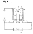
- FIG. 4 is a schematic diagram showing an electrostatic atomization device using a Peltier element cooling control circuit 10 according to one embodiment of the present invention.
- a Peltier element 1 includes a P type semiconductor 1a, an N type semiconductor 1b, an electrical connector 1c, and heat dissipation conductors 1d.
- the electrical connector 1c connects heat absorption surfaces of the P type semiconductor 1a and N type semiconductor 1b.
- the heat dissipation conductors 1d are formed from a conductive material and connected to heat dissipation surfaces of the P type semiconductor 1a and N type semiconductor 1b.
- a lead wire 1e is connected to each heat dissipation conductor 1d.
- a discharge electrode 5 is formed on the electrical connector 1c at the side facing away from the heat absorption surfaces.
- the two heat dissipation conductors 1d each have a basal portion.
- An opposing electrode 7 opposed to the discharge electrode 5 is supported in the opening at the distal end of the housing 6.
- the opposing electrode 7 is annular and connected to ground.
- a discharge hole 15 extends through the central part of the opposing electrode 7.
- the two heat dissipation conductors 1d of the Peltier element 1 are electrically connected to a current path, which includes the lead wires 1e.
- the current path is connected to the cooling control circuit 10 and a high voltage application unit 11, which applies high voltage to the discharge electrode 5.
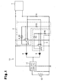
- the cooling control circuit 10 includes a DC power supply 12 ( Fig. 1 ).
- the cooling control circuit 10 controls the cooling of the Peltier element 1 and cools the electrical connector 1c and the discharge electrode 5, which are located on the heat absorption side. When cooling the discharge electrode 5 in this manner, the moisture in the air is cooled. This generates condensed water on the discharge electrode 5. The generation of condensed water supplies the discharge electrode 5 with water. Heat is dissipated from the heat dissipation conductors 1d.
- a current control circuit IC of the cooling control circuit 10 performs cooling control on the Peltier element 1 based on voltage, which is proportional to the current flowing through the Peltier element 1.
- the cooling control includes constant current control performed when the ambient temperature is greater than or equal to a predetermined temperature.
- the cooling control also includes current control performed to decrease the current as the ambient temperature decreases when the ambient temperature is less than the predetermined temperature.
- Fig. 1 is a schematic circuit diagram of the cooling control circuit 10 according to one embodiment of the present invention.
- the cooling control circuit 10 performs control in accordance with the ambient temperature as shown in Fig. 2 .
- the cooling control circuit 10 includes a current detection resistor R1 and the current control circuit IC.
- the current detection resistor R1 detects the current flowing to the Peltier element 1.
- the current control circuit performs current control on the Peltier element 1 based on the voltage that is proportional to the current flowing to the Peltier element 1.
- the cooling control circuit 10 further includes first and second amplification circuits 2 and 3 connected between the current detection resistor R1 and the current control circuit IC.
- the first amplification circuit 2 includes an operational amplifier OP1 and two resistors R2 and R3, which are connected in series between a first terminal of the resistor R1 and an output terminal of the operational amplifier OP1.
- the two resistors R2 and R3 determine the amplification rate of the operational amplifier OP1.
- the resistor R2 is a thermistor 4.
- the thermistor 4 has a first end (node between the resistors R2 and R3), which is connected to an inverting input terminal of the operational amplifier OP1, and a second end, which is connected to an output terminal of the operational amplifier OP1.
- the operational amplifier OP1 has a non-inverting input terminal connected to a second terminal of the resistor R1 and the corresponding heat dissipation conductor 1d of the Peltier element 1.
- the second amplification circuit 3 includes an operational amplifier OP2 and two resistors R4 and R5, which are connected in series between the first terminal of the resistor R1 and an output terminal of the operational amplifier OP2.
- the two resistors R4 and R5 determine the amplification rate of the operational amplifier OP2.
- the resistor R4 has a first end (node between the resistors R4 and R5), which is connected to an inverting input terminal of the operational amplifier OP2, and a second end, which is connected to an output terminal of the operational amplifier OP2.
- the operational amplifier OP2 has a non-inverting input terminal connected to the second terminal of the resistor R1 and the corresponding heat dissipation conductor 1d of the Peltier element 1.
- An output terminal of the operational amplifier OP1 in the first amplification circuit 2 is connected to an anode of a first diode 8.
- An output terminal of the operational amplifier OP2 in the second amplification circuit 3 is connected to an anode of a second diode 9.
- the first and second diodes 8 and 9 each have a cathode connected to the current control circuit IC.
- the first and second amplification circuits 2 and 3 are configured so as to input the larger one of the output voltages of the first and second amplification circuits 2 and 3 to the current control circuit IC.
- the thermistor 4 which forms the resistor R2 in the first amplification circuit 2, is used to detect the ambient temperature. More specifically, in the present embodiment, the thermistor 4 detects the ambient temperature in the area the electrostatic atomization device is arranged. It is preferable that the thermistor 4 be arranged at a location at which the influence of a temperature rise is minimal.
- the thermistor 4 has the temperature characteristics that are shown by the relationship of the temperature and resistance in the graph of Fig. 3 .
- the current detection resistor R1 detects the current flowing to the Peltier element 1.
- the first amplification circuit 2 amplifies voltage that is proportional to the detected current in accordance with the amplification rate determined by the resistance corresponding to the temperature characteristics of the thermistor 4 and the resistance of the resistor R3.
- the amplified voltage is supplied via the first diode 8 to the current control circuit IC.
- the second amplification circuit 3 amplifies voltage that is proportional to the detected current in accordance with the amplification rate determined by the resistances of the resistors R4 and R5.
- the amplified voltage is supplied via the second diode 9 to the current control circuit IC.
- the amplification rates of the first and second amplification circuits 2 and 3 are set so that the output voltage of the second amplification circuit 3 becomes greater than the output voltage of the first amplification circuit 2 when the ambient temperature is greater than or equal to a predetermined temperature and the output voltage of the first amplification circuit 2 is greater than the output voltage of the second amplification circuit 3 when the ambient temperature is less than the predetermined temperature. Accordingly, the output voltages of the first and second amplification circuits 2 and 3 are automatically selected in accordance with the ambient temperature.
- the cooling control of the Peltier element 1 is performed with a simple structure and without using a microcomputer.
- the current control circuit IC when the ambient temperature is greater than or equal to the predetermined temperature, the current control circuit IC receives the output voltage of the second amplification circuit 3 and controls the current supplied to the Peltier element 1 so as to be constant. When the ambient temperature is less than the predetermined temperature, the current control circuit IC receives the output voltage of the first amplification circuit 2 and controls the current supplied to the Peltier element 1 in accordance with the temperature characteristics of the thermistor 4 as shown in Fig. 3 .
- the Peltier element 1 undergoes constant current control with the output voltage of the second amplification circuit 3. Accordingly, when the ambient temperature is greater than or equal to the predetermined temperature, the current does not increase as the temperature increases. This prolongs the life of the Peltier element 1 under high temperatures.
- the Peltier element 1 undergoes current control with the output voltage of the first amplification circuit 2 based on the temperature characteristics of the thermistor 4 as shown in Fig. 3 . Accordingly, when the ambient temperature is low and less than the predetermined temperature, the Peltier element 1 is controlled so that the current decreases as the ambient temperature decreases. The Peltier element 1 does not become too low such that the condensed water freezes, and the condensed water is generated in a satisfactory manner. This stabilizes electrostatic atomization.
- the gradient of the temperature characteristics of the thermistor 4 for performing current control which decreases the current as the ambient temperature decreases when the ambient temperature is less than the predetermined temperature, is achieved by selecting the B characteristic for the thermistor.
- the Peltier element 1 is not restricted to the embodiment shown in Fig. 4 .
- a plurality of Peltier elements each including a P type semiconductor 1a and an N type semiconductor 1b, may be connected in series.
- a discharge electrode discrete from the electrical connector 1c may be used instead of the discharge electrode 5 that projects from the electrical connector 1c, which is connected to the heat absorption surface of the Peltier element 1, a discharge electrode discrete from the electrical connector 1c may be used. In this case, a basal portion of the discharge electrode is connected to the electrical connector 1c.
- the present invention may be applied to an electrostatic atomization device that does not include an opposing electrode.
Landscapes
- Physics & Mathematics (AREA)
- General Physics & Mathematics (AREA)
- Engineering & Computer Science (AREA)
- Automation & Control Theory (AREA)
- Control Of Temperature (AREA)
- Electrostatic Spraying Apparatus (AREA)
- Cooling Or The Like Of Semiconductors Or Solid State Devices (AREA)
Claims (6)
- Eine Kühl-Steuerschaltung für ein Peltier-Element, wobei die Kühl-Steuerschaltung aufweist:einen Stromerfassungswiderstand, der zum Erfassen von zum Peltier-Element fließendem Strom verwendet wird und einen mit dem Peltier-Element verbundenen ersten Anschluss und einen zweiten Anschluss aufweist;einen erstenVerstärkerschaltkreis, der aufweist:einen ersten operativen Verstärker, der einen nicht-invertierenden, mit dem ersten Anschluss des Stromerfassungswiderstandes verbundenen Eingabeanschluss, einen invertierenden Eingabeanschluss und einen Ausgabeanschluss aufweist,einen ersten Widerstand, der eine Thermistor aufweist und zwischen dem invertierenden Eingabeanschluss des ersten operativen Verstärkers und dem Ausgabeanschluss des ersten Verstärkers angeschlossen ist; undeinen zweiten Widerstand, der zwischen dem zweiten Anschluss des Stromerfassungswiderstandes und dem invertierenden Eingabeanschluss des ersten operativen Verstärkers angeschlossen ist;einen zweiten Verstärkerschaltkreis, der aufweist:einen zweiten operativen Verstärker, der einen nicht-invertierenden, mit dem ersten Anschluss des Stromerfassungswiderstandes verbundenen Eingabeanschluss, einen invertierenden Eingabeanschluss und einen Ausgabeanschluss aufweist,einen dritten Widerstand, der zwischen dem invertierenden Eingabeanschluss des zweiten operativen Verstärkers und dem Ausgabeanschluss des zweiten Verstärkers angeschlossen ist; undeinen vierten Widerstand, der zwischen dem zweiten Anschluss des Stromerfassungswiderstandes und dem invertiemeden Eingabeanschluss des zweiten operativen Verstärkers angeschlossen ist; undeinen Strom-Kontrollschaltkreis, der eine Ausgabespannung des zweiten Verstärkerschaltkreises empfängt, wenn die Umgebungstemperatur größer oder gleich einer vorbestimmten Temperatur ist, und den zum Peltier-Element fließenden Strom so steuert, dass er auf Grundlage der Ausgabespannung des zweiten Verstärkerschaltkreises konstant ist, und der eine Ausgabespannung des ersten Verstärkerschaltkreises empfängt, die der Temperaturcharakteristik des Thermistors entspricht, wenn die Umgebungstemperatur kleiner ist als die vorbestimmte Temperatur, und der den zum Peltierelement fließenden Strom auf Grundlage der Ausgabespannung des ersten Verstärkerschaltkreises steuert.
- Die Kühl-Steuerschaltung gemäß Anspruch 1,
wobei der erste und der zweite Verstärkerschaltkreis so eingerichtet sind, dass die Ausgabespannung des zweiten Verstärkerschaltkreises größer ist als die Ausgabespannung des ersten Verstärkerschaltkreises, wenn die Umgebungstemperatur größer oder gleich der vorbestimmten Temperatur ist, und dass die Ausgabespannung des ersten Verstärkerschaltkreises größer ist als die Ausgabespannung des zweiten Verstärkerschaltkreises, wenn die Umgebungstemperatur kleiner als die vorbestimmte Temperatur ist. - Die Kühl-Steuerschaltung gemäß Anspruch 1,
wobei die Widerstände der ersten bis vierten Widerstände so gesetzt sind, dass die Ausgabspannung des zweiten Verstärkerschaltkreises größer ist als die Ausgabespannung des ersten Verstärkerschaltkreises, wenn die Umgebungstemperatur größer oder gleich der vorbestimmten Temperatur ist, und dass die Ausgabespannung des ersten Verstärkerschaltkreises größer als die Ausgabespannung des zweiten Verstärkerschaltkreises ist, wenn die Umgebungstemperatur kleiner als die vorbestimmte Temperstur ist. - Die Kühl-Steuerschaltung gemäß Anspruch 1,
wobei die Temperaturcharakteristiken des Thermistors so gesetzt sind, dass der zum Peltier-Element fließende Strom mit dem Sinken der Umgebungstemperatur abfällt, wenn die Umgebungstemperatur kleiner als die vorbestimmte Temperatur ist. - Die Kühl-Steuerschaltung gemäß Anspruch 1,
wobei der erste Verstärkerschaltkreis eine Spannung verstärkt, die proportional ist zum durch den Stromerfassungswiderstand erfassten Strom gemäß einer Verstärkungsrate, die durch den Widerstand entsprechend den Temperaturcharakteristiken des Thermistors und einem Widerstand des zweiten Widerstandes bestimmt ist,
und wobei der zweite Verstärkerschaltkreis eine Spannung verstärkt, die proportional ist zum durch den Stromerfassungswiderstand erfassten Strom mit einer Verstärkungsrate, die durch die Widerstände des dritten und vierten Widerstandes bestimmt wird. - Die Kühl-Steuerschaltung gemäß Anspruch 5,
wobei die Temperaturcharakteristiken des Thermistors so gesetzt sind, dass der zum Peltier-Element fließende Strom mit dem Sinken der Umgebungstemperatur abfällt, wenn die Umgebungstemperatur kleiner als die vorbestimmte Temperatur ist.
Applications Claiming Priority (2)
| Application Number | Priority Date | Filing Date | Title |
|---|---|---|---|
| JP2009221517A JP5308294B2 (ja) | 2009-09-25 | 2009-09-25 | ペルチェ素子の冷却制御回路 |
| PCT/JP2010/066742 WO2011037243A2 (en) | 2009-09-25 | 2010-09-21 | Cooling control circuit for peltier element |
Publications (2)
| Publication Number | Publication Date |
|---|---|
| EP2480945A2 EP2480945A2 (de) | 2012-08-01 |
| EP2480945B1 true EP2480945B1 (de) | 2014-04-30 |
Family
ID=43796320
Family Applications (1)
| Application Number | Title | Priority Date | Filing Date |
|---|---|---|---|
| EP10763883.5A Active EP2480945B1 (de) | 2009-09-25 | 2010-09-21 | Kühlsteuerkreis für peltier-element |
Country Status (6)
| Country | Link |
|---|---|
| US (1) | US8689569B2 (de) |
| EP (1) | EP2480945B1 (de) |
| JP (1) | JP5308294B2 (de) |
| CN (1) | CN102656533B (de) |
| TW (1) | TW201133170A (de) |
| WO (1) | WO2011037243A2 (de) |
Families Citing this family (8)
| Publication number | Priority date | Publication date | Assignee | Title |
|---|---|---|---|---|
| JP5206814B2 (ja) * | 2011-02-02 | 2013-06-12 | カシオ計算機株式会社 | 冷却装置、冷却制御方法及びプログラム |
| US9587872B2 (en) | 2012-12-03 | 2017-03-07 | Whirlpool Corporation | Refrigerator with thermoelectric device control process for an icemaker |
| US9593870B2 (en) | 2012-12-03 | 2017-03-14 | Whirlpool Corporation | Refrigerator with thermoelectric device for ice making |
| JP2014231933A (ja) | 2013-05-28 | 2014-12-11 | パナソニック株式会社 | 冷却制御回路及びそれを備える静電霧化装置 |
| JP5963092B2 (ja) * | 2013-11-07 | 2016-08-03 | Smc株式会社 | 温調装置 |
| FR3076395B1 (fr) * | 2017-12-28 | 2020-01-17 | Thales | Dispositif de controle thermique d'un composant, systeme electronique et plate-forme associes |
| US11262776B2 (en) * | 2019-06-27 | 2022-03-01 | International Business Machines Corporation | Modifying regulator output voltage with a peltier device |
| CN114152010B (zh) * | 2020-09-07 | 2023-08-22 | 圣邦微电子(北京)股份有限公司 | 热电致冷致热器的控制器及控制方法 |
Family Cites Families (17)
| Publication number | Priority date | Publication date | Assignee | Title |
|---|---|---|---|---|
| US3303537A (en) * | 1964-04-07 | 1967-02-14 | Systems Matrix Inc | Safety ejection control for casting machines |
| US3195345A (en) * | 1964-05-11 | 1965-07-20 | Cambridge Systems Inc | Thermoelectric dewpoint determining system |
| US3435223A (en) * | 1966-04-11 | 1969-03-25 | Gen Signal Corp | Stabilization of an infrared detector cell as used in thermal wheel scanner systems |
| US3496837A (en) * | 1967-07-14 | 1970-02-24 | Union Oil Co | Method of operating a hydraulic device |
| JPH07288351A (ja) * | 1994-04-19 | 1995-10-31 | Fujitsu Ltd | ペルチェ制御回路及びその素子構造 |
| JPH10187253A (ja) * | 1996-12-27 | 1998-07-14 | Ando Electric Co Ltd | 光半導体素子の温度制御装置 |
| JP4080593B2 (ja) * | 1998-05-11 | 2008-04-23 | 浜松ホトニクス株式会社 | 光センサ |
| US6094918A (en) * | 1998-09-14 | 2000-08-01 | Nortel Networks Corporation | Thermoelectric cooler control circuit |
| MY125106A (en) * | 2000-11-01 | 2006-07-31 | Aster Gunasekera Darren | Automatic vehicle ventilation device |
| JP3851809B2 (ja) * | 2000-12-06 | 2006-11-29 | 住友電気工業株式会社 | 半導体レーザモジュール |
| US6826916B2 (en) * | 2001-04-24 | 2004-12-07 | The Furukawa Electric Co., Ltd. | Laser module, Peltier module, and Peltier module integrated heat spreader |
| JP3866059B2 (ja) * | 2001-07-09 | 2007-01-10 | 富士通株式会社 | 温度制御装置、温度制御方法及びデバイス |
| US7049558B2 (en) * | 2003-01-27 | 2006-05-23 | Arcturas Bioscience, Inc. | Apparatus and method for heating microfluidic volumes and moving fluids |
| US7082772B2 (en) * | 2003-08-20 | 2006-08-01 | Directed Electronics, Inc. | Peltier temperature control system for electronic components |
| JP4581561B2 (ja) * | 2004-06-18 | 2010-11-17 | パナソニック電工株式会社 | 静電霧化装置 |
| JP4821304B2 (ja) * | 2005-12-19 | 2011-11-24 | パナソニック電工株式会社 | 静電霧化装置 |
| CN100527037C (zh) * | 2007-07-27 | 2009-08-12 | 吉林大学 | 高稳定度恒温控制器 |
-
2009
- 2009-09-25 JP JP2009221517A patent/JP5308294B2/ja active Active
-
2010
- 2010-09-21 WO PCT/JP2010/066742 patent/WO2011037243A2/en not_active Ceased
- 2010-09-21 TW TW099131997A patent/TW201133170A/zh unknown
- 2010-09-21 CN CN201080039554.2A patent/CN102656533B/zh active Active
- 2010-09-21 EP EP10763883.5A patent/EP2480945B1/de active Active
- 2010-09-21 US US13/393,021 patent/US8689569B2/en active Active
Also Published As
| Publication number | Publication date |
|---|---|
| US8689569B2 (en) | 2014-04-08 |
| CN102656533A (zh) | 2012-09-05 |
| TW201133170A (en) | 2011-10-01 |
| WO2011037243A3 (en) | 2011-06-30 |
| EP2480945A2 (de) | 2012-08-01 |
| US20120151940A1 (en) | 2012-06-21 |
| JP5308294B2 (ja) | 2013-10-09 |
| WO2011037243A2 (en) | 2011-03-31 |
| CN102656533B (zh) | 2014-07-16 |
| JP2011070446A (ja) | 2011-04-07 |
Similar Documents
| Publication | Publication Date | Title |
|---|---|---|
| EP2480945B1 (de) | Kühlsteuerkreis für peltier-element | |
| JP5431994B2 (ja) | 電流制限回路 | |
| JP6070817B2 (ja) | 電気ケーブル、及び、電源装置 | |
| US6725669B2 (en) | Thermoelectric cooler temperature control | |
| US9829900B2 (en) | Voltage regulator | |
| CN105393068A (zh) | 冷却控制电路以及具备该冷却控制电路的静电雾化装置 | |
| JPWO2018168981A1 (ja) | 電流検出器 | |
| CN100585980C (zh) | 调节功率的控制装置和方法 | |
| JP2014062826A (ja) | バッテリ用内部抵抗測定装置 | |
| KR100685000B1 (ko) | 온도 감지장치 및 이를 포함하는 컴퓨터 | |
| US20080018402A1 (en) | Systems and arrangements for sensing current with a low loss sense element | |
| JP3114966B2 (ja) | 直流安定化電源装置 | |
| JP2015108543A (ja) | 温度検出装置 | |
| US11908621B2 (en) | Inductive-load control circuit | |
| US20140152313A1 (en) | Battery sensor | |
| CN118362931A (zh) | 监测电路及电源老化测试装置 | |
| WO2022193881A1 (zh) | 用于监测电流源的电流检测电路和集成电路 | |
| JP2018133252A (ja) | 検出装置、車両用灯具 | |
| JP3239052B2 (ja) | 半導体集積回路 | |
| US12061124B2 (en) | Circuit to compensate for temperature impedance drift of conductive component | |
| JP7552471B2 (ja) | ラッチ回路及び給電制御装置 | |
| JP2025515864A (ja) | 温度コントローラ回路、装置及び方法 | |
| JPH10126958A (ja) | 電源装置の過電流保護回路 | |
| CN112865016A (zh) | 主板保护电路、方法及终端 | |
| JPS62219680A (ja) | 半導体レ−ザ定出力駆動回路 |
Legal Events
| Date | Code | Title | Description |
|---|---|---|---|
| PUAI | Public reference made under article 153(3) epc to a published international application that has entered the european phase |
Free format text: ORIGINAL CODE: 0009012 |
|
| 17P | Request for examination filed |
Effective date: 20120228 |
|
| AK | Designated contracting states |
Kind code of ref document: A2 Designated state(s): AL AT BE BG CH CY CZ DE DK EE ES FI FR GB GR HR HU IE IS IT LI LT LU LV MC MK MT NL NO PL PT RO SE SI SK SM TR |
|
| DAX | Request for extension of the european patent (deleted) | ||
| GRAP | Despatch of communication of intention to grant a patent |
Free format text: ORIGINAL CODE: EPIDOSNIGR1 |
|
| INTG | Intention to grant announced |
Effective date: 20131203 |
|
| RIN1 | Information on inventor provided before grant (corrected) |
Inventor name: YAMASHITA, MIKIHIRO Inventor name: URATANI, YUTAKA |
|
| GRAP | Despatch of communication of intention to grant a patent |
Free format text: ORIGINAL CODE: EPIDOSNIGR1 |
|
| GRAS | Grant fee paid |
Free format text: ORIGINAL CODE: EPIDOSNIGR3 |
|
| INTG | Intention to grant announced |
Effective date: 20140224 |
|
| GRAA | (expected) grant |
Free format text: ORIGINAL CODE: 0009210 |
|
| RIN1 | Information on inventor provided before grant (corrected) |
Inventor name: URATANI, YUTAKA Inventor name: YAMASHITA, MIKIHIRO |
|
| AK | Designated contracting states |
Kind code of ref document: B1 Designated state(s): AL AT BE BG CH CY CZ DE DK EE ES FI FR GB GR HR HU IE IS IT LI LT LU LV MC MK MT NL NO PL PT RO SE SI SK SM TR |
|
| REG | Reference to a national code |
Ref country code: GB Ref legal event code: FG4D Ref country code: CH Ref legal event code: EP |
|
| REG | Reference to a national code |
Ref country code: AT Ref legal event code: REF Ref document number: 665520 Country of ref document: AT Kind code of ref document: T Effective date: 20140515 |
|
| REG | Reference to a national code |
Ref country code: IE Ref legal event code: FG4D |
|
| REG | Reference to a national code |
Ref country code: DE Ref legal event code: R096 Ref document number: 602010015649 Country of ref document: DE Effective date: 20140612 |
|
| REG | Reference to a national code |
Ref country code: AT Ref legal event code: MK05 Ref document number: 665520 Country of ref document: AT Kind code of ref document: T Effective date: 20140430 |
|
| REG | Reference to a national code |
Ref country code: LT Ref legal event code: MG4D |
|
| REG | Reference to a national code |
Ref country code: NL Ref legal event code: VDEP Effective date: 20140430 |
|
| PG25 | Lapsed in a contracting state [announced via postgrant information from national office to epo] |
Ref country code: FI Free format text: LAPSE BECAUSE OF FAILURE TO SUBMIT A TRANSLATION OF THE DESCRIPTION OR TO PAY THE FEE WITHIN THE PRESCRIBED TIME-LIMIT Effective date: 20140430 Ref country code: BG Free format text: LAPSE BECAUSE OF FAILURE TO SUBMIT A TRANSLATION OF THE DESCRIPTION OR TO PAY THE FEE WITHIN THE PRESCRIBED TIME-LIMIT Effective date: 20140730 Ref country code: GR Free format text: LAPSE BECAUSE OF FAILURE TO SUBMIT A TRANSLATION OF THE DESCRIPTION OR TO PAY THE FEE WITHIN THE PRESCRIBED TIME-LIMIT Effective date: 20140731 Ref country code: NL Free format text: LAPSE BECAUSE OF FAILURE TO SUBMIT A TRANSLATION OF THE DESCRIPTION OR TO PAY THE FEE WITHIN THE PRESCRIBED TIME-LIMIT Effective date: 20140430 Ref country code: IS Free format text: LAPSE BECAUSE OF FAILURE TO SUBMIT A TRANSLATION OF THE DESCRIPTION OR TO PAY THE FEE WITHIN THE PRESCRIBED TIME-LIMIT Effective date: 20140830 Ref country code: NO Free format text: LAPSE BECAUSE OF FAILURE TO SUBMIT A TRANSLATION OF THE DESCRIPTION OR TO PAY THE FEE WITHIN THE PRESCRIBED TIME-LIMIT Effective date: 20140730 Ref country code: CY Free format text: LAPSE BECAUSE OF FAILURE TO SUBMIT A TRANSLATION OF THE DESCRIPTION OR TO PAY THE FEE WITHIN THE PRESCRIBED TIME-LIMIT Effective date: 20140430 Ref country code: LT Free format text: LAPSE BECAUSE OF FAILURE TO SUBMIT A TRANSLATION OF THE DESCRIPTION OR TO PAY THE FEE WITHIN THE PRESCRIBED TIME-LIMIT Effective date: 20140430 |
|
| PG25 | Lapsed in a contracting state [announced via postgrant information from national office to epo] |
Ref country code: SE Free format text: LAPSE BECAUSE OF FAILURE TO SUBMIT A TRANSLATION OF THE DESCRIPTION OR TO PAY THE FEE WITHIN THE PRESCRIBED TIME-LIMIT Effective date: 20140430 Ref country code: PL Free format text: LAPSE BECAUSE OF FAILURE TO SUBMIT A TRANSLATION OF THE DESCRIPTION OR TO PAY THE FEE WITHIN THE PRESCRIBED TIME-LIMIT Effective date: 20140430 Ref country code: ES Free format text: LAPSE BECAUSE OF FAILURE TO SUBMIT A TRANSLATION OF THE DESCRIPTION OR TO PAY THE FEE WITHIN THE PRESCRIBED TIME-LIMIT Effective date: 20140430 Ref country code: LV Free format text: LAPSE BECAUSE OF FAILURE TO SUBMIT A TRANSLATION OF THE DESCRIPTION OR TO PAY THE FEE WITHIN THE PRESCRIBED TIME-LIMIT Effective date: 20140430 Ref country code: AT Free format text: LAPSE BECAUSE OF FAILURE TO SUBMIT A TRANSLATION OF THE DESCRIPTION OR TO PAY THE FEE WITHIN THE PRESCRIBED TIME-LIMIT Effective date: 20140430 Ref country code: HR Free format text: LAPSE BECAUSE OF FAILURE TO SUBMIT A TRANSLATION OF THE DESCRIPTION OR TO PAY THE FEE WITHIN THE PRESCRIBED TIME-LIMIT Effective date: 20140430 |
|
| PG25 | Lapsed in a contracting state [announced via postgrant information from national office to epo] |
Ref country code: PT Free format text: LAPSE BECAUSE OF FAILURE TO SUBMIT A TRANSLATION OF THE DESCRIPTION OR TO PAY THE FEE WITHIN THE PRESCRIBED TIME-LIMIT Effective date: 20140901 |
|
| PG25 | Lapsed in a contracting state [announced via postgrant information from national office to epo] |
Ref country code: CZ Free format text: LAPSE BECAUSE OF FAILURE TO SUBMIT A TRANSLATION OF THE DESCRIPTION OR TO PAY THE FEE WITHIN THE PRESCRIBED TIME-LIMIT Effective date: 20140430 Ref country code: BE Free format text: LAPSE BECAUSE OF FAILURE TO SUBMIT A TRANSLATION OF THE DESCRIPTION OR TO PAY THE FEE WITHIN THE PRESCRIBED TIME-LIMIT Effective date: 20140430 Ref country code: DK Free format text: LAPSE BECAUSE OF FAILURE TO SUBMIT A TRANSLATION OF THE DESCRIPTION OR TO PAY THE FEE WITHIN THE PRESCRIBED TIME-LIMIT Effective date: 20140430 Ref country code: RO Free format text: LAPSE BECAUSE OF FAILURE TO SUBMIT A TRANSLATION OF THE DESCRIPTION OR TO PAY THE FEE WITHIN THE PRESCRIBED TIME-LIMIT Effective date: 20140430 Ref country code: EE Free format text: LAPSE BECAUSE OF FAILURE TO SUBMIT A TRANSLATION OF THE DESCRIPTION OR TO PAY THE FEE WITHIN THE PRESCRIBED TIME-LIMIT Effective date: 20140430 Ref country code: SK Free format text: LAPSE BECAUSE OF FAILURE TO SUBMIT A TRANSLATION OF THE DESCRIPTION OR TO PAY THE FEE WITHIN THE PRESCRIBED TIME-LIMIT Effective date: 20140430 |
|
| REG | Reference to a national code |
Ref country code: DE Ref legal event code: R097 Ref document number: 602010015649 Country of ref document: DE |
|
| PLBE | No opposition filed within time limit |
Free format text: ORIGINAL CODE: 0009261 |
|
| STAA | Information on the status of an ep patent application or granted ep patent |
Free format text: STATUS: NO OPPOSITION FILED WITHIN TIME LIMIT |
|
| 26N | No opposition filed |
Effective date: 20150202 |
|
| PG25 | Lapsed in a contracting state [announced via postgrant information from national office to epo] |
Ref country code: MC Free format text: LAPSE BECAUSE OF FAILURE TO SUBMIT A TRANSLATION OF THE DESCRIPTION OR TO PAY THE FEE WITHIN THE PRESCRIBED TIME-LIMIT Effective date: 20140430 Ref country code: LU Free format text: LAPSE BECAUSE OF FAILURE TO SUBMIT A TRANSLATION OF THE DESCRIPTION OR TO PAY THE FEE WITHIN THE PRESCRIBED TIME-LIMIT Effective date: 20140921 |
|
| REG | Reference to a national code |
Ref country code: CH Ref legal event code: PL |
|
| REG | Reference to a national code |
Ref country code: DE Ref legal event code: R097 Ref document number: 602010015649 Country of ref document: DE Effective date: 20150202 |
|
| GBPC | Gb: european patent ceased through non-payment of renewal fee |
Effective date: 20140921 |
|
| REG | Reference to a national code |
Ref country code: IE Ref legal event code: MM4A |
|
| REG | Reference to a national code |
Ref country code: FR Ref legal event code: ST Effective date: 20150529 |
|
| PG25 | Lapsed in a contracting state [announced via postgrant information from national office to epo] |
Ref country code: LI Free format text: LAPSE BECAUSE OF NON-PAYMENT OF DUE FEES Effective date: 20140930 Ref country code: SI Free format text: LAPSE BECAUSE OF FAILURE TO SUBMIT A TRANSLATION OF THE DESCRIPTION OR TO PAY THE FEE WITHIN THE PRESCRIBED TIME-LIMIT Effective date: 20140430 Ref country code: GB Free format text: LAPSE BECAUSE OF NON-PAYMENT OF DUE FEES Effective date: 20140921 Ref country code: CH Free format text: LAPSE BECAUSE OF NON-PAYMENT OF DUE FEES Effective date: 20140930 |
|
| PG25 | Lapsed in a contracting state [announced via postgrant information from national office to epo] |
Ref country code: IE Free format text: LAPSE BECAUSE OF NON-PAYMENT OF DUE FEES Effective date: 20140921 Ref country code: IT Free format text: LAPSE BECAUSE OF NON-PAYMENT OF DUE FEES Effective date: 20140921 Ref country code: FR Free format text: LAPSE BECAUSE OF NON-PAYMENT OF DUE FEES Effective date: 20140930 |
|
| PG25 | Lapsed in a contracting state [announced via postgrant information from national office to epo] |
Ref country code: SM Free format text: LAPSE BECAUSE OF FAILURE TO SUBMIT A TRANSLATION OF THE DESCRIPTION OR TO PAY THE FEE WITHIN THE PRESCRIBED TIME-LIMIT Effective date: 20140430 |
|
| PG25 | Lapsed in a contracting state [announced via postgrant information from national office to epo] |
Ref country code: MT Free format text: LAPSE BECAUSE OF FAILURE TO SUBMIT A TRANSLATION OF THE DESCRIPTION OR TO PAY THE FEE WITHIN THE PRESCRIBED TIME-LIMIT Effective date: 20140430 |
|
| PG25 | Lapsed in a contracting state [announced via postgrant information from national office to epo] |
Ref country code: HU Free format text: LAPSE BECAUSE OF FAILURE TO SUBMIT A TRANSLATION OF THE DESCRIPTION OR TO PAY THE FEE WITHIN THE PRESCRIBED TIME-LIMIT; INVALID AB INITIO Effective date: 20100921 Ref country code: TR Free format text: LAPSE BECAUSE OF FAILURE TO SUBMIT A TRANSLATION OF THE DESCRIPTION OR TO PAY THE FEE WITHIN THE PRESCRIBED TIME-LIMIT Effective date: 20140430 |
|
| PG25 | Lapsed in a contracting state [announced via postgrant information from national office to epo] |
Ref country code: MK Free format text: LAPSE BECAUSE OF FAILURE TO SUBMIT A TRANSLATION OF THE DESCRIPTION OR TO PAY THE FEE WITHIN THE PRESCRIBED TIME-LIMIT Effective date: 20140430 |
|
| PG25 | Lapsed in a contracting state [announced via postgrant information from national office to epo] |
Ref country code: AL Free format text: LAPSE BECAUSE OF FAILURE TO SUBMIT A TRANSLATION OF THE DESCRIPTION OR TO PAY THE FEE WITHIN THE PRESCRIBED TIME-LIMIT Effective date: 20140430 |
|
| PGFP | Annual fee paid to national office [announced via postgrant information from national office to epo] |
Ref country code: DE Payment date: 20250919 Year of fee payment: 16 |