EP2479763A1 - Transparent conductive film and device comprising same - Google Patents
Transparent conductive film and device comprising same Download PDFInfo
- Publication number
- EP2479763A1 EP2479763A1 EP10817256A EP10817256A EP2479763A1 EP 2479763 A1 EP2479763 A1 EP 2479763A1 EP 10817256 A EP10817256 A EP 10817256A EP 10817256 A EP10817256 A EP 10817256A EP 2479763 A1 EP2479763 A1 EP 2479763A1
- Authority
- EP
- European Patent Office
- Prior art keywords
- transparent conductive
- conductive film
- atoms
- cerium
- hydrogen
- Prior art date
- Legal status (The legal status is an assumption and is not a legal conclusion. Google has not performed a legal analysis and makes no representation as to the accuracy of the status listed.)
- Withdrawn
Links
Images



Classifications
-
- H—ELECTRICITY
- H01—ELECTRIC ELEMENTS
- H01B—CABLES; CONDUCTORS; INSULATORS; SELECTION OF MATERIALS FOR THEIR CONDUCTIVE, INSULATING OR DIELECTRIC PROPERTIES
- H01B1/00—Conductors or conductive bodies characterised by the conductive materials; Selection of materials as conductors
- H01B1/06—Conductors or conductive bodies characterised by the conductive materials; Selection of materials as conductors mainly consisting of other non-metallic substances
- H01B1/08—Conductors or conductive bodies characterised by the conductive materials; Selection of materials as conductors mainly consisting of other non-metallic substances oxides
-
- C—CHEMISTRY; METALLURGY
- C23—COATING METALLIC MATERIAL; COATING MATERIAL WITH METALLIC MATERIAL; CHEMICAL SURFACE TREATMENT; DIFFUSION TREATMENT OF METALLIC MATERIAL; COATING BY VACUUM EVAPORATION, BY SPUTTERING, BY ION IMPLANTATION OR BY CHEMICAL VAPOUR DEPOSITION, IN GENERAL; INHIBITING CORROSION OF METALLIC MATERIAL OR INCRUSTATION IN GENERAL
- C23C—COATING METALLIC MATERIAL; COATING MATERIAL WITH METALLIC MATERIAL; SURFACE TREATMENT OF METALLIC MATERIAL BY DIFFUSION INTO THE SURFACE, BY CHEMICAL CONVERSION OR SUBSTITUTION; COATING BY VACUUM EVAPORATION, BY SPUTTERING, BY ION IMPLANTATION OR BY CHEMICAL VAPOUR DEPOSITION, IN GENERAL
- C23C14/00—Coating by vacuum evaporation, by sputtering or by ion implantation of the coating forming material
- C23C14/06—Coating by vacuum evaporation, by sputtering or by ion implantation of the coating forming material characterised by the coating material
- C23C14/08—Oxides
-
- C—CHEMISTRY; METALLURGY
- C23—COATING METALLIC MATERIAL; COATING MATERIAL WITH METALLIC MATERIAL; CHEMICAL SURFACE TREATMENT; DIFFUSION TREATMENT OF METALLIC MATERIAL; COATING BY VACUUM EVAPORATION, BY SPUTTERING, BY ION IMPLANTATION OR BY CHEMICAL VAPOUR DEPOSITION, IN GENERAL; INHIBITING CORROSION OF METALLIC MATERIAL OR INCRUSTATION IN GENERAL
- C23C—COATING METALLIC MATERIAL; COATING MATERIAL WITH METALLIC MATERIAL; SURFACE TREATMENT OF METALLIC MATERIAL BY DIFFUSION INTO THE SURFACE, BY CHEMICAL CONVERSION OR SUBSTITUTION; COATING BY VACUUM EVAPORATION, BY SPUTTERING, BY ION IMPLANTATION OR BY CHEMICAL VAPOUR DEPOSITION, IN GENERAL
- C23C14/00—Coating by vacuum evaporation, by sputtering or by ion implantation of the coating forming material
- C23C14/22—Coating by vacuum evaporation, by sputtering or by ion implantation of the coating forming material characterised by the process of coating
- C23C14/24—Vacuum evaporation
- C23C14/32—Vacuum evaporation by explosion; by evaporation and subsequent ionisation of the vapours, e.g. ion-plating
-
- H—ELECTRICITY
- H01—ELECTRIC ELEMENTS
- H01B—CABLES; CONDUCTORS; INSULATORS; SELECTION OF MATERIALS FOR THEIR CONDUCTIVE, INSULATING OR DIELECTRIC PROPERTIES
- H01B5/00—Non-insulated conductors or conductive bodies characterised by their form
- H01B5/14—Non-insulated conductors or conductive bodies characterised by their form comprising conductive layers or films on insulating-supports
-
- H—ELECTRICITY
- H05—ELECTRIC TECHNIQUES NOT OTHERWISE PROVIDED FOR
- H05B—ELECTRIC HEATING; ELECTRIC LIGHT SOURCES NOT OTHERWISE PROVIDED FOR; CIRCUIT ARRANGEMENTS FOR ELECTRIC LIGHT SOURCES, IN GENERAL
- H05B33/00—Electroluminescent light sources
- H05B33/12—Light sources with substantially two-dimensional [2D] radiating surfaces
- H05B33/26—Light sources with substantially two-dimensional [2D] radiating surfaces characterised by the composition or arrangement of the conductive material used as an electrode
- H05B33/28—Light sources with substantially two-dimensional [2D] radiating surfaces characterised by the composition or arrangement of the conductive material used as an electrode of translucent electrodes
-
- H—ELECTRICITY
- H10—SEMICONDUCTOR DEVICES; ELECTRIC SOLID-STATE DEVICES NOT OTHERWISE PROVIDED FOR
- H10F—INORGANIC SEMICONDUCTOR DEVICES SENSITIVE TO INFRARED RADIATION, LIGHT, ELECTROMAGNETIC RADIATION OF SHORTER WAVELENGTH OR CORPUSCULAR RADIATION
- H10F10/00—Individual photovoltaic cells, e.g. solar cells
-
- H—ELECTRICITY
- H10—SEMICONDUCTOR DEVICES; ELECTRIC SOLID-STATE DEVICES NOT OTHERWISE PROVIDED FOR
- H10F—INORGANIC SEMICONDUCTOR DEVICES SENSITIVE TO INFRARED RADIATION, LIGHT, ELECTROMAGNETIC RADIATION OF SHORTER WAVELENGTH OR CORPUSCULAR RADIATION
- H10F77/00—Constructional details of devices covered by this subclass
- H10F77/20—Electrodes
- H10F77/244—Electrodes made of transparent conductive layers, e.g. transparent conductive oxide [TCO] layers
-
- H—ELECTRICITY
- H10—SEMICONDUCTOR DEVICES; ELECTRIC SOLID-STATE DEVICES NOT OTHERWISE PROVIDED FOR
- H10K—ORGANIC ELECTRIC SOLID-STATE DEVICES
- H10K2102/00—Constructional details relating to the organic devices covered by this subclass
- H10K2102/10—Transparent electrodes, e.g. using graphene
- H10K2102/101—Transparent electrodes, e.g. using graphene comprising transparent conductive oxides [TCO]
- H10K2102/103—Transparent electrodes, e.g. using graphene comprising transparent conductive oxides [TCO] comprising indium oxides, e.g. ITO
-
- H—ELECTRICITY
- H10—SEMICONDUCTOR DEVICES; ELECTRIC SOLID-STATE DEVICES NOT OTHERWISE PROVIDED FOR
- H10K—ORGANIC ELECTRIC SOLID-STATE DEVICES
- H10K30/00—Organic devices sensitive to infrared radiation, light, electromagnetic radiation of shorter wavelength or corpuscular radiation
- H10K30/80—Constructional details
- H10K30/81—Electrodes
- H10K30/82—Transparent electrodes, e.g. indium tin oxide [ITO] electrodes
-
- Y—GENERAL TAGGING OF NEW TECHNOLOGICAL DEVELOPMENTS; GENERAL TAGGING OF CROSS-SECTIONAL TECHNOLOGIES SPANNING OVER SEVERAL SECTIONS OF THE IPC; TECHNICAL SUBJECTS COVERED BY FORMER USPC CROSS-REFERENCE ART COLLECTIONS [XRACs] AND DIGESTS
- Y02—TECHNOLOGIES OR APPLICATIONS FOR MITIGATION OR ADAPTATION AGAINST CLIMATE CHANGE
- Y02E—REDUCTION OF GREENHOUSE GAS [GHG] EMISSIONS, RELATED TO ENERGY GENERATION, TRANSMISSION OR DISTRIBUTION
- Y02E10/00—Energy generation through renewable energy sources
- Y02E10/50—Photovoltaic [PV] energy
Definitions
- the present invention relates to a transparent conductive film and a device with the same.
- Transparent conductive films have been conventionally used in various devices such as display devices like liquid display devices, organic electroluminescence devices, solar cell devices like thin film solar cells, dye-sensitized solar cells, and electronic components.
- a transparent conductive film made from indium oxide containing tin (ITO) and a transparent conductive film made from zinc oxide (ZnO) and the like are known.
- a transparent conductive film made of indium oxide containing cerium added by a spattering method is disclosed as a transparent conductive film made from indium oxide, for example.
- Patent publication 1 Japanese Patent Publication Laid-open No. Hei8-260134
- the present invention considers the above-identified problem and provides a transparent conductive film that is capable of absorbing less light of the long-wavelength side, has good carrier mobility and a lower electric resistance.
- An aspect of the present invention is a transparent conductive film that includes indium oxide containing hydrogen and cerium and has substantially polycrystalline structure, wherein the specific resistance is not greater than 3.4 x 10 -4
- the transparent conductive film is capable of absorbing less light of the long-wavelength side, having good carrier mobility and lowering the electric resistance because the transparent conductive film includes indium oxide containing hydrogen and cerium and comprises a substantially polycrystalline structure, wherein the specific resistance is not greater than 3.4 x 10 -4
- the present invention when the present invention is applied in devices such as display devices like liquid display devices, organic electroluminescence devices, solar cell devices like crystalline solar cells, thin film solar cells, dye-sensitized solar cells, and electronic components, the performance of these devices can be improved.
- the invention provides a transparent conductive film capable of absorbing less light of the long-wavelength side, having good carrier mobility and lowering the electric resistance, and a device with the same.
- a transparent conductive film according to the present invention is explained below by referring to the figures.
- substrate body 1 is a substrate body formed by a glass substrate, polycrystalline silicon substrate, monocrystalline silicon substrate, and a substantially intrinsic i-type amorphous silicon layer and a p-type amorphous silicon layer, in this order. Namely, substrate body 1 has the p-type amorphous layer on the top surface and is formed by the monocrystalline silicon substrate and the like. 2 is a transparent conductive film formed on substrate body 1.
- Transparent conductive film 2 is a film that includes indium oxide as an essential ingredient and also contains cerium (Ce) and hydrogen (H). Namely, transparent conductive film 2 includes hydrogen (H), cerium (Ce), indium (In), and oxygen (O), and contains indium oxide (In 2 O 3 ) doped with hydrogen (H)and cerium (Ce)as impurities.
- Transparent conductive film 2 is formed substantially by polycrystalline structures and contains numerous pillar-like structures bristled up to cover the substrate body. Further, transparent conductive film 2 contains a very little amount of amorphous portions.
- a hydrogen (H) content in transparent conductive film 2 is preferably 1.0 x 10 21 atoms/cm 3 and more preferably is in the order of 10 21 atoms/cm 3 .
- the hydrogen content here refers to an amount of hydrogen contained in the middle of transparent conductive film 2 in its thickness direction and is substantially the same as the average content in the film other than in the vicinities of both surfaces of transparent conductive film 2.
- the hydrogen content concentration is preferably greater in the substrate body 1 side than in the film surface side, and more preferably, the concentration increases gradually toward the substrate body 1 side.
- the specific resistance of transparent conductive film 2 is not greater than 3.4 x 10 -4 resistance of transparent conductive film 2, the better. However, the specific resistance may be between not greater than 3.4 x 10 -4 less than 1.0 x 10 -4
- a cerium (Ce) content in transparent conductive film 2 is preferably between 1.0 x 10 20 atoms/cm 3 or more and 1.4 x 10 21 atoms/cm 3 or less, and more preferably is between 2.4 x 10 20 atoms/cm 3 or more and 1.2 x 10 21 atoms/cm 3 or less, and further more preferably is between 4.8 x 10 20 atoms/cm 3 or more and 1.1 x 10 21 atoms/cm 3 or less, and still further more preferably is between 7.5 x 10 20 atoms/cm 3 or more, and 1.0 x 10 21 atoms/cm 3 or less, and yet further more preferably is between 7.5 x 10 20 atoms/cm 3 or more, and 8.5 x 10 20 atoms/cm 3 or less.
- substrate body 1 is prepared by removing impurities on the surface by cleaning.
- substrate body 1 is a body including a substantially intrinsic i-type amorphous silicon layer and a p-type amorphous silicon layer formed on an n-type monocrystalline silicon substrate in this order
- substrate body 1 is formed as follows: upon removing impurities by cleaning the n-type monocrystalline silicon substrate, a substantially intrinsic i-type amorphous silicon layer and a p-type amorphous silicon layer are formed in this order on n-type monocrystalline silicon substrate by using the RF plasma CVD method.
- the conditions of the RF plasma CVD method may be at a frequency of about 13.56 MHz, a formation temperature of approximately 100°C - 300°C, a reaction pressure of about 5Pa - 100Pa, and an RF power of about 1 mW/cm 2 - 500 mW/cm 2 . Subsequently, substrate body 1 is cleaned again.
- the transparent conductive film including indium oxide containing hydrogen (H) and cerium (Ce) as impurities is formed on substrate body 1 by using the ion plating method in an atmosphere of Ar/O 2 gas mixture and steam at a room temperature.
- a sintered body of In 2 O 3 powder that contains a predetermined amount of cerium oxide (CeO 2 ) powder as a dopant is used for ingredients.
- the amount of cerium (Ce) contained in the transparent conductive film can be changed by using the sintered body with varied contents of cerium oxide (CeO 2 ).
- the crystallization of the above-mentioned transparent conductive film is preferably proceeded by annealing at approximately 200°C for about 1 hour, thereby transparent conductive film 2 is prepared.
- a separate annealing process may not be required in case the annealing treatment is combined with other manufacturing processes.
- transparent conductive film 2 is found to include pillar-like structures that contain substantially polycrystalline structures, and a very little amount of amorphous portions.
- Fig. 2 is a table showing the amount of cerium oxide (CeO 2 ) in the sintered body used for making respective transparent conductive films, types of substrates used, contents of cerium (Ce) and contents of hydrogen in respective transparent conductive films, the specific resistance of respective transparent conductive films, carrier mobility, and carrier density in examples 1-7 according to the embodiment, and in comparative examples 1-10.
- the amount of Ce is measured by the Rutherford backscattering spectrometry (RBS) method.
- the amount of hydrogen is measured by the Hydrogen forward scattering (HFS) method.
- (111)Si substrate refers to a substrate body including an i-type amorphous silicon layer that is substantially intrinsic and has a layer thickness of approximately 5nm and a p-type amorphous silicon layer that is substantially intrinsic and has a layer thickness of approximately 5nm formed on an n-type monocrystalline silicon substrate in this order.
- Comparative examples 1-10 are manufactured using the same manufacturing method as in the embodiment except for sintered bodies and the amount of steam. Note that transparent conductive films in comparative examples 1-7 include indium oxide as an essential ingredient and also contains hydrogen (H) and cerium (Ce), and transparent conductive films in comparative examples 8-10 include indium oxide as an essential ingredient and also contains hydrogen (H) and tin (Sn).
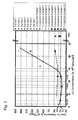
- Fig. 3 is a diagram showing the relationship between the specific resistance of the transparent conductive films and the amount of cerium (Ce) in the transparent conducive films in examples 1-7 according to the embodiment, and the transparent conducive films in comparative examples 1-10.
- the solid line indicates that the amount of hydrogen (H) in the transparent conductive film is 2.0 x 10 21 atoms/cm 3
- the broken line indicates that the amount of hydrogen (H) in the transparent conductive film is 9.0 x 10 20 atoms/cm 3 .
- the specific resistance is measured according to the Van der Pauw method using a Hall effect measuring device.
- Figs. 2 and 3 indicate that where the content of cerium (Ce) in the transparent conductive film is between 1.0 x 10 20 atoms/cm 3 or more and 1.4 x 10 21 atoms/cm 3 or less, the specific resistance is smaller (i.e., is not greater than 3.4 x 10 -4 when the amount of hydrogen (H) in the transparent conductive film is in the order of 10 21 atoms/cm 3 such as 2.0 x 10 21 atoms/cm 3 compared with that of in the order of 10 20 atoms/cm 3 such as 9.0 x 10 20 atoms/cm 3 .
- cerium (Ce) content in the transparent conductive film is preferably between 2.4 x 10 20 atoms/cm 3 or more and 1.2 x 10 21 atoms/cm 3 or less and the specific resistance is not greater than 2.5 x 10 -4 and more preferably is between 4.8 x 10 20 atoms/cm 3 or more and 1.1 x 10 21 atoms/cm 3 or less and the specific resistance is not greater than 2.2 x 10 -4 and further more preferably is between 7.5 x 10 20 atoms/cm 3 or more and 1.0 x 10 21 atoms/cm 3 or less, and still further more preferably is between 7.5 x 10 20 atoms/cm 3 or more and 8.5 x 10 20 atoms/cm 3 or less.
- Fig. 4 is a diagram showing the relationship between the carrier mobility in the transparent conductive film and the amount of cerium (Ce) in transparent conductive film 2 in examples 1-7 according to the embodiment, and the transparent conductive films in comparative examples 1-10.
- the solid line indicates that the amount of hydrogen (H) in the transparent conductive film is 2.0 x 10 21 atoms/cm 3
- the broken line indicate that the amount of hydrogen (H) in the transparent conductive film is 9.0 x 10 20 atoms/cm 3 .
- the carrier mobility is measured by using a Hall effect measuring device.
- a device performs better as an electrode when the carrier mobility value is greater because the specific resistance decreases. Therefore, it is preferable that the carrier mobility value is great.
- Figs. 2 and 4 indicate that when the cerium (Ce) content in the transparent conductive film is between 1.0 x 10 20 atoms/cm 3 or more and 1.4 x 10 21 atoms/cm 3 or less, the carrier mobility is greater (i.e., greater than 70 cm 2 /Vs) in case the amount of hydrogen (H) in the transparent conductive film is in the order of 10 21 atoms/cm 3 such as 2.0 x 10 21 atoms/cm 3 , than in case the amount of hydrogen (H) in the transparent conductive film is in the order of 10 20 atoms/cm 3 such as 9.0 x 10 20 atoms/cm 3 .
- the carrier mobility becomes greater than approximately 90 cm 2 /Vs which is preferable.
- the cerium (Ce) content in the transparent conductive film be between 2.4 x 10 20 atoms/cm 3 or more and 1.1 x 10 21 atoms/cm 3 or less, and further more preferable that it be between 4.8 x 10 20 atoms/cm 3 or more and 1.0 x 10 21 atoms/cm 3 or less, and yet further more preferable that the cerium content be between 7.5 x 10 20 atoms/cm 3 or more, and 8.5 x 10 20 atoms/cm 3 or less.
- the content of cerium (Ce) in the transparent conductive film is preferably between 1.0 x 10 20 atoms/cm 3 or more and 1.4 x 10 21 atoms/cm 3 or less, and more preferably is between 2.4 x 10 20 atoms/cm 3 or more and 1.1 x 10 21 atoms/cm 3 or less, and further more preferably between 4.8 x 10 20 atoms/cm 3 or more and 1.0 x 10 21 atoms/cm 3 or less, and still further more preferably, between 7.5 x 10 20 atoms/cm 3 or more, and 8.5 x 10 20 atoms/cm 3 or less.
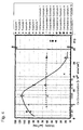
- Fig. 5 is a diagram showing the relationship between the carrier density and the amount of cerium (Ce) in transparent conductive film 2 in examples 1-7, and in transparent conductive films in comparative examples 1-10.
- the solid line indicates that the amount of hydrogen (H) in the transparent conductive film is 2.0 x 10 21 atoms/cm 3
- the broken line indicates that the amount of hydrogen (H) in the transparent conductive film is 9.0 x 10 20 atoms/cm 3 .
- the carrier mobility is measured using a Hall effect measuring device.
- the carrier density when a value of the carrier density is higher, the light with a longer wavelength is absorbed. Also, carriers themselves cause scattering. As a result, the carrier mobility is decreased. Therefore, when the specific resistance has the same value, it is preferable that the carrier density be lower. However, when the carrier density is too low, the grain boundary scattering within the film increases which results in the decrease of the carrier mobility. Therefore, it is preferable that the carrier density be within a predetermined range.
- Figs. 2 and 5 indicate that when the cerium (Ce) content in the transparent conductive film is between 1.0 x 10 20 atoms/cm 3 or more and 2.0 x 10 21 atoms/cm 3 or less, the carrier density is between 2.0 x 10 20 cm -3 or more and 3.5 x 10 20 cm -3 or less, and is in an excellent range. However, even within this content range, it is further preferable that the cerium (Ce) content be in the higher concentration or in the lower concentration of the range.
- Figs. 2-4 indicate that the transparent conductive films in comparative examples 8-10 including indium oxide as an essential ingredient and also containing hydrogen (H) and tin (Sn) exhibit the low specific resistance; however, the carrier mobility is not greater than 60 cm 2 /Vs. This result shows that transparent conductive films including indium oxide as an essential ingredient and also contains hydrogen (H) in the order of 10 21 atoms/cm 3 and cerium (Ce) is preferable.
- the transparent conductive film according to the present invention can be properly used in display devices such as liquid display devices, organic electroluminescence devices, solar cell devices such as crystalline solar cells, thin film solar cells, dye-sensitized solar cells, and electronic components.
- display devices such as liquid display devices, organic electroluminescence devices, solar cell devices such as crystalline solar cells, thin film solar cells, dye-sensitized solar cells, and electronic components.
- the transparent conductive film including a transparent conductive film having a texture structure, a first type amorphous silicon layer, a substantially intrinsic i-type amorphous silicon layer, and another amorphous silicon layer having an opposite type to the first type, and a transparent conductive film formed on a glass substrate, in this order, may be used in a thin film solar cell.
- the invention can be used in the fields of display devices such as liquid display devices, organic electroluminescence devices, solar cell devices such as crystalline solar cells, thin film solar cells, dye-sensitized solar cells, and electronic components, because the invention provides a transparent conductive film capable of absorbing less light of the long-wavelength side, having good carrier mobility and lowering the electric resistance, and a device with the same.
Landscapes
- Chemical & Material Sciences (AREA)
- Chemical Kinetics & Catalysis (AREA)
- Engineering & Computer Science (AREA)
- Materials Engineering (AREA)
- Mechanical Engineering (AREA)
- Metallurgy (AREA)
- Organic Chemistry (AREA)
- Non-Insulated Conductors (AREA)
- Electroluminescent Light Sources (AREA)
- Physical Vapour Deposition (AREA)
- Photovoltaic Devices (AREA)
Abstract
Description
- The present invention relates to a transparent conductive film and a device with the same.
- Transparent conductive films have been conventionally used in various devices such as display devices like liquid display devices, organic electroluminescence devices, solar cell devices like thin film solar cells, dye-sensitized solar cells, and electronic components.
- It is preferable that the resistance of such a transparent conductive film is small. Conventionally, a transparent conductive film made from indium oxide containing tin (ITO) and a transparent conductive film made from zinc oxide (ZnO) and the like are known. Other than the transparent conductive film containing tin (ITO), a transparent conductive film made of indium oxide containing cerium added by a spattering method is disclosed as a transparent conductive film made from indium oxide, for example. (For instance, see patent publication 1)
- Patent publication 1: Japanese Patent Publication Laid-open No.
Hei8-260134 - However, there has been a problem in making a transparent conductive film made of indium oxide containing cerium due to the difficulty in making the film absorb less light of the long-wavelength side, while having good carrier mobility and a lower electric resistance.
- The present invention considers the above-identified problem and provides a transparent conductive film that is capable of absorbing less light of the long-wavelength side, has good carrier mobility and a lower electric resistance.
- An aspect of the present invention is a transparent conductive film that includes indium oxide containing hydrogen and cerium and has substantially polycrystalline structure, wherein the specific resistance is not greater than 3.4 x 10⁻⁴
- According to the present invention, the transparent conductive film is capable of absorbing less light of the long-wavelength side, having good carrier mobility and lowering the electric resistance because the transparent conductive film includes indium oxide containing hydrogen and cerium and comprises a substantially polycrystalline structure, wherein the specific resistance is not greater than 3.4 x 10⁻⁴
- Accordingly, when the present invention is applied in devices such as display devices like liquid display devices, organic electroluminescence devices, solar cell devices like crystalline solar cells, thin film solar cells, dye-sensitized solar cells, and electronic components, the performance of these devices can be improved.
- The invention provides a transparent conductive film capable of absorbing less light of the long-wavelength side, having good carrier mobility and lowering the electric resistance, and a device with the same.
-
- [
Fig. 1] Fig. 1 is a sectional view of a transparent conductive film according to an embodiment of the present invention. - [
Fig. 2] Fig. 2 is a table showing sintered bodies used for making respective transparent conductive films, types of substrates used, contents of cerium (Ce) and contents of hydrogen in respective transparent conductive films, the specific resistance of respective transparent conductive films, carrier mobility, and carrier density in examples 1-7 according to the embodiment, and in comparative examples 1-10. - [
Fig. 3] Fig. 3 is a diagram showing the relationship between the cerium (Ce) concentration and the specific resistance in examples according to the embodiment, and in comparative examples. - [
Fig. 4] Fig. 4 is a diagram showing the relationship between the cerium (Ce) concentration and the carrier mobility in examples according to the embodiment, and in comparative examples. - [
Fig. 5] Fig. 5 is a diagram showing the relationship between the cerium (Ce) concentration and the carrier density in examples according to the embodiment, and in comparative examples. - A transparent conductive film according to the present invention is explained below by referring to the figures.
- 1 is a substrate body formed by a glass substrate, polycrystalline silicon substrate, monocrystalline silicon substrate, and a substantially intrinsic i-type amorphous silicon layer and a p-type amorphous silicon layer, in this order. Namely,
substrate body 1 has the p-type amorphous layer on the top surface and is formed by the monocrystalline silicon substrate and the like. 2 is a transparent conductive film formed onsubstrate body 1. - Transparent
conductive film 2 is a film that includes indium oxide as an essential ingredient and also contains cerium (Ce) and hydrogen (H). Namely, transparentconductive film 2 includes hydrogen (H), cerium (Ce), indium (In), and oxygen (O), and contains indium oxide (In2O3) doped with hydrogen (H)and cerium (Ce)as impurities. - Transparent
conductive film 2 is formed substantially by polycrystalline structures and contains numerous pillar-like structures bristled up to cover the substrate body. Further, transparentconductive film 2 contains a very little amount of amorphous portions. - A hydrogen (H) content in transparent
conductive film 2 is preferably 1.0 x 10²¹ atoms/cm3 and more preferably is in the order of 1021 atoms/cm3. The hydrogen content here refers to an amount of hydrogen contained in the middle of transparentconductive film 2 in its thickness direction and is substantially the same as the average content in the film other than in the vicinities of both surfaces of transparentconductive film 2. The hydrogen content concentration is preferably greater in thesubstrate body 1 side than in the film surface side, and more preferably, the concentration increases gradually toward thesubstrate body 1 side. - The specific resistance of transparent
conductive film 2 is not greater than 3.4 x 10⁻⁴ resistance of transparentconductive film 2, the better. However, the specific resistance may be between not greater than 3.4 x 10⁻⁴ less than 1.0 x 10⁻⁴ - A cerium (Ce) content in transparent
conductive film 2 is preferably between 1.0 x 10²⁰ atoms/cm3 or more and 1.4 x 10²¹ atoms/cm3 or less, and more preferably is between 2.4 x 10²⁰ atoms/cm3 or more and 1.2 x 10²¹ atoms/cm3 or less, and further more preferably is between 4.8 x 10²⁰ atoms/cm3 or more and 1.1 x 10²¹ atoms/cm3 or less, and still further more preferably is between 7.5 x 10²⁰ atoms/cm3 or more, and 1.0 x 10²¹ atoms/cm3 or less, and yet further more preferably is between 7.5 x 10²⁰ atoms/cm3 or more, and 8.5 x 10²⁰ atoms/cm3 or less. - Hereinafter, a method of manufacturing a transparent conductive film according to the embodiment is explained.
- First,
substrate body 1 is prepared by removing impurities on the surface by cleaning. - Note that in the case where
substrate body 1 is a body including a substantially intrinsic i-type amorphous silicon layer and a p-type amorphous silicon layer formed on an n-type monocrystalline silicon substrate in this order,substrate body 1 is formed as follows: upon removing impurities by cleaning the n-type monocrystalline silicon substrate, a substantially intrinsic i-type amorphous silicon layer and a p-type amorphous silicon layer are formed in this order on n-type monocrystalline silicon substrate by using the RF plasma CVD method. The conditions of the RF plasma CVD method may be at a frequency of about 13.56 MHz, a formation temperature of approximately 100°C - 300°C, a reaction pressure of about 5Pa - 100Pa, and an RF power of about 1 mW/cm2 - 500 mW/cm2. Subsequently,substrate body 1 is cleaned again. - Next, the transparent conductive film including indium oxide containing hydrogen (H) and cerium (Ce) as impurities, is formed on
substrate body 1 by using the ion plating method in an atmosphere of Ar/O2 gas mixture and steam at a room temperature. A sintered body of In2O3 powder that contains a predetermined amount of cerium oxide (CeO2) powder as a dopant is used for ingredients. In this case, the amount of cerium (Ce) contained in the transparent conductive film can be changed by using the sintered body with varied contents of cerium oxide (CeO2). - Next, the crystallization of the above-mentioned transparent conductive film is preferably proceeded by annealing at approximately 200°C for about 1 hour, thereby transparent
conductive film 2 is prepared. In manufacturing various devices, a separate annealing process may not be required in case the annealing treatment is combined with other manufacturing processes. - From the measurement results of electron backscatter diffraction (EBSD), transmission electron microscopy (TEM), and x-ray diffraction (XRD), transparent
conductive film 2 according to the embodiment is found to include pillar-like structures that contain substantially polycrystalline structures, and a very little amount of amorphous portions. -
Fig. 2 is a table showing the amount of cerium oxide (CeO2) in the sintered body used for making respective transparent conductive films, types of substrates used, contents of cerium (Ce) and contents of hydrogen in respective transparent conductive films, the specific resistance of respective transparent conductive films, carrier mobility, and carrier density in examples 1-7 according to the embodiment, and in comparative examples 1-10. Note that the amount of Ce is measured by the Rutherford backscattering spectrometry (RBS) method. The amount of hydrogen is measured by the Hydrogen forward scattering (HFS) method. - The indication of "large" in the column for "hydrogen content" refers to the content of hydrogen in a transparent conductive film being approximately 2.0 x 10²¹ atoms/cm3, and the indication of "small" refers to the content of hydrogen being approximately 9.0 x 10²⁰ atoms/cm3. "(111)Si substrate" refers to a substrate body including an i-type amorphous silicon layer that is substantially intrinsic and has a layer thickness of approximately 5nm and a p-type amorphous silicon layer that is substantially intrinsic and has a layer thickness of approximately 5nm formed on an n-type monocrystalline silicon substrate in this order.
- Comparative examples 1-10 are manufactured using the same manufacturing method as in the embodiment except for sintered bodies and the amount of steam. Note that transparent conductive films in comparative examples 1-7 include indium oxide as an essential ingredient and also contains hydrogen (H) and cerium (Ce), and transparent conductive films in comparative examples 8-10 include indium oxide as an essential ingredient and also contains hydrogen (H) and tin (Sn).
-
Fig. 3 is a diagram showing the relationship between the specific resistance of the transparent conductive films and the amount of cerium (Ce) in the transparent conducive films in examples 1-7 according to the embodiment, and the transparent conducive films in comparative examples 1-10. In the diagram, the solid line indicates that the amount of hydrogen (H) in the transparent conductive film is 2.0 x 10²¹ atoms/cm3, and the broken line indicates that the amount of hydrogen (H) in the transparent conductive film is 9.0 x 10²⁰ atoms/cm3. Note that the specific resistance is measured according to the Van der Pauw method using a Hall effect measuring device. -
Figs. 2 and3 indicate that where the content of cerium (Ce) in the transparent conductive film is between 1.0 x 10²⁰ atoms/cm3 or more and 1.4 x 10²¹ atoms/cm3 or less, the specific resistance is smaller (i.e., is not greater than 3.4 x 10⁻⁴ when the amount of hydrogen (H) in the transparent conductive film is in the order of 1021 atoms/cm3 such as 2.0 x 10²¹ atoms/cm3 compared with that of in the order of 1020 atoms/cm3 such as 9.0 x 10²⁰ atoms/cm3. - Further, when the hydrogen (H) content in the transparent conductive film is in the order of 1021 atoms/cm3, such as 2.0 x 10²¹ atoms/cm3, cerium (Ce) content in the transparent conductive film is preferably between 2.4 x 10²⁰ atoms/cm3 or more and 1.2 x 10²¹ atoms/cm3 or less and the specific resistance is not greater than 2.5 x 10⁻⁴ and more preferably is between 4.8 x 10²⁰ atoms/cm3 or more and 1.1 x 10²¹ atoms/cm3 or less and the specific resistance is not greater than 2.2 x 10⁻⁴ and further more preferably is between 7.5 x 10²⁰ atoms/cm3 or more and 1.0 x 10²¹ atoms/cm3 or less, and still further more preferably is between 7.5 x 10²⁰ atoms/cm3 or more and 8.5 x 10²⁰ atoms/cm3 or less.
-
Fig. 4 is a diagram showing the relationship between the carrier mobility in the transparent conductive film and the amount of cerium (Ce) in transparentconductive film 2 in examples 1-7 according to the embodiment, and the transparent conductive films in comparative examples 1-10. In the diagram, the solid line indicates that the amount of hydrogen (H) in the transparent conductive film is 2.0 x 10²¹ atoms/cm3, and the broken line indicate that the amount of hydrogen (H) in the transparent conductive film is 9.0 x 10²⁰ atoms/cm3. Note that the carrier mobility is measured by using a Hall effect measuring device. - A device performs better as an electrode when the carrier mobility value is greater because the specific resistance decreases. Therefore, it is preferable that the carrier mobility value is great.
-
Figs. 2 and4 indicate that when the cerium (Ce) content in the transparent conductive film is between 1.0 x 10²⁰ atoms/cm3 or more and 1.4 x 10²¹ atoms/cm3 or less, the carrier mobility is greater (i.e., greater than 70 cm2/Vs) in case the amount of hydrogen (H) in the transparent conductive film is in the order of 1021 atoms/cm3 such as 2.0 x 10²¹ atoms/cm3, than in case the amount of hydrogen (H) in the transparent conductive film is in the order of 1020 atoms/cm3 such as 9.0 x 10²⁰ atoms/cm3. - When the amount of hydrogen (H) in the transparent conductive film is in the order of 1021 atoms/cm3, such as 2.0 x 10²¹ atoms/cm3, and the cerium (Ce) content in the transparent conductive film is between 1.0 x 10²⁰ atoms/cm3 or more and 1.2 x 10²¹ atoms/cm3 or less, the carrier mobility becomes greater than approximately 90 cm2/Vs which is preferable. It is more preferable that the cerium (Ce) content in the transparent conductive film be between 2.4 x 10²⁰ atoms/cm3 or more and 1.1 x 10²¹ atoms/cm3 or less, and further more preferable that it be between 4.8 x 10²⁰ atoms/cm3 or more and 1.0 x 10²¹ atoms/cm3 or less, and yet further more preferable that the cerium content be between 7.5 x 10²⁰ atoms/cm3 or more, and 8.5 x 10²⁰ atoms/cm3 or less.
- In view of the specific resistance and the carrier mobility in the above-mentioned transparent conductive films, the content of cerium (Ce) in the transparent conductive film is preferably between 1.0 x 10²⁰ atoms/cm3 or more and 1.4 x 10²¹ atoms/cm3 or less, and more preferably is between 2.4 x 10²⁰ atoms/cm3 or more and 1.1 x 10²¹ atoms/cm3 or less, and further more preferably between 4.8 x 10²⁰ atoms/cm3 or more and 1.0 x 10²¹ atoms/cm3 or less, and still further more preferably, between 7.5 x 10²⁰ atoms/cm3 or more, and 8.5 x 10²⁰ atoms/cm3 or less.
-
Fig. 5 is a diagram showing the relationship between the carrier density and the amount of cerium (Ce) in transparentconductive film 2 in examples 1-7, and in transparent conductive films in comparative examples 1-10. In the diagram, the solid line indicates that the amount of hydrogen (H) in the transparent conductive film is 2.0 x 10²¹ atoms/cm3, and the broken line indicates that the amount of hydrogen (H) in the transparent conductive film is 9.0 x 10²⁰ atoms/cm3. Note that the carrier mobility is measured using a Hall effect measuring device. - As to the carrier density, when a value of the carrier density is higher, the light with a longer wavelength is absorbed. Also, carriers themselves cause scattering. As a result, the carrier mobility is decreased. Therefore, when the specific resistance has the same value, it is preferable that the carrier density be lower. However, when the carrier density is too low, the grain boundary scattering within the film increases which results in the decrease of the carrier mobility. Therefore, it is preferable that the carrier density be within a predetermined range.
-
Figs. 2 and5 indicate that when the cerium (Ce) content in the transparent conductive film is between 1.0 x 10²⁰ atoms/cm3 or more and 2.0 x 10²¹ atoms/cm3 or less, the carrier density is between 2.0 x 1020 cm-3 or more and 3.5 x 1020 cm-3 or less, and is in an excellent range. However, even within this content range, it is further preferable that the cerium (Ce) content be in the higher concentration or in the lower concentration of the range. - Note that
Figs. 2-4 indicate that the transparent conductive films in comparative examples 8-10 including indium oxide as an essential ingredient and also containing hydrogen (H) and tin (Sn) exhibit the low specific resistance; however, the carrier mobility is not greater than 60 cm2/Vs. This result shows that transparent conductive films including indium oxide as an essential ingredient and also contains hydrogen (H) in the order of 1021 atoms/cm3 and cerium (Ce) is preferable. - The transparent conductive film according to the present invention can be properly used in display devices such as liquid display devices, organic electroluminescence devices, solar cell devices such as crystalline solar cells, thin film solar cells, dye-sensitized solar cells, and electronic components.
- For example, the transparent conductive film including a transparent conductive film having a texture structure, a first type amorphous silicon layer, a substantially intrinsic i-type amorphous silicon layer, and another amorphous silicon layer having an opposite type to the first type, and a transparent conductive film formed on a glass substrate, in this order, may be used in a thin film solar cell.
- The invention can be used in the fields of display devices such as liquid display devices, organic electroluminescence devices, solar cell devices such as crystalline solar cells, thin film solar cells, dye-sensitized solar cells, and electronic components, because the invention provides a transparent conductive film capable of absorbing less light of the long-wavelength side, having good carrier mobility and lowering the electric resistance, and a device with the same.
-
- 1
- Substrate body
- 2
- Transparent conductive film
Claims (5)
- A transparent conductive film characterized by comprising indium oxide containing hydrogen and cerium and having a substantially polycrystalline structure, wherein a specific resistance is no greater than 3.4 x 10⁻⁴
- The transparent conductive film according to claim 1, wherein a cerium content is characterized by being between 1.0 x 10²⁰ atoms/cm3 or more and 1.4 x 10²¹ atoms/cm3 or less.
- The transparent conductive film according to claim 1, wherein a hydrogen content is characterized by being in the order of 1021 atoms/cm3.
- A device characterized by using the transparent conductive film according to any one of claims 1-3.
- A solar cell characterized by using the transparent conductive film according to any one of claims 1-3.
Applications Claiming Priority (2)
| Application Number | Priority Date | Filing Date | Title |
|---|---|---|---|
| JP2009216259 | 2009-09-17 | ||
| PCT/JP2010/066077 WO2011034143A1 (en) | 2009-09-17 | 2010-09-16 | Transparent conductive film and device comprising same |
Publications (2)
| Publication Number | Publication Date |
|---|---|
| EP2479763A1 true EP2479763A1 (en) | 2012-07-25 |
| EP2479763A4 EP2479763A4 (en) | 2013-11-13 |
Family
ID=43758744
Family Applications (1)
| Application Number | Title | Priority Date | Filing Date |
|---|---|---|---|
| EP10817256.0A Withdrawn EP2479763A4 (en) | 2009-09-17 | 2010-09-16 | TRANSPARENT CONDUCTIVE FILM AND DEVICE COMPRISING SAME |
Country Status (7)
| Country | Link |
|---|---|
| US (1) | US20120174972A1 (en) |
| EP (1) | EP2479763A4 (en) |
| JP (1) | JP5895144B2 (en) |
| KR (1) | KR20120074276A (en) |
| CN (1) | CN102498525B (en) |
| TW (1) | TWI553666B (en) |
| WO (1) | WO2011034143A1 (en) |
Cited By (4)
| Publication number | Priority date | Publication date | Assignee | Title |
|---|---|---|---|---|
| EP2479796A4 (en) * | 2009-09-18 | 2013-08-07 | Sanyo Electric Co | SOLAR BATTERY, SOLAR BATTERY MODULE, AND SOLAR BATTERY SYSTEM |
| EP2479797A4 (en) * | 2009-09-18 | 2013-08-07 | Sanyo Electric Co | SOLAR BATTERY, SOLAR BATTERY MODULE, AND SOLAR BATTERY SYSTEM |
| EP3193375A1 (en) * | 2016-01-14 | 2017-07-19 | Lg Electronics Inc. | Solar cell |
| US11674217B2 (en) | 2016-03-29 | 2023-06-13 | Ulvac, Inc. | Method of manufacturing substrate with a transparent conductive film, manufacturing apparatus of substrate with transparent conductive film, substrate with transparent conductive film, and solar cell |
Families Citing this family (4)
| Publication number | Priority date | Publication date | Assignee | Title |
|---|---|---|---|---|
| JP5257372B2 (en) * | 2009-11-30 | 2013-08-07 | 住友金属鉱山株式会社 | Oxide deposition material, transparent conductive film, and solar cell |
| WO2013061637A1 (en) * | 2011-10-27 | 2013-05-02 | 三菱電機株式会社 | Photoelectric conversion device and method for manufacturing same, and photoelectric conversion module |
| JP6037239B2 (en) * | 2014-09-12 | 2016-12-07 | 長州産業株式会社 | Transparent conductive film, apparatus or solar cell using the same, and method for producing transparent conductive film |
| CN119592911A (en) * | 2024-11-26 | 2025-03-11 | 广东先导稀材股份有限公司 | A highly transparent conductive TCO film and a preparation method thereof |
Family Cites Families (23)
| Publication number | Priority date | Publication date | Assignee | Title |
|---|---|---|---|---|
| JPS6150378A (en) * | 1984-08-20 | 1986-03-12 | Mitsui Toatsu Chem Inc | Manufacture of amorphous solar cell |
| JPH0343911A (en) * | 1989-07-10 | 1991-02-25 | Showa Denko Kk | Transparent electricity conductive film |
| JPH0754133A (en) * | 1993-08-12 | 1995-02-28 | Sumitomo Metal Mining Co Ltd | ITO target for sputtering |
| JP3158948B2 (en) | 1995-03-22 | 2001-04-23 | 凸版印刷株式会社 | Sputtering target |
| JP2985763B2 (en) * | 1995-03-22 | 1999-12-06 | 凸版印刷株式会社 | Multilayer conductive film, and transparent electrode plate and liquid crystal display device using the same |
| JP3447163B2 (en) * | 1995-11-30 | 2003-09-16 | 出光興産株式会社 | Transparent conductive laminate |
| JP2000012879A (en) * | 1998-06-24 | 2000-01-14 | Toppan Printing Co Ltd | Transparent electrode for photoelectric conversion element and photoelectric conversion element using the same |
| JP2000294980A (en) * | 1999-04-06 | 2000-10-20 | Nippon Sheet Glass Co Ltd | Translucent electromagnetic wave filter and method of manufacturing the same |
| JP2001047549A (en) * | 1999-08-06 | 2001-02-20 | Mitsui Chemicals Inc | Transparent conductive film |
| JP4036616B2 (en) * | 2000-01-31 | 2008-01-23 | 三洋電機株式会社 | Solar cell module |
| WO2002074532A1 (en) * | 2001-03-15 | 2002-09-26 | Mitsui Chemicals Inc. | Laminated body and display device using the laminated body |
| JP2002313141A (en) * | 2001-04-16 | 2002-10-25 | Toyobo Co Ltd | Transparent conductive film, transparent conductive sheet and touch panel |
| WO2003008661A1 (en) * | 2001-07-17 | 2003-01-30 | Idemitsu Kosan Co., Ltd. | Sputtering target and transparent conductive film |
| JP2004247220A (en) * | 2003-02-14 | 2004-09-02 | Toppan Printing Co Ltd | Laminate, electrode and image display device |
| JP4171428B2 (en) * | 2003-03-20 | 2008-10-22 | 三洋電機株式会社 | Photovoltaic device |
| JP2005108468A (en) * | 2003-09-26 | 2005-04-21 | Mitsui Chemicals Inc | Transparent conductive sheet, manufacturing method of the same, and photosensitive solar cell using the same |
| JP2005108467A (en) * | 2003-09-26 | 2005-04-21 | Mitsui Chemicals Inc | Transparent conductive sheet, and photosensitive solar cell |
| JP4428698B2 (en) * | 2004-03-31 | 2010-03-10 | 出光興産株式会社 | Indium oxide-cerium oxide based sputtering target, transparent conductive film, and method for producing transparent conductive film |
| JP4805648B2 (en) * | 2005-10-19 | 2011-11-02 | 出光興産株式会社 | Semiconductor thin film and manufacturing method thereof |
| JP5148170B2 (en) * | 2006-05-31 | 2013-02-20 | 株式会社半導体エネルギー研究所 | Display device |
| JP5229919B2 (en) * | 2007-05-23 | 2013-07-03 | 独立行政法人産業技術総合研究所 | Photoelectric conversion element and photodetection element using oxide transparent conductive film |
| TWI524567B (en) * | 2007-09-27 | 2016-03-01 | 半導體能源研究所股份有限公司 | Light-emitting element, illumination device, illumination device, and electronic device |
| CN101978508A (en) * | 2008-03-19 | 2011-02-16 | 三洋电机株式会社 | Solar cell and manufacturing method thereof |
-
2010
- 2010-09-16 KR KR1020127006738A patent/KR20120074276A/en not_active Withdrawn
- 2010-09-16 CN CN201080041351.7A patent/CN102498525B/en not_active Expired - Fee Related
- 2010-09-16 TW TW099131411A patent/TWI553666B/en not_active IP Right Cessation
- 2010-09-16 EP EP10817256.0A patent/EP2479763A4/en not_active Withdrawn
- 2010-09-16 JP JP2011531967A patent/JP5895144B2/en not_active Expired - Fee Related
- 2010-09-16 WO PCT/JP2010/066077 patent/WO2011034143A1/en not_active Ceased
-
2012
- 2012-03-15 US US13/421,512 patent/US20120174972A1/en not_active Abandoned
Cited By (4)
| Publication number | Priority date | Publication date | Assignee | Title |
|---|---|---|---|---|
| EP2479796A4 (en) * | 2009-09-18 | 2013-08-07 | Sanyo Electric Co | SOLAR BATTERY, SOLAR BATTERY MODULE, AND SOLAR BATTERY SYSTEM |
| EP2479797A4 (en) * | 2009-09-18 | 2013-08-07 | Sanyo Electric Co | SOLAR BATTERY, SOLAR BATTERY MODULE, AND SOLAR BATTERY SYSTEM |
| EP3193375A1 (en) * | 2016-01-14 | 2017-07-19 | Lg Electronics Inc. | Solar cell |
| US11674217B2 (en) | 2016-03-29 | 2023-06-13 | Ulvac, Inc. | Method of manufacturing substrate with a transparent conductive film, manufacturing apparatus of substrate with transparent conductive film, substrate with transparent conductive film, and solar cell |
Also Published As
| Publication number | Publication date |
|---|---|
| TW201128661A (en) | 2011-08-16 |
| KR20120074276A (en) | 2012-07-05 |
| JP5895144B2 (en) | 2016-03-30 |
| CN102498525B (en) | 2014-01-29 |
| US20120174972A1 (en) | 2012-07-12 |
| EP2479763A4 (en) | 2013-11-13 |
| JPWO2011034143A1 (en) | 2013-02-14 |
| CN102498525A (en) | 2012-06-13 |
| TWI553666B (en) | 2016-10-11 |
| WO2011034143A1 (en) | 2011-03-24 |
Similar Documents
| Publication | Publication Date | Title |
|---|---|---|
| Liang et al. | Recent progress of deep ultraviolet photodetectors using amorphous gallium oxide thin films | |
| US20120174972A1 (en) | Transparent conductive film and a device with the same | |
| Gomez et al. | Gallium-doped ZnO thin films deposited by chemical spray | |
| Joseph et al. | Optical and electrical properties of zinc oxide films prepared by spray pyrolysis | |
| Manavizadeh et al. | Influence of substrates on the structural and morphological properties of RF sputtered ITO thin films for photovoltaic application | |
| EP3018111A1 (en) | Metal oxide thin film, method for depositing metal oxide thin film and device comprising metal oxide thin film | |
| EP2472590A2 (en) | Electrode, photovoltaic device, and method of making | |
| Wang et al. | Simulation, fabrication, and application of transparent conductive Mo-doped ZnO film in a solar cell | |
| JP2018101793A (en) | Crystalline oxide semiconductor thin film, production method of crystalline oxide semiconductor thin film, and thin film transistor | |
| Gómez-Pozos et al. | Effect of the [Al/Zn] ratio in the starting solution and deposition temperature on the physical properties of sprayed ZnO: Al thin films | |
| Kim et al. | Polycrystalline Si films formed by Al-induced crystallization (AIC) with and without Al oxides at Al/a-Si interface | |
| EP2866232B1 (en) | Transparent conducting film and preparation method thereof | |
| US8361897B2 (en) | Method for depositing a thin film electrode and thin film stack | |
| Xue et al. | The impact of thickness-related grain boundary migration on hole concentration and mobility of p-type transparent conducting CuI films | |
| US9755025B2 (en) | Transparent compound semiconductor and production method therefor | |
| Addonizio et al. | Hydrogen-doped In2O3 for silicon heterojunction solar cells: identification of a critical threshold for water content and rf sputtering power | |
| Ding et al. | Influence of annealing temperature on the optoelectronic properties of ITZO thin films | |
| Zhussupbekova et al. | Importance of Local Bond Order to Conduction in Amorphous, Transparent, Conducting Oxides: The Case of Amorphous ZnSnO y | |
| Qiu et al. | Direct current sputtered aluminum-doped zinc oxide films for thin crystalline silicon heterojunction solar cell | |
| Chen et al. | Optimization of the process for preparing Al-doped ZnO thin films by sol-gel method | |
| Wang et al. | Experimental and theoretical analysis of H and Ti co-doped ZnO transparent conductive films | |
| He et al. | Tungsten-doped barium stannate as a transparent conducting film | |
| Han et al. | Fabrication of chemically stable hydrogen-and niobium-codoped ZnO transparent conductive films | |
| KR20090101571A (en) | Boron-doped zinc oxide based transparent conducting film and manufacturing method of thereof | |
| Shu-Wen | A Study of annealing time effects on the properties of Al: ZnO |
Legal Events
| Date | Code | Title | Description |
|---|---|---|---|
| PUAI | Public reference made under article 153(3) epc to a published international application that has entered the european phase |
Free format text: ORIGINAL CODE: 0009012 |
|
| 17P | Request for examination filed |
Effective date: 20120413 |
|
| AK | Designated contracting states |
Kind code of ref document: A1 Designated state(s): AL AT BE BG CH CY CZ DE DK EE ES FI FR GB GR HR HU IE IS IT LI LT LU LV MC MK MT NL NO PL PT RO SE SI SK SM TR |
|
| DAX | Request for extension of the european patent (deleted) | ||
| A4 | Supplementary search report drawn up and despatched |
Effective date: 20131015 |
|
| RIC1 | Information provided on ipc code assigned before grant |
Ipc: H01B 5/14 20060101AFI20131009BHEP Ipc: C23C 14/08 20060101ALI20131009BHEP |
|
| STAA | Information on the status of an ep patent application or granted ep patent |
Free format text: STATUS: THE APPLICATION IS DEEMED TO BE WITHDRAWN |
|
| 18D | Application deemed to be withdrawn |
Effective date: 20140515 |