EP2479313A1 - Amorphous Ge/Te deposition process - Google Patents
Amorphous Ge/Te deposition process Download PDFInfo
- Publication number
- EP2479313A1 EP2479313A1 EP20120164278 EP12164278A EP2479313A1 EP 2479313 A1 EP2479313 A1 EP 2479313A1 EP 20120164278 EP20120164278 EP 20120164278 EP 12164278 A EP12164278 A EP 12164278A EP 2479313 A1 EP2479313 A1 EP 2479313A1
- Authority
- EP
- European Patent Office
- Prior art keywords
- alkyl
- independently selected
- aryl
- precursor
- germanium
- Prior art date
- Legal status (The legal status is an assumption and is not a legal conclusion. Google has not performed a legal analysis and makes no representation as to the accuracy of the status listed.)
- Withdrawn
Links
- 238000005137 deposition process Methods 0.000 title description 8
- 239000002243 precursor Substances 0.000 claims abstract description 318
- 229910052732 germanium Inorganic materials 0.000 claims abstract description 105
- 238000000034 method Methods 0.000 claims abstract description 101
- 229910052714 tellurium Inorganic materials 0.000 claims abstract description 96
- GNPVGFCGXDBREM-UHFFFAOYSA-N germanium atom Chemical compound [Ge] GNPVGFCGXDBREM-UHFFFAOYSA-N 0.000 claims abstract description 90
- 229910052787 antimony Inorganic materials 0.000 claims abstract description 76
- PORWMNRCUJJQNO-UHFFFAOYSA-N tellurium atom Chemical compound [Te] PORWMNRCUJJQNO-UHFFFAOYSA-N 0.000 claims abstract description 75
- WATWJIUSRGPENY-UHFFFAOYSA-N antimony atom Chemical compound [Sb] WATWJIUSRGPENY-UHFFFAOYSA-N 0.000 claims abstract description 67
- 230000008569 process Effects 0.000 claims abstract description 53
- 230000008859 change Effects 0.000 claims abstract description 10
- 229910005900 GeTe Inorganic materials 0.000 claims abstract 3
- 125000004169 (C1-C6) alkyl group Chemical group 0.000 claims description 168
- GPMBECJIPQBCKI-UHFFFAOYSA-N germanium telluride Chemical compound [Te]=[Ge]=[Te] GPMBECJIPQBCKI-UHFFFAOYSA-N 0.000 claims description 100
- 125000000041 C6-C10 aryl group Chemical group 0.000 claims description 99
- 239000000758 substrate Substances 0.000 claims description 67
- 125000000753 cycloalkyl group Chemical group 0.000 claims description 66
- 239000003153 chemical reaction reagent Substances 0.000 claims description 51
- -1 etc.) Chemical group 0.000 claims description 51
- QGZKDVFQNNGYKY-UHFFFAOYSA-N Ammonia Chemical compound N QGZKDVFQNNGYKY-UHFFFAOYSA-N 0.000 claims description 49
- 239000003795 chemical substances by application Substances 0.000 claims description 49
- 238000006243 chemical reaction Methods 0.000 claims description 46
- 239000000376 reactant Substances 0.000 claims description 43
- 229910052739 hydrogen Inorganic materials 0.000 claims description 32
- 239000001257 hydrogen Substances 0.000 claims description 32
- IJGRMHOSHXDMSA-UHFFFAOYSA-N Atomic nitrogen Chemical compound N#N IJGRMHOSHXDMSA-UHFFFAOYSA-N 0.000 claims description 30
- 239000000203 mixture Substances 0.000 claims description 30
- 229910052757 nitrogen Inorganic materials 0.000 claims description 28
- YZCKVEUIGOORGS-OUBTZVSYSA-N Deuterium Chemical compound [2H] YZCKVEUIGOORGS-OUBTZVSYSA-N 0.000 claims description 24
- 229910052805 deuterium Inorganic materials 0.000 claims description 24
- 125000004191 (C1-C6) alkoxy group Chemical group 0.000 claims description 22
- 239000003112 inhibitor Substances 0.000 claims description 22
- 150000003254 radicals Chemical class 0.000 claims description 22
- 229910021529 ammonia Inorganic materials 0.000 claims description 21
- 239000003446 ligand Substances 0.000 claims description 21
- 239000002879 Lewis base Substances 0.000 claims description 18
- 238000007740 vapor deposition Methods 0.000 claims description 18
- 125000003903 2-propenyl group Chemical group [H]C([*])([H])C([H])=C([H])[H] 0.000 claims description 17
- 229910052760 oxygen Inorganic materials 0.000 claims description 17
- 229910052717 sulfur Inorganic materials 0.000 claims description 15
- 125000004435 hydrogen atom Chemical class [H]* 0.000 claims description 14
- 125000005913 (C3-C6) cycloalkyl group Chemical group 0.000 claims description 12
- 125000005103 alkyl silyl group Chemical group 0.000 claims description 12
- 125000001181 organosilyl group Chemical group [SiH3]* 0.000 claims description 12
- 125000000882 C2-C6 alkenyl group Chemical group 0.000 claims description 11
- 125000000217 alkyl group Chemical group 0.000 claims description 11
- 150000001875 compounds Chemical class 0.000 claims description 11
- 125000000999 tert-butyl group Chemical group [H]C([H])([H])C(*)(C([H])([H])[H])C([H])([H])[H] 0.000 claims description 10
- 238000004519 manufacturing process Methods 0.000 claims description 9
- 125000000391 vinyl group Chemical group [H]C([*])=C([H])[H] 0.000 claims description 9
- 229920002554 vinyl polymer Polymers 0.000 claims description 9
- XKRFYHLGVUSROY-UHFFFAOYSA-N Argon Chemical compound [Ar] XKRFYHLGVUSROY-UHFFFAOYSA-N 0.000 claims description 8
- 238000005019 vapor deposition process Methods 0.000 claims description 8
- 125000004400 (C1-C12) alkyl group Chemical group 0.000 claims description 6
- 229910000618 GeSbTe Inorganic materials 0.000 claims description 6
- XUIMIQQOPSSXEZ-UHFFFAOYSA-N Silicon Chemical group [Si] XUIMIQQOPSSXEZ-UHFFFAOYSA-N 0.000 claims description 5
- 229910052710 silicon Inorganic materials 0.000 claims description 5
- 239000010703 silicon Substances 0.000 claims description 5
- 150000003497 tellurium Chemical class 0.000 claims description 5
- 125000004183 alkoxy alkyl group Chemical group 0.000 claims description 4
- 125000003545 alkoxy group Chemical group 0.000 claims description 4
- 125000004103 aminoalkyl group Chemical group 0.000 claims description 4
- 150000001463 antimony compounds Chemical class 0.000 claims description 4
- 229910052786 argon Inorganic materials 0.000 claims description 4
- 125000005160 aryl oxy alkyl group Chemical group 0.000 claims description 4
- 125000005265 dialkylamine group Chemical group 0.000 claims description 4
- 125000004178 (C1-C4) alkyl group Chemical group 0.000 claims description 3
- 229940058905 antimony compound for treatment of leishmaniasis and trypanosomiasis Drugs 0.000 claims description 3
- 125000004429 atom Chemical group 0.000 claims description 3
- 239000001307 helium Substances 0.000 claims description 3
- 229910052734 helium Inorganic materials 0.000 claims description 3
- SWQJXJOGLNCZEY-UHFFFAOYSA-N helium atom Chemical compound [He] SWQJXJOGLNCZEY-UHFFFAOYSA-N 0.000 claims description 3
- 125000004642 (C1-C12) alkoxy group Chemical group 0.000 claims description 2
- 125000006710 (C2-C12) alkenyl group Chemical group 0.000 claims description 2
- 150000004703 alkoxides Chemical class 0.000 claims description 2
- 125000003282 alkyl amino group Chemical group 0.000 claims description 2
- 150000004657 carbamic acid derivatives Chemical class 0.000 claims description 2
- 125000000058 cyclopentadienyl group Chemical group C1(=CC=CC1)* 0.000 claims description 2
- ZSWFCLXCOIISFI-UHFFFAOYSA-N endo-cyclopentadiene Natural products C1C=CC=C1 ZSWFCLXCOIISFI-UHFFFAOYSA-N 0.000 claims description 2
- 125000000524 functional group Chemical group 0.000 claims description 2
- 125000001183 hydrocarbyl group Chemical group 0.000 claims description 2
- 125000000325 methylidene group Chemical group [H]C([H])=* 0.000 claims description 2
- 150000003498 tellurium compounds Chemical class 0.000 claims description 2
- 150000003558 thiocarbamic acid derivatives Chemical class 0.000 claims description 2
- 125000000484 butyl group Chemical group [H]C([*])([H])C([H])([H])C([H])([H])C([H])([H])[H] 0.000 abstract description 6
- 239000010408 film Substances 0.000 description 188
- 238000000151 deposition Methods 0.000 description 102
- 230000008021 deposition Effects 0.000 description 96
- 238000005229 chemical vapour deposition Methods 0.000 description 41
- 238000000231 atomic layer deposition Methods 0.000 description 33
- 239000007788 liquid Substances 0.000 description 27
- 239000007787 solid Substances 0.000 description 25
- 239000002904 solvent Substances 0.000 description 24
- 229910052799 carbon Inorganic materials 0.000 description 23
- OKTJSMMVPCPJKN-UHFFFAOYSA-N Carbon Chemical compound [C] OKTJSMMVPCPJKN-UHFFFAOYSA-N 0.000 description 21
- ZMANZCXQSJIPKH-UHFFFAOYSA-N Triethylamine Chemical compound CCN(CC)CC ZMANZCXQSJIPKH-UHFFFAOYSA-N 0.000 description 21
- 239000000463 material Substances 0.000 description 21
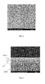
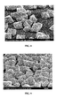
- 238000001878 scanning electron micrograph Methods 0.000 description 20
- 238000000137 annealing Methods 0.000 description 16
- UHOVQNZJYSORNB-UHFFFAOYSA-N Benzene Chemical compound C1=CC=CC=C1 UHOVQNZJYSORNB-UHFFFAOYSA-N 0.000 description 15
- 229910052751 metal Inorganic materials 0.000 description 15
- 230000015572 biosynthetic process Effects 0.000 description 14
- 150000002431 hydrogen Chemical class 0.000 description 14
- 239000002184 metal Substances 0.000 description 14
- 239000010410 layer Substances 0.000 description 13
- YXFVVABEGXRONW-UHFFFAOYSA-N Toluene Chemical compound CC1=CC=CC=C1 YXFVVABEGXRONW-UHFFFAOYSA-N 0.000 description 12
- VLKZOEOYAKHREP-UHFFFAOYSA-N n-Hexane Chemical compound CCCCCC VLKZOEOYAKHREP-UHFFFAOYSA-N 0.000 description 12
- 239000000243 solution Substances 0.000 description 12
- 150000001412 amines Chemical class 0.000 description 11
- 125000005842 heteroatom Chemical group 0.000 description 11
- 150000002466 imines Chemical class 0.000 description 11
- 239000012071 phase Substances 0.000 description 11
- 125000006729 (C2-C5) alkenyl group Chemical group 0.000 description 10
- 0 CC(C)[Ge]N(*(C)C)*#C Chemical compound CC(C)[Ge]N(*(C)C)*#C 0.000 description 10
- 125000003118 aryl group Chemical group 0.000 description 10
- 238000010348 incorporation Methods 0.000 description 10
- 125000001424 substituent group Chemical group 0.000 description 10
- 230000000694 effects Effects 0.000 description 9
- 210000002381 plasma Anatomy 0.000 description 9
- 238000003860 storage Methods 0.000 description 9
- IMNFDUFMRHMDMM-UHFFFAOYSA-N N-Heptane Chemical compound CCCCCCC IMNFDUFMRHMDMM-UHFFFAOYSA-N 0.000 description 8
- OFBQJSOFQDEBGM-UHFFFAOYSA-N Pentane Chemical compound CCCCC OFBQJSOFQDEBGM-UHFFFAOYSA-N 0.000 description 8
- 239000010409 thin film Substances 0.000 description 8
- 150000001335 aliphatic alkanes Chemical class 0.000 description 7
- 150000002429 hydrazines Chemical class 0.000 description 7
- 229910000069 nitrogen hydride Inorganic materials 0.000 description 7
- 238000003786 synthesis reaction Methods 0.000 description 7
- 239000006200 vaporizer Substances 0.000 description 7
- UFHFLCQGNIYNRP-UHFFFAOYSA-N Hydrogen Chemical compound [H][H] UFHFLCQGNIYNRP-UHFFFAOYSA-N 0.000 description 6
- NRTOMJZYCJJWKI-UHFFFAOYSA-N Titanium nitride Chemical compound [Ti]#N NRTOMJZYCJJWKI-UHFFFAOYSA-N 0.000 description 6
- 238000013459 approach Methods 0.000 description 6
- 150000004770 chalcogenides Chemical class 0.000 description 6
- DMBHHRLKUKUOEG-UHFFFAOYSA-N diphenylamine Chemical compound C=1C=CC=CC=1NC1=CC=CC=C1 DMBHHRLKUKUOEG-UHFFFAOYSA-N 0.000 description 6
- 239000007789 gas Substances 0.000 description 6
- 238000004377 microelectronic Methods 0.000 description 6
- 239000012808 vapor phase Substances 0.000 description 6
- NLZUEZXRPGMBCV-UHFFFAOYSA-N Butylhydroxytoluene Chemical compound CC1=CC(C(C)(C)C)=C(O)C(C(C)(C)C)=C1 NLZUEZXRPGMBCV-UHFFFAOYSA-N 0.000 description 5
- 150000001336 alkenes Chemical class 0.000 description 5
- 150000001345 alkine derivatives Chemical class 0.000 description 5
- 238000002425 crystallisation Methods 0.000 description 5
- 230000008025 crystallization Effects 0.000 description 5
- 239000006185 dispersion Substances 0.000 description 5
- 238000002156 mixing Methods 0.000 description 5
- 239000012299 nitrogen atmosphere Substances 0.000 description 5
- 125000000962 organic group Chemical group 0.000 description 5
- 230000007420 reactivation Effects 0.000 description 5
- 239000000725 suspension Substances 0.000 description 5
- JUJWROOIHBZHMG-UHFFFAOYSA-N Pyridine Chemical compound C1=CC=NC=C1 JUJWROOIHBZHMG-UHFFFAOYSA-N 0.000 description 4
- VYPSYNLAJGMNEJ-UHFFFAOYSA-N Silicium dioxide Chemical compound O=[Si]=O VYPSYNLAJGMNEJ-UHFFFAOYSA-N 0.000 description 4
- RMRFFCXPLWYOOY-UHFFFAOYSA-N allyl radical Chemical compound [CH2]C=C RMRFFCXPLWYOOY-UHFFFAOYSA-N 0.000 description 4
- 238000000354 decomposition reaction Methods 0.000 description 4
- 230000008030 elimination Effects 0.000 description 4
- 238000003379 elimination reaction Methods 0.000 description 4
- 150000002170 ethers Chemical class 0.000 description 4
- CBOQJANXLMLOSS-UHFFFAOYSA-N ethyl vanillin Chemical compound CCOC1=CC(C=O)=CC=C1O CBOQJANXLMLOSS-UHFFFAOYSA-N 0.000 description 4
- QUZPNFFHZPRKJD-UHFFFAOYSA-N germane Chemical compound [GeH4] QUZPNFFHZPRKJD-UHFFFAOYSA-N 0.000 description 4
- 229910052986 germanium hydride Inorganic materials 0.000 description 4
- 125000001449 isopropyl group Chemical group [H]C([H])([H])C([H])(*)C([H])([H])[H] 0.000 description 4
- 125000000654 isopropylidene group Chemical group C(C)(C)=* 0.000 description 4
- 238000000655 nuclear magnetic resonance spectrum Methods 0.000 description 4
- TVMXDCGIABBOFY-UHFFFAOYSA-N octane Chemical compound CCCCCCCC TVMXDCGIABBOFY-UHFFFAOYSA-N 0.000 description 4
- 230000003252 repetitive effect Effects 0.000 description 4
- YBRBMKDOPFTVDT-UHFFFAOYSA-N tert-butylamine Chemical compound CC(C)(C)N YBRBMKDOPFTVDT-UHFFFAOYSA-N 0.000 description 4
- 238000002411 thermogravimetry Methods 0.000 description 4
- 238000009834 vaporization Methods 0.000 description 4
- 230000008016 vaporization Effects 0.000 description 4
- JYEUMXHLPRZUAT-UHFFFAOYSA-N 1,2,3-triazine Chemical compound C1=CN=NN=C1 JYEUMXHLPRZUAT-UHFFFAOYSA-N 0.000 description 3
- 239000004322 Butylated hydroxytoluene Substances 0.000 description 3
- RWSOTUBLDIXVET-UHFFFAOYSA-N Dihydrogen sulfide Chemical compound S RWSOTUBLDIXVET-UHFFFAOYSA-N 0.000 description 3
- 229910018321 SbTe Inorganic materials 0.000 description 3
- 230000002411 adverse Effects 0.000 description 3
- 230000008901 benefit Effects 0.000 description 3
- 229910052794 bromium Inorganic materials 0.000 description 3
- 235000010354 butylated hydroxytoluene Nutrition 0.000 description 3
- 229940095259 butylated hydroxytoluene Drugs 0.000 description 3
- 125000004432 carbon atom Chemical group C* 0.000 description 3
- 239000000460 chlorine Substances 0.000 description 3
- 229910052801 chlorine Inorganic materials 0.000 description 3
- 230000002939 deleterious effect Effects 0.000 description 3
- 229910000037 hydrogen sulfide Inorganic materials 0.000 description 3
- RAXXELZNTBOGNW-UHFFFAOYSA-N imidazole Natural products C1=CNC=N1 RAXXELZNTBOGNW-UHFFFAOYSA-N 0.000 description 3
- 229910052740 iodine Inorganic materials 0.000 description 3
- 125000002496 methyl group Chemical group [H]C([H])([H])* 0.000 description 3
- 238000002161 passivation Methods 0.000 description 3
- 125000001997 phenyl group Chemical group [H]C1=C([H])C([H])=C(*)C([H])=C1[H] 0.000 description 3
- 230000009467 reduction Effects 0.000 description 3
- 230000002829 reductive effect Effects 0.000 description 3
- SPVXKVOXSXTJOY-UHFFFAOYSA-N selane Chemical compound [SeH2] SPVXKVOXSXTJOY-UHFFFAOYSA-N 0.000 description 3
- 229910000058 selane Inorganic materials 0.000 description 3
- 150000004756 silanes Chemical class 0.000 description 3
- 238000001947 vapour-phase growth Methods 0.000 description 3
- 125000004209 (C1-C8) alkyl group Chemical group 0.000 description 2
- RYHBNJHYFVUHQT-UHFFFAOYSA-N 1,4-Dioxane Chemical compound C1COCCO1 RYHBNJHYFVUHQT-UHFFFAOYSA-N 0.000 description 2
- NXXYKOUNUYWIHA-UHFFFAOYSA-N 2,6-Dimethylphenol Chemical compound CC1=CC=CC(C)=C1O NXXYKOUNUYWIHA-UHFFFAOYSA-N 0.000 description 2
- UFFBMTHBGFGIHF-UHFFFAOYSA-N 2,6-dimethylaniline Chemical compound CC1=CC=CC(C)=C1N UFFBMTHBGFGIHF-UHFFFAOYSA-N 0.000 description 2
- XOUQAVYLRNOXDO-UHFFFAOYSA-N 2-tert-butyl-5-methylphenol Chemical compound CC1=CC=C(C(C)(C)C)C(O)=C1 XOUQAVYLRNOXDO-UHFFFAOYSA-N 0.000 description 2
- ZCYVEMRRCGMTRW-UHFFFAOYSA-N 7553-56-2 Chemical compound [I] ZCYVEMRRCGMTRW-UHFFFAOYSA-N 0.000 description 2
- WKBOTKDWSSQWDR-UHFFFAOYSA-N Bromine atom Chemical compound [Br] WKBOTKDWSSQWDR-UHFFFAOYSA-N 0.000 description 2
- ZAMOUSCENKQFHK-UHFFFAOYSA-N Chlorine atom Chemical compound [Cl] ZAMOUSCENKQFHK-UHFFFAOYSA-N 0.000 description 2
- YNQLUTRBYVCPMQ-UHFFFAOYSA-N Ethylbenzene Chemical compound CCC1=CC=CC=C1 YNQLUTRBYVCPMQ-UHFFFAOYSA-N 0.000 description 2
- PXGOKWXKJXAPGV-UHFFFAOYSA-N Fluorine Chemical compound FF PXGOKWXKJXAPGV-UHFFFAOYSA-N 0.000 description 2
- YLQBMQCUIZJEEH-UHFFFAOYSA-N Furan Chemical compound C=1C=COC=1 YLQBMQCUIZJEEH-UHFFFAOYSA-N 0.000 description 2
- 239000007818 Grignard reagent Substances 0.000 description 2
- QIGBRXMKCJKVMJ-UHFFFAOYSA-N Hydroquinone Chemical compound OC1=CC=C(O)C=C1 QIGBRXMKCJKVMJ-UHFFFAOYSA-N 0.000 description 2
- SIKJAQJRHWYJAI-UHFFFAOYSA-N Indole Chemical compound C1=CC=C2NC=CC2=C1 SIKJAQJRHWYJAI-UHFFFAOYSA-N 0.000 description 2
- KWYHDKDOAIKMQN-UHFFFAOYSA-N N,N,N',N'-tetramethylethylenediamine Chemical compound CN(C)CCN(C)C KWYHDKDOAIKMQN-UHFFFAOYSA-N 0.000 description 2
- AFBPFSWMIHJQDM-UHFFFAOYSA-N N-methylaniline Chemical compound CNC1=CC=CC=C1 AFBPFSWMIHJQDM-UHFFFAOYSA-N 0.000 description 2
- 206010034972 Photosensitivity reaction Diseases 0.000 description 2
- KAESVJOAVNADME-UHFFFAOYSA-N Pyrrole Chemical compound C=1C=CNC=1 KAESVJOAVNADME-UHFFFAOYSA-N 0.000 description 2
- YTPLMLYBLZKORZ-UHFFFAOYSA-N Thiophene Chemical compound C=1C=CSC=1 YTPLMLYBLZKORZ-UHFFFAOYSA-N 0.000 description 2
- 239000003463 adsorbent Substances 0.000 description 2
- 150000001408 amides Chemical group 0.000 description 2
- RDOXTESZEPMUJZ-UHFFFAOYSA-N anisole Chemical compound COC1=CC=CC=C1 RDOXTESZEPMUJZ-UHFFFAOYSA-N 0.000 description 2
- 150000001462 antimony Chemical class 0.000 description 2
- 239000012298 atmosphere Substances 0.000 description 2
- QVGXLLKOCUKJST-UHFFFAOYSA-N atomic oxygen Chemical compound [O] QVGXLLKOCUKJST-UHFFFAOYSA-N 0.000 description 2
- 239000002585 base Substances 0.000 description 2
- GDTBXPJZTBHREO-UHFFFAOYSA-N bromine Substances BrBr GDTBXPJZTBHREO-UHFFFAOYSA-N 0.000 description 2
- 125000003178 carboxy group Chemical group [H]OC(*)=O 0.000 description 2
- 239000012159 carrier gas Substances 0.000 description 2
- 239000003638 chemical reducing agent Substances 0.000 description 2
- 238000005859 coupling reaction Methods 0.000 description 2
- 150000004985 diamines Chemical class 0.000 description 2
- 125000001495 ethyl group Chemical group [H]C([H])([H])C([H])([H])* 0.000 description 2
- 229940073505 ethyl vanillin Drugs 0.000 description 2
- 239000011737 fluorine Substances 0.000 description 2
- 229910052731 fluorine Inorganic materials 0.000 description 2
- 230000006870 function Effects 0.000 description 2
- 150000002290 germanium Chemical class 0.000 description 2
- 150000002291 germanium compounds Chemical class 0.000 description 2
- 125000005843 halogen group Chemical group 0.000 description 2
- 238000011065 in-situ storage Methods 0.000 description 2
- 239000011630 iodine Substances 0.000 description 2
- 239000002608 ionic liquid Substances 0.000 description 2
- 229910052744 lithium Inorganic materials 0.000 description 2
- 229910003002 lithium salt Inorganic materials 0.000 description 2
- 159000000002 lithium salts Chemical class 0.000 description 2
- VNWKTOKETHGBQD-UHFFFAOYSA-N methane Chemical compound C VNWKTOKETHGBQD-UHFFFAOYSA-N 0.000 description 2
- 238000012986 modification Methods 0.000 description 2
- 230000004048 modification Effects 0.000 description 2
- HVOYZOQVDYHUPF-UHFFFAOYSA-N n,n',n'-trimethylethane-1,2-diamine Chemical compound CNCCN(C)C HVOYZOQVDYHUPF-UHFFFAOYSA-N 0.000 description 2
- 125000001624 naphthyl group Chemical group 0.000 description 2
- QJGQUHMNIGDVPM-UHFFFAOYSA-N nitrogen group Chemical group [N] QJGQUHMNIGDVPM-UHFFFAOYSA-N 0.000 description 2
- 230000006911 nucleation Effects 0.000 description 2
- 238000010899 nucleation Methods 0.000 description 2
- 239000003921 oil Substances 0.000 description 2
- 125000000082 organogermanium group Chemical group 0.000 description 2
- 230000001590 oxidative effect Effects 0.000 description 2
- 239000001301 oxygen Substances 0.000 description 2
- 238000004806 packaging method and process Methods 0.000 description 2
- 125000001147 pentyl group Chemical group C(CCCC)* 0.000 description 2
- 230000036211 photosensitivity Effects 0.000 description 2
- 229920000570 polyether Polymers 0.000 description 2
- 125000002924 primary amino group Chemical group [H]N([H])* 0.000 description 2
- 238000012545 processing Methods 0.000 description 2
- 125000001436 propyl group Chemical group [H]C([*])([H])C([H])([H])C([H])([H])[H] 0.000 description 2
- UMJSCPRVCHMLSP-UHFFFAOYSA-N pyridine Natural products COC1=CC=CN=C1 UMJSCPRVCHMLSP-UHFFFAOYSA-N 0.000 description 2
- 239000004065 semiconductor Substances 0.000 description 2
- 239000000377 silicon dioxide Substances 0.000 description 2
- 239000007790 solid phase Substances 0.000 description 2
- 230000006641 stabilisation Effects 0.000 description 2
- 238000011105 stabilization Methods 0.000 description 2
- 239000007858 starting material Substances 0.000 description 2
- 230000001629 suppression Effects 0.000 description 2
- 238000004381 surface treatment Methods 0.000 description 2
- IEXRMSFAVATTJX-UHFFFAOYSA-N tetrachlorogermane Chemical compound Cl[Ge](Cl)(Cl)Cl IEXRMSFAVATTJX-UHFFFAOYSA-N 0.000 description 2
- 238000002076 thermal analysis method Methods 0.000 description 2
- XLYOFNOQVPJJNP-UHFFFAOYSA-N water Chemical compound O XLYOFNOQVPJJNP-UHFFFAOYSA-N 0.000 description 2
- 229910001868 water Inorganic materials 0.000 description 2
- 239000008096 xylene Substances 0.000 description 2
- KYVBNYUBXIEUFW-UHFFFAOYSA-N 1,1,3,3-tetramethylguanidine Chemical compound CN(C)C(=N)N(C)C KYVBNYUBXIEUFW-UHFFFAOYSA-N 0.000 description 1
- WCBPJVKVIMMEQC-UHFFFAOYSA-N 1,1-diphenyl-2-(2,4,6-trinitrophenyl)hydrazine Chemical group [O-][N+](=O)C1=CC([N+](=O)[O-])=CC([N+]([O-])=O)=C1NN(C=1C=CC=CC=1)C1=CC=CC=C1 WCBPJVKVIMMEQC-UHFFFAOYSA-N 0.000 description 1
- BVOMRRWJQOJMPA-UHFFFAOYSA-N 1,2,3-trithiane Chemical compound C1CSSSC1 BVOMRRWJQOJMPA-UHFFFAOYSA-N 0.000 description 1
- CXWGKAYMVASWDQ-UHFFFAOYSA-N 1,2-dithiane Chemical compound C1CCSSC1 CXWGKAYMVASWDQ-UHFFFAOYSA-N 0.000 description 1
- QBPPRVHXOZRESW-UHFFFAOYSA-N 1,4,7,10-tetraazacyclododecane Chemical compound C1CNCCNCCNCCN1 QBPPRVHXOZRESW-UHFFFAOYSA-N 0.000 description 1
- ITWBWJFEJCHKSN-UHFFFAOYSA-N 1,4,7-triazonane Chemical compound C1CNCCNCCN1 ITWBWJFEJCHKSN-UHFFFAOYSA-N 0.000 description 1
- VQFZKDXSJZVGDA-UHFFFAOYSA-N 1,5,9-triazacyclododecane Chemical compound C1CNCCCNCCCNC1 VQFZKDXSJZVGDA-UHFFFAOYSA-N 0.000 description 1
- KGRVJHAUYBGFFP-UHFFFAOYSA-N 2,2'-Methylenebis(4-methyl-6-tert-butylphenol) Chemical compound CC(C)(C)C1=CC(C)=CC(CC=2C(=C(C=C(C)C=2)C(C)(C)C)O)=C1O KGRVJHAUYBGFFP-UHFFFAOYSA-N 0.000 description 1
- ZFFMLCVRJBZUDZ-UHFFFAOYSA-N 2,3-dimethylbutane Chemical group CC(C)C(C)C ZFFMLCVRJBZUDZ-UHFFFAOYSA-N 0.000 description 1
- IMOYOUMVYICGCA-UHFFFAOYSA-N 2-tert-butyl-4-hydroxyanisole Chemical compound COC1=CC=C(O)C=C1C(C)(C)C IMOYOUMVYICGCA-UHFFFAOYSA-N 0.000 description 1
- MGADZUXDNSDTHW-UHFFFAOYSA-N 2H-pyran Chemical compound C1OC=CC=C1 MGADZUXDNSDTHW-UHFFFAOYSA-N 0.000 description 1
- BCHZICNRHXRCHY-UHFFFAOYSA-N 2h-oxazine Chemical compound N1OC=CC=C1 BCHZICNRHXRCHY-UHFFFAOYSA-N 0.000 description 1
- PZRWFKGUFWPFID-UHFFFAOYSA-N 3,9-dioctadecoxy-2,4,8,10-tetraoxa-3,9-diphosphaspiro[5.5]undecane Chemical compound C1OP(OCCCCCCCCCCCCCCCCCC)OCC21COP(OCCCCCCCCCCCCCCCCCC)OC2 PZRWFKGUFWPFID-UHFFFAOYSA-N 0.000 description 1
- MRBKEAMVRSLQPH-UHFFFAOYSA-N 3-tert-butyl-4-hydroxyanisole Chemical compound COC1=CC=C(O)C(C(C)(C)C)=C1 MRBKEAMVRSLQPH-UHFFFAOYSA-N 0.000 description 1
- UDBVWWVWSXSLAX-UHFFFAOYSA-N 4-[2,3-bis(5-tert-butyl-4-hydroxy-2-methylphenyl)butyl]-2-tert-butyl-5-methylphenol Chemical compound C=1C(C(C)(C)C)=C(O)C=C(C)C=1C(C)C(C=1C(=CC(O)=C(C=1)C(C)(C)C)C)CC1=CC(C(C)(C)C)=C(O)C=C1C UDBVWWVWSXSLAX-UHFFFAOYSA-N 0.000 description 1
- JTTMYKSFKOOQLP-UHFFFAOYSA-N 4-hydroxydiphenylamine Chemical compound C1=CC(O)=CC=C1NC1=CC=CC=C1 JTTMYKSFKOOQLP-UHFFFAOYSA-N 0.000 description 1
- XESZUVZBAMCAEJ-UHFFFAOYSA-N 4-tert-butylcatechol Chemical compound CC(C)(C)C1=CC=C(O)C(O)=C1 XESZUVZBAMCAEJ-UHFFFAOYSA-N 0.000 description 1
- QGZKDVFQNNGYKY-UHFFFAOYSA-O Ammonium Chemical compound [NH4+] QGZKDVFQNNGYKY-UHFFFAOYSA-O 0.000 description 1
- SNRUBQQJIBEYMU-UHFFFAOYSA-N Dodecane Natural products CCCCCCCCCCCC SNRUBQQJIBEYMU-UHFFFAOYSA-N 0.000 description 1
- 229940123457 Free radical scavenger Drugs 0.000 description 1
- 229910000927 Ge alloy Inorganic materials 0.000 description 1
- 229910006109 GeBr4 Inorganic materials 0.000 description 1
- 229910006113 GeCl4 Inorganic materials 0.000 description 1
- WHXSMMKQMYFTQS-UHFFFAOYSA-N Lithium Chemical compound [Li] WHXSMMKQMYFTQS-UHFFFAOYSA-N 0.000 description 1
- UTGQNNCQYDRXCH-UHFFFAOYSA-N N,N'-diphenyl-1,4-phenylenediamine Chemical compound C=1C=C(NC=2C=CC=CC=2)C=CC=1NC1=CC=CC=C1 UTGQNNCQYDRXCH-UHFFFAOYSA-N 0.000 description 1
- CTQNGGLPUBDAKN-UHFFFAOYSA-N O-Xylene Chemical compound CC1=CC=CC=C1C CTQNGGLPUBDAKN-UHFFFAOYSA-N 0.000 description 1
- ZCQWOFVYLHDMMC-UHFFFAOYSA-N Oxazole Chemical compound C1=COC=N1 ZCQWOFVYLHDMMC-UHFFFAOYSA-N 0.000 description 1
- CBENFWSGALASAD-UHFFFAOYSA-N Ozone Chemical compound [O-][O+]=O CBENFWSGALASAD-UHFFFAOYSA-N 0.000 description 1
- ISWSIDIOOBJBQZ-UHFFFAOYSA-N Phenol Chemical compound OC1=CC=CC=C1 ISWSIDIOOBJBQZ-UHFFFAOYSA-N 0.000 description 1
- 229910001245 Sb alloy Inorganic materials 0.000 description 1
- 229910017629 Sb2Te3 Inorganic materials 0.000 description 1
- NINIDFKCEFEMDL-UHFFFAOYSA-N Sulfur Chemical group [S] NINIDFKCEFEMDL-UHFFFAOYSA-N 0.000 description 1
- UCKMPCXJQFINFW-UHFFFAOYSA-N Sulphide Chemical compound [S-2] UCKMPCXJQFINFW-UHFFFAOYSA-N 0.000 description 1
- QYTDEUPAUMOIOP-UHFFFAOYSA-N TEMPO Chemical group CC1(C)CCCC(C)(C)N1[O] QYTDEUPAUMOIOP-UHFFFAOYSA-N 0.000 description 1
- 229910001215 Te alloy Inorganic materials 0.000 description 1
- BGNXCDMCOKJUMV-UHFFFAOYSA-N Tert-Butylhydroquinone Chemical compound CC(C)(C)C1=CC(O)=CC=C1O BGNXCDMCOKJUMV-UHFFFAOYSA-N 0.000 description 1
- FZWLAAWBMGSTSO-UHFFFAOYSA-N Thiazole Chemical compound C1=CSC=N1 FZWLAAWBMGSTSO-UHFFFAOYSA-N 0.000 description 1
- XSQUKJJJFZCRTK-UHFFFAOYSA-N Urea Chemical compound NC(N)=O XSQUKJJJFZCRTK-UHFFFAOYSA-N 0.000 description 1
- BGYHLZZASRKEJE-UHFFFAOYSA-N [3-[3-(3,5-ditert-butyl-4-hydroxyphenyl)propanoyloxy]-2,2-bis[3-(3,5-ditert-butyl-4-hydroxyphenyl)propanoyloxymethyl]propyl] 3-(3,5-ditert-butyl-4-hydroxyphenyl)propanoate Chemical compound CC(C)(C)C1=C(O)C(C(C)(C)C)=CC(CCC(=O)OCC(COC(=O)CCC=2C=C(C(O)=C(C=2)C(C)(C)C)C(C)(C)C)(COC(=O)CCC=2C=C(C(O)=C(C=2)C(C)(C)C)C(C)(C)C)COC(=O)CCC=2C=C(C(O)=C(C=2)C(C)(C)C)C(C)(C)C)=C1 BGYHLZZASRKEJE-UHFFFAOYSA-N 0.000 description 1
- KFMLSKLCIQLEQK-UHFFFAOYSA-N [SiH3].[Sb] Chemical compound [SiH3].[Sb] KFMLSKLCIQLEQK-UHFFFAOYSA-N 0.000 description 1
- 238000000277 atomic layer chemical vapour deposition Methods 0.000 description 1
- 230000002238 attenuated effect Effects 0.000 description 1
- 150000001555 benzenes Chemical class 0.000 description 1
- 125000001797 benzyl group Chemical group [H]C1=C([H])C([H])=C(C([H])=C1[H])C([H])([H])* 0.000 description 1
- 229910052797 bismuth Inorganic materials 0.000 description 1
- SNCZNSNPXMPCGN-UHFFFAOYSA-N butanediamide Chemical compound NC(=O)CCC(N)=O SNCZNSNPXMPCGN-UHFFFAOYSA-N 0.000 description 1
- 239000004202 carbamide Substances 0.000 description 1
- 125000002837 carbocyclic group Chemical group 0.000 description 1
- 230000003197 catalytic effect Effects 0.000 description 1
- 150000001768 cations Chemical class 0.000 description 1
- 210000004027 cell Anatomy 0.000 description 1
- 229910052798 chalcogen Inorganic materials 0.000 description 1
- 150000001787 chalcogens Chemical class 0.000 description 1
- 239000011248 coating agent Substances 0.000 description 1
- 238000000576 coating method Methods 0.000 description 1
- 229910052681 coesite Inorganic materials 0.000 description 1
- 230000008878 coupling Effects 0.000 description 1
- 238000010168 coupling process Methods 0.000 description 1
- 229910052906 cristobalite Inorganic materials 0.000 description 1
- 150000003983 crown ethers Chemical class 0.000 description 1
- 125000004122 cyclic group Chemical group 0.000 description 1
- 125000001995 cyclobutyl group Chemical group [H]C1([H])C([H])([H])C([H])(*)C1([H])[H] 0.000 description 1
- 125000000113 cyclohexyl group Chemical group [H]C1([H])C([H])([H])C([H])([H])C([H])(*)C([H])([H])C1([H])[H] 0.000 description 1
- 125000001511 cyclopentyl group Chemical group [H]C1([H])C([H])([H])C([H])([H])C([H])(*)C1([H])[H] 0.000 description 1
- 125000001559 cyclopropyl group Chemical group [H]C1([H])C([H])([H])C1([H])* 0.000 description 1
- 230000007423 decrease Effects 0.000 description 1
- 125000002704 decyl group Chemical group [H]C([H])([H])C([H])([H])C([H])([H])C([H])([H])C([H])([H])C([H])([H])C([H])([H])C([H])([H])C([H])([H])C([H])([H])* 0.000 description 1
- 238000003795 desorption Methods 0.000 description 1
- 230000001627 detrimental effect Effects 0.000 description 1
- 238000011161 development Methods 0.000 description 1
- VXGHASBVNMHGDI-UHFFFAOYSA-N digermane Chemical compound [Ge][Ge] VXGHASBVNMHGDI-UHFFFAOYSA-N 0.000 description 1
- LOZWAPSEEHRYPG-UHFFFAOYSA-N dithiane Natural products C1CSCCS1 LOZWAPSEEHRYPG-UHFFFAOYSA-N 0.000 description 1
- 125000003438 dodecyl group Chemical group [H]C([H])([H])C([H])([H])C([H])([H])C([H])([H])C([H])([H])C([H])([H])C([H])([H])C([H])([H])C([H])([H])C([H])([H])C([H])([H])C([H])([H])* 0.000 description 1
- 238000002149 energy-dispersive X-ray emission spectroscopy Methods 0.000 description 1
- 238000000724 energy-dispersive X-ray spectrum Methods 0.000 description 1
- 238000005516 engineering process Methods 0.000 description 1
- LIWAQLJGPBVORC-UHFFFAOYSA-N ethylmethylamine Chemical compound CCNC LIWAQLJGPBVORC-UHFFFAOYSA-N 0.000 description 1
- 230000008020 evaporation Effects 0.000 description 1
- 238000001704 evaporation Methods 0.000 description 1
- 238000002474 experimental method Methods 0.000 description 1
- 238000009472 formulation Methods 0.000 description 1
- ZTHYODDOHIVTJV-UHFFFAOYSA-N gallic acid propyl ester Natural products CCCOC(=O)C1=CC(O)=C(O)C(O)=C1 ZTHYODDOHIVTJV-UHFFFAOYSA-N 0.000 description 1
- 238000004817 gas chromatography Methods 0.000 description 1
- 238000010574 gas phase reaction Methods 0.000 description 1
- 229910000078 germane Inorganic materials 0.000 description 1
- 150000004795 grignard reagents Chemical class 0.000 description 1
- 230000017525 heat dissipation Effects 0.000 description 1
- 238000010438 heat treatment Methods 0.000 description 1
- 125000003187 heptyl group Chemical group [H]C([*])([H])C([H])([H])C([H])([H])C([H])([H])C([H])([H])C([H])([H])C([H])([H])[H] 0.000 description 1
- 125000004051 hexyl group Chemical group [H]C([H])([H])C([H])([H])C([H])([H])C([H])([H])C([H])([H])C([H])([H])* 0.000 description 1
- 150000004678 hydrides Chemical class 0.000 description 1
- 125000001145 hydrido group Chemical class *[H] 0.000 description 1
- 229930195733 hydrocarbon Natural products 0.000 description 1
- 150000002430 hydrocarbons Chemical class 0.000 description 1
- 229960004337 hydroquinone Drugs 0.000 description 1
- 150000002460 imidazoles Chemical class 0.000 description 1
- 238000011534 incubation Methods 0.000 description 1
- PZOUSPYUWWUPPK-UHFFFAOYSA-N indole Natural products CC1=CC=CC2=C1C=CN2 PZOUSPYUWWUPPK-UHFFFAOYSA-N 0.000 description 1
- RKJUIXBNRJVNHR-UHFFFAOYSA-N indolenine Natural products C1=CC=C2CC=NC2=C1 RKJUIXBNRJVNHR-UHFFFAOYSA-N 0.000 description 1
- 150000002475 indoles Chemical class 0.000 description 1
- 230000000977 initiatory effect Effects 0.000 description 1
- 238000002347 injection Methods 0.000 description 1
- 239000007924 injection Substances 0.000 description 1
- 230000003993 interaction Effects 0.000 description 1
- 230000002452 interceptive effect Effects 0.000 description 1
- 125000001972 isopentyl group Chemical group [H]C([H])([H])C([H])(C([H])([H])[H])C([H])([H])C([H])([H])* 0.000 description 1
- 238000005304 joining Methods 0.000 description 1
- 239000012705 liquid precursor Substances 0.000 description 1
- 239000006193 liquid solution Substances 0.000 description 1
- 150000002739 metals Chemical class 0.000 description 1
- UZKWTJUDCOPSNM-UHFFFAOYSA-N methoxybenzene Substances CCCCOC=C UZKWTJUDCOPSNM-UHFFFAOYSA-N 0.000 description 1
- 238000001000 micrograph Methods 0.000 description 1
- GTIBACHAUHDNPH-WHYMJUELSA-N n,n'-bis[(z)-benzylideneamino]oxamide Chemical compound C=1C=CC=CC=1\C=N/NC(=O)C(=O)N\N=C/C1=CC=CC=C1 GTIBACHAUHDNPH-WHYMJUELSA-N 0.000 description 1
- ZUSRFDBQZSPBDV-UHFFFAOYSA-N n-[bis(dimethylamino)stibanyl]-n-methylmethanamine Chemical compound CN(C)[Sb](N(C)C)N(C)C ZUSRFDBQZSPBDV-UHFFFAOYSA-N 0.000 description 1
- 125000004108 n-butyl group Chemical group [H]C([H])([H])C([H])([H])C([H])([H])C([H])([H])* 0.000 description 1
- JKUUTODNPMRHHZ-UHFFFAOYSA-N n-methyl-n-[tris(dimethylamino)germyl]methanamine Chemical compound CN(C)[Ge](N(C)C)(N(C)C)N(C)C JKUUTODNPMRHHZ-UHFFFAOYSA-N 0.000 description 1
- 125000004433 nitrogen atom Chemical group N* 0.000 description 1
- 125000001400 nonyl group Chemical group [H]C([*])([H])C([H])([H])C([H])([H])C([H])([H])C([H])([H])C([H])([H])C([H])([H])C([H])([H])C([H])([H])[H] 0.000 description 1
- SSDSCDGVMJFTEQ-UHFFFAOYSA-N octadecyl 3-(3,5-ditert-butyl-4-hydroxyphenyl)propanoate Chemical compound CCCCCCCCCCCCCCCCCCOC(=O)CCC1=CC(C(C)(C)C)=C(O)C(C(C)(C)C)=C1 SSDSCDGVMJFTEQ-UHFFFAOYSA-N 0.000 description 1
- 125000002347 octyl group Chemical group [H]C([*])([H])C([H])([H])C([H])([H])C([H])([H])C([H])([H])C([H])([H])C([H])([H])C([H])([H])[H] 0.000 description 1
- 239000003960 organic solvent Substances 0.000 description 1
- 230000003647 oxidation Effects 0.000 description 1
- 238000007254 oxidation reaction Methods 0.000 description 1
- 238000006464 oxidative addition reaction Methods 0.000 description 1
- 230000036961 partial effect Effects 0.000 description 1
- 239000002245 particle Substances 0.000 description 1
- 150000002989 phenols Chemical class 0.000 description 1
- 150000002990 phenothiazines Chemical class 0.000 description 1
- 238000010944 pre-mature reactiony Methods 0.000 description 1
- 238000002360 preparation method Methods 0.000 description 1
- JUJWROOIHBZHMG-RALIUCGRSA-N pyridine-d5 Chemical compound [2H]C1=NC([2H])=C([2H])C([2H])=C1[2H] JUJWROOIHBZHMG-RALIUCGRSA-N 0.000 description 1
- 150000003230 pyrimidines Chemical class 0.000 description 1
- 239000002516 radical scavenger Substances 0.000 description 1
- 230000000717 retained effect Effects 0.000 description 1
- 235000002020 sage Nutrition 0.000 description 1
- 150000003839 salts Chemical class 0.000 description 1
- 238000005201 scrubbing Methods 0.000 description 1
- 125000002914 sec-butyl group Chemical group [H]C([H])([H])C([H])([H])C([H])(*)C([H])([H])[H] 0.000 description 1
- 229910052711 selenium Inorganic materials 0.000 description 1
- 235000012239 silicon dioxide Nutrition 0.000 description 1
- 239000002356 single layer Substances 0.000 description 1
- 238000000935 solvent evaporation Methods 0.000 description 1
- 238000004611 spectroscopical analysis Methods 0.000 description 1
- 238000001228 spectrum Methods 0.000 description 1
- 229910052682 stishovite Inorganic materials 0.000 description 1
- 238000000859 sublimation Methods 0.000 description 1
- 230000008022 sublimation Effects 0.000 description 1
- 239000000126 substance Substances 0.000 description 1
- 125000003107 substituted aryl group Chemical group 0.000 description 1
- BDHFUVZGWQCTTF-UHFFFAOYSA-M sulfonate Chemical compound [O-]S(=O)=O BDHFUVZGWQCTTF-UHFFFAOYSA-M 0.000 description 1
- JBQYATWDVHIOAR-UHFFFAOYSA-N tellanylidenegermanium Chemical compound [Te]=[Ge] JBQYATWDVHIOAR-UHFFFAOYSA-N 0.000 description 1
- 235000019281 tert-butylhydroquinone Nutrition 0.000 description 1
- VJHDVMPJLLGYBL-UHFFFAOYSA-N tetrabromogermane Chemical compound Br[Ge](Br)(Br)Br VJHDVMPJLLGYBL-UHFFFAOYSA-N 0.000 description 1
- QQXSEZVCKAEYQJ-UHFFFAOYSA-N tetraethylgermanium Chemical compound CC[Ge](CC)(CC)CC QQXSEZVCKAEYQJ-UHFFFAOYSA-N 0.000 description 1
- ZRLCXMPFXYVHGS-UHFFFAOYSA-N tetramethylgermane Chemical compound C[Ge](C)(C)C ZRLCXMPFXYVHGS-UHFFFAOYSA-N 0.000 description 1
- CBDKQYKMCICBOF-UHFFFAOYSA-N thiazoline Chemical compound C1CN=CS1 CBDKQYKMCICBOF-UHFFFAOYSA-N 0.000 description 1
- 125000004149 thio group Chemical group *S* 0.000 description 1
- 229930192474 thiophene Natural products 0.000 description 1
- RBEXEKTWBGMBDZ-UHFFFAOYSA-N tri(propan-2-yl)stibane Chemical compound CC(C)[Sb](C(C)C)C(C)C RBEXEKTWBGMBDZ-UHFFFAOYSA-N 0.000 description 1
- 150000003852 triazoles Chemical class 0.000 description 1
- BXJWDOYMROEHEN-UHFFFAOYSA-N tributylstibane Chemical compound CCCC[Sb](CCCC)CCCC BXJWDOYMROEHEN-UHFFFAOYSA-N 0.000 description 1
- 229910052905 tridymite Inorganic materials 0.000 description 1
- RKBCYCFRFCNLTO-UHFFFAOYSA-N triisopropylamine Chemical class CC(C)N(C(C)C)C(C)C RKBCYCFRFCNLTO-UHFFFAOYSA-N 0.000 description 1
- 125000002948 undecyl group Chemical group [H]C([*])([H])C([H])([H])C([H])([H])C([H])([H])C([H])([H])C([H])([H])C([H])([H])C([H])([H])C([H])([H])C([H])([H])C([H])([H])[H] 0.000 description 1
- UIYCHXAGWOYNNA-UHFFFAOYSA-N vinyl sulfide Chemical group C=CSC=C UIYCHXAGWOYNNA-UHFFFAOYSA-N 0.000 description 1
- 150000003738 xylenes Chemical class 0.000 description 1
Images


Classifications
-
- C—CHEMISTRY; METALLURGY
- C07—ORGANIC CHEMISTRY
- C07F—ACYCLIC, CARBOCYCLIC OR HETEROCYCLIC COMPOUNDS CONTAINING ELEMENTS OTHER THAN CARBON, HYDROGEN, HALOGEN, OXYGEN, NITROGEN, SULFUR, SELENIUM OR TELLURIUM
- C07F7/00—Compounds containing elements of Groups 4 or 14 of the Periodic Table
- C07F7/30—Germanium compounds
-
- C—CHEMISTRY; METALLURGY
- C23—COATING METALLIC MATERIAL; COATING MATERIAL WITH METALLIC MATERIAL; CHEMICAL SURFACE TREATMENT; DIFFUSION TREATMENT OF METALLIC MATERIAL; COATING BY VACUUM EVAPORATION, BY SPUTTERING, BY ION IMPLANTATION OR BY CHEMICAL VAPOUR DEPOSITION, IN GENERAL; INHIBITING CORROSION OF METALLIC MATERIAL OR INCRUSTATION IN GENERAL
- C23C—COATING METALLIC MATERIAL; COATING MATERIAL WITH METALLIC MATERIAL; SURFACE TREATMENT OF METALLIC MATERIAL BY DIFFUSION INTO THE SURFACE, BY CHEMICAL CONVERSION OR SUBSTITUTION; COATING BY VACUUM EVAPORATION, BY SPUTTERING, BY ION IMPLANTATION OR BY CHEMICAL VAPOUR DEPOSITION, IN GENERAL
- C23C16/00—Chemical coating by decomposition of gaseous compounds, without leaving reaction products of surface material in the coating, i.e. chemical vapour deposition [CVD] processes
- C23C16/22—Chemical coating by decomposition of gaseous compounds, without leaving reaction products of surface material in the coating, i.e. chemical vapour deposition [CVD] processes characterised by the deposition of inorganic material, other than metallic material
- C23C16/30—Deposition of compounds, mixtures or solid solutions, e.g. borides, carbides, nitrides
- C23C16/305—Sulfides, selenides, or tellurides
-
- C—CHEMISTRY; METALLURGY
- C23—COATING METALLIC MATERIAL; COATING MATERIAL WITH METALLIC MATERIAL; CHEMICAL SURFACE TREATMENT; DIFFUSION TREATMENT OF METALLIC MATERIAL; COATING BY VACUUM EVAPORATION, BY SPUTTERING, BY ION IMPLANTATION OR BY CHEMICAL VAPOUR DEPOSITION, IN GENERAL; INHIBITING CORROSION OF METALLIC MATERIAL OR INCRUSTATION IN GENERAL
- C23C—COATING METALLIC MATERIAL; COATING MATERIAL WITH METALLIC MATERIAL; SURFACE TREATMENT OF METALLIC MATERIAL BY DIFFUSION INTO THE SURFACE, BY CHEMICAL CONVERSION OR SUBSTITUTION; COATING BY VACUUM EVAPORATION, BY SPUTTERING, BY ION IMPLANTATION OR BY CHEMICAL VAPOUR DEPOSITION, IN GENERAL
- C23C16/00—Chemical coating by decomposition of gaseous compounds, without leaving reaction products of surface material in the coating, i.e. chemical vapour deposition [CVD] processes
- C23C16/44—Chemical coating by decomposition of gaseous compounds, without leaving reaction products of surface material in the coating, i.e. chemical vapour deposition [CVD] processes characterised by the method of coating
- C23C16/448—Chemical coating by decomposition of gaseous compounds, without leaving reaction products of surface material in the coating, i.e. chemical vapour deposition [CVD] processes characterised by the method of coating characterised by the method used for generating reactive gas streams, e.g. by evaporation or sublimation of precursor materials
-
- C—CHEMISTRY; METALLURGY
- C23—COATING METALLIC MATERIAL; COATING MATERIAL WITH METALLIC MATERIAL; CHEMICAL SURFACE TREATMENT; DIFFUSION TREATMENT OF METALLIC MATERIAL; COATING BY VACUUM EVAPORATION, BY SPUTTERING, BY ION IMPLANTATION OR BY CHEMICAL VAPOUR DEPOSITION, IN GENERAL; INHIBITING CORROSION OF METALLIC MATERIAL OR INCRUSTATION IN GENERAL
- C23C—COATING METALLIC MATERIAL; COATING MATERIAL WITH METALLIC MATERIAL; SURFACE TREATMENT OF METALLIC MATERIAL BY DIFFUSION INTO THE SURFACE, BY CHEMICAL CONVERSION OR SUBSTITUTION; COATING BY VACUUM EVAPORATION, BY SPUTTERING, BY ION IMPLANTATION OR BY CHEMICAL VAPOUR DEPOSITION, IN GENERAL
- C23C16/00—Chemical coating by decomposition of gaseous compounds, without leaving reaction products of surface material in the coating, i.e. chemical vapour deposition [CVD] processes
- C23C16/44—Chemical coating by decomposition of gaseous compounds, without leaving reaction products of surface material in the coating, i.e. chemical vapour deposition [CVD] processes characterised by the method of coating
- C23C16/455—Chemical coating by decomposition of gaseous compounds, without leaving reaction products of surface material in the coating, i.e. chemical vapour deposition [CVD] processes characterised by the method of coating characterised by the method used for introducing gases into reaction chamber or for modifying gas flows in reaction chamber
- C23C16/45523—Pulsed gas flow or change of composition over time
- C23C16/45525—Atomic layer deposition [ALD]
- C23C16/45527—Atomic layer deposition [ALD] characterized by the ALD cycle, e.g. different flows or temperatures during half-reactions, unusual pulsing sequence, use of precursor mixtures or auxiliary reactants or activations
- C23C16/45534—Use of auxiliary reactants other than used for contributing to the composition of the main film, e.g. catalysts, activators or scavengers
-
- C—CHEMISTRY; METALLURGY
- C23—COATING METALLIC MATERIAL; COATING MATERIAL WITH METALLIC MATERIAL; CHEMICAL SURFACE TREATMENT; DIFFUSION TREATMENT OF METALLIC MATERIAL; COATING BY VACUUM EVAPORATION, BY SPUTTERING, BY ION IMPLANTATION OR BY CHEMICAL VAPOUR DEPOSITION, IN GENERAL; INHIBITING CORROSION OF METALLIC MATERIAL OR INCRUSTATION IN GENERAL
- C23C—COATING METALLIC MATERIAL; COATING MATERIAL WITH METALLIC MATERIAL; SURFACE TREATMENT OF METALLIC MATERIAL BY DIFFUSION INTO THE SURFACE, BY CHEMICAL CONVERSION OR SUBSTITUTION; COATING BY VACUUM EVAPORATION, BY SPUTTERING, BY ION IMPLANTATION OR BY CHEMICAL VAPOUR DEPOSITION, IN GENERAL
- C23C16/00—Chemical coating by decomposition of gaseous compounds, without leaving reaction products of surface material in the coating, i.e. chemical vapour deposition [CVD] processes
- C23C16/44—Chemical coating by decomposition of gaseous compounds, without leaving reaction products of surface material in the coating, i.e. chemical vapour deposition [CVD] processes characterised by the method of coating
- C23C16/455—Chemical coating by decomposition of gaseous compounds, without leaving reaction products of surface material in the coating, i.e. chemical vapour deposition [CVD] processes characterised by the method of coating characterised by the method used for introducing gases into reaction chamber or for modifying gas flows in reaction chamber
- C23C16/45523—Pulsed gas flow or change of composition over time
- C23C16/45525—Atomic layer deposition [ALD]
- C23C16/45527—Atomic layer deposition [ALD] characterized by the ALD cycle, e.g. different flows or temperatures during half-reactions, unusual pulsing sequence, use of precursor mixtures or auxiliary reactants or activations
- C23C16/45536—Use of plasma, radiation or electromagnetic fields
- C23C16/45542—Plasma being used non-continuously during the ALD reactions
-
- C—CHEMISTRY; METALLURGY
- C23—COATING METALLIC MATERIAL; COATING MATERIAL WITH METALLIC MATERIAL; CHEMICAL SURFACE TREATMENT; DIFFUSION TREATMENT OF METALLIC MATERIAL; COATING BY VACUUM EVAPORATION, BY SPUTTERING, BY ION IMPLANTATION OR BY CHEMICAL VAPOUR DEPOSITION, IN GENERAL; INHIBITING CORROSION OF METALLIC MATERIAL OR INCRUSTATION IN GENERAL
- C23C—COATING METALLIC MATERIAL; COATING MATERIAL WITH METALLIC MATERIAL; SURFACE TREATMENT OF METALLIC MATERIAL BY DIFFUSION INTO THE SURFACE, BY CHEMICAL CONVERSION OR SUBSTITUTION; COATING BY VACUUM EVAPORATION, BY SPUTTERING, BY ION IMPLANTATION OR BY CHEMICAL VAPOUR DEPOSITION, IN GENERAL
- C23C16/00—Chemical coating by decomposition of gaseous compounds, without leaving reaction products of surface material in the coating, i.e. chemical vapour deposition [CVD] processes
- C23C16/56—After-treatment
-
- H—ELECTRICITY
- H10—SEMICONDUCTOR DEVICES; ELECTRIC SOLID-STATE DEVICES NOT OTHERWISE PROVIDED FOR
- H10N—ELECTRIC SOLID-STATE DEVICES NOT OTHERWISE PROVIDED FOR
- H10N70/00—Solid-state devices having no potential barriers, and specially adapted for rectifying, amplifying, oscillating or switching
- H10N70/011—Manufacture or treatment of multistable switching devices
- H10N70/021—Formation of switching materials, e.g. deposition of layers
- H10N70/023—Formation of switching materials, e.g. deposition of layers by chemical vapor deposition, e.g. MOCVD, ALD
-
- H—ELECTRICITY
- H10—SEMICONDUCTOR DEVICES; ELECTRIC SOLID-STATE DEVICES NOT OTHERWISE PROVIDED FOR
- H10N—ELECTRIC SOLID-STATE DEVICES NOT OTHERWISE PROVIDED FOR
- H10N70/00—Solid-state devices having no potential barriers, and specially adapted for rectifying, amplifying, oscillating or switching
- H10N70/20—Multistable switching devices, e.g. memristors
- H10N70/231—Multistable switching devices, e.g. memristors based on solid-state phase change, e.g. between amorphous and crystalline phases, Ovshinsky effect
-
- H—ELECTRICITY
- H10—SEMICONDUCTOR DEVICES; ELECTRIC SOLID-STATE DEVICES NOT OTHERWISE PROVIDED FOR
- H10N—ELECTRIC SOLID-STATE DEVICES NOT OTHERWISE PROVIDED FOR
- H10N70/00—Solid-state devices having no potential barriers, and specially adapted for rectifying, amplifying, oscillating or switching
- H10N70/801—Constructional details of multistable switching devices
- H10N70/881—Switching materials
- H10N70/882—Compounds of sulfur, selenium or tellurium, e.g. chalcogenides
- H10N70/8825—Selenides, e.g. GeSe
-
- H—ELECTRICITY
- H10—SEMICONDUCTOR DEVICES; ELECTRIC SOLID-STATE DEVICES NOT OTHERWISE PROVIDED FOR
- H10N—ELECTRIC SOLID-STATE DEVICES NOT OTHERWISE PROVIDED FOR
- H10N70/00—Solid-state devices having no potential barriers, and specially adapted for rectifying, amplifying, oscillating or switching
- H10N70/801—Constructional details of multistable switching devices
- H10N70/881—Switching materials
- H10N70/882—Compounds of sulfur, selenium or tellurium, e.g. chalcogenides
- H10N70/8828—Tellurides, e.g. GeSbTe
-
- Y—GENERAL TAGGING OF NEW TECHNOLOGICAL DEVELOPMENTS; GENERAL TAGGING OF CROSS-SECTIONAL TECHNOLOGIES SPANNING OVER SEVERAL SECTIONS OF THE IPC; TECHNICAL SUBJECTS COVERED BY FORMER USPC CROSS-REFERENCE ART COLLECTIONS [XRACs] AND DIGESTS
- Y10—TECHNICAL SUBJECTS COVERED BY FORMER USPC
- Y10T—TECHNICAL SUBJECTS COVERED BY FORMER US CLASSIFICATION
- Y10T428/00—Stock material or miscellaneous articles
- Y10T428/31504—Composite [nonstructural laminate]
- Y10T428/31678—Of metal
Definitions
- the present invention relates to a chemical vapor deposition process for forming amorphous films including germanium, tellurium and/or antimony on substrates, including, for example, germanium telluride (GeTe) and germanium antimony telluride (GST) films, as well as phase change random access memory devices and other devices incorporating such films.
- the present invention relates to amorphous GeTe and GST films formed from CVD processes, and devices formed from these films.
- PCRAM Phase change random access memory
- ALD atomic layer deposition
- CVD chemical vapor deposition
- germanium and tellurium precursors described herein can be reacted in a reducing environment with ammonia, or, in some embodiments, in a nitrogen atmosphere, at a controlled temperature and pressure, to yield amorphous GeTe.
- the temperature of the deposition is 320°C or less, and the pressure is 8 torr or less. In another embodiment, the temperature is 350°C or less, and the pressure is 0.8 torr or less.
- Deposition of Ge from the germanium precursors is fast at low temperatures.
- Te incorporation requires a relatively high deposition temperature and pressure, which tends to result in the formation of crystalline GeTe.
- an amorphous GeTe film can be attained. This amorphous GeTe film remains relatively smooth after crystallization. This process can also be extended to other dialkyl Te precursors, such as di-isopropyl Te.
- the present invention relates to a process for depositing an amorphous GeTe material on a substrate by chemical vapor deposition from a precursor which is vaporized to form a precursor vapor which is then contacted with the substrate.
- Representative precursors for depositing the amorphous GeTe films include Ge butylamidinate, (GeBAMDN) and [ ⁇ nBuC(iPrN) 2 Ge], also referred to herein as GeM.
- Ge butyl amidinate or GeM ( ⁇ nBuC(iPrN)2 ⁇ 2Ge) have been developed, together with t-butyl Te, to yield amorphous GeTe at 320°C and 8 torr pressure, and 350°C at 0.8 torr pressure with ammonia co-reactant.
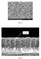
- a process for crystallizing an amorphous GeTe film to yield a relatively smooth GeTe film is described. While deposition of Ge from Ge amidinate or GeM is fast at low temperatures, incorporation of Te requires a relatively high deposition temperature and pressure, which tends to result in the formation of crystalline GeTe. Crystalline GeTe yields a thin film that is not smooth. By controlling both the temperature and pressure, an amorphous GeTe film can be attained. The amorphous GeTe film remains relatively smooth after crystallization.
- this process can also be extended to other dialkyl Te precursors, such as di-isopropyl Te.
- the invention relates to a method of forming a GeTe, GST, antimony, or other such film on a substrate, said method comprising volatilizing a germanium, antimony, or tellurium precursor described herein to form a precursor vapor, and contacting such precursor vapor with a substrate to form the germanium-, antimony-, and/or tellurium-containing film thereon.
- the invention relates to a precursor composition for forming a germanium-containing film, comprising [ ⁇ nBuC(iPrN) 2 ⁇ 2 Ge], also referred to herein as GeM.
- Another aspect of the invention relates to a smooth amorphous germanium telluride or germanium-antimony-telluride film.
- a further aspect of the invention relates to a method of forming a smooth amorphous germanium telluride film, comprising volatilizing [ ⁇ nBuC(iPrN) 2 ⁇ 2 Ge] and a diakyl tellurium precursor to form a precursor vapor and contacting the precursor vapor with a substrate to form the smooth amorphous germanium telluride film on the substrate.
- the invention in another aspect, relates to a method of forming a phase change random access memory device, comprising forming a germanium telluride film of amorphous character, comprising chemical vapor deposition of germanium from a germanium precursor comprising [ ⁇ nBuC(iPrN) 2 ⁇ 2 Ge] or Ge butylamidinate.
- the invention in another aspect relates to a method of making a PCRAM device, comprising forming a GeTe or GST film on a substrate for fabrication of said device, wherein said forming comprises depositing a film layer on the substrate from the vapor of a precursor described herein, using the processes for depositing amorphous germanium, tellurium, and or antimony layers described herein.
- the precursors can be used to form a GST film on a substrate, by depositing one or more of the antimony-containing precursors described herein along with one or more germanium and tellurium-containing precursors on the substrate from a vapor comprising the precursors.
- the precursors can also be used to form PCRAM devices, by forming a GST film on a substrate for fabrication of said device as described above.
- the invention relates to a method of combating pre-reaction of the precursors described herein in a vapor deposition process for forming a film on a substrate, wherein the precursor is susceptible to pre-reaction adversely affecting the film, said method comprising introducing to said process a pre-reaction-combating agent selected from the group consisting of (i) heteroatom (O, N, S) organo Lewis base compounds, (ii) free radical inhibitors, and (iii) deuterium-containing reagents.
- a pre-reaction-combating agent selected from the group consisting of (i) heteroatom (O, N, S) organo Lewis base compounds, (ii) free radical inhibitors, and (iii) deuterium-containing reagents.
- Another aspect of the invention relates to a method of combating pre-reaction of the precursors described herein in a vapor deposition process in which multiple feed streams are flowed to a deposition locus to form a film on a substrate, wherein at least one of said multiple feed streams includes a precursor susceptible to pre-reaction adversely affecting the film, said method comprising introducing to at least one of said multiple feed streams or supplied materials therefor, or to the deposition locus, a pre-reaction-combating agent selected from the group consisting of (i) heteroatom (O, N, S) organo Lewis base compounds, (ii) free radical inhibitors, and (iii) deuterium-containing reagents.
- a pre-reaction-combating agent selected from the group consisting of (i) heteroatom (O, N, S) organo Lewis base compounds, (ii) free radical inhibitors, and (iii) deuterium-containing reagents.
- a still further aspect of the invention relates to a composition, comprising a precursor and a pre-reaction-combating agent for said precursor, said pre-reaction-combating agent being selected from the group consisting of (i) heteroatom (O, N, S) organo Lewis base compounds, (ii) free radical inhibitors, and (iii) deuterium-containing reagents.
- the invention relates to a method of combating pre-reaction of a vapor phase precursor as described herein in contact with a substrate for deposition of a film component thereon, comprising contacting said substrate, prior to said contact of the vapor phase precursor therewith, with a pre-reaction-combating agent selected from the group consisting of (i) heteroatom (O, N, S) organo Lewis base compounds, (ii) free radical inhibitors, and (iii) deuterium-containing reagents.
- a pre-reaction-combating agent selected from the group consisting of (i) heteroatom (O, N, S) organo Lewis base compounds, (ii) free radical inhibitors, and (iii) deuterium-containing reagents.
- the invention relates to a process wherein the pre-reaction combating reagent is introduced to passivate the surface of a growing film or slow the deposition rate, followed by reactivation using an alternative precursor or co-reactant (for example H 2 , NH 3 , plasma, H 2 O hydrogen sulfide, hydrogen selenide, diorganotellurides, diorganosulfides, diorganoselenides, etc.).
- an alternative precursor or co-reactant for example H 2 , NH 3 , plasma, H 2 O hydrogen sulfide, hydrogen selenide, diorganotellurides, diorganosulfides, diorganoselenides, etc.
- Prereaction-combating agents can be selected from the group consisting of (i) heteroatom (O, N, S) organo Lewis base compounds, (ii) free radical inhibitors, and (iii) deuterium-containing reagents.
- Another aspect of the invention relates to a vapor phase deposition process for forming a film on a substrate involving cyclic contacting of the substrate with at least one film precursor described herein that is undesirably pre-reactive in the vapor phase, such process comprising introducing to said film during growth thereof a pre-reaction-combating reagent that is effective to passivate a surface of said film or to slow rate of deposition of said film precursor, and after introducing said pre-reaction-combating reagent, reactivating said film with a different film precursor.
- the invention relates in a further aspect to a method of forming a germanium-containing film on a substrate by a vapor deposition process, comprising volatilizing a germanium precursor to form a germanium precursor vapor, optionally combining the precursor vapor with a component selected from the group consisting of ammonia, hydrogen, helium, argon, and nitrogen, and contacting the precursor vapor with a substrate for vapor deposition of the germanium-containing film thereon, wherein the germanium precursor is selected from the group consisting of the following germanium compositions: wherein:
- Another aspect of the invention relates to a germanium precursor, selected from the group consisting of the above-specified germanium precursor species.
- a still further aspect of the invention relates to a smooth amorphous germanium telluride or germanium antimony telluride film, as formed by the method described above, using a germanium precursor comprising Ge butylamidinate or [ ⁇ nBuC(iPrN) 2 ⁇ 2 Ge].
- the present invention relates to the use of various germanium, tellurium, and antimony precursors, having utility for forming highly conformal germanium-containing films by low temperature ( ⁇ 300°C) vapor deposition processes such as CVD and ALD, in methods for forming germanium-containing films.
- the invention relates to films formed using the methods, and microelectronic device products incorporating such films.
- germanium-containing films such as films of GeTe, GST, and the like.
- the GeTe films can be GexTel-x systems, as such are defined in Scharnhorst and Riedl, "Photoconductivity in the amorphous Ge-rich GexTe1-x system," Journal of Applied Physics, Vol.
- film refers to a layer of deposited material having a thickness below 1000 micrometers, e.g., from such value down to atomic monolayer thickness values.
- film thicknesses of deposited material layers in the practice of the invention may for example be below 100, 10, or 1 micrometers, or in various thin film regimes below 200, 100, or 50 nanometers, depending on the specific application involved.
- the term “thin film” means a layer of a material having a thickness below 1 micrometer.
- a carbon number range e.g., in C 1 -C 12 alkyl
- identification of a carbon number range is intended to include each of the component carbon number moieties within such range, so that each intervening carbon number and any other stated or intervening carbon number value in that stated range, is encompassed, it being further understood that sub-ranges of carbon number within specified carbon number ranges may independently be included in smaller carbon number ranges, within the scope of the invention, and that ranges of carbon numbers specifically excluding a carbon number or numbers are included in the invention, and sub-ranges excluding either or both of carbon number limits of specified ranges are also included in the invention.
- C 1 -C 12 alkyl is intended to include methyl, ethyl, propyl, butyl, pentyl, hexyl, heptyl, octyl, nonyl, decyl, undecyl and dodecyl, including straight chain as well as branched groups of such types. It therefore is to be appreciated that identification of a carbon number range, e.g., C 1 -C 12 , as broadly applicable to a substituent moiety, enables, in specific embodiments of the invention, the carbon number range to be further restricted, as a sub-group of moieties having a carbon number range within the broader specification of the substituent moiety.
- the carbon number range e.g., C 1 -C 12 alkyl
- the carbon number range may be more restrictively specified, in particular embodiments of the invention, to encompass sub-ranges such as C 1 -C 4 alkyl, C 2 -C 8 alkyl, C 2 -C 4 alkyl, C 3 -C 5 alkyl, or any other sub-range within the broad carbon number range.
- compositions may be further specified in specific embodiments by provisos or limitations excluding specific substituents, groups, moieties or structures, in relation to various specifications and exemplifications thereof set forth herein.
- the invention contemplates restrictively defined compositions, e.g., a composition wherein R 1 is C 1 -C 12 alkyl, with the proviso that R i ⁇ C 4 alkyl when R j is silyl.
- Alkyls as used herein include, but are not limited to, methyl, ethyl, propyl, isopropyl, butyl, s-butyl, t-butyl, pentyl and isopentyl and the like.
- Aryls as used herein includes hydrocarbons derived from benzene or a benzene derivative that are unsaturated aromatic carbocyclic groups of from 6 to 10 carbon atoms. The aryls may have a single or multiple rings. The term “aryl” as used herein also includes substituted aryls.
- Examples include, but are not limited to phenyl, naphthyl, xylene, phenylethane, substituted phenyl, substituted naphthyl, substituted xylene, substituted phenylethane and the like.
- Cycloalkyls as used herein include, but are not limited to cyclopropyl, cyclobutyl, cyclopentyl, cyclohexyl and the like.
- a range of carbon numbers will be regarded as specifying a sequence of consecutive alternative carbon-containing moieties, including all moieties containing numbers of carbon atoms intermediate the endpoint values of carbon number in the specific range as well as moieties containing numbers of carbon atoms equal to an endpoint value of the specific range, e.g., C 1 -C 6 , is inclusive of C 1 , C 2 , C 3 , C 4 , C 5 and C 6 , and each of such broader ranges may be further limitingly specified with reference to carbon numbers within such ranges, as sub-ranges thereof
- the range C 1 -C 6 would be inclusive of and can be further limited by specification of sub-ranges such as C 1 -C 3 , C 1 -C 4 , C 2 -C 6 , C 4 -C 6 , etc. within the scope of the broader range.
- the invention may in particular implementations be constituted as comprising, consisting, or consisting essentially of, some or all of such features, aspects and embodiments, as well as elements and components thereof being aggregated to constitute various further implementations of the invention.
- the invention is described herein in various embodiments, and with reference to various features and aspects of the invention.
- the invention contemplates such features, aspects and embodiments in various permutations and combinations, as being within the scope of the invention.
- the invention may therefore be specified as comprising, consisting or consisting essentially of, any of such combinations and permutations of these specific features, aspects and embodiments, or a selected one or ones thereof.
- the precursors of the invention include various classes of germanium compositions.
- the germanium precursor is [ ⁇ nBuC(iPrN) 2 ⁇ 2 Ge], also referred to herein as GeM.
- the invention in another aspect relates to germanium precursors useful for CVD and ALD deposition of germanium films on substrates, of the following formulae I-XVI: wherein:
- germanium precursors can variously be carried out in a ready manner, utilizing synthetic preparations of the types variously shown below.
- RMgCl, RMgBr, RMgI, RLi, and RNa can be used as alternative reagents.
- GeBr 4 can be used in place of GeCl 4 ;
- LiNR 2 can be replaced by NaNR 2 or KNR 2 ;
- Na(C 5 R 5 ) can be used as an alternative to K(C 5 R 5 ).
- a multi-step synthetic approach may be employed to generate mixed alkyl species through oxidative addition to a Ge(II) complex to generate Ge(IV) precursors, as shown below: wherein:
- Ge(II) compounds that may be usefully employed for CVD or ALD of germanium-containing films include the following:
- dialkylaminoisopropylgermane precursors are used for CVD/ALD formation of GST thin films.
- Such precursors may be synthesized by a reaction scheme such as that shown below: to form germanium complexes such as:
- Tetrakisamidogermanes and triisopropylamines useful for such applications and amenable to transport with a heated bubbler include, for example, Ge(NMe 2 ) 4 , Ge(NEtMe) 4 , Ge(NEt 2 ) 4 , iPr 3 GeCl, iPr 3 GeNMe 2 , iPr 3 GeNEtMe, and iPr 3 GeNEt 2 .
- the volatility of the germanium precursors of the invention can be readily measured by STA thermogravimetric technique (e.g., by determining material transport under atmospheric pressure in argon) and GC analysis.
- isopropyl substituents are in many cases preferred over methyl groups due to the ability of the isopropyl substituents to undergo beta-hydrogen elimination, thereby facilitating low temperature decomposition processing of the germanium precursor, without producing significant carbon residue.
- Nitrogen containing germanium precursors of the invention have the intrinsic benefit in many applications of mediating some incorporation of nitrogen in final films.
- Si- and N-doped GST materials have lower reset currents, thereby enabling a lower temperature phase-change to occur.
- various germane precursors of the invention undergo hydrogermolysis coupling reactions to form Ge-Ge bonds, via the reaction R 3 GeNR' 2 + R 3 GeH ⁇ R 3 Ge-GeR 3 , to yield digermane CVD precursors enabling highly efficient Ge-containing film deposition to be achieved, in relation to mono-germane precursors.
- the germanium precursors of the invention can contain a wide variety of ligand species as moieties thereof.
- ligands may for example include, without limitation, allyl, benzyl, t-butyl, cylopentadienyl, hydride, phenyl, and alkyl.
- Bidentate amines e.g. N, N-dialkylethylenediamine can also be used.
- the germanium precursors can be delivered in solution or suspension in a liquid delivery technique, using suitable solvent media, or may be delivered for vapor phase desposition of Ge-containing films by solid delivery techniques, e.g., as described hereinabove in respect of the antimony precursors of the invention.
- the Ge precursor may be deposited separately or in combination with other precursors, e.g., with Sb and Te complexes such as iPr 3 Sb, Sb(NR 2 ) 3 , iPr 2 Te and Te(NR 2 ) 2 to form GST films.
- Sb and Te complexes such as iPr 3 Sb, Sb(NR 2 ) 3 , iPr 2 Te and Te(NR 2 ) 2 to form GST films.
- germanium precursor of the invention is Ge(triisopropyl)(methylethylamide), referred to sometimes hereinafter as GePNEM.
- This precursor can be employed to deposit germanium on a substrate at suitable deposition process conditions, e.g., deposition temperature in a range of from 300°C to 450°C, and at pressure ranging from subatmospheric to superatmospheric (e.g., in a range of from about 0.5 torr to 15 atmospheres or more).
- Table I Set out in Table I below is a listing of film deposition rate, in Angstroms/minute, at varying temperature and pressure conditions, for deposition of germanium on substrates from the GePNEM precursor, delivered to the substrate in a carrier gas flow of hydrogen gas at 200 standard cubic centimeters per minute. Table I.
- the invention contemplates a precursor mixture including germanium precursor, antimony precursor and tellurium precursor, wherein at least one of the germanium precursor and antimony precursor includes a precursor selected from among the metal complexes of formulae (A), (B), (C), (D) and (E)(I)-(XVI) described hereinabove.
- antimony-containing precursors for example, antimony precursors of the following formulae (A), (B) and (C): Sb(NR 1 R 2 )(R 3 N(CR 5 R 6 ) m NR 4 ) (A) wherein:
- the invention in another aspect relates to germanyl and silyl antimony precursors of formula (D): (R 4 ) n Sb(E(R 1 R 2 R 3 )) 3-n (D) wherein:
- the foregoing precursors may be usefully employed for CVD and ALD of Sb, Sb/Ge, Sb/Te and GST films.
- Such precursors may also be used in low temperature deposition applications with reducing co-reactants such as hydrogen, hydrogen plasma, amines, imines, hydrazines, silanes, silyl chalcogenides (e.g., (Me 3 Si) 2 Te), germanes (e.g., GeH 4 ), ammonia, alkanes, alkenes and alkynes.
- reducing co-reactants such as hydrogen, hydrogen plasma, amines, imines, hydrazines, silanes, silyl chalcogenides (e.g., (Me 3 Si) 2 Te), germanes (e.g., GeH 4 ), ammonia, alkanes, alkenes and alkynes.
- suitable solvents include alkanes (e.g., hexane, heptane, octane and pentane), aryl solvents (e.g., benzene, toluene), amines (e.g., triethylamine, tert-butylamine), imines, hydrazines and ethers.
- alkanes e.g., hexane, heptane, octane and pentane
- aryl solvents e.g., benzene, toluene
- amines e.g., triethylamine, tert-butylamine
- imines hydrazines and ethers.
- a solid delivery system may be utilized for delivery of the antimony precursor, such as for example the ProE-Vap® solid delivery and vaporizer system commercially available from ATMI, Inc., Danbury, Connecticut, USA.
- antimony precursors of the invention can be "fine-tuned" by choice of appropriate substituents, within the broad formulae set out hereinabove, to provide desired characteristics of thermal stability, volatility and compatibility with other co-reagents or components in a multi-component precursor system.
- antimony precursors of the invention are readily synthesized, by synthetic routes including those described below.
- the antimony precursor of the general formula (A): can for example be synthesized according to the following reaction scheme (A): and the antimony precursor of the general formula (B): can be synthesized according to the following reaction scheme (B): or by the following reaction scheme (C):
- the antimony precursor of the general formula (C) can be formed by synthesis in a corresponding manner.
- the antimony precursor of the general formula (D), having the following structure: can for example be synthesized according to the following reaction schemes (D), when n is zero, or (E), when n is 2: wherein X is halo (fluorine, bromine, chlorine, iodine).
- RMgX and RLi can be used as alternative synthesis reagents.
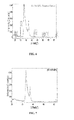
- FIG. 1 shows the nuclear magnetic resonance spectrum of Sb(NMeEt) 3 and FIG. 2 shows the nuclear magnetic resonance spectrum of Sb(NMe 2 ) 3 .
- FIG. 3 is a simultaneous thermal analysis (STA) graph for these two precursors, Sb(NMeEt) 3 and Sb(NMe 2 ) 3 , in which percentage thermogravimetry (TG) is plotted as a function of temperature, in degrees Centigrade.
- STA simultaneous thermal analysis
- antimony precursors can also be used. Such antimony precursors are suitable for use in forming GST films, in conjunction with the use of suitable germanium and tellurium precursors.
- antimony precursors include those of formulae (F), (G), (H), (I), (J), (K), (L) and (M), as defined below:
- Antimony precursors of a general type within the foregoing classes (F)-(M) include precursors having the following structures, wherein the various "R" groups in these structures are not necessarily numbered in exact correspondence with the substituent numberings in the above formulae, but nonetheless reflect the substituted positions in general fashion, which will be understood in reference to the above definitions of the substituents at the various positions of the associated molecules.
- the antimony precursors of classes (F)-(M) are usefully employed for deposition of antimony at low temperature with reducing co-reactants, e.g., reactants such as hydrogen, H 2 /plasma, amines, imines, hydrazines, silanes, silyl chalcogenides such as (Me 3 Si) 2 Te, germanes such as GeH 4 , ammonia, alkanes, alkenes, and alkynes.
- reactants such as hydrogen, H 2 /plasma, amines, imines, hydrazines, silanes, silyl chalcogenides such as (Me 3 Si) 2 Te, germanes such as GeH 4 , ammonia, alkanes, alkenes, and alkynes.
- the antimony precursors may be delivered for such deposition via liquid delivery techniques, in which precursors that are liquids may be used in neat liquid form, and precursors that are solids or liquids may be delivered in solutions or suspensions, in combination with suitable solvents, such as alkane solvents (e.g., hexane, heptane, octane, and pentane), aryl solvents (e.g., benzene or toluene), amines (e.g., triethylamine, tert-butylamine), imines and hydrazines.
- suitable solvents such as alkane solvents (e.g., hexane, heptane, octane, and pentane), aryl solvents (e.g., benzene or toluene), amines (e.g., triethylamine, tert-butylamine), imines and hydrazines.
- solid delivery techniques may be employed, in which the solid precursor is volatilized, to form a precursor vapor that is delivered to the deposition chamber for forming an antimony or antimony-containing film on the substrate.
- the solid precursor may be packaged for such use in a storage and dispensing package of suitable character, such as the ProE-Vap solid delivery and vaporizer unit commercially available from ATMI, Inc. (Danbury, CT, USA).
- the foregoing precursors may be usefully employed for CVD and ALD of Sb, Sb/Ge, Sb/Te and GST films.
- suitable solvents include alkanes (e.g., hexane, heptane, octane and pentane), aryl solvents (e.g., benzene, toluene), amines (e.g., triethylamine, tert-butylamine), imines, hydrazines and ethers.
- alkanes e.g., hexane, heptane, octane and pentane
- aryl solvents e.g., benzene, toluene
- amines e.g., triethylamine, tert-butylamine
- imines hydrazines and ethers.
- antimony precursors of the invention can be "fine-tuned" by choice of appropriate substituents, within the broad formulae set out hereinabove, to provide desired characteristics of thermal stability, volatility and compatibility with other co-reagents or components in a multi-component precursor system.
- antimony precursors of the invention are readily synthesized, by synthetic routes including those described below.
- the antimony precursor of the general formula (A): can for example be synthesized according to the following reaction scheme (A): and the antimony precursor of the general formula (B): can be synthesized according to the following reaction scheme (B): or by the following reaction scheme (C):
- the antimony precursor of the general formula (C) can be formed by synthesis in a corresponding manner.
- the antimony precursor of the general formula (D), having the following structure: can for example be synthesized according to the following reaction schemes (D), when n is zero, or (E), when n is 2: wherein X is halo (fluorine, bromine, chlorine, iodine).
- RMgX and RLi can be used as alternative synthesis reagents.
- tellurium complexes include those with beta-diketiminate ligands, which overcome the problems that many tellurium precursors used in deposition applications are very oxygen-sensitive and light-sensitive, and have an unpleasant odor.
- beta-diketiminate ligands By base stabilization with beta-diketiminate ligands, a tellurium precursor is obtained of a highly stable character with improved handling and shelf life characteristics, reduced odor, and sufficient volatility for deposition applications.
- the tellurium diketiminate complexes described herein can be used for CVD/ALD to form Te or Te-containing films. These compounds can be used in combination with Ge-and/or Sb-compounds to produce Te-Ge-, Te-Sb- or Ge-Sb-Te films in varied compositions.
- a general procedure to synthesize diketiminate ligands has been described in the literature, but such procedure is disadvantageous, since very bulky aryl substituents on the coordinating nitrogen atoms are required.
- alkyl ligands as iso-propyl, n-butyl, tert-butyl or amine-substituted alkyl groups, as for example ethylene-dimethylamine, can be advantageously used to produce superior tellurium diketiminate precursors for CVD/ALD applications.
- Smaller substituents on the nitrogen donor atoms provide sufficient volatility to form good films at low temperature.
- the ligands L can be used as the lithium salt or in a free imine form to synthesize the desired Te complexes.
- the free imine form of the ligand L can be reacted with a tellurium organic compound such as TeMe 4 to produce the desired Te species LTeMe 3 by methane elimination.
- TeMe 4 a tellurium organic compound
- the diketiminate ligands provide very effective base stabilization of the reactive metal center tellurium.
- the invention therefore provides a new class of Te complexes that provide greater stability and shelf life, while retaining sufficient volatility to form superior Te films via CVD/ALD at low temperatures.
- Additional tellurium complexes which can be used have the formulae (I) and (II): wherein R 1 , R 2 and R 3 they be the same as or different from one another, and each is independently selected from C 1 -C 6 alkyl, C 6 -C 10 aryl, silyl and C 1 -C 12 alkylamine (which includes both monoalkylamine as well as dialkylamine); and wherein R 1 , R 2 and R 3 they be the same as or different from one another, and each is independently selected from C 1 -C 6 alkyl, C 6 -C 10 aryl, silyl and C 1 -C 12 alkylamine (which includes both monoalkylamine as well as dialkylamine).
- beta-diketiminate ligands may for example be synthesized by the following procedure:
- tellurium complexes then can be synthesized by the following reaction: or alternatively by the following synthesis reaction: or by the following synthesis reaction:
- tellurium complexes described herein can be employed as CVD/ALD precursors for deposition of tellurium-containing thin films, e.g., by liquid injection of neat precursor material, or in organic solvent or by direct evaporation.
- the precursors described herein can be used to form amorphous germanium-containing films, as well as crystalline germanium-containing films, depending on the process conditions, deposition chamber configuration, substrate composition, etc.
- the determination of these process variables can readily be made by those of ordinary skill in the art, without undue experimentation, based on the disclosure herein and appropriate empirical effort involving varying process conditions and characterizing the resulting films, to establish a process condition envelope appropriate to a specific film-forming application.
- the germanium compounds described herein may be used with appropriate co-reactants in a continuous deposition mode (CVD) or pulsed/atomic layer deposition mode (ALD) to deposit films of superior character.
- CVD continuous deposition mode
- ALD pulsed/atomic layer deposition mode
- preferred co-reactants include O 2 and N 2 O for CVD, and more aggressive oxidizers for pulsed deposition, e.g., H 2 O, ozone, and O 2 plasma.
- reducing atmospheres are advantageously used.
- reducing agents such as H 2 , and NH 3 are preferred, and plasmas of these co-reactants may be used in digital or ALD mode, wherein the co-reactants are separated from the precursor in a pulse train, utilizing general CVD and ALD techniques within the skill of the art, based on the disclosure herein. More aggressive reducing agents can also be used in a digital or ALD mode since co-reactants can be separated, preventing gas phase reactions.
- the precursor preferably exhibits self-limiting behavior in one type of atmosphere (e.g., inert or weakly reducing/oxidizing gas environments) and exhibits rapid decomposition to form a desired film in another type of atmosphere (e.g., plasma, strongly reducing/oxidizing environments).
- one type of atmosphere e.g., inert or weakly reducing/oxidizing gas environments
- exhibits rapid decomposition to form a desired film in another type of atmosphere e.g., plasma, strongly reducing/oxidizing environments.
- Analogous metal cation precursors can be advantageously employed for CVD; while dissimilar species (i.e., different ligand species) can be employed in pulsed deposition.
- the precursors described herein can be utilized as low temperature deposition precursors with reducing co-reactants such as hydrogen, H 2 /plasma, amines, imines, hydrazines, silanes, silyl chalcogenides such as (Me 3 Si) 2 Te, germanes such as GeH 4 , ammonia, alkanes, alkenes and alkynes.
- reducing co-reactants such as hydrogen, H 2 /plasma, amines, imines, hydrazines, silanes, silyl chalcogenides such as (Me 3 Si) 2 Te, germanes such as GeH 4 , ammonia, alkanes, alkenes and alkynes.
- Liquid delivery formulations can be employed in which precursors that are liquids may be used in neat liquid form, or liquid or solid precursors may be employed in suitable solvents, including for example alkane solvents (e.g., hexane, heptane, octane, and pentane), aryl solvents (e.g., benzene or toluene), amines (e.g., triethylamine, tert-butylamine), imines and hydrazines.
- alkane solvents e.g., hexane, heptane, octane, and pentane
- aryl solvents e.g., benzene or toluene
- amines e.g., triethylamine, tert-butylamine
- imines and hydrazines e.g., triethylamine, tert-butylamine
- the thicknesses of metal-containing layers in the practice of the present invention can be of any suitable value.
- the thickness of the metal-containing layer can be in a range of from 5 nm to 500 nm or more.
- FIG. 1 is a schematic representation of a material storage and dispensing package 100 containing a germanium precursor, according to one embodiment of the present invention.
- the material storage and dispensing package 100 includes a vessel 102 that may for example be of generally cylindrical shape as illustrated, defining an interior volume 104 therein.
- the precursor is a solid at ambient temperature conditions, and such precursor may be supported on surfaces of the trays 106 disposed in the interior volume 104 of the vessel, with the trays having flow passage conduits 108 associated therewith, for flow of vapor upwardly in the vessel to the valve head assembly, for dispensing in use of the vessel.
- the solid precursor can be coated on interior surfaces in the interior volume of the vessel, e.g., on the surfaces of the trays 106 and conduits 108. Such coating may be affected by introduction of the precursor into the vessel in a vapor form from which the solid precursor is condensed in a film on the surfaces in the vessel.
- the precursor solid may be dissolved or suspended in a solvent medium and deposited on surfaces in the interior volume of the vessel by solvent evaporation.
- the precursor may be melted and poured onto the surfaces in the interior volume of the vessel.
- the vessel may contain substrate articles or elements that provide additional surface area in the vessel for support of the precursor film thereon.
- the solid precursor may be provided in granular or finely divided form, which is poured into the vessel to be retained on the top supporting surfaces of the respective trays 106 therein.
- the vessel 102 has a neck portion 109 to which is joined the valve head assembly 110.
- the valve head assembly is equipped with a hand wheel 112 in the embodiment shown.
- the valve head assembly 110 includes a dispensing port 114, which may be configured for coupling to a fitting or connection element to join flow circuitry to the vessel.
- flow circuitry is schematically represented by arrow A in Figure 1 , and the flow circuitry may be coupled to a downstream ALD or chemical vapor deposition chamber (not shown in Figure 1 ).
- the vessel 102 is heated, such input of heat being schematically shown by the reference arrow Q, so that solid precursor in the vessel is at least partially volatilized to provide precursor vapor.
- the precursor vapor is discharged from the vessel through the valve passages in the valve head assembly 110 when the hand wheel 112 is translated to an open valve position, whereupon vapor deriving from the precursor is dispensed into the flow circuitry schematically indicated by arrow A.
- the precursor may be provided in a solvent medium, forming a solution or suspension.
- Such precursor-containing solvent composition then may be delivered by liquid delivery and flash vaporized to produce a precursor vapor.
- the precursor vapor is contacted with a substrate under deposition conditions, to deposit the metal on the substrate as a film thereon.
- the precursor is dissolved in an ionic liquid medium, from which precursor vapor is withdrawn from the ionic liquid solution under dispensing conditions.
- the precursor may be stored in an adsorbed state on a suitable solid-phase physical adsorbent storage medium in the interior volume of the vessel.
- the precursor vapor is dispensed from the vessel under dispensing conditions involving desorption of the adsorbed precursor from the solid-phase physical adsorbent storage medium.
- Supply vessels for precursor delivery may be of widely varying type, and may employ vessels such as those commercially available from ATMI, Inc. (Danbury, Connecticut) under the trademarks SDS, SAGE, VAC, VACSorb, and ProE-Vap, as may be appropriate in a given storage and dispensing application for a particular precursor of the invention.
- the precursors of the invention thus may be employed to form precursor vapor for contacting with a substrate to deposit a germanium-containing thin film thereon.
- the invention utilizes the precursors to conduct atomic layer deposition, yielding ALD films of superior conformality that are uniformly coated on the substrate with high step coverage and conformality even on high aspect ratio structures.
- the precursors and processes described herein enable a wide variety of microelectronic devices, e.g., semiconductor products, flat panel displays, etc., to be fabricated with germanium-containing films of superior quality.
- the precursor compounds and processes described herein can be used to form GST films in combination with any suitable germanium and antimony precursors, e.g., by CVD and ALD techniques, for applications such as PCRAM device manufacture.
- the process conditions useful for carrying out deposition of Sb-containing films can be readily determined within the skill of the art by the simple expedient of selectively varying the delivery and deposition process conditions and characterizing the resulting films, to determine the process conditions envelope most appropriate for a given deposition application.
- antimony-containing films are formed on substrates, and can be, for example, GST films, amorphous SbTe films, or crystalline SbTe films, and can be applied, for example, using atomic layer deposition (ALD) or chemical vapor deposition (CVD) techniques.
- ALD atomic layer deposition
- CVD chemical vapor deposition
- SbTe e.g. Sb 2 Te 3
- thermoelectric devices may also be employed in thermoelectric devices.
- germanium butyl amidinate is employed, together with a tellurium precursor, e.g., a dialkyl tellurium precursor such as di-t-butyl tellurium, to yield amorphous GeTe by chemical vapor deposition or other suitable process.
- Amorphous films may be formed at any suitable process conditions. It will be recognized that the specific process conditions will be variable with respect to particular applications, and that varied types of deposition chambers may be employed in the formation of the amorphous GeTe film using the germanium butyl amidinate precursor of the invention.
- vapor deposition of germanium from the germanium alkyl amidinate may be conducted at temperature in a range of from about 200°C to about 400°C, and at pressure in a range of from about 0.1 to about 20 torr.
- the amorphous GeTe is formed using germanium butyl amidinate and t-butyl tellurium at a temperature of 320°C and 8 torr pressure, to form a GeTe film.
- Ge butyl amidinate and t-butyl tellurium precursors are utilized at a temperature of 350°C and 0.8 torr pressure, with an ammonia co-reactant, to form a GeTe film.
- GeTe deposition rate when the Te precursor is delivered by bubbler technique, depends strongly on the Te bubbler carrier flow, with higher carrier flows yielding thicker GeTe films of higher Te content. Nonetheless, incorporation of Te requires a relatively high deposition temperature and pressure, which tends to result in the formation of crystalline GeTe. By appropriately controlling temperature and pressure, stoichiometric amorphous GeTe films can be attained, which remain relatively smooth after crystallization.
- smooth amorphous GeTe films can be formed using other dialkyl Te precursors, such as diisopropyl Te.
- GeTe films are formed by CVD from such Ge precursor, with ammonia used as a co-reactant and Te(tBu) 2 employed as the Te precursor.
- GeBAMDN permits increased deposition temperatures and reduced deposition pressures to be used to overcome the problem of producing crystalline GeTe, when such Ge precursor is used with a suitable Te precursor for co-deposition of tellurium, e.g., a dialkyl Te precursor such as Te(tBu) 2 .
- Table 2 shows data for annealed GeTe films that were deposited at 8 Torr pressure after one hour annealing under nitrogen atmosphere at 400°C, as compared to the as-deposited film.
- Table 2 Film Thickness (A) AT% GE AT% TE AS-DEPOSITED 543.5 55.1 44.9 400°C, 1 HR ANNEAL UNDER N 2 501.6 55.8 44.2
- FIG. 2 is a scanning electron micrograph (SEM) of the annealed GeTe film, after annealing one hour under nitrogen atmosphere at 400°C
- FIG. 3 is a micrograph of the cross-section, in elevation, of the film, showing the SiO 2 substrate, TiN and GeTe layers.
- FIG. 3 shows that the film remained smooth after heat treatment.
- FIG. 4 is an x-ray dispersion plot for the annealed GeTe film of Table 2, of crystalline character after 400°C annealing.
- germanium butyl amidinate, GeBAMDN yielded smooth amorphous GeTe at temperature less than 320°C, e.g., with an ammonia co-reactant, at 8 torr pressure.
- deposition was carried out to determine the effects of temperature, pressure and tellurium delivery rate on GeTe deposition using nitrogen as a co-reactant.
- the experimental system included an oil bath maintained at a temperature of 100°C.
- a tellurium (tBu) 2 bubbler maintained at room temperature ( ⁇ 21.5°C) was employed and the Ge BAMDN precursor delivery rate was 20 micromoles/minute.
- Nitrogen co-reactant flow was 100 standard cubic centimeters per minute and pressure was fixed at 8,000 millitorr. Deposition times were 8 and 16 minutes. 50 nanometer thick TiN coated silicon substrates were used for the deposition. The data are set out in Table 3 below.
- FIGS. 6 and 7 are x-ray dispersion plots for films produced in these depositions.
- the film whose plot is shown in FIG. 6 utilized nitrogen as the co-reactant and
- FIG. 7 is the plot for deposition using an ammonia co-reactant.
- FIG. 8 is a scanning electron micrograph of crystalline GeTe, formed using hydrogen as a co-reactant.
- FIG. 9 is a scanning electron micrograph of the film produced using nitrogen as a co-reactant.
- FIG. 10 is a scanning electron micrograph of amorphous GeTe produced at a film thickness of 25 nanometers on the top surface of a 50 nanometer thick layer of titanium nitride.
- FIG. 11 shows an elevation section of the smooth amorphous GeTe film of FIG. 10 ..
- FIG. 12 is an energy dispersive spectrometry (EDS) spectrum of the GeTe film shown in FIGS. 10 and 11 , against a 50 nanometer thick GST film as a standard.
- EDS energy dispersive spectrometry
- Table 5 is a quantitative EDS analysis using the GST sample, Ge 2 Sb 2 Te 5 , as a standard.
- Table 5 Ge Sb Te Sample %Wt Atomic% %Wt Atomic% %Wt Atomic% GST_standard 13.99 22.00 23.45 22.00 62.57 56.00 GT_1132 17.71 61.64 0 0 19.38 38.37
- germanium (Ge), antimony (Sb), and tellurium (Te) were the only elements present, and that their respect weight percentages were 13.99, 23.45 and 62.57.
- silicon, carbon and oxygen were also present, but their peaks did not overlap with the elements of interest, and thus were considered non-interfering in the determination of germanium, antimony and tellurium in the GST sample.
- FIG. 13 is a scanning electron micrograph of GeTe on a microelectronic device structure, at an estimated thickness of about 300 Angstroms, and a composition of 68.4% germanium and 31.4% tellurium as determined analytically.
- Table 6 shows data on the effects of temperature on tellurium incorporation for GeTe deposition with ammonia co-reactant. The data included temperature, deposition rate, percent germanium, percent tellurium and crystallinity of the product film. Table 6 Run # Temperature (C) Dep rate (A/min) AT% Ge AT% Te Crystallinity 1137 340 61.2 44.7 54.9 crystalline 1136 320 29.2 60.3 39.5 amorphous 1143 300 26.4 75.6 24.4 amorphous 1138 280 24.5 83.3 26.6 amorphous 1139 260 23.0 87.20 12.6 amorphous
- FIG. 14 is a scanning electron micrograph of a GeTe film deposited at 340°C, showing the crystalline character thereof, which is also reflected in the XRD plot of FIG. 15 for such film.
- Table 7 shows data for annealing of amorphous germanium telluride films, as formed at 320°C and pressure of 8 torr, during a 16 minute deposition. Annealing was carried out in a tube furnace under a nitrogen atmosphere for a time of 10 minutes, at a temperature of 350°C which then was increased to 400°C. Annealing reduced the atomic percent of tellurium in the film and the film thickness.
- Table 7 Thickness (A) At% Ge At% Te Crystallinity As-deposited amorphous 350 °C, 10 min 400 °C, 10 min 436.3 53.1 46.4 Crystalline
- FIG. 16 is an x-ray dispersion plot of the 3 films for which data are shown in Table 7.
- the curve for the amorphous film is identified as that of sample GT-1134A.
- the sample subjected to 350°C annealing for 10 minutes was sample GT-1145A.
- FIG. 17 is a scanning electron micrograph of sample GT-1134, the amorphous GeTe film
- FIG. 18 is the scanning electron micrograph of the film annealed at 350°C followed by 400°C annealing, sample GT-1145B, showing tiny crystalline particles about 100 nanometers in size on top of the smooth film.
- Table 9 shows data reflecting the effects of tellurium delivery rate on germanium telluride deposition at 280°C in 3 respective runs conducted at 280°C, a pressure of 8 torr and with ammonium as a co-reactant.
- the tellurium carrier flow was 25 sccm in the first run, 40 sccm in the second run and 50 sccm in the third run, which produced deposition rates of 24.5, 28.5 and 24.2 Angstroms per minute, respectively.
- the data show that increasing the tellurium bubbler carrier flow from 40 to 50 sccm reduces the tellurium incorporation and the GeTe deposition rate.
- Table 9 Run # Te carrier flow (sccm) Deposition rate (A/min) AT% Ge AT% Te 1138 25 24.5 83.3 16.6 1140 40 28.5 72.9 26.9 1141 50 24.2 78.3 21.5
- the present invention enables the production of highly conformal GST films by the formation of smooth amorphous GeTe at suitable temperature and pressure process conditions.
- amorphous germanium telluride films are produced, which remain relatively smooth after crystallization.
- the germanium precursor can also be used with other dialkyl tellurium precursors, e.g., TeR 2 wherein R is C 3 -C 8 .
- Diisopropyl tellurium is a suitable alternative dialkyl tellurium precursor to di-tert-butyl tellurium as a Te source reagent.
- the germanium precursor can advantageously be [ ⁇ nBuC(iPrN) 2 ⁇ 2 Ge].
- the invention therefore contemplates the use of [ ⁇ nBuC(iPrN) 2 ⁇ 2 Ge] as a precursor for deposition of amorphous smooth germanium telluride films, with ammonia being useful as a co-reactant in the deposition process at higher temperatures and lower pressures.
- FIG. 19 is a scanning electron micrograph of a microelectronic device structure, as an example of an "aggressive" substrate on which GeTe has been deposited by chemical vapor deposition, using a germanium butyl amidinate precursor and a dialkyl tellurium precursor.
- the character of the GeTe material enables phase change random access memory (PCRAM) memory devices to be formed using amorphous germanium telluride films produced by use of the Ge BAMDN precursor of the invention.
- PCRAM phase change random access memory
- the GeTe film can be formed at temperature of 320°C, pressure of 7 torr, 5 micromoles/minute of GeBAMDN, 20 sccm carrier flow through a Te(tBu) 2 bubbler, and 50 sccm of ammonia.
- advantageous process conditions may involve temperature in a range of from about 280 to about 350°C, flow of 1-10 micromoles/minute of Ge, 1-100 sccm carrier flow, 1-1000 sccm NH 3 and pressure in a range of 1-20 torr.
- the invention in another aspect involves use of control agents to combat vapor phase pre-reaction of the precursors described herein, that otherwise causes uneven nucleation on the substrate, longer incubation times for deposition reactions, and lower quality product films.
- Such pre-reaction may for example be particularly problematic in applications involving chalcogenide films, related source materials (O, S, Se, Te, Ge, Sb, Bi, etc.), and/or manufacture of phase change memory and thermoelectric devices.
- Pre-reaction may occur when the precursor reagents described herein are introduced to the deposition chamber, as in chemical vapor deposition, and may also occur in atomic layer deposition (ALD) processes, depending on the specific arrangement of ALD cycle steps and the specific reagents involved.
- ALD atomic layer deposition
- the invention therefore contemplates the use of control agents with precursors described herein, whereby detrimental gas phase pre-reactions are suppressed, mitigated or eliminated, so that deposition reactions are induced/enhanced on the substrate surface, and films of superior character are efficiently formed.
- control agents that can be utilized with precursors described herein for such purpose include agents selected from the group consisting of (i) heteroatom (O, N, S) organo Lewis base compounds, (ii) free radical inhibitors, and (iii) deuterium-containing reagents.
- pre-reaction-combating agents described above can be introduced to any of the feed streams to the vapor deposition process in which the film is to be formed.
- pre-reaction-combating agents can be introduced to one or more of precursor feed stream(s), inert carrier gas stream(s) to which chalcogenide precursor(s) or other reagents are subsequently added for flow to the deposition chamber, co-reactant feed stream(s) flowed to the deposition chamber, and/or any other stream(s) that is/are flowed to the deposition chamber and in which the pre-reaction-combating agent(s) is/are useful for reduction or elimination of premature reaction of the precursors that would otherwise occur in the absence of such agent(s).
- the aforementioned suppressants, free radical inhibitors and/or deuterium source reagents in specific embodiments are co-injected with the precursor(s), e.g., metal source reagent(s), to effect at least partial reduction of pre-reaction involving the precursor(s) and reagent(s).
- precursor(s) e.g., metal source reagent(s)
- the pre-reaction-combatting agent can alternatively be added directed to the deposition locus, e.g., the deposition chamber to which the precursor vapor is introduced for contacting with the substrate to deposit the film thereon, to suppress deleterious vapor phase pre-reaction involving the precursor(s) and/or other reagents.
- the suppressant, free radical inhibitor and/or deuterium source can be added to a solution containing the precursor and/or another metal source reagent, and the resulting solution can be utilized for liquid delivery processing, in which the solution is flowed to a vaporizer to form a source vapor for contacting with the substrate to deposit the deposition species thereon.
- the suppressant, free radical inhibitor and/or deuterium source can be added to form a mixture or a solution with the precursor and/or another metal source reagent, depending on the respective phases of the materials involved, and their compatibility/solubility.
- the suppressant, free radical inhibitor and/or deuterium source can be utilized for surface treatment of the substrate prior to contacting of the substrate with the precursor and/or other metal source reagent.
- the invention therefore contemplates various vapor deposition compositions and processes for forming films on substrates, in which pre-reaction of the precursors is at least partially attenuated by one or more pre-reaction-combating agents selected from among heteroatom (O, N, S) organo Lewis base compounds, sometimes herein referred to as suppressor agents, free radical inhibitors, and/or deuterium source reagents.
- pre-reaction-combating agents selected from among heteroatom (O, N, S) organo Lewis base compounds, sometimes herein referred to as suppressor agents, free radical inhibitors, and/or deuterium source reagents.
- the control agent can be used for combating pre-reaction of chalcogenide precursor in a process in which multiple feed streams are flowed to a deposition locus to form a film on a substrate, wherein at least one of the multiple feed streams includes a precursor susceptible to pre-reaction adversely affecting the film, in which the method involves introducing the control agent to at least one of such multiple feed streams or supplied materials therefor, or to the deposition locus.
- the pre-reaction combating reagent alternatively can be introduced to passivate the surface of a growing chalcogenide film or slow the deposition rate, followed by reactivation using an alternative precursor or co-reactant (for example H 2 , NH 3 , plasma, H 2 O, hydrogen sulfide, hydrogen selenide, diorganotellurides, diorganosulfides, diorganoselenides, etc.), thereby carrying out passivation/retardation followed by reactivation steps, e.g., as an alternating repetitive sequence.
- Such sequence of passivation/retardation followed by reactivation can be carried out for as many repetitive cycles as desired, in ALD or ALD-like processes. The steps may be carried out for the entire deposition operation, or during some initial, intermediate or final portion thereof.
- the invention therefore contemplates precursor compositions including the precursor and the pre-reaction-combating reagent.
- pre-reaction-combating reagents within the categories of pre-reaction-combating reagents previously described, viz., (i) heteroatom (O, N, S) organo Lewis base compounds, (ii) free radical inhibitors, and (iii) deuterium-containing reagents, suitable pre-reaction-combating reagents for specific applications may be readily determined within the skill of the art, based on the disclosure herein.
- Heteroatom (O, N, S) organo Lewis base compounds may be of varied type, e.g., containing an oxo (-O-) moiety, a nitrogen ring atom or pendant amino or amide substituent, a sulfur ring atom or pendant sulfide, sulfonate or thio group, as effective to at least partially lessen pre-reaction of the precursor and other organo metal reagents in the process system.
- heteroatom (O, N, S) organo Lewis base compounds having utility in specific applications of the invention include, without limitation, 1,4-dioxane, thioxane, ethers, polyethers, triethylamine, triazine, diamines, N,N,N',N'-tetramethylethylenediamine, N,N,N'-trimethylethylenediamine, amines, imines, pyridine, and the like.
- heteroatom organo Lewis base compounds for such purpose includes R 3 N, R 2 NH, RNH 2 , R 2 N(CH 2 ) x NR 2 , R 2 NH(CH 2 ) x NR 2 , R 2 N(CR 2 ) x NR 2 , and cyclic amines -N(CH 2 ) x -, imidazole, thiophene, pyrrole, thiazole, urea, oxazine, pyran, furan, indole, triazole, triazine, thiazoline, oxazole, dithiane, trithiane, crown ethers, 1,4,7-triazacyclononane, 1,5,9-triazacyclododecane, cyclen, succinamide, and substituted derivatives of the foregoing, wherein R can be hydrogen or any suitable organo moieties, e.g., hydrogen, C 1 -C 8 alkyl, C 1 -
- the heteroatom organo Lewis base compounds may be utilized in the precursor composition at any suitable concentration, as may be empirically determined by successive deposition runs in which the heteroatom organo Lewis base compound concentration is varied, and character of the resulting film is assessed, to determine an appropriate concentration.
- the heteroatom organo Lewis base compound may be utilized in the concentration of 1-300% of the amount of precursor. Specific sub-ranges of concentration values within a range of 0.01-3 equivalents of the heteroatom organo Lewis base compound may be established for specific classes of precursors, without undue experimentation, based on the disclosure herein.
- the pre-reaction-combating reagent may additionally or alternatively comprise free radical inhibitors that are effective to lessen the extent of pre-reaction between the precursor and another organo metal reagent.
- free radical inhibitors may be of any suitable type, and may for example include hindered phenols.
- Illustrative free radical inhibitors include, without limitation, free radical scavengers selected from the group consisting of: 2,6-ditert-butyl-4-methyl phenol, 2,2,6,6-tetramethyl-1-piperidinyloxy, 2,6-dimethylphenol, 2-tert-butyl-4-hydroxyanisole, 3-tert-butyl-4-hydroxyanisole, propyl ester 3,4,5-trihydroxy-benzoic acid, 2-(1,1-dimethylethyl)-1,4 benzenediol, diphenylpicrylhydrazyl, 4-tert-butylcatechol, N-methylaniline, 2,6-dimethylaniline, p-methoxydiphenylamine, diphenylamine, N,N'-diphenyl-p-phenylenediamine, p-hydroxydiphenylamine, phenol, octadecyl-3-(3,5-di-tert-butyl-4 -hydroxyphenyl)
- Useful concentrations of the free radical inhibitor may be in a range of from 0.001 to about 0.10% by weight of the weight of the precursor, in various specific embodiments. More generally, any suitable amount of free radical inhibitor may be employed that is effective to combat the pre-reaction of the precursor in the delivery and deposition operations involved in the film formation process.
- deuterium source compounds afford another approach to suppressing pre-reaction of the chalcogenide precursor.
- Such deuterium source compounds may be of any suitable type, and may for example include deuterated pyridine, deuterated pyrimidine, deuterated indole, deuterated imidazole, deuterated amine and amide compounds, deuterated alkyl reagents, etc., as well as deuterated analogs of the precursors that would otherwise be used as containing hydrogen or protonic substituents.
- Deuterides that may be useful in the general practice of invention as pre-reaction-combating reagents include, without limitation, germanium and antimony compounds of the formulae R x GeD 4-x and R x SbD 3-x wherein R can be hydrogen or any suitable organo moieties, e.g., hydrogen, C 1 -C 8 alkyl, C 1 -C 8 alkoxy, C 1 -C 8 alkene, C 1 -C 8 alkyne, and C 1 -C 8 carboxyl, and wherein x is an integer having a value of from 1 to 6.
- the deuterium source reagent may be utilized at any suitable concentration that is effective to combat pre-reaction of the precursor.
- Illustrative deuterium source reagent concentrations in specific embodiments of the invention can be in a range of 0.01 to about 5% by weight, based on the weight of precursor.
- a deuterium source compound may be added to one or more of the feed streams to the vapor deposition process, and/or one of the precursors or other feed stream components may be deuterated in the first instance.
- concentrations of the pre-reaction-combating agents utilized in the practice of the present invention to at least partially eliminate pre-reaction of the precursors can be widely varied in the general practice of the present invention, depending on the temperatures, pressures, flow rates and specific compositions involved.
- concentration of the pre-reaction-combating reagents of the invention therefore are to be appreciated as being of an illustrative character only, with applicable concentrations being readily determinable within the skill of the art, based on the disclosure herein.
- the specific mode of introduction or addition of the pre-reaction-combating agent to one or more of the feed streams to the deposition process may correspondingly be varied, and may for example employ mass flow controllers, flow control valves, metering injectors, or other flow control or modulating components in the flow circuitry joining the source of the pre-reaction-combating agent with the streams being flowed to the deposition process during normal film-forming operation.
- the process system may additionally include analyzers, monitors, controllers, instrumentation, etc., as may be necessary or appropriate to a given implementation of the invention.
- the pre-reaction-combating agent may be mixed with precursor in the first instance, as a starting reagent material for the process.
- the pre-reaction-combating agent may be mixed in liquid solution with the precursor, for liquid delivery of the resulting precursor solution to a vaporizer employed to generate precursor vapor for contact with the substrate to deposit the film thereon.
- the pre-reaction-combating agent may be added to the deposition locus to provide active gas-phase suppression of pre-reaction of the precursor vapor(s) that would otherwise be susceptible to such deleterious interaction.
- the pre-reaction-combating agent may be used as a preliminary surface treatment following which the precursor and co-reactants (e.g., H 2 , NH 3 , plasma, H 2 O, hydrogen sulfide, hydrogen selenide, diorganotellurides, diorganosulfides, diorganoselenides, etc.) are delivered to the substrate surface to effect deposition on such surface.
- the pre-reaction-combating agent may be introduced into one of more of the flow lines to the deposition process and flow to the substrate in the deposition process chamber, prior to initiation of flow of any precursors. After the requisite period of contacting of the substrate with such pre-reaction-combating agent has been completed, the flow of the pre-reaction-combating agent can be terminated, and normal feeding of flow streams to the deposition chamber can be initiated.
- the pre-reaction-combating agent may be introduced in any of a wide variety of ways to effect diminution of the pre-reaction of the precursor in the deposition system.
- a vapor phase deposition system comprising:
- FIG. 20 is a schematic representation of a vapor deposition system 100 in one embodiment thereof
- a pre-reaction-combating agent is contained in a supply vessel 110.
- the pre-reaction-combating agent can comprise a pre-reaction suppressant, a free radical inhibitor, a deuterium source, or a combination of two or more of such agents and/or types of such agents.
- the pre-reaction-combating agent supply vessel is joined by respective flow lines 112, 114 and 116, to germanium, antimony and tellurium reagent supply vessels, labeled “G,” “S” and “T,” respectively.
- the germanium precursor in vessel “G” may be a tetraalkyl or tetraamido germanium compound, such as tetramethyl germanium, tetraethyl germanium, tetraallyl germanium, tetrakis(dimethylamino)germane or other organo germanium compounds.
- precursor “G” may be a germylene compound wherein the lone pair on Ge(II) can react in the gas-phase with chalcogen precursors in the absence of a pre-reaction suppresant.
- the antimony precursor in vessel “S” can be a trialkyl or triamido antimony compound, such as tributyl antimony, triisopropyl antimony, tris(dimethylamino)antimony or other organo antimony compound.
- the tellurium precursor in vessel “T” can be a dialkyl or diamido tellurium compound, such as diisopropyl tellurium, dibutyl tellurium, bis[bis(trimethylsilyl)amino]tellurium or other organo tellurium compound.
- the pre-reaction-combating agent therefore can be added to any of the germanium, antimony and/or tellurium precursors in the respective "G,” “S” and “T” vessels, via the corresponding flow line(s), which for such purpose may have flow control valves or other flow-modulating components therein.
- the germanium, antimony and tellurium precursors are flowed in liquid form in feed lines 118, 120 and 122, respectively, to the mixing chamber 124, and the resulting precursor mixture then is flowed from the mixing chamber 124 in line 126 to vaporizer 128.
- the liquid precursor mixture and pre-reaction-combating agent are volatilized to form a precursor vapor.
- the precursor vapor then flows in line 130 to the showerhead disperser 134 in vapor deposition chamber 132, for discharge of precursor mixture onto the wafer substrate 136 mounted on susceptor 138 in the deposition chamber.
- the precursor vapor contacting the wafer substrate 136 serves to deposit the germanium, antimony and tellurium metals on the substrate, to form a thin film of germanium-antimony-tellurium (GST) material, e.g., for manufacture of a phase change random access memory device.
- GST germanium-antimony-tellurium
- the contacted precursor vapor, depleted in metals content, is discharged from the vapor deposition chamber 132 in line 140, and flows to the effluent abatement unit 142.
- the discharged effluent vapor is treated, e.g., by scrubbing, catalytic oxidation, electrochemical treatment, or in other manner, to yield a final effluent that is discharged from the abatement unit in line 146.
- the schematic representation of the vapor deposition system shown in FIG. 20 is of an illustrative character, and that numerous other arrangements could be utilized for deployment and use of the pre-reaction-combating agent, including those previously illustratively discussed herein.
- the pre-reaction-combating agent could be introduced directly to the mixing chamber 124, for blending therein with the respective GST precursors.
- the pre-reaction-combating agent could be introduced into manifold 118, or other mixing chamber, blender, etc., for combination with the precursor that is being transported to the deposition locus.
- the system shown in FIG. 20 employs liquid delivery of the respective precursors. It will be recognized that if solid-phased precursors are employed, then solid delivery techniques may be employed, in which solid precursor is volatilized, e.g., by sublimation of the solid starting material.
- one or more of the germanium, antimony and tellurium precursors could be supplied in the first instance as a deuterated analog of an organo germanium, antimony or tellurium precursor, in which hydrogen substituents of the organo moiety have been replaced with deuterium.
- the pre-reaction-combating reagents may be employed in the broad practice of the present invention to produce improved films for the manufacture of semiconductor products.
- the pre-reaction-combating reagents described herein may be utilized in various combinations in specific applications, to suppress or eliminate pre-reaction of the precursor and provide superior nucleation and final film properties.
Landscapes
- Chemical & Material Sciences (AREA)
- Engineering & Computer Science (AREA)
- Organic Chemistry (AREA)
- Metallurgy (AREA)
- General Chemical & Material Sciences (AREA)
- Chemical Kinetics & Catalysis (AREA)
- Materials Engineering (AREA)
- Mechanical Engineering (AREA)
- Plasma & Fusion (AREA)
- Physics & Mathematics (AREA)
- Electromagnetism (AREA)
- Inorganic Chemistry (AREA)
- Manufacturing & Machinery (AREA)
- Chemical Vapour Deposition (AREA)
- Semiconductor Memories (AREA)
Abstract
Description
- The benefit of priority of
U.S. Provisional Patent Application 61/051,274 filed May 7, 2008 U.S. Provisional Patent Application 61/052,018 filed May 9, 2008 U.S. Provisional Patent Application 61/076,428 filed June 27, 2008 U.S. Provisional Patent Application 60/984,370 filed October 31, 2007U.S. Provisional Patent Application 61/050,179 filed May 2, 2008 U.S. Provisional Patent Application 61/051,274 U.S. Provisional Patent Application 61/052,018 U.S. Provisional Patent Application 61/076,428 U.S. andProvisional Patent Application 60/984,370U.S. Provisional Patent Application 61/050,179 - The present invention relates to a chemical vapor deposition process for forming amorphous films including germanium, tellurium and/or antimony on substrates, including, for example, germanium telluride (GeTe) and germanium antimony telluride (GST) films, as well as phase change random access memory devices and other devices incorporating such films. In particular, the present invention relates to amorphous GeTe and GST films formed from CVD processes, and devices formed from these films.
- Phase change random access memory (PCRAM) has attracted a great deal of interest recently for highly integrated non-volatile memory devices. In PCRAM cells, the high level of reset current that is required for switching the GST material from the crystalline to the amorphous state has been the major obstacle to the further scaling of PCRAM. Confining an alloy of germanium, antimony, and tellurium (GST) material into the contact plug, which greatly reduces the heat dissipation to the surrounding material, profoundly reduces the reset current. Therefore, it is necessary to deposit the GST film using a process that offers good conformality, such as atomic layer deposition (ALD) or chemical vapor deposition (CVD) processes. The ALD process is very time consuming, as it builds up the film "layer by layer". On the contrary, the CVD process offers a high deposition rate. Unfortunately, the CVD process tends to yield crystalline GeTe. The crystalline GeTe significantly reduces the conformality of the GST film, and often creates voids in the contact plug.
- It would be advantageous to provide new processes for forming GST, GeTe, and other films in an amorphous manner, but with a relatively high deposition rate. The present invention provides such processes.
- Improved chemical vapor deposition processes for forming amorphous GeTe and GST films on substrates, for applications such as PCRAM highly integrated non-volatile memory devices, are disclosed. The germanium and tellurium precursors described herein can be reacted in a reducing environment with ammonia, or, in some embodiments, in a nitrogen atmosphere, at a controlled temperature and pressure, to yield amorphous GeTe.
- In one embodiment, the temperature of the deposition is 320°C or less, and the pressure is 8 torr or less. In another embodiment, the temperature is 350°C or less, and the pressure is 0.8 torr or less. Deposition of Ge from the germanium precursors (such as GeM or Ge amidinate) is fast at low temperatures. However, Te incorporation requires a relatively high deposition temperature and pressure, which tends to result in the formation of crystalline GeTe. By controlling both the temperature and pressure, an amorphous GeTe film can be attained. This amorphous GeTe film remains relatively smooth after crystallization. This process can also be extended to other dialkyl Te precursors, such as di-isopropyl Te.
- In another aspect, the present invention relates to a process for depositing an amorphous GeTe material on a substrate by chemical vapor deposition from a precursor which is vaporized to form a precursor vapor which is then contacted with the substrate. Representative precursors for depositing the amorphous GeTe films include Ge butylamidinate, (GeBAMDN) and [{nBuC(iPrN)2Ge], also referred to herein as GeM.
- In one specific aspect of the invention, Ge butyl amidinate or GeM ({nBuC(iPrN)2}2Ge) have been developed, together with t-butyl Te, to yield amorphous GeTe at 320°C and 8 torr pressure, and 350°C at 0.8 torr pressure with ammonia co-reactant.
- In another aspect of the invention, a process for crystallizing an amorphous GeTe film to yield a relatively smooth GeTe film is described. While deposition of Ge from Ge amidinate or GeM is fast at low temperatures, incorporation of Te requires a relatively high deposition temperature and pressure, which tends to result in the formation of crystalline GeTe. Crystalline GeTe yields a thin film that is not smooth. By controlling both the temperature and pressure, an amorphous GeTe film can be attained. The amorphous GeTe film remains relatively smooth after crystallization.
- In another aspect of the invention, this process can also be extended to other dialkyl Te precursors, such as di-isopropyl Te.
- In a further aspect, the invention relates to a method of forming a GeTe, GST, antimony, or other such film on a substrate, said method comprising volatilizing a germanium, antimony, or tellurium precursor described herein to form a precursor vapor, and contacting such precursor vapor with a substrate to form the germanium-, antimony-, and/or tellurium-containing film thereon.
- In another aspect, the invention relates to a precursor composition for forming a germanium-containing film, comprising [{nBuC(iPrN)2}2Ge], also referred to herein as GeM.
- Another aspect of the invention relates to a smooth amorphous germanium telluride or germanium-antimony-telluride film.
- A further aspect of the invention relates to a method of forming a smooth amorphous germanium telluride film, comprising volatilizing [{nBuC(iPrN)2}2Ge] and a diakyl tellurium precursor to form a precursor vapor and contacting the precursor vapor with a substrate to form the smooth amorphous germanium telluride film on the substrate.
- In another aspect, the invention relates to a method of forming a phase change random access memory device, comprising forming a germanium telluride film of amorphous character, comprising chemical vapor deposition of germanium from a germanium precursor comprising [{nBuC(iPrN)2}2Ge] or Ge butylamidinate.
- The invention in another aspect relates to a method of making a PCRAM device, comprising forming a GeTe or GST film on a substrate for fabrication of said device, wherein said forming comprises depositing a film layer on the substrate from the vapor of a precursor described herein, using the processes for depositing amorphous germanium, tellurium, and or antimony layers described herein.
- The precursors can be used to form a GST film on a substrate, by depositing one or more of the antimony-containing precursors described herein along with one or more germanium and tellurium-containing precursors on the substrate from a vapor comprising the precursors.
- The precursors can also be used to form PCRAM devices, by forming a GST film on a substrate for fabrication of said device as described above.
- In yet another aspect, the invention relates to a method of combating pre-reaction of the precursors described herein in a vapor deposition process for forming a film on a substrate, wherein the precursor is susceptible to pre-reaction adversely affecting the film, said method comprising introducing to said process a pre-reaction-combating agent selected from the group consisting of (i) heteroatom (O, N, S) organo Lewis base compounds, (ii) free radical inhibitors, and (iii) deuterium-containing reagents.
- Another aspect of the invention relates to a method of combating pre-reaction of the precursors described herein in a vapor deposition process in which multiple feed streams are flowed to a deposition locus to form a film on a substrate, wherein at least one of said multiple feed streams includes a precursor susceptible to pre-reaction adversely affecting the film, said method comprising introducing to at least one of said multiple feed streams or supplied materials therefor, or to the deposition locus, a pre-reaction-combating agent selected from the group consisting of (i) heteroatom (O, N, S) organo Lewis base compounds, (ii) free radical inhibitors, and (iii) deuterium-containing reagents.
- A still further aspect of the invention relates to a composition, comprising a precursor and a pre-reaction-combating agent for said precursor, said pre-reaction-combating agent being selected from the group consisting of (i) heteroatom (O, N, S) organo Lewis base compounds, (ii) free radical inhibitors, and (iii) deuterium-containing reagents.
- In a further aspect, the invention relates to a method of combating pre-reaction of a vapor phase precursor as described herein in contact with a substrate for deposition of a film component thereon, comprising contacting said substrate, prior to said contact of the vapor phase precursor therewith, with a pre-reaction-combating agent selected from the group consisting of (i) heteroatom (O, N, S) organo Lewis base compounds, (ii) free radical inhibitors, and (iii) deuterium-containing reagents.
- In a further aspect, the invention relates to a process wherein the pre-reaction combating reagent is introduced to passivate the surface of a growing film or slow the deposition rate, followed by reactivation using an alternative precursor or co-reactant (for example H2, NH3, plasma, H2O hydrogen sulfide, hydrogen selenide, diorganotellurides, diorganosulfides, diorganoselenides, etc.). Such passivation/retardation followed by reactivation thus may be carried out in an alternating repetitive sequence, for as many repetitive cycles as desired, in ALD or ALD-like processes. Prereaction-combating agents can be selected from the group consisting of (i) heteroatom (O, N, S) organo Lewis base compounds, (ii) free radical inhibitors, and (iii) deuterium-containing reagents.
- Another aspect of the invention relates to a vapor phase deposition process for forming a film on a substrate involving cyclic contacting of the substrate with at least one film precursor described herein that is undesirably pre-reactive in the vapor phase, such process comprising introducing to said film during growth thereof a pre-reaction-combating reagent that is effective to passivate a surface of said film or to slow rate of deposition of said film precursor, and after introducing said pre-reaction-combating reagent, reactivating said film with a different film precursor.
- The invention relates in a further aspect to a method of forming a germanium-containing film on a substrate by a vapor deposition process, comprising volatilizing a germanium precursor to form a germanium precursor vapor, optionally combining the precursor vapor with a component selected from the group consisting of ammonia, hydrogen, helium, argon, and nitrogen, and contacting the precursor vapor with a substrate for vapor deposition of the germanium-containing film thereon, wherein the germanium precursor is selected from the group consisting of the following germanium compositions:

- R1 and R2 may be the same as or different from one another, and are independently selected from H, C1-C6 alkyl, C2-C5 alkenyl, C5-C10 cycloalkyl, C6-C10 aryl, and -Si(R3)3 wherein each R3 is independently selected from C1-C6 alkyl;

- R and R' may be the same as or different from one another, and each R and R' is independently selected from H, C1-C6 alkyl, C2-C5 alkenyl, C5-C10 cycloalkyl, C6-C10 aryl, and -Si(R3)3 wherein each R3 is independently selected from C1-C6 alkyl;

- R, R', R1 and R2 may be the same as or different from one another, and each is independently selected from H, C1-C6 alkyl, C2-C5 alkenyl, C5-C10 cycloalkyl, C6-C10 aryl, and -Si(R3)3 wherein each R3 is independently selected from C1-C6 alkyl;
(R)4-nGe(NR1R2)n IV
- R, R1 and R2 may be the same as or different from one another, and each is independently selected from H, C1-C6 alkyl, C2-C5 alkenyl, C5-C10 cycloalkyl, C6-C10 aryl, and -Si(R3)3 wherein each R3 is independently selected from C1-C6 alkyl; and n is an integer from 0 to 4 inclusive;

- R1, R2, R3, R4, R5 and R6 may be the same as or different from one another, and each is independently selected from H, C1-C6 alkyl, C2-C5 alkenyl, C5-C10 cycloalkyl, C6-C10 aryl, and -Si(R3)3 wherein each R3 is independently selected from C1-C6 alkyl;

- R is selected from H, C1-C6 alkyl, and C6-C10 aryl; and
- x is 0, 1 or 2;

- R1, R2, R3 and R4 may be the same as or different from the others, and each is independently selected from among H, C1-C6 alkyl, C5-C10 cycloalkyl, C6-C10 aryl, and - Si(R3)3 wherein each R3 is independently selected from C1-C6 alkyl;

- R1, R2, R3, R4, and R5 may be the same as or different from one another, and each is independently selected from among H, C1-C6 alkyl, silyl, -Si(R')3, C6-C10 cycloalkyl, C6-C10 aryl, -(CH2)xNR'R", and -(CH2)xOR"', wherein x = 1, 2 or 3, and R', R" and R"' may be the same as or different from one another, and each is independently selected from C1-C6 alkyl;

- R' and R" may be the same as or different from one another, and are independently selected from among H, C1-C6 alkyl, C5-C10 cycloalkyl, C6-C10 aryl, and -Si(R3)3 wherein each R3 is independently selected from C1-C6 alkyl; and
- each X is independently selected from among C1-C6 alkyl, C1-C6 alkoxy, -NR1R2, and -C(R3)3, wherein each of R1, R2 and R3 is independently selected from H, C1-C6 alkyl, C5-C10 cycloalkyl, C6-C10 aryl, and -Si(R4)3 wherein each R4 is independently selected from C1-C6 alkyl;

- R1, R2, R3 and R4 may be same as or different from one another, and are independently selected from among H, C1-C6 alkyl, C5-C10 cycloalkyl, C6-C10 aryl, and - Si(R3)3 wherein each R3 is independently selected from C1-C6 alkyl;

- R1, R2, R3 and R4 may be the same as or different from one another, and are independently selected from among H, C1-C6 alkyl, C5-C10 cycloalkyl, C6-C10 aryl, and - Si(R3)3 wherein each R3 is independently selected from C1-C6 alkyl;

- R1, R2, R3 and R4 may be the same as or different from one another, and are independently selected from among H, C1-C6 alkyl, C5-C10 cycloalkyl, C6-C10 aryl, and - Si(R3)3 wherein each R3 is independently selected from C1-C6 alkyl;
R1R2R3R4Ge XVI
- R1, R2, R3, and R4 may be the same as or different from one another, and are independently selected from among H, C1-C6 alkyl, C5-C10 cycloalkyl, C6-C10 aryl, and - Si(R3)3 wherein each R3 is independently selected from C1-C6 alkyl,


- Ge(NMe2)4, Ge(NEtMe)4, Ge(NEt2)4, iPr3GeCl, iPr3GeNMe2, iPr3GeNEtMe, iPr3GeNEt2, Ge butylamidinate, and [{nBuC(iPrN)2}2Ge].
- Another aspect of the invention relates to a germanium precursor, selected from the group consisting of the above-specified germanium precursor species.
- A still further aspect of the invention relates to a smooth amorphous germanium telluride or germanium antimony telluride film, as formed by the method described above, using a germanium precursor comprising Ge butylamidinate or [{nBuC(iPrN)2}2Ge].
- Other aspects, features and embodiments of the invention will be more fully apparent from the ensuing disclosure and appended claims.
-
-
FIG. 1 is a schematic representation of a material storage and dispensing package containing a precursor of the present invention, in one embodiment thereof. -
FIG. 2 is a scanning electron micrograph of a germanium telluride film after annealing at one hour in nitrogen atmosphere, at 400°C. -
FIG. 3 is a cross-sectional elevation SEM view of the germanium telluride film ofFIG. 2 , showing the smooth character of the germanium telluride film deposited on the titanium nitride layer formed on the silicon dioxide substrate. -
FIG. 4 is an x-ray dispersion (XRD) plot of a germanium telluride film, showing its crystalline character after annealing at 400°F. -
FIG. 5 is an XRD plot of a germanium telluride film deposited in a CVD process with a nitrogen co-reactant. -
FIG. 6 is an XRD plot of a germanium telluride film deposited in a CVD process using a nitrogen co-reactant. -
FIG. 7 an XRD plot of a germanium telluride film deposited in a CVD process using an ammonia co-reactant. -
FIG. 8 is a scanning electron micrograph of a crystalline germanium telluride film formed deposited in a CVD process using hydrogen as a co-reactant. -
FIG. 9 is a scanning electron micrograph of a crystalline germanium telluride film formed in a CVD process using nitrogen as a co-reactant. -
FIG. 10 is a scanning electron micrograph of an amorphous germanium telluride film formed on a 50 nanometer thickness of titanium nitride. -
FIG. 11 is a cross-sectional elevation view of the germanium telluride film ofFIG. 10 . -
FIG. 12 is an EDS spectra plot of germanium telluride and a standard GST film. -
FIG. 13 is a scanning electron micrograph of a film of germanium telluride deposited on a microelectronic device structure. -
FIG. 14 is a scanning electron micrograph of a crystalline germanium telluride film, deposited at 340°C. -
FIG. 15 is an XRD plot for the germanium telluride film ofFIG. 14 . -
FIG. 16 is an XRD plot for various germanium telluride films, including an amorphous film, a film annealed at 350°C for 10 minutes, and a germanium telluride film annealed at 350°C followed by 400°C exposure, for 10 minutes. -
FIG. 17 is a scanning electron micrograph of an amorphous germanium telluride film. -
FIG. 18 is a scanning electron micrograph of a germanium telluride film, after 400°C annealing. -
FIG. 19 is a scanning electron micrograph of a microelectronic device structure, as an example of an "aggressive" substrate on which GeTe has been deposited by chemical vapor deposition, using a germanium butyl amidinate precursor and a dialkyl tellurium precursor. -
FIG. 20 is a schematic representation of a vapor deposition system according to one embodiment of the present invention, wherein suppression of pre-reaction of the precursors is achieved by addition of pre-reaction-combating reagent to one or more feed streams in the vapor deposition system. - The present invention relates to the use of various germanium, tellurium, and antimony precursors, having utility for forming highly conformal germanium-containing films by low temperature (< 300°C) vapor deposition processes such as CVD and ALD, in methods for forming germanium-containing films. In other aspects, the invention relates to films formed using the methods, and microelectronic device products incorporating such films.
- The precursors described herein are usefully employed in chemical vapor deposition and atomic layer deposition processes to form germanium-containing films, such as films of GeTe, GST, and the like. The GeTe films can be GexTel-x systems, as such are defined in Scharnhorst and Riedl, "Photoconductivity in the amorphous Ge-rich GexTe1-x system," Journal of Applied Physics, Vol. 45, p.2971-2979 (1974), or GexSbyTez films, as such are described, for example, in Tsu, Journal of Vacuum Science & Technology A: Vacuum, Surfaces, and Films, Volume 17, Issue 4, July 1999, pp.1854-1860 (1999), the contents of both of which are hereby incorporated by reference. The films can advantageously be formed, using the processes described herein, to result in a substantially amorphous film layer.
- The invention will be better understood with reference to the following definitions:
- As used herein, the term "film" refers to a layer of deposited material having a thickness below 1000 micrometers, e.g., from such value down to atomic monolayer thickness values. In various embodiments, film thicknesses of deposited material layers in the practice of the invention may for example be below 100, 10, or 1 micrometers, or in various thin film regimes below 200, 100, or 50 nanometers, depending on the specific application involved. As used herein, the term "thin film" means a layer of a material having a thickness below 1 micrometer.
- As used herein, the singular forms "a", "and", and "the" include plural referents unless the context clearly dictates otherwise.
- As used herein, the identification of a carbon number range, e.g., in C1-C12 alkyl, is intended to include each of the component carbon number moieties within such range, so that each intervening carbon number and any other stated or intervening carbon number value in that stated range, is encompassed, it being further understood that sub-ranges of carbon number within specified carbon number ranges may independently be included in smaller carbon number ranges, within the scope of the invention, and that ranges of carbon numbers specifically excluding a carbon number or numbers are included in the invention, and sub-ranges excluding either or both of carbon number limits of specified ranges are also included in the invention. Accordingly, C1-C12 alkyl is intended to include methyl, ethyl, propyl, butyl, pentyl, hexyl, heptyl, octyl, nonyl, decyl, undecyl and dodecyl, including straight chain as well as branched groups of such types. It therefore is to be appreciated that identification of a carbon number range, e.g., C1-C12, as broadly applicable to a substituent moiety, enables, in specific embodiments of the invention, the carbon number range to be further restricted, as a sub-group of moieties having a carbon number range within the broader specification of the substituent moiety. By way of example, the carbon number range e.g., C1-C12 alkyl, may be more restrictively specified, in particular embodiments of the invention, to encompass sub-ranges such as C1-C4 alkyl, C2-C8 alkyl, C2-C4 alkyl, C3-C5 alkyl, or any other sub-range within the broad carbon number range.
- The precursors of the invention may be further specified in specific embodiments by provisos or limitations excluding specific substituents, groups, moieties or structures, in relation to various specifications and exemplifications thereof set forth herein. Thus, the invention contemplates restrictively defined compositions, e.g., a composition wherein R1 is C1-C12 alkyl, with the proviso that Ri ≠ C4 alkyl when Rj is silyl.
- "Alkyls" as used herein include, but are not limited to, methyl, ethyl, propyl, isopropyl, butyl, s-butyl, t-butyl, pentyl and isopentyl and the like. "Aryls" as used herein includes hydrocarbons derived from benzene or a benzene derivative that are unsaturated aromatic carbocyclic groups of from 6 to 10 carbon atoms. The aryls may have a single or multiple rings. The term "aryl" as used herein also includes substituted aryls. Examples include, but are not limited to phenyl, naphthyl, xylene, phenylethane, substituted phenyl, substituted naphthyl, substituted xylene, substituted phenylethane and the like. "Cycloalkyls" as used herein include, but are not limited to cyclopropyl, cyclobutyl, cyclopentyl, cyclohexyl and the like. In all chemical formulae herein, a range of carbon numbers will be regarded as specifying a sequence of consecutive alternative carbon-containing moieties, including all moieties containing numbers of carbon atoms intermediate the endpoint values of carbon number in the specific range as well as moieties containing numbers of carbon atoms equal to an endpoint value of the specific range, e.g., C1-C6, is inclusive of C1, C2, C3, C4, C5 and C6, and each of such broader ranges may be further limitingly specified with reference to carbon numbers within such ranges, as sub-ranges thereof Thus, for example, the range C1-C6 would be inclusive of and can be further limited by specification of sub-ranges such as C1-C3, C1-C4, C2-C6, C4-C6, etc. within the scope of the broader range.
- The invention, as variously described herein in respect of features, aspects and embodiments thereof, may in particular implementations be constituted as comprising, consisting, or consisting essentially of, some or all of such features, aspects and embodiments, as well as elements and components thereof being aggregated to constitute various further implementations of the invention. The invention is described herein in various embodiments, and with reference to various features and aspects of the invention. The invention contemplates such features, aspects and embodiments in various permutations and combinations, as being within the scope of the invention. The invention may therefore be specified as comprising, consisting or consisting essentially of, any of such combinations and permutations of these specific features, aspects and embodiments, or a selected one or ones thereof.
- The precursors of the invention include various classes of germanium compositions. In one embodiment, the germanium precursor is [{nBuC(iPrN)2}2Ge], also referred to herein as GeM.
- The invention in another aspect relates to germanium precursors useful for CVD and ALD deposition of germanium films on substrates, of the following formulae I-XVI:

- R1 and R2 may be the same as or different from one another, and are independently selected from H, C1-C6 alkyl, C2-C5 alkenyl, C5-C10 cycloalkyl, C6-C10 aryl, and -Si(R3)3 wherein
- each R3 is independently selected from C1-C6 alkyl;

- R and R' may be the same as or different from one another, and each R and R' is independently selected from H, C1-C6 alkyl, C2-C5 alkenyl, C5-C10 cycloalkyl, C6-C10 aryl,
- and -Si(R3)3 wherein each R3 is independently selected from C1-C6 alkyl;

- R, R', R1 and R2 may be the same as or different from one another, and each is independently selected from H, C1-C6 alkyl, C2-C5 alkenyl, C5-C10 cycloalkyl, C6-C10 aryl, and -Si(R3)3 wherein each R3 is independently selected from C1-C6 alkyl;
(R)4-nGe(NR1R2)n IV
- R, R1 and R2 may be the same as or different from one another, and each is independently selected from H, C1-C6 alkyl, C2-C5 alkenyl, C5-C10 cycloalkyl, C6-C10 aryl, and -Si(R3)3 wherein each R3 is independently selected from C1-C6 alkyl; and
- n is an integer from 0 to 4 inclusive;

- R1, R2, R3, R4, R5 and R6 may be the same as or different from one another, and each is independently selected from H, C1-C6 alkyl, C2-C5 alkenyl, C5-C10 cycloalkyl, C6-C10 aryl,
- and -Si(R3)3 wherein each R3 is independently selected from C1-C6 alkyl;

- R is selected from H, C1-C6 alkyl, and C6-C10 aryl; and
- x is 0, 1 or 2;

- R1, R2, R3 and R4 may be the same as or different from the others, and each is independently selected from among H, C1-C6 alkyl, C5-C10 cycloalkyl, C6-C10 aryl, and -
- Si(R3)3 wherein each R3 is independently selected from C1-C6 alkyl;

- R1, R2, R3, R4, and R5 may be the same as or different from one another, and each is independently selected from among H, C1-C6 alkyl, silyl, -Si(R')3, C6-C10 cycloalkyl, C6-C10 aryl, -(CH2)xNR'R", and -(CH2)xOR"', wherein x = 1, 2 or 3, and R', R" and R"' may be the same as or different from one another, and each is independently selected from C1-C6 alkyl;

- R' and R" may be the same as or different from one another, and are independently selected from among H, C1-C6 alkyl, C5-C10 cycloalkyl, C6-C10 aryl, and -Si(R3)3 wherein each R3 is independently selected from C1-C6 alkyl; and
- each X is independently selected from among C1-C6 alkyl, C1-C6 alkoxy, -NR1R2, and - C(R3)3, wherein each of R1, R2 and R3 is independently selected from H, C1-C6 alkyl, C5-C10 cycloalkyl, C6-C10 aryl, and -Si(R4)3 wherein each R4 is independently selected from C1-C6 alkyl;

- R1, R2, R3 and R4 may be same as or different from one another, and are independently selected from among H, C1-C6 alkyl, C5-C10 cycloalkyl, C6-C10 aryl, and -Si(R3)3 wherein each R3 is independently selected from C1-C6 alkyl;

- R1, R2, R3 and R4 may be the same as or different from one another, and are independently selected from among H, C1-C6 alkyl, C5-C10 cycloalkyl, C6-C10 aryl, and -Si(R3)3 wherein each R3 is independently selected from C1-C6 alkyl;

- R1, R2, R3 and R4 may be the same as or different from one another, and are independently selected from among H, C1-C6 alkyl, C5-C10 cycloalkyl, C6-C10 aryl, and -Si(R3)3 wherein
- each R3 is independently selected from C1-C6 alkyl;
R1R2R3R4Ge XVI
- R1, R2, R3, and R4 may be the same as or different from one another, and are independently selected from among H, C1-C6 alkyl, C5-C10 cycloalkyl, C6-C10 aryl, and -Si(R3)3 wherein each R3 is independently selected from C1-C6 alkyl.
- The synthesis of the above-described germanium precursors can variously be carried out in a ready manner, utilizing synthetic preparations of the types variously shown below. In each instance RMgCl, RMgBr, RMgI, RLi, and RNa can be used as alternative reagents. Further, GeBr4 can be used in place of GeCl4; LiNR2 can be replaced by NaNR2 or KNR2; and Na(C5R5) can be used as an alternative to K(C5R5). Moreover, a multi-step synthetic approach may be employed to generate mixed alkyl species through oxidative addition to a Ge(II) complex to generate Ge(IV) precursors, as shown below:

- R, R', and R" may be the same as or different from one another, and each is independently selected from H, C1-C6 alkyl, C2-C6 alkenyl, C5-C10 cycloalkyl, C6-C10 aryl, and -Si(R3)3
- Illustrative Ge(II) compounds that may be usefully employed for CVD or ALD of germanium-containing films include the following:

- In various embodiments of the invention, dialkylaminoisopropylgermane precursors are used for CVD/ALD formation of GST thin films. Such precursors may be synthesized by a reaction scheme such as that shown below:


- The above-described germanium precursors are useful for CVD and ALD applications, to deposit germanium-containing films on substrates. Tetrakisamidogermanes and triisopropylamines useful for such applications and amenable to transport with a heated bubbler include, for example, Ge(NMe2)4, Ge(NEtMe)4, Ge(NEt2)4, iPr3GeCl, iPr3GeNMe2, iPr3GeNEtMe, and iPr3GeNEt2. The volatility of the germanium precursors of the invention can be readily measured by STA thermogravimetric technique (e.g., by determining material transport under atmospheric pressure in argon) and GC analysis.
- In specific embodiments of germanium precursors of the present invention containing alkyl substituents, isopropyl substituents are in many cases preferred over methyl groups due to the ability of the isopropyl substituents to undergo beta-hydrogen elimination, thereby facilitating low temperature decomposition processing of the germanium precursor, without producing significant carbon residue.
- Nitrogen containing germanium precursors of the invention have the intrinsic benefit in many applications of mediating some incorporation of nitrogen in final films. In this respect, Si- and N-doped GST materials have lower reset currents, thereby enabling a lower temperature phase-change to occur.
- As an additional advantage, various germane precursors of the invention undergo hydrogermolysis coupling reactions to form Ge-Ge bonds, via the reaction
R3GeNR'2 + R3GeH → R3Ge-GeR3,
to yield digermane CVD precursors enabling highly efficient Ge-containing film deposition to be achieved, in relation to mono-germane precursors. - The germanium precursors of the invention can contain a wide variety of ligand species as moieties thereof. Such ligands may for example include, without limitation, allyl, benzyl, t-butyl, cylopentadienyl, hydride, phenyl, and alkyl. Bidentate amines (e.g. N, N-dialkylethylenediamine) can also be used.
- The germanium precursors can be delivered in solution or suspension in a liquid delivery technique, using suitable solvent media, or may be delivered for vapor phase desposition of Ge-containing films by solid delivery techniques, e.g., as described hereinabove in respect of the antimony precursors of the invention.
- In use as CVD/ALD precursors, the Ge precursor may be deposited separately or in combination with other precursors, e.g., with Sb and Te complexes such as iPr3Sb, Sb(NR2)3, iPr2Te and Te(NR2)2 to form GST films.
- One illustrative germanium precursor of the invention is Ge(triisopropyl)(methylethylamide), referred to sometimes hereinafter as GePNEM. This precursor can be employed to deposit germanium on a substrate at suitable deposition process conditions, e.g., deposition temperature in a range of from 300°C to 450°C, and at pressure ranging from subatmospheric to superatmospheric (e.g., in a range of from about 0.5 torr to 15 atmospheres or more). Set out in Table I below is a listing of film deposition rate, in Angstroms/minute, at varying temperature and pressure conditions, for deposition of germanium on substrates from the GePNEM precursor, delivered to the substrate in a carrier gas flow of hydrogen gas at 200 standard cubic centimeters per minute.
Table I. Film Deposition Rate of Germanium Deposited at Varying Temperature and Pressure Conditions Temperature (°C) Temperature 1/T (K) Pressure 0.8 torr Pressure 8 torr 300 0.001745201 0.14 Å/min 0.35 Å/min 320 0.001686341 0.45 Å/min 340 0.001631321 1.32 Å/min 0.8 Å/min 360 0.001579779 1.48 Å/min 1.28 Å/min 380 0.001531394 2.4 Å/min 2.7 Å/ min 400 0.001485884 3.4 Å/min 2.3 Å/min 420 0.001443001 6.8 Å/min 10.5 Å/min 440 0.001403 6.5Å/min GePNEM deposition with 200 SCCM H2 - In another determination of film thicknesses of germanium achieved by deposition from the GePNEM precursor, deposition carried out for a period of 16 minutes gave the following results: (i) temperature = 400°C, pressure = 800 millitorr, reactant gas H2, film thickness = 57 Å; (ii) temperature = 400°C, pressure = 800 millitorr, reactant gas NH3, film thickness = 94 Å; and (iii) temperature = 400°C, pressure = 8000 millitorr, reactant gas H2, film thickness = 36 Å. These results evidence the suitability of GePNEM for forming germanium or germanium-containing thin films on substrates by vapor deposition techniques.
- In various specific embodiments, the invention contemplates a precursor mixture including germanium precursor, antimony precursor and tellurium precursor, wherein at least one of the germanium precursor and antimony precursor includes a precursor selected from among the metal complexes of formulae (A), (B), (C), (D) and (E)(I)-(XVI) described hereinabove.
- To form antimony-containing films, one can use antimony-containing precursors, for example, antimony precursors of the following formulae (A), (B) and (C):
Sb(NR1R2)(R3N(CR5R6)mNR4) (A)
wherein: - R1, R2, R3, and R4 may be the same as or different from one another, and are independently selected from C1-C6 alkyl, C3-C6 cycloalkyl, C2-C6 alkenyl (e.g., vinyl, allyl, etc.), C3-C6 alkylsilyl, C6-C10 aryl,
- each of R5 and R6 may be the same as or different from one another and are independently selected from hydrogen, C1-C6 alkyl, C3-C6 cycloalkyl, C2-C6 alkenyl (e.g., vinyl, allyl, etc.), C3-C6 alkylsilyl, and C6-C10 aryl; and
- m is an integer from 1 to 4 inclusive;
Sb(R1)(R2N(CR4R5)mNR3) (B)
- R1, R2, and R3 may be the same as or different from one another, and are independently selected from C1-C6 alkyl, C3-C6 cycloalkyl, C2-C6 alkenyl (e.g., vinyl, allyl, etc.), C3-C6 alkylsilyl, and C6-C10 aryl;
- each of R4 and R5 may be the same as or different from one another and is independently selected from hydrogen, C1-C6 alkyl, C3-C6 cycloalkyl, C2-C6 alkenyl (e.g., vinyl, allyl, etc.), C3-C6 alkylsilyl, and C6-C10 aryl; and
- m is an integer from 1 to 4 inclusive;
Sb(R1)3-n(NR2R3)n (C)
- R1, R2 and R3 may be the same as or different from one another and are independently selected from hydrogen, C1-C6 alkyl, C3-C6 cycloalkyl, C2-C6 alkenyl (e.g., vinyl, allyl, etc.), silyl, C3-C6 alkylsilyl, C6-C10 aryl and -NR4R5, wherein each of R4 and R5 is selected from among H and C1-C4; and
- n is an integer from 0 to 3 inclusive.
- The invention in another aspect relates to germanyl and silyl antimony precursors of formula (D):
(R4)nSb(E(R1R2R3))3-n (D)
wherein: - R1, R2, R3, and R4 may be the same as or different from one another, and are independently selected from C1-C6 alkyl, C3-C6 cycloalkyl, C3-C6 alylsilyl, C6-C10 aryl, and alkylamino of the formula -NR5R6 wherein each of R5 and R6 is independently selected from H and C1-C4 alkyl;
- E is silicon (Si) or germanium (Ge); and
- n is an integer from 0 to 3 inclusive.
- The foregoing precursors may be usefully employed for CVD and ALD of Sb, Sb/Ge, Sb/Te and GST films.
- Such precursors may also be used in low temperature deposition applications with reducing co-reactants such as hydrogen, hydrogen plasma, amines, imines, hydrazines, silanes, silyl chalcogenides (e.g., (Me3Si)2Te), germanes (e.g., GeH4), ammonia, alkanes, alkenes and alkynes.
- When specific precursors are in a liquid state, they may be used for liquid delivery in neat liquid form.
- Alternatively, when such precursors are in a liquid or solid state, they may be employed in suitable solvents, as a solution or suspension of the precursor. In specific applications, suitable solvents for such purpose include alkanes (e.g., hexane, heptane, octane and pentane), aryl solvents (e.g., benzene, toluene), amines (e.g., triethylamine, tert-butylamine), imines, hydrazines and ethers.
- The choice of a specific solvent composition for a particular antimony precursor or for a specific antimony precursor in combination with other germanium and tellurium precursors, may be readily determined, within the skill of the art based on the disclosure herein, to select an appropriate single component or multiple component solvent medium for liquid delivery vaporization and transport of the specific precursor component(s) involved.
- In various embodiments, where the antimony precursor is in a solid state, a solid delivery system may be utilized for delivery of the antimony precursor, such as for example the ProE-Vap® solid delivery and vaporizer system commercially available from ATMI, Inc., Danbury, Connecticut, USA.
- The antimony precursors of the invention can be "fine-tuned" by choice of appropriate substituents, within the broad formulae set out hereinabove, to provide desired characteristics of thermal stability, volatility and compatibility with other co-reagents or components in a multi-component precursor system.
- The antimony precursors of the invention are readily synthesized, by synthetic routes including those described below.
- The antimony precursor of the general formula (A):


- The antimony precursor of the general formula (C) can be formed by synthesis in a corresponding manner.
- The antimony precursor of the general formula (D), having the following structure:


- In the foregoing synthetic examples, RMgX and RLi can be used as alternative synthesis reagents.
- As specific examples illustrative of precursors of the invention, the precursors Sb(NMeEt)3, Sb(CH=CMe2)3, Sb(CH2CH=CH2)3 and Sb(NMe2)3 were synthesized and characterized. The precursors Sb(NMe2)3 and Sb(NMeEt)3 were determined to exhibit photo-sensitivity and therefore to require storage in a container protected from light exposure or in other photo-resistant packaging, to avoid light-induced decomposition thereof Similar considerations are applicable to Sb(CH=CMe2)3 and Sb(CH2CH=CH2)3.
-
FIG. 1 shows the nuclear magnetic resonance spectrum of Sb(NMeEt)3 andFIG. 2 shows the nuclear magnetic resonance spectrum of Sb(NMe2)3. -
FIG. 3 is a simultaneous thermal analysis (STA) graph for these two precursors, Sb(NMeEt)3 and Sb(NMe2)3, in which percentage thermogravimetry (TG) is plotted as a function of temperature, in degrees Centigrade. - Additional classes of antimony precursors can also be used. Such antimony precursors are suitable for use in forming GST films, in conjunction with the use of suitable germanium and tellurium precursors.
- Such additional classes of antimony precursors include those of formulae (F), (G), (H), (I), (J), (K), (L) and (M), as defined below:
- (F) aminidates, guanidates and isoureates of the formula:
R7 nSb[R1NC(X)NR2]3-n
wherein: - where each R1 and R2 is independently selected from among H, C1-C6 alkyl, C5-C10 cycloalkyl, C6-C10 aryl, and -Si(R3)3 wherein each R3 is independently selected from C1-C6 alkyl;
- each X is independently selected from among C1-C6 alkoxy, -NR4R5, and -C(R6)3, wherein each of R4, R5 and R6 is independently selected from H, C1-C6 alkyl, C5-C10 cycloalkyl, C6-C10 aryl, and -Si(R3)3 wherein each R3 is independently selected from C1-C6 alkyl;
- each R7 is independently selected from among C1-C6 alkoxy, -NR8R9, and -C(R10)3, wherein each of R8, R9 and R10 is independently selected from H, C1-C6 alkyl, C5-C10 cycloalkyl, C6-C10 aryl, -Si(R3)3, and -Ge(R3)3 wherein each R3 is independently selected from C1-C6 alkyl; and
- n is an integer from 0 to 3;
- (G) tetra-alkyl guanidates of the formula:
R5 nSb[(R1R2)NC(NR3R4)N)]3-n
wherein: - each of R1 and R2 is independently selected from among H, C1-C6 alkyl, C5-C10 cycloalkyl, C6-C10 aryl, and -Si(R9)3 wherein each R9 is independently selected from C1-C6 alkyl;
- each of R3 and R4 is independently selected from H, C1-C6 alkyl, C5-C10 cycloalkyl, C6-C10 aryl, and -Si(R9)3 wherein each R9 is independently selected from C1-C6 alkyl;
- each R5 is independently selected from among C1-C6 alkoxy, -NR6R7, and -C(R8)3, wherein each of R6, R7 and R8 is independently selected from H, C1-C6 alkyl, C5-C10 cycloalkyl, C6-C10 aryl, -Si(R9)3, and -Ge(R9)3 wherein each R9 is independently selected from C1-C6 alkyl; and
- n is an integer from 0 to 3.
- (H) carbamates and thiocarbamates of the formula:
R4 nSb[(EC(X)E]3-n
wherein: - each X is independently selected from among C1-C6 alkoxy, -NR1R2, and -C(R3)3, wherein each of R1, R2 and R3 is independently selected from H, C1-C6 alkyl, C5-C10 cycloalkyl, C6-C10 aryl, and -Si(R5)3 wherein each R5 is independently selected from C1-C6 alkyl;
- each R4 is independently selected from among C1-C6 alkoxy, -NR1R2, and -C(R3)3, wherein each of R1, R2 and R3 is independently selected from H, C1-C6 alkyl, C5-C10 cycloalkyl, C6-C10 aryl, and -Si(R5)3, -Ge(R5)3 wherein each R5 is independently selected from C1-C6 alkyl;
- E is either O or S; and
- n is an integer from 0 to 3;
- (I) beta-diketonates, diketoiminates, and diketiiminates, of the formulae:
[OC(R3)C(X)C(R2)O]3-nSb(R5)n
[OC(R3)C(X)C(R2)N(R1)]3-nSb(R5)n
[R4NC(R3)C(X)C(R2)N(R1)]3-nSb(R5)n
[(R3)OC(=O)C(X)C(R2)S]3-nSb(R5)n
where each of R1,R2, R3 and R4 is independently selected from among H, C1-C6 alkyl, C5-C10 cycloalkyl, C6-C10 aryl, and -Si(R6)3 wherein each R6 is independently selected from C1-C6 alkyl;
each X is independently selected from among C1-C6 alkoxy, -NR6R7, and -C(R8)3, wherein each of R6, R7 and R8 is independently selected from H, C1-C6 alkyl, C5-C10 cycloalkyl, C6-C10 aryl, and -Si(R6)3 wherein each R6 is independently selected from C1-C6 alkyl;
each R5 is independently selected from among guanidinate, aminidate, isoureate, allyl, C1-C6 alkoxy, -NR9R10, and -C(R11)3, wherein each of R9, R10 and R11 is independently selected from H, C1-C6 alkyl, C5-C10 cycloalkyl, C6-C10 aryl, -Si(R6)3, and -Ge(R6)3 wherein each R6 is independently selected from C1-C6 alkyl; and
n is an integer from 0 to 3. - (J) allyls of the formulae:
R4 nSb[R1NC(X)C(R2R3)]3-n (i):
R4 nSb[(R1O)NC(X)C(R2R3))]3-n (ii):
R4 nSb[(R1R5)NC(X)C(R2R3))]3-n (iii):
R4Sb[(ONC(X)C(R2R3))] (iv):
where each R1,R2, R3 and R5 is independently selected from among H, C1-C6 alkyl, C5-C10 cycloalkyl, C6-C10 aryl, and -Si(R6)3 wherein each R6 is independently selected from C1-C6 alkyl;
each X is independently selected from among C1-C6 alkoxy, -NR1R2, and -C(R3)3, wherein each of R1, R2 and R3 is independently selected from H, C1-C6 alkyl, C5-C10 cycloalkyl, C6-C10 aryl, and -Si(R6)3 wherein each R6 is independently selected from C1-C6 alkyl;
each R4 is independently selected from among guanidinates, aminidates, isoureates, beta-diketonates, diketoiminates, diketiiminates, C1-C6 alkoxy, -NR7R8, and -C(R9)3, wherein each of R7, R8 and R9 is independently selected from H, C1-C6 alkyl, C5-C10 cycloalkyl, C6-C10 aryl, -Si(R6)3, and -Ge(R6)3 wherein each R6 is independently selected from C1-C6 alkyl; and
n is an integer from 0 to 3. - (L) cyclopentadienyl (Cp) antimony compounds wherein the Cp moiety is of the formulae:


wherein: the methylene (-CH2-) moiety could alternatively be another divalent hydrocarbyl moiety; each of R1-R4 is the same as or different from one another, with each being independently selected from among hydrogen, C1-C6 alkyl and C6-C10 aryl; each of R5 and R6 is the same as or different from the other, with each being independently selected from among C1-C6 alkyl; n and m are each selected independently as having a value of from 0 to 4, with the proviso that m and n cannot be 0 at the same time, and x is selected from 1 to 5;
wherein each of R1-R4 is the same as or different from one another, with each being independently selected from among hydrogen, C1-C6 alkyl, and C6-C10 aryl; R5 is selected from among C1-C6 alkyl, and C6-C10 aryl; and n and m are selected independently as having a value of from 0 to 4, with the proviso that m and n cannot be 0 at the same time;

wherein each of R1, R2, R3, R4, R5 is the same as or different from one another, with each being independently selected from among hydrogen, C1-C6 alkyl, and C6-C10 aryl; each of R1', R2' is the same as or different from one another, with each being independently selected from C1-C6 alkyl, and C6-C10 aryl; and n and m are selected independently from 0 to 4, with the proviso that m and n cannot be 0 at the same time;
wherein each of R1-R4 is the same as or different from one another, with each being independently selected from among hydrogen, C1-C6 alkyl, and C6-C10 aryl; R5 is selected from among C1-C6 alkyl, C6-C10 aryl, and C1-C5 alkoxy; and n and m are selected independently from 0 to 4, with the proviso that m and n cannot be 0 at the same time;
wherein non-Cp ligand(s) of the antimony Cp compound can optionally include ligands selected from the group consisting of guanidinates, aminidates, isoureates, allyls, beta-diketonates, diketoiminates, and diketiiminates; and - (M) alkyls, alkoxides and silyls with pendent ligands, of the formulae:
R5 nSb[(R1R2)N(CH2)mC(R1R2)]3-n (i):
R5 nSb[(R1R2)N(CH2)mSi(R1R2)]3-n (ii):
: R5 nSb[(R1R2)N(CH2)mO]3-n (iii)
where each of R1 and R2 is independently selected from among H, C1-C6 alkyl, C5-C10 cycloalkyl, C6-C10 aryl, and -Si(R3)3 wherein each R3 is independently selected from C1-C6 alkyl;
each R5 is independently selected from among guanidinates, aminidates, isoureates, beta-diketonates, diketoiminates, diketiiminates, C1-C6 alkoxy, -NR6R7, and -C(R8)3, wherein each of R6, R7 and R8 is independently selected from H, C1-C6 alkyl, C5-C10 cycloalkyl, C6-C10 aryl, -Si(R3)3, and -Ge(R3)3 wherein each R3 is independently selected from C1-C6 alkyl;
n is an integer from 0 to 3;
m is integer from 0 to 4. - Antimony precursors of a general type within the foregoing classes (F)-(M) include precursors having the following structures, wherein the various "R" groups in these structures are not necessarily numbered in exact correspondence with the substituent numberings in the above formulae, but nonetheless reflect the substituted positions in general fashion, which will be understood in reference to the above definitions of the substituents at the various positions of the associated molecules.


- The antimony precursors of classes (F)-(M) are usefully employed for deposition of antimony at low temperature with reducing co-reactants, e.g., reactants such as hydrogen, H2/plasma, amines, imines, hydrazines, silanes, silyl chalcogenides such as (Me3Si)2Te, germanes such as GeH4, ammonia, alkanes, alkenes, and alkynes.
- The antimony precursors may be delivered for such deposition via liquid delivery techniques, in which precursors that are liquids may be used in neat liquid form, and precursors that are solids or liquids may be delivered in solutions or suspensions, in combination with suitable solvents, such as alkane solvents (e.g., hexane, heptane, octane, and pentane), aryl solvents (e.g., benzene or toluene), amines (e.g., triethylamine, tert-butylamine), imines and hydrazines. The utility of specific solvent compositions for particular antimony precursors can be readily empirically determined, to select an appropriate single component or multicomponent solvent medium for liquid delivery vaporization and transport of the specific antimony precursor that is employed.
- In another aspect of the invention, solid delivery techniques may be employed, in which the solid precursor is volatilized, to form a precursor vapor that is delivered to the deposition chamber for forming an antimony or antimony-containing film on the substrate. The solid precursor may be packaged for such use in a storage and dispensing package of suitable character, such as the ProE-Vap solid delivery and vaporizer unit commercially available from ATMI, Inc. (Danbury, CT, USA).
- The foregoing precursors may be usefully employed for CVD and ALD of Sb, Sb/Ge, Sb/Te and GST films.
- When specific precursors are in a liquid state, they may be used for liquid delivery in neat liquid form.
- Alternatively, when such precursors are in a liquid or solid state, they may be employed in suitable solvents, as a solution or suspension of the precursor. In specific applications, suitable solvents for such purpose include alkanes (e.g., hexane, heptane, octane and pentane), aryl solvents (e.g., benzene, toluene), amines (e.g., triethylamine, tert-butylamine), imines, hydrazines and ethers.
- The choice of a specific solvent composition for a particular antimony precursor or for a specific antimony precursor in combination with other germanium and tellurium precursors, may be readily determined, within the skill of the art based on the disclosure herein, to select an appropriate single component or multiple component solvent medium for liquid delivery vaporization and transport of the specific precursor component(s) involved.
- The antimony precursors of the invention can be "fine-tuned" by choice of appropriate substituents, within the broad formulae set out hereinabove, to provide desired characteristics of thermal stability, volatility and compatibility with other co-reagents or components in a multi-component precursor system.
- The antimony precursors of the invention are readily synthesized, by synthetic routes including those described below.
- The antimony precursor of the general formula (A):


- The antimony precursor of the general formula (C) can be formed by synthesis in a corresponding manner.
- The antimony precursor of the general formula (D), having the following structure:


- In the foregoing synthetic examples, RMgX and RLi can be used as alternative synthesis reagents.
- As specific examples illustrative of precursors of the invention, the precursors Sb(NMeEt)3, Sb(CH=CMe2)3, Sb(CH2CH=CH2)3 and Sb(NMe2)3 were synthesized and characterized. The precursors Sb(NMe2)3 and Sb(NMeEt)3 were determined to exhibit photo-sensitivity and therefore to require storage in a container protected from light exposure or in other photo-resistant packaging, to avoid light-induced decomposition thereof Similar considerations are applicable to Sb(CH=CMe2)3 and Sb(CH2CH=CH2)3.
-
FIG. 1 shows the nuclear magnetic resonance spectrum of Sb(NMeEt)3 andFIG. 2 shows the nuclear magnetic resonance spectrum of Sb(NMe2)3. -
FIG. 3 is a simultaneous thermal analysis (STA) graph for these two precursors, Sb(NMeEt)3 and Sb(NMe2)3, in which percentage thermogravimetry (TG) is plotted as a function of temperature, in degrees Centigrade. - The following are representative tellurium precursors that can be used in the methods described herein:
R1TeR2 XIII
wherein: - R1 and R2 may be the same as or different from one another, and are independently selected from among H, C1-C6 alkyl, C5-C10 cycloalkyl, C6-C10 aryl, and -Si(R3)3 wherein each R3 is independently selected from C1-C6 alkyl;
R1Te(NR2R3) XIV
- R1, R2 and R3 may be the same as or different from one another, and are independently selected from among H, C1-C6 alkyl, C5-C10 cycloalkyl, C6-C10 aryl, and -Si(R3)3 wherein each R3 is independently selected from C1-C6 alkyl;
R1Te-TeR2 XV
- R1 and R2 may be the same as or different from one another, and are independently selected from among H, C1-C6 alkyl, C5-C10 cycloalkyl, C6-C10 aryl, and -Si(R3)3 wherein each R3 is independently selected from C1-C6 alkyl;
- Other tellurium complexes include those with beta-diketiminate ligands, which overcome the problems that many tellurium precursors used in deposition applications are very oxygen-sensitive and light-sensitive, and have an unpleasant odor. By base stabilization with beta-diketiminate ligands, a tellurium precursor is obtained of a highly stable character with improved handling and shelf life characteristics, reduced odor, and sufficient volatility for deposition applications.
- The tellurium diketiminate complexes described herein can be used for CVD/ALD to form Te or Te-containing films. These compounds can be used in combination with Ge-and/or Sb-compounds to produce Te-Ge-, Te-Sb- or Ge-Sb-Te films in varied compositions. A general procedure to synthesize diketiminate ligands has been described in the literature, but such procedure is disadvantageous, since very bulky aryl substituents on the coordinating nitrogen atoms are required.
- In contrast, we have discovered that smaller alkyl ligands as iso-propyl, n-butyl, tert-butyl or amine-substituted alkyl groups, as for example ethylene-dimethylamine, can be advantageously used to produce superior tellurium diketiminate precursors for CVD/ALD applications. Smaller substituents on the nitrogen donor atoms provide sufficient volatility to form good films at low temperature.
- The ligands L can be used as the lithium salt or in a free imine form to synthesize the desired Te complexes. The lithium salt of the ligand can be reacted with TeX4 (wherein X = Cl, Br, I) to generate LTeX3 by salt elimination, which can then be reacted with either a lithium or a Grignard reagent to produce LTeR3 (wherein R = alkyl, aryl, amide, silyl).
- Alternatively the free imine form of the ligand L can be reacted with a tellurium organic compound such as TeMe4 to produce the desired Te species LTeMe3 by methane elimination. The diketiminate ligands provide very effective base stabilization of the reactive metal center tellurium. The invention therefore provides a new class of Te complexes that provide greater stability and shelf life, while retaining sufficient volatility to form superior Te films via CVD/ALD at low temperatures.
- Additional tellurium complexes which can be used have the formulae (I) and (II):


- The beta-diketiminate ligands may for example be synthesized by the following procedure:

- The tellurium complexes then can be synthesized by the following reaction:


- The tellurium complexes described herein can be employed as CVD/ALD precursors for deposition of tellurium-containing thin films, e.g., by liquid injection of neat precursor material, or in organic solvent or by direct evaporation.
- The precursors described herein can be used to form amorphous germanium-containing films, as well as crystalline germanium-containing films, depending on the process conditions, deposition chamber configuration, substrate composition, etc. The determination of these process variables can readily be made by those of ordinary skill in the art, without undue experimentation, based on the disclosure herein and appropriate empirical effort involving varying process conditions and characterizing the resulting films, to establish a process condition envelope appropriate to a specific film-forming application.
- The germanium compounds described herein may be used with appropriate co-reactants in a continuous deposition mode (CVD) or pulsed/atomic layer deposition mode (ALD) to deposit films of superior character. For oxides, preferred co-reactants include O2 and N2O for CVD, and more aggressive oxidizers for pulsed deposition, e.g., H2O, ozone, and O2 plasma. For metal-like films, reducing atmospheres are advantageously used.
- For CVD modes of film formation, reducing agents such as H2, and NH3 are preferred, and plasmas of these co-reactants may be used in digital or ALD mode, wherein the co-reactants are separated from the precursor in a pulse train, utilizing general CVD and ALD techniques within the skill of the art, based on the disclosure herein. More aggressive reducing agents can also be used in a digital or ALD mode since co-reactants can be separated, preventing gas phase reactions. For ALD and conformal coverage in high aspect ratio structures, the precursor preferably exhibits self-limiting behavior in one type of atmosphere (e.g., inert or weakly reducing/oxidizing gas environments) and exhibits rapid decomposition to form a desired film in another type of atmosphere (e.g., plasma, strongly reducing/oxidizing environments).
- Analogous metal cation precursors can be advantageously employed for CVD; while dissimilar species (i.e., different ligand species) can be employed in pulsed deposition.
- The precursors described herein can be utilized as low temperature deposition precursors with reducing co-reactants such as hydrogen, H2/plasma, amines, imines, hydrazines, silanes, silyl chalcogenides such as (Me3Si)2Te, germanes such as GeH4, ammonia, alkanes, alkenes and alkynes. Liquid delivery formulations can be employed in which precursors that are liquids may be used in neat liquid form, or liquid or solid precursors may be employed in suitable solvents, including for example alkane solvents (e.g., hexane, heptane, octane, and pentane), aryl solvents (e.g., benzene or toluene), amines (e.g., triethylamine, tert-butylamine), imines and hydrazines. The utility of specific solvent compositions for particular Ge precursors may be readily empirically determined, to select an appropriate single component or multiple component solvent medium for the liquid delivery vaporization and transport of the specific germanium precursor that is employed. In the case of solid precursors of the invention, a solid delivery system may be utilized, for example, using the ProE-Vap solid delivery and vaporizer unit (commercially available from ATMI, Inc., Danbury, CT, USA).
- In general, the thicknesses of metal-containing layers in the practice of the present invention can be of any suitable value. In a specific embodiment of the invention, the thickness of the metal-containing layer can be in a range of from 5 nm to 500 nm or more.
-
FIG. 1 is a schematic representation of a material storage and dispensingpackage 100 containing a germanium precursor, according to one embodiment of the present invention. - The material storage and dispensing
package 100 includes avessel 102 that may for example be of generally cylindrical shape as illustrated, defining aninterior volume 104 therein. In this specific embodiment, the precursor is a solid at ambient temperature conditions, and such precursor may be supported on surfaces of thetrays 106 disposed in theinterior volume 104 of the vessel, with the trays havingflow passage conduits 108 associated therewith, for flow of vapor upwardly in the vessel to the valve head assembly, for dispensing in use of the vessel. - The solid precursor can be coated on interior surfaces in the interior volume of the vessel, e.g., on the surfaces of the
trays 106 andconduits 108. Such coating may be affected by introduction of the precursor into the vessel in a vapor form from which the solid precursor is condensed in a film on the surfaces in the vessel. Alternatively, the precursor solid may be dissolved or suspended in a solvent medium and deposited on surfaces in the interior volume of the vessel by solvent evaporation. In yet another method the precursor may be melted and poured onto the surfaces in the interior volume of the vessel. For such purpose, the vessel may contain substrate articles or elements that provide additional surface area in the vessel for support of the precursor film thereon. - As a still further alternative, the solid precursor may be provided in granular or finely divided form, which is poured into the vessel to be retained on the top supporting surfaces of the
respective trays 106 therein. - The
vessel 102 has aneck portion 109 to which is joined thevalve head assembly 110. The valve head assembly is equipped with ahand wheel 112 in the embodiment shown. Thevalve head assembly 110 includes a dispensingport 114, which may be configured for coupling to a fitting or connection element to join flow circuitry to the vessel. Such flow circuitry is schematically represented by arrow A inFigure 1 , and the flow circuitry may be coupled to a downstream ALD or chemical vapor deposition chamber (not shown inFigure 1 ). - In use, the
vessel 102 is heated, such input of heat being schematically shown by the reference arrow Q, so that solid precursor in the vessel is at least partially volatilized to provide precursor vapor. The precursor vapor is discharged from the vessel through the valve passages in thevalve head assembly 110 when thehand wheel 112 is translated to an open valve position, whereupon vapor deriving from the precursor is dispensed into the flow circuitry schematically indicated by arrow A. - In lieu of solid delivery of the precursor, the precursor may be provided in a solvent medium, forming a solution or suspension. Such precursor-containing solvent composition then may be delivered by liquid delivery and flash vaporized to produce a precursor vapor. The precursor vapor is contacted with a substrate under deposition conditions, to deposit the metal on the substrate as a film thereon.
- In one embodiment, the precursor is dissolved in an ionic liquid medium, from which precursor vapor is withdrawn from the ionic liquid solution under dispensing conditions.
- As a still further alternative, the precursor may be stored in an adsorbed state on a suitable solid-phase physical adsorbent storage medium in the interior volume of the vessel. In use, the precursor vapor is dispensed from the vessel under dispensing conditions involving desorption of the adsorbed precursor from the solid-phase physical adsorbent storage medium.
- Supply vessels for precursor delivery may be of widely varying type, and may employ vessels such as those commercially available from ATMI, Inc. (Danbury, Connecticut) under the trademarks SDS, SAGE, VAC, VACSorb, and ProE-Vap, as may be appropriate in a given storage and dispensing application for a particular precursor of the invention.
- The precursors of the invention thus may be employed to form precursor vapor for contacting with a substrate to deposit a germanium-containing thin film thereon.
- In a preferred aspect, the invention utilizes the precursors to conduct atomic layer deposition, yielding ALD films of superior conformality that are uniformly coated on the substrate with high step coverage and conformality even on high aspect ratio structures.
- Accordingly, the precursors and processes described herein enable a wide variety of microelectronic devices, e.g., semiconductor products, flat panel displays, etc., to be fabricated with germanium-containing films of superior quality.
- The precursor compounds and processes described herein can be used to form GST films in combination with any suitable germanium and antimony precursors, e.g., by CVD and ALD techniques, for applications such as PCRAM device manufacture. The process conditions useful for carrying out deposition of Sb-containing films can be readily determined within the skill of the art by the simple expedient of selectively varying the delivery and deposition process conditions and characterizing the resulting films, to determine the process conditions envelope most appropriate for a given deposition application.
- In some embodiments, antimony-containing films are formed on substrates, and can be, for example, GST films, amorphous SbTe films, or crystalline SbTe films, and can be applied, for example, using atomic layer deposition (ALD) or chemical vapor deposition (CVD) techniques. Such SbTe (e.g. Sb2Te3) films may also be employed in thermoelectric devices.
- In a further aspect of the invention, germanium butyl amidinate is employed, together with a tellurium precursor, e.g., a dialkyl tellurium precursor such as di-t-butyl tellurium, to yield amorphous GeTe by chemical vapor deposition or other suitable process. Amorphous films may be formed at any suitable process conditions. It will be recognized that the specific process conditions will be variable with respect to particular applications, and that varied types of deposition chambers may be employed in the formation of the amorphous GeTe film using the germanium butyl amidinate precursor of the invention. For example, vapor deposition of germanium from the germanium alkyl amidinate may be conducted at temperature in a range of from about 200°C to about 400°C, and at pressure in a range of from about 0.1 to about 20 torr. In one illustrative embodiment, the amorphous GeTe is formed using germanium butyl amidinate and t-butyl tellurium at a temperature of 320°C and 8 torr pressure, to form a GeTe film. In another illustrative embodiment, Ge butyl amidinate and t-butyl tellurium precursors are utilized at a temperature of 350°C and 0.8 torr pressure, with an ammonia co-reactant, to form a GeTe film.
- Deposition of Ge from Ge butyl amidinate is rapid at low temperature, with a deposition rate exceeding 50 Angstroms/minute. The GeTe deposition rate, when the Te precursor is delivered by bubbler technique, depends strongly on the Te bubbler carrier flow, with higher carrier flows yielding thicker GeTe films of higher Te content. Nonetheless, incorporation of Te requires a relatively high deposition temperature and pressure, which tends to result in the formation of crystalline GeTe. By appropriately controlling temperature and pressure, stoichiometric amorphous GeTe films can be attained, which remain relatively smooth after crystallization.
- In various embodiments of the invention, smooth amorphous GeTe films can be formed using other dialkyl Te precursors, such as diisopropyl Te.
- In general, increasing the deposition temperature improves Te deposition and reduction of deposition pressure avoids development of crystallinity, in the deposition of Ge from germanium butyl amidinate (GeBAMDN). In one preferred embodiment, GeTe films are formed by CVD from such Ge precursor, with ammonia used as a co-reactant and Te(tBu)2 employed as the Te precursor. GeBAMDN permits increased deposition temperatures and reduced deposition pressures to be used to overcome the problem of producing crystalline GeTe, when such Ge precursor is used with a suitable Te precursor for co-deposition of tellurium, e.g., a dialkyl Te precursor such as Te(tBu)2.
- The effects of pressure and tellurium delivery on GeTe deposition using ammonia as a co-reactant, are shown by the data in Table 1 below. These data were generated in an experimental reactor system including an oil bath maintained at a temperature of 100°C, and a Te(tBu)2 bubbler maintained at room temperature (~21°C). The delivery rate of the germanium precursor, GeBAMDN, was 20 micromoles/minute, and the ammonia co-reactant flow was maintained at 200 standard cubic centimeters per minute. Pressure in the system was 800 millitorr (mtorr). Deposition times were fixed at 8 minutes, and the substrate was a 50 nanometers thick titanium nitride (TiN) coated silicon substrate.
Table 1 Run # Temp (°C) Bubbler carrier flow (sccm) At% Ge At% Te Dep Rate (A/min) 1170 350 25 81.4 18.3 34.4 1171 350 20 86.9 13.1 37.1 1173 350 15 88.1 11.6 29.4 1174 350 10 91.1 8.9 36.1 1167 320 35 86.5 13.4 25.8 1166 320 25 86.8 13.2 27.2 1168 280 35 90.8 9.0 30.5 - The data in Table 1 show that high temperature improved tellurium incorporation in the resulting films, which were amorphous.
- Table 2 below shows data for annealed GeTe films that were deposited at 8 Torr pressure after one hour annealing under nitrogen atmosphere at 400°C, as compared to the as-deposited film.
Table 2 Film Thickness (A) AT% GE AT% TE AS-DEPOSITED 543.5 55.1 44.9 400°C, 1 HR ANNEAL UNDER N2 501.6 55.8 44.2 - The data in Table 2 show that the film thickness and compositional characteristics of the annealed and as-deposited GeTe material were consistent with one-another.
-
FIG. 2 is a scanning electron micrograph (SEM) of the annealed GeTe film, after annealing one hour under nitrogen atmosphere at 400°C, andFIG. 3 is a micrograph of the cross-section, in elevation, of the film, showing the SiO2 substrate, TiN and GeTe layers.FIG. 3 shows that the film remained smooth after heat treatment. -
FIG. 4 is an x-ray dispersion plot for the annealed GeTe film of Table 2, of crystalline character after 400°C annealing. - The foregoing show that germanium butyl amidinate, GeBAMDN, yielded smooth amorphous GeTe at temperature less than 320°C, e.g., with an ammonia co-reactant, at 8 torr pressure.
- These experiments also showed that GeTe deposition rate depended strongly on the Te bubbler carrier flow, with higher carrier flow yielding thicker GeTe films with nitrogen co-reactant, but thinner GeTe films and less tellurium incorporation with ammonia co-reactant.
- Annealing at 400°C in nitrogen crystallized the amorphous GeTe.
- Next, deposition was carried out to determine the effects of temperature, pressure and tellurium delivery rate on GeTe deposition using nitrogen as a co-reactant.
- The experimental system included an oil bath maintained at a temperature of 100°C. A tellurium (tBu)2 bubbler maintained at room temperature (~21.5°C) was employed and the Ge BAMDN precursor delivery rate was 20 micromoles/minute. Nitrogen co-reactant flow was 100 standard cubic centimeters per minute and pressure was fixed at 8,000 millitorr. Deposition times were 8 and 16 minutes. 50 nanometer thick TiN coated silicon substrates were used for the deposition. The data are set out in Table 3 below.
Table 3 Run # Temp (°C) Bubbler carrier flow (sccm) Ge dep rate (A/min) Te dep rate (A/min) Crystallinity 1127 320 10 11.8 12.0 1128 320 25 54.4 57.8 (003) 1131 320 40 53.3 57.5 1129 280 25 0 0 1130 280 40 2.7 2.5 - The data of Table 3 showed that high tellurium delivery rate improved GeTe deposition rate. No deposition occurred at 240°C. Deposition at 320°C yielded GeTe with a main diffraction peak at (003), as shown in the x-ray dispersion plot of
FIG. 5 . - The effects of co-reactant on GeTe crystallinity are shown in Table 4 below, wherein deposition was carried out at a temperature of 320°C and pressure of 8 torr, with Ge BAMDN delivery at a rate of 20 micromoles/minute and the tellurium bubbler carrier flow rate at 25 standard cubic centimeters per minute.
- As shown in Table 4, only ammonia as a co-reactant yielded a smooth film, while the depositions using nitrogen and hydrogen as co-reactant species produced crystalline films.
Table 4 Run # Co-reactant AT% Ge AT% Te Crystallinity 1128 N2 48.3 51.3 Crystalline 1133 H2 48.4 51.2 Crystalline 1132 NH3 61.6 38.4 Amorphous -
FIGS. 6 and 7 are x-ray dispersion plots for films produced in these depositions. The film whose plot is shown inFIG. 6 utilized nitrogen as the co-reactant andFIG. 7 is the plot for deposition using an ammonia co-reactant. -
FIG. 8 is a scanning electron micrograph of crystalline GeTe, formed using hydrogen as a co-reactant. -
FIG. 9 is a scanning electron micrograph of the film produced using nitrogen as a co-reactant. -
FIG. 10 is a scanning electron micrograph of amorphous GeTe produced at a film thickness of 25 nanometers on the top surface of a 50 nanometer thick layer of titanium nitride. -
FIG. 11 shows an elevation section of the smooth amorphous GeTe film ofFIG. 10 .. -
FIG. 12 is an energy dispersive spectrometry (EDS) spectrum of the GeTe film shown inFIGS. 10 and 11 , against a 50 nanometer thick GST film as a standard. - Set out in Table 5 below is a quantitative EDS analysis using the GST sample, Ge2Sb2Te5, as a standard.
Table 5 Ge Sb Te Sample %Wt Atomic% %Wt Atomic% %Wt Atomic% GST_standard 13.99 22.00 23.45 22.00 62.57 56.00 GT_1132 17.71 61.64 0 0 19.38 38.37 - For creation of the Ge2Sb2Te5 standard file, it was assumed that germanium (Ge), antimony (Sb), and tellurium (Te) were the only elements present, and that their respect weight percentages were 13.99, 23.45 and 62.57. In actuality, silicon, carbon and oxygen were also present, but their peaks did not overlap with the elements of interest, and thus were considered non-interfering in the determination of germanium, antimony and tellurium in the GST sample.
-
FIG. 13 is a scanning electron micrograph of GeTe on a microelectronic device structure, at an estimated thickness of about 300 Angstroms, and a composition of 68.4% germanium and 31.4% tellurium as determined analytically. - Table 6 shows data on the effects of temperature on tellurium incorporation for GeTe deposition with ammonia co-reactant. The data included temperature, deposition rate, percent germanium, percent tellurium and crystallinity of the product film.
Table 6 Run # Temperature (C) Dep rate (A/min) AT% Ge AT % Te Crystallinity 1137 340 61.2 44.7 54.9 crystalline 1136 320 29.2 60.3 39.5 amorphous 1143 300 26.4 75.6 24.4 amorphous 1138 280 24.5 83.3 26.6 amorphous 1139 260 23.0 87.20 12.6 amorphous - These data in Table 6 show that the efficiency of tellurium incorporation decreases at low temperatures, falling to 16.6% tellurium in films produced at 280°C and to only 12.6% tellurium in films produced at 260°C. Amorphous GeTe was produced at temperatures less than 340°C.
-
FIG. 14 is a scanning electron micrograph of a GeTe film deposited at 340°C, showing the crystalline character thereof, which is also reflected in the XRD plot ofFIG. 15 for such film. - Table 7 shows data for annealing of amorphous germanium telluride films, as formed at 320°C and pressure of 8 torr, during a 16 minute deposition. Annealing was carried out in a tube furnace under a nitrogen atmosphere for a time of 10 minutes, at a temperature of 350°C which then was increased to 400°C. Annealing reduced the atomic percent of tellurium in the film and the film thickness.
Table 7 Thickness (A) At% Ge At% Te Crystallinity As-deposited amorphous 350 °C, 10 min 400 °C, 10 min 436.3 53.1 46.4 Crystalline - The data in Table 7 show that the as-deposited film was amorphous and that annealing for 10 minutes at 400°C induced crystallization of the film.
-
FIG. 16 is an x-ray dispersion plot of the 3 films for which data are shown in Table 7. The curve for the amorphous film is identified as that of sample GT-1134A. The sample subjected to 350°C annealing for 10 minutes was sample GT-1145A. The sample subjected to 350°C followed by 400°C annealing, with an annealing duration of 10 minutes, was identified as sample G-1145B. The data show that the (202) peak at 2θ = 30° increased after annealing. -
FIG. 17 is a scanning electron micrograph of sample GT-1134, the amorphous GeTe film, andFIG. 18 is the scanning electron micrograph of the film annealed at 350°C followed by 400°C annealing, sample GT-1145B, showing tiny crystalline particles about 100 nanometers in size on top of the smooth film. - The effects of tellurium delivery rate on GeTe deposition at 300°C are shown in Table 8 below, for a run carried out with tellurium carrier flow at 25 standard cubic centimeters per minute and a deposition rate of 26.4 Angstroms per minute (run #1143) and a run conducted at a tellurium carrier flow rate of 40 standard cubic centimeters per minute and deposition rate of 23.0 Angstroms per minute (run #1144). The data show that increasing the tellurium bubbler carrier flow reduces the germanium telluride deposition rate and tellurium incorporation.
Table 8 Run # Te carrier flow (sccm) Deposition rate (A/min) AT% Ge AT% Te 1143 25 26.4 75.6 24.4 1144 40 23.0 68.7 31.2 - Table 9 below shows data reflecting the effects of tellurium delivery rate on germanium telluride deposition at 280°C in 3 respective runs conducted at 280°C, a pressure of 8 torr and with ammonium as a co-reactant. The tellurium carrier flow was 25 sccm in the first run, 40 sccm in the second run and 50 sccm in the third run, which produced deposition rates of 24.5, 28.5 and 24.2 Angstroms per minute, respectively. The data show that increasing the tellurium bubbler carrier flow from 40 to 50 sccm reduces the tellurium incorporation and the GeTe deposition rate.
Table 9 Run # Te carrier flow (sccm) Deposition rate (A/min) AT% Ge AT% Te 1138 25 24.5 83.3 16.6 1140 40 28.5 72.9 26.9 1141 50 24.2 78.3 21.5 - Thus, the present invention enables the production of highly conformal GST films by the formation of smooth amorphous GeTe at suitable temperature and pressure process conditions. By controlling temperature and pressure, amorphous germanium telluride films are produced, which remain relatively smooth after crystallization. While demonstrated for germanium butyl amidinate, Ge BAMDN and t-butyl tellurium, Te(tBu)2, the germanium precursor can also be used with other dialkyl tellurium precursors, e.g., TeR2 wherein R is C3-C8. Diisopropyl tellurium is a suitable alternative dialkyl tellurium precursor to di-tert-butyl tellurium as a Te source reagent. The germanium precursor can advantageously be [{nBuC(iPrN)2}2Ge].
- The invention therefore contemplates the use of [{nBuC(iPrN)2}2Ge] as a precursor for deposition of amorphous smooth germanium telluride films, with ammonia being useful as a co-reactant in the deposition process at higher temperatures and lower pressures.
-
FIG. 19 is a scanning electron micrograph of a microelectronic device structure, as an example of an "aggressive" substrate on which GeTe has been deposited by chemical vapor deposition, using a germanium butyl amidinate precursor and a dialkyl tellurium precursor. The character of the GeTe material enables phase change random access memory (PCRAM) memory devices to be formed using amorphous germanium telluride films produced by use of the Ge BAMDN precursor of the invention. - By way of illustrative example, the GeTe film can be formed at temperature of 320°C, pressure of 7 torr, 5 micromoles/minute of GeBAMDN, 20 sccm carrier flow through a Te(tBu)2 bubbler, and 50 sccm of ammonia. In general, advantageous process conditions may involve temperature in a range of from about 280 to about 350°C, flow of 1-10 micromoles/minute of Ge, 1-100 sccm carrier flow, 1-1000 sccm NH3 and pressure in a range of 1-20 torr.
- It will be appreciated that the process conditions involved in forming smooth amorphous films of germanium telluride using the [{nBuC(iPrN)2}2Ge] precursor of the invention may be widely varied in practice, and specific process conditions for forming such amorphous GeTe films can be readily determined by those skilled in the art, without undue experimentation, based on the disclosure herein.
- The invention in another aspect involves use of control agents to combat vapor phase pre-reaction of the precursors described herein, that otherwise causes uneven nucleation on the substrate, longer incubation times for deposition reactions, and lower quality product films. Such pre-reaction may for example be particularly problematic in applications involving chalcogenide films, related source materials (O, S, Se, Te, Ge, Sb, Bi, etc.), and/or manufacture of phase change memory and thermoelectric devices.
- Pre-reaction may occur when the precursor reagents described herein are introduced to the deposition chamber, as in chemical vapor deposition, and may also occur in atomic layer deposition (ALD) processes, depending on the specific arrangement of ALD cycle steps and the specific reagents involved.
- The invention therefore contemplates the use of control agents with precursors described herein, whereby detrimental gas phase pre-reactions are suppressed, mitigated or eliminated, so that deposition reactions are induced/enhanced on the substrate surface, and films of superior character are efficiently formed.
- The control agents that can be utilized with precursors described herein for such purpose include agents selected from the group consisting of (i) heteroatom (O, N, S) organo Lewis base compounds, (ii) free radical inhibitors, and (iii) deuterium-containing reagents.
- These agents can be utilized to lessen deleterious gas phase pre-reaction of the precursors described herein by various approaches, including:
- (1) addition to the precursor composition of a pre-reaction suppressant comprising one or more heteroatom (O, N, S) organo Lewis base compounds such as 1,4-dioxane, thioxane, ethers, polyethers, triethylamine (TEA), triazine, diamines, N,N,N',N'-tetramethylethylenediamine, N,N,N'-trimethylethylenediamine, amines, imines, and pyridine;
- (2) addition to the precursor composition of a free radical inhibitor, such as butylated hydroxy toluene (BHT), hydroquinone, butylated hydro anisole (BHA), diphenylamine, ethyl vanillin, etc.;
- (3) use of modified chalcogenide precursors, in which hydrogen substituents have been replaced with deuterium (D) substituents, to provide deuterated analogs for vapor phase deposition; and
- (4) addition to the precursor composition of a deuterium source, to deuterate the precursor in situ.
- The pre-reaction-combating agents described above (suppressants, free radical inhibitors, deuterium sources and/or deuterated precursors) can be introduced to any of the feed streams to the vapor deposition process in which the film is to be formed. For example, such pre-reaction-combating agents can be introduced to one or more of precursor feed stream(s), inert carrier gas stream(s) to which chalcogenide precursor(s) or other reagents are subsequently added for flow to the deposition chamber, co-reactant feed stream(s) flowed to the deposition chamber, and/or any other stream(s) that is/are flowed to the deposition chamber and in which the pre-reaction-combating agent(s) is/are useful for reduction or elimination of premature reaction of the precursors that would otherwise occur in the absence of such agent(s).
- The aforementioned suppressants, free radical inhibitors and/or deuterium source reagents in specific embodiments are co-injected with the precursor(s), e.g., metal source reagent(s), to effect at least partial reduction of pre-reaction involving the precursor(s) and reagent(s).
- The pre-reaction-combatting agent can alternatively be added directed to the deposition locus, e.g., the deposition chamber to which the precursor vapor is introduced for contacting with the substrate to deposit the film thereon, to suppress deleterious vapor phase pre-reaction involving the precursor(s) and/or other reagents.
- As another approach, in the broad practice of the present invention, the suppressant, free radical inhibitor and/or deuterium source can be added to a solution containing the precursor and/or another metal source reagent, and the resulting solution can be utilized for liquid delivery processing, in which the solution is flowed to a vaporizer to form a source vapor for contacting with the substrate to deposit the deposition species thereon.
- Alternatively, if the precursor and/or another metal source reagent are not in an existing solution, the suppressant, free radical inhibitor and/or deuterium source can be added to form a mixture or a solution with the precursor and/or another metal source reagent, depending on the respective phases of the materials involved, and their compatibility/solubility.
- As a still further approach, the suppressant, free radical inhibitor and/or deuterium source can be utilized for surface treatment of the substrate prior to contacting of the substrate with the precursor and/or other metal source reagent.
- The invention therefore contemplates various vapor deposition compositions and processes for forming films on substrates, in which pre-reaction of the precursors is at least partially attenuated by one or more pre-reaction-combating agents selected from among heteroatom (O, N, S) organo Lewis base compounds, sometimes herein referred to as suppressor agents, free radical inhibitors, and/or deuterium source reagents. Use of previously synthesized deuterated precursors or organometal compounds is also contemplated, as an alternative to in situ deuteration with a deuterium source. By suppressing precursor prereaction with these approaches, product films of superior character can be efficiently formed.
- The control agent can be used for combating pre-reaction of chalcogenide precursor in a process in which multiple feed streams are flowed to a deposition locus to form a film on a substrate, wherein at least one of the multiple feed streams includes a precursor susceptible to pre-reaction adversely affecting the film, in which the method involves introducing the control agent to at least one of such multiple feed streams or supplied materials therefor, or to the deposition locus.
- The pre-reaction combating reagent alternatively can be introduced to passivate the surface of a growing chalcogenide film or slow the deposition rate, followed by reactivation using an alternative precursor or co-reactant (for example H2, NH3, plasma, H2O, hydrogen sulfide, hydrogen selenide, diorganotellurides, diorganosulfides, diorganoselenides, etc.), thereby carrying out passivation/retardation followed by reactivation steps, e.g., as an alternating repetitive sequence. Such sequence of passivation/retardation followed by reactivation can be carried out for as many repetitive cycles as desired, in ALD or ALD-like processes. The steps may be carried out for the entire deposition operation, or during some initial, intermediate or final portion thereof.
- The invention therefore contemplates precursor compositions including the precursor and the pre-reaction-combating reagent. Within the categories of pre-reaction-combating reagents previously described, viz., (i) heteroatom (O, N, S) organo Lewis base compounds, (ii) free radical inhibitors, and (iii) deuterium-containing reagents, suitable pre-reaction-combating reagents for specific applications may be readily determined within the skill of the art, based on the disclosure herein.
- Heteroatom (O, N, S) organo Lewis base compounds may be of varied type, e.g., containing an oxo (-O-) moiety, a nitrogen ring atom or pendant amino or amide substituent, a sulfur ring atom or pendant sulfide, sulfonate or thio group, as effective to at least partially lessen pre-reaction of the precursor and other organo metal reagents in the process system. Illustrative examples of heteroatom (O, N, S) organo Lewis base compounds having utility in specific applications of the invention include, without limitation, 1,4-dioxane, thioxane, ethers, polyethers, triethylamine, triazine, diamines, N,N,N',N'-tetramethylethylenediamine, N,N,N'-trimethylethylenediamine, amines, imines, pyridine, and the like.
- The heteroatom organo Lewis base compound in various specific embodiments of the invention may include a guanidinate compound, e.g., (Me2N)2C=NH.
- One preferred class of heteroatom organo Lewis base compounds for such purpose includes R3N, R2NH, RNH2, R2N(CH2)xNR2, R2NH(CH2)xNR2, R2N(CR2)xNR2, and cyclic amines -N(CH2)x-, imidazole, thiophene, pyrrole, thiazole, urea, oxazine, pyran, furan, indole, triazole, triazine, thiazoline, oxazole, dithiane, trithiane, crown ethers, 1,4,7-triazacyclononane, 1,5,9-triazacyclododecane, cyclen, succinamide, and substituted derivatives of the foregoing, wherein R can be hydrogen or any suitable organo moieties, e.g., hydrogen, C1-C8 alkyl, C1-C8 alkoxy, C1-C8 alkene, C1-C8 alkyne, and C1-C8 carboxyl, and wherein x is an integer having a value of from 1 to 6.
- The heteroatom organo Lewis base compounds may be utilized in the precursor composition at any suitable concentration, as may be empirically determined by successive deposition runs in which the heteroatom organo Lewis base compound concentration is varied, and character of the resulting film is assessed, to determine an appropriate concentration. In various embodiments, the heteroatom organo Lewis base compound may be utilized in the concentration of 1-300% of the amount of precursor. Specific sub-ranges of concentration values within a range of 0.01-3 equivalents of the heteroatom organo Lewis base compound may be established for specific classes of precursors, without undue experimentation, based on the disclosure herein.
- The pre-reaction-combating reagent may additionally or alternatively comprise free radical inhibitors that are effective to lessen the extent of pre-reaction between the precursor and another organo metal reagent. Such free radical inhibitors may be of any suitable type, and may for example include hindered phenols. Illustrative free radical inhibitors include, without limitation, free radical scavengers selected from the group consisting of: 2,6-ditert-butyl-4-methyl phenol, 2,2,6,6-tetramethyl-1-piperidinyloxy, 2,6-dimethylphenol, 2-tert-butyl-4-hydroxyanisole, 3-tert-butyl-4-hydroxyanisole, propyl ester 3,4,5-trihydroxy-benzoic acid, 2-(1,1-dimethylethyl)-1,4 benzenediol, diphenylpicrylhydrazyl, 4-tert-butylcatechol, N-methylaniline, 2,6-dimethylaniline, p-methoxydiphenylamine, diphenylamine, N,N'-diphenyl-p-phenylenediamine, p-hydroxydiphenylamine, phenol, octadecyl-3-(3,5-di-tert-butyl-4 -hydroxyphenyl) propionate, tetrakis (methylene (3,5-di-tert-butyl-4-hydroxy-hydrocinnamate) methane, phenothiazines, alkylamidonoisoureas, thiodiethylene bis (3,5,-di-tert-butyl-4-hydroxyhydrocinnamate, 1,2,-bis (3,5-di-tert-butyl-4-hydroxyhydrocinnamoyl) hydrazine, tris (2-methyl-4-hydroxy-5-tert-butylphenyl) butane, cyclic neopentanetetrayl bis (octadecyl phosphite), 4,4'-thiobis (6-tert-butyl-m-cresol, 2,2'-methylenebis (6-tert-butyl-p-cresol), oxalyl bis (benzylidenehydrazide) and mixtures thereof Preferred free radical inhibitors include BHT, BHA, diphenylamine, ethyl vanillin, and the like.
- Useful concentrations of the free radical inhibitor may be in a range of from 0.001 to about 0.10% by weight of the weight of the precursor, in various specific embodiments. More generally, any suitable amount of free radical inhibitor may be employed that is effective to combat the pre-reaction of the precursor in the delivery and deposition operations involved in the film formation process.
- The deuterium source compounds afford another approach to suppressing pre-reaction of the chalcogenide precursor. Such deuterium source compounds may be of any suitable type, and may for example include deuterated pyridine, deuterated pyrimidine, deuterated indole, deuterated imidazole, deuterated amine and amide compounds, deuterated alkyl reagents, etc., as well as deuterated analogs of the precursors that would otherwise be used as containing hydrogen or protonic substituents.
- Deuterides that may be useful in the general practice of invention as pre-reaction-combating reagents include, without limitation, germanium and antimony compounds of the formulae RxGeD4-x and RxSbD3-x wherein R can be hydrogen or any suitable organo moieties, e.g., hydrogen, C1-C8 alkyl, C1-C8 alkoxy, C1-C8 alkene, C1-C8 alkyne, and C1-C8 carboxyl, and wherein x is an integer having a value of from 1 to 6.
- The deuterium source reagent may be utilized at any suitable concentration that is effective to combat pre-reaction of the precursor. Illustrative deuterium source reagent concentrations in specific embodiments of the invention can be in a range of 0.01 to about 5% by weight, based on the weight of precursor.
- Thus, a deuterium source compound may be added to one or more of the feed streams to the vapor deposition process, and/or one of the precursors or other feed stream components may be deuterated in the first instance.
- The concentrations of the pre-reaction-combating agents utilized in the practice of the present invention to at least partially eliminate pre-reaction of the precursors can be widely varied in the general practice of the present invention, depending on the temperatures, pressures, flow rates and specific compositions involved. The above-described ranges of concentration of the pre-reaction-combating reagents of the invention therefore are to be appreciated as being of an illustrative character only, with applicable concentrations being readily determinable within the skill of the art, based on the disclosure herein.
- The specific mode of introduction or addition of the pre-reaction-combating agent to one or more of the feed streams to the deposition process may correspondingly be varied, and may for example employ mass flow controllers, flow control valves, metering injectors, or other flow control or modulating components in the flow circuitry joining the source of the pre-reaction-combating agent with the streams being flowed to the deposition process during normal film-forming operation. The process system may additionally include analyzers, monitors, controllers, instrumentation, etc., as may be necessary or appropriate to a given implementation of the invention.
- In lieu of introduction or addition of the pre-reaction-combating agent to one or more of the flow streams to the vapor deposition process, the pre-reaction-combating agent may be mixed with precursor in the first instance, as a starting reagent material for the process. For example, the pre-reaction-combating agent may be mixed in liquid solution with the precursor, for liquid delivery of the resulting precursor solution to a vaporizer employed to generate precursor vapor for contact with the substrate to deposit the film thereon.
- As mentioned, the pre-reaction-combating agent may be added to the deposition locus to provide active gas-phase suppression of pre-reaction of the precursor vapor(s) that would otherwise be susceptible to such deleterious interaction.
- As a still further alternative, the pre-reaction-combating agent may be used as a preliminary surface treatment following which the precursor and co-reactants (e.g., H2, NH3, plasma, H2O, hydrogen sulfide, hydrogen selenide, diorganotellurides, diorganosulfides, diorganoselenides, etc.) are delivered to the substrate surface to effect deposition on such surface. For such purpose, the pre-reaction-combating agent may be introduced into one of more of the flow lines to the deposition process and flow to the substrate in the deposition process chamber, prior to initiation of flow of any precursors. After the requisite period of contacting of the substrate with such pre-reaction-combating agent has been completed, the flow of the pre-reaction-combating agent can be terminated, and normal feeding of flow streams to the deposition chamber can be initiated.
- It will be apparent from the foregoing description that the pre-reaction-combating agent may be introduced in any of a wide variety of ways to effect diminution of the pre-reaction of the precursor in the deposition system.
- In one embodiment of the invention, a vapor phase deposition system is contemplated, comprising:
- a vapor deposition chamber adapted to hold at least one substrate for deposition of a film thereon;
- chemical reagent supply vessels containing reagents for forming the film;
- first flow circuitry arranged to deliver said reagents from said chemical reagent supply vessels to the vapor deposition chamber;
- a pre-reaction-combating agent supply vessel containing a pre-reaction-combating agent;
- second flow circuitry arranged to deliver the pre-reaction-combating agent from the pre-reaction-combating agent supply vessel to the first flow circuitry, to said chemical reagent supply vessels and/or to the vapor deposition chamber.
- Referring again to the drawings,
FIG. 20 is a schematic representation of avapor deposition system 100 in one embodiment thereof - In this illustrative system, a pre-reaction-combating agent is contained in a
supply vessel 110. The pre-reaction-combating agent can comprise a pre-reaction suppressant, a free radical inhibitor, a deuterium source, or a combination of two or more of such agents and/or types of such agents. - The pre-reaction-combating agent supply vessel is joined by
respective flow lines - The pre-reaction-combating agent therefore can be added to any of the germanium, antimony and/or tellurium precursors in the respective "G," "S" and "T" vessels, via the corresponding flow line(s), which for such purpose may have flow control valves or other flow-modulating components therein.
- In the specific process embodiment shown, the germanium, antimony and tellurium precursors are flowed in liquid form in
feed lines chamber 124, and the resulting precursor mixture then is flowed from the mixingchamber 124 inline 126 tovaporizer 128. In the vaporizer, the liquid precursor mixture and pre-reaction-combating agent are volatilized to form a precursor vapor. The precursor vapor then flows inline 130 to the showerhead disperser 134 invapor deposition chamber 132, for discharge of precursor mixture onto thewafer substrate 136 mounted on susceptor 138 in the deposition chamber. - The precursor vapor contacting the
wafer substrate 136 serves to deposit the germanium, antimony and tellurium metals on the substrate, to form a thin film of germanium-antimony-tellurium (GST) material, e.g., for manufacture of a phase change random access memory device. - The contacted precursor vapor, depleted in metals content, is discharged from the
vapor deposition chamber 132 in line 140, and flows to the effluent abatement unit 142. In the effluent abatement unit 142, the discharged effluent vapor is treated, e.g., by scrubbing, catalytic oxidation, electrochemical treatment, or in other manner, to yield a final effluent that is discharged from the abatement unit in line 146. - It will be appreciated that the schematic representation of the vapor deposition system shown in
FIG. 20 is of an illustrative character, and that numerous other arrangements could be utilized for deployment and use of the pre-reaction-combating agent, including those previously illustratively discussed herein. For example, the pre-reaction-combating agent could be introduced directly to the mixingchamber 124, for blending therein with the respective GST precursors. Alternatively, the pre-reaction-combating agent could be introduced intomanifold 118, or other mixing chamber, blender, etc., for combination with the precursor that is being transported to the deposition locus. - The system shown in
FIG. 20 employs liquid delivery of the respective precursors. It will be recognized that if solid-phased precursors are employed, then solid delivery techniques may be employed, in which solid precursor is volatilized, e.g., by sublimation of the solid starting material. - In lieu of using a deuterating agent as the pre-reaction-combating agent in the
FIG. 20 system, one or more of the germanium, antimony and tellurium precursors could be supplied in the first instance as a deuterated analog of an organo germanium, antimony or tellurium precursor, in which hydrogen substituents of the organo moiety have been replaced with deuterium. - The pre-reaction-combating reagents may be employed in the broad practice of the present invention to produce improved films for the manufacture of semiconductor products. In general, the pre-reaction-combating reagents described herein may be utilized in various combinations in specific applications, to suppress or eliminate pre-reaction of the precursor and provide superior nucleation and final film properties.
- While the invention has been has been described herein in reference to specific aspects, features and illustrative embodiments of the invention, it will be appreciated that the utility of the invention is not thus limited, but rather extends to and encompasses numerous other variations, modifications and alternative embodiments, as will suggest themselves to those of ordinary skill in the field of the present invention, based on the disclosure herein. Correspondingly, the invention as hereinafter claimed is intended to be broadly construed and interpreted, as including all such variations, modifications and alternative embodiments, within its spirit and scope.


Claims (15)
- A method of forming a smooth, amorphous germanium-containing film on a substrate by a vapor deposition process, comprising volatilizing a germanium precursor to form a germanium precursor vapor, optionally combining the precursor vapor with a component selected from the group consisting of ammonia, hydrogen, helium, argon, and nitrogen, and contacting the precursor vapor with a substrate for vapor deposition of the germanium-containing film thereon, wherein the germanium precursor comprises a germanium amidinate compound or complex.
- The method of claim 1, wherein the germanium-containing film further comprises tellurium, said method comprising volatilizing a tellurium precursor to form a tellurium precursor vapor, and contacting the tellurium precursor vapor with the substrate for vapor deposition of the film thereon.
- The method of claim 2, wherein the tellurium precursor is selected from the group consisting of tellurium compositions of the formulae:
R1TeR2
wherein:R1 and R2 may be the same as or different from one another, and are independently selected from among H, C1-C6 alkyl, C5-C10 cycloalkyl, C6-C10 aryl, and -Si(R3)3 wherein each R3 is independently selected from C1-C6 alkyl;wherein:
R1Te(NR2R3)
R1, R2 and R3 may be the same as or different from one another, and are independently selected from among H, C1-C6 alkyl, C5-C10 cycloalkyl, C6-C10 aryl, and -Si(R3)3 wherein each R3 is independently selected from C1-C6 alkyl;wherein:
R1Te-TeR2
R1 and R2 may be the same as or different from one another, and are independently selected from among H, C1-C6 alkyl, C5-C10 cycloalkyl, C6-C10 aryl, and -Si(R3)3 wherein each R3 is independently selected from C1-C6 alkyl;tellurium complexes with beta-diketiminate ligands,wherein R1, R2 and R3 they be the same as or different from one another, and each is independently selected from C1-C6 alkyl, C6-C10 aryl, silyl and C1-C12 alkylamine (which includes both monoalkylamine as well as dialkylamine); and
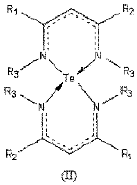
- The method of claim 2, wherein the germanium- and tellurium-containing film further comprises antimony, said method comprising volatilizing an antimony precursor to form an antimony precursor vapor, and contacting the antimony precursor vapor with the substrate for vapor deposition of the film thereon.
- The method of claim 4, wherein the antimony precursor is selected from the group consisting of antimony compositions of the formulae:
Sb(NR1R2)(R3N(CR6)mNR4)
wherein:R1, R2, R3, and R4 may be the same as or different from one another, and are independently selected from C1-C6 alkyl, C3-C6 cycloalkyl, C2-C6 alkenyl, C3-C6 alkylsilyl, C6-C10 aryl,each of R5 and R6 may be the same as or different from one another and are independently selected from hydrogen, C1-C6 alkyl, C3-C6 cycloalkyl, C2-C6 alkenyl (e.g., vinyl, allyl, etc.), C3-C6 alkylsilyl, and C6-C10 aryl; andm is an integer from 1 to 4 inclusive;wherein:
Sb(R1)(R2N(CR4R5)mNR3)
R1, R2, and R3 may be the same as or different from one another, and are independently selected from C1-C6 alkyl, C3-C6 cycloalkyl, C2-C6 alkenyl (e.g., vinyl, allyl, etc.), C3-C6 alkylsilyl, and C6-C10 aryl;each of R4 and R5 may be the same as or different from one another and is independently selected from hydrogen, C1-C6 alkyl, C3-C6 cycloalkyl, C2-C6 alkenyl (e.g., vinyl, allyl, etc.), C3-C6 alkylsilyl, and C6-C10 aryl; andm is an integer from 1 to 4 inclusive;wherein:
Sb(R1)3-n(NR2R3)n
R1, R2 and R3 may be the same as or different from one another and are independently selected from hydrogen, C1-C6 alkyl, C3-C6 cycloalkyl, C2-C6 alkenyl (e.g., vinyl, allyl, etc.), silyl, C3-C6 alkylsilyl, C6-C10 aryl and -NR4R5, wherein each of R4 and R5 is selected from among H and C1-C4; andn is an integer from 0 to 3 inclusive.wherein:
(R4)nSb(E(R1R2R3))3-n
R1, R2, R3, and R4 may be the same as or different from one another, and are independently selected from C1-C6 alkyl, C3-C6 cycloalkyl, C3-C6 alylsilyl, C6-C10 aryl, and alkylamino of the formula -NR5R6 wherein each of R5 and R6 is independently selected from H and C1-C4 alkyl;E is silicon (Si) or germanium (Ge); andn is an integer from 0 to 3 inclusive;aminidates, guanidates and isoureates of the formula:where each R1 and R2 is independently selected from among H, C1-C6 alkyl, C5-C10 cycloalkyl, C6-C10 aryl, and -Si(R3)3 wherein each R3 is independently selected from C1-C6 alkyl;
R7 nSb[R1NC(X)NR2]3-n
each X is independently selected from among C1-C6 alkoxy, -NR4R5, and -C(R6)3, wherein each of R4, R5 and R6 is independently selected from H, C1-C6 alkyl, C5-C10 cycloalkyl, C6-C10 aryl, and -Si(R3)3 wherein each R3 is independently selected from C1-C6 alkyl;
each R7 is independently selected from among C1-C6 alkoxy, -NR8R9, and -C(R10)3, wherein each of R8, R9 and R10 is independently selected from H, C1-C6 alkyl, C5-C10 cycloalkyl, C6-C10 aryl, -Si(R3)3, and -Ge(R3)3 wherein each R3 is independently selected from C1-C6 alkyl; and
n is an integer from 0 to 3;
tetra-alkyl guanidates of the formula:
R5 nSb[(R1R2)NC(NR3R4)N)]3-n
wherein:each of R1 and R2 is independently selected from among H, C1-C6 alkyl, C5-C10 cycloalkyl, C6-C10 aryl, and -Si(R9)3 wherein each R9 is independently selected from C1-C6 alkyl;each of R3 and R4 is independently selected from H, C1-C6 alkyl, C5-C10 cycloalkyl, C6-C10 aryl, and -Si(R9)3 wherein each R9 is independently selected from C1-C6 alkyl;each R5 is independently selected from among C1-C6 alkoxy, -NR6R7, and -C(R8)3, wherein each of R6, R7 and R8 is independently selected from H, C1-C6 alkyl, C5-C10 cycloalkyl, C6-C10 aryl, -Si(R9)3, and -Ge(R9)3 wherein each R9 is independently selected from C1-C6 alkyl; andn is an integer from 0 to 3;carbamates and thiocarbamates of the formula:wherein:
R4 nSb[(EC(X)E]3-n
each X is independently selected from among C1-C6 alkoxy, ―NR1R2, and -C(R3)3, wherein each of R1, R2 and R3 is independently selected from H, C1-C6 alkyl, C5-C10 cycloalkyl, C6-C10 aryl, and -Si(R5)3 wherein each R5 is independently selected from C1-C6 alkyl;each R4 is independently selected from among C1-C6 alkoxy, ―NR1R2, and -C(R3)3, wherein each of R1, R2 and R3 is independently selected from H, C1-C6 alkyl, C5-C10 cycloalkyl, C6-C10 aryl, and -Si(R5)3, -Ge(R5)3 wherein each R5 is independently selected from C1-C6 alkyl;E is either O or S; andn is an integer from 0 to 3;beta-diketonates, diketoiminates, and diketiiminates, of the formulae:
[OC(R3)C(X)C(R2)O]3-nSb(R5)n
[OC(R3)C(X)C(R2)N(R1)]3-nSb(R5)n
[R4NC(R3)C(X)C(R2)N(R1)]3-nSb(R5)n
[(R3)OC(=O)C(X)C(R2)S]3-nSb(R5)n
where each of R1,R2, R3 and R4 is independently selected from among H, C1-C6 alkyl, C5-C10 cycloalkyl, C6-C10 aryl, and -Si(R6)3 wherein each R6 is independently selected from C1-C6 alkyl;
each X is independently selected from among C1-C6 alkoxy, -NR6R7, and -C(R8)3, wherein each of R6, R7 and R8 is independently selected from H, C1-C6 alkyl, C5-C10 cycloalkyl, C6-C10 aryl, and -Si(R6)3 wherein each R6 is independently selected from C1-C6 alkyl;
each R5 is independently selected from among guanidinate, aminidate, isoureate, allyl, C1-C6 alkoxy, ―NR9R10, and -C(R11)3, wherein each of R9, R10 and R11 is independently selected from H, C1-C6 alkyl, C5-C10 cycloalkyl, C6-C10 aryl, -Si(R6)3, and - Ge(R6)3 wherein each R6 is independently selected from C1-C6 alkyl; and
n is an integer from 0 to 3.
allyls of the formulae:
R4 nSb[R1NC(X)C(R2R3)]3-n (i):
R4 nSb[(R1O)NC(X)C(R2R3))]3-n (ii):
R4 nSb[(R1R5)NC(X)C(R2R3))3-n (iii):
R4Sb[(ONC(X)C(R2R3))] (iv):
where each R1,R2, R3 and R5 is independently selected from among H, C1-C6 alkyl, C5-C10 cycloalkyl, C6-C10 aryl, and -Si(R6)3 wherein each R6 is independently selected from C1-C6 alkyl;
each X is independently selected from among C1-C6 alkoxy, ―NR1R2, and -C(R3)3, wherein each of R1, R2 and R3 is independently selected from H, C1-C6 alkyl, C5-C10 cycloalkyl, C6-C10 aryl, and -Si(R6)3 wherein each R6 is independently selected from C1-C6 alkyl;
each R4 is independently selected from among guanidinates, aminidates, isoureates, beta-diketonates, diketoiminates, diketiiminates, C1-C6 alkoxy, ―NR7R8, and -C(R9)3, wherein each of R7, R8 and R9 is independently selected from H, C1-C6 alkyl, C5-C10 cycloalkyl, C6-C10 aryl, -Si(R6)3, and -Ge(R6)3 wherein each R6 is independently selected from C1-C6 alkyl; and
n is an integer from 0 to 3;
cyclopentadienyl (Cp) antimony compounds wherein the Cp moiety is of the formulae:


wherein: the methylene (-CH2-) moiety could alternatively be another divalent hydrocarbyl moiety; each of R1-R4 is the same as or different from one another, with each being independently selected from among hydrogen, C1-C6 alkyl and C6-C10 aryl; each of R5 and R6 is the same as or different from the other, with each being independently selected from among C1-C6 alkyl; n and m are each selected independently as having a value of from 0 to 4, with the proviso that m and n cannot be 0 at the same time, and x is selected from 1 to 5;
wherein each of R1-R4 is the same as or different from one another, with each being independently selected from among hydrogen, C1-C6 alkyl, and C6-C10 aryl; R5 is selected from among C1-C6 alkyl, and C6-C10 aryl; and n and m are selected independently as having a value of from 0 to 4, with the proviso that m and n cannot be 0 at the same time;

wherein each of R1, R2, R3, R4, R5 is the same as or different from one another, with each being independently selected from among hydrogen, C1-C6 alkyl, and C6-C10 aryl; each of R1', R2' is the same as or different from one another, with each being independently selected from C1-C6 alkyl, and C6-C10 aryl; and n and m are selected independently from 0 to 4, with the proviso that m and n cannot be 0 at the same time;
wherein each of R1-R4 is the same as or different from one another, with each being independently selected from among hydrogen, C1-C6 alkyl, and C6-C10 aryl; R5 is selected from among C1-C6 alkyl, C6-C10 aryl, and C1-C5 alkoxy; and n and m are selected independently from 0 to 4, with the proviso that m and n cannot be 0 at the same time;
wherein non-Cp ligand(s) of the antimony Cp compound can optionally include ligands selected from the group consisting of guanidinates, aminidates, isoureates, allyls, beta-diketonates, diketoiminates, and diketiiminates; and
(M) alkyls, alkoxides and silyls with pendent ligands, of the formulae:
R5 nSb[(R1R2)N(CH2)mC(R1R2)]3-n (i):
R5 nSb[(R1R2)N(CH2)mSi(R1R2)]3-n (ii):
: R5 nSb[(R1R2)N(CH2)mO]3-n (iii)
where each of R1 and R2 is independently selected from among H, C1-C6 alkyl, C5-C10 cycloalkyl, C6-C10 aryl, and -Si(R3)3 wherein each R3 is independently selected from C1-C6 alkyl;
each R5 is independently selected from among guanidinates, aminidates, isoureates, beta-diketonates, diketoiminates, diketiiminates, C1-C6 alkoxy, ―NR6R7, and -C(R8)3, wherein each of R6, R7 and R8 is independently selected from H, C1-C6 alkyl, C5-C10 cycloalkyl, C6-C10 aryl, -Si(R3)3, and -Ge(R3)3 wherein each R3 is independently selected from C1-C6 alkyl;
n is an integer from 0 to 3;
m is integer from 0 to 4.


- The method of claim 1, comprising combining the precursor vapor with a component selected from the group consisting of ammonia, hydrogen, helium, argon, and nitrogen.
- The method of claim 1, wherein the substrate is also contacted with precursor vapor of an antimony precursor and with precursor vapor of a tellurium precursor, so that the germanium-containing film comprises a GeSbTe film, and wherein the method is carried out so as to combat precursor pre-reaction of at least one of said germanium, antimony and tellurium precursors.
- The method of claim 1, wherein the film is a smooth, amorphous GeTe or a GeSbTe film.
- The method of claim 2, wherein the tellurium precursor comprises a dialkyl tellurium compound selected from among di-tert-butyl tellurium and diisopropyl tellurium.
- The method of claim 1, wherein said film is deposited in a fill trench or via structure on the substrate.
- The method of claim 1, comprising forming a phase change random access memory device including a germanium- and tellurium-containing film of smooth, amorphous character.
- The method of claim 1, comprising combating pre-reaction of precursor by introducing to said process a pre-reaction-combating agent selected from the group consisting of (i) (O, N, S) organo Lewis base compounds, (ii) free radical inhibitors, and (iii) deuterium-containing reagents.
- The method of claim 1, for forming a smooth amorphous germanium telluride film, comprising volatilizing the germanium precursor and a diakyl tellurium precursor to form the precursor vapor and contacting the precursor vapor with the substrate to form the smooth amorphous germanium telluride film on the substrate.
- The method of claim 1, for forming a phase change random access memory device, comprising forming a germanium telluride film of smooth, amorphous character, including vapor deposition of germanium from said germanium precursor, wherein said vapor deposition comprises use of a dialkyl tellurium precursor, and is carried out with a co-reactant comprising ammonia.
- The method of claim 1, wherein said germanium precursor is contacted with said substrate in manufacturing a phase change random access memory device.
Applications Claiming Priority (6)
| Application Number | Priority Date | Filing Date | Title |
|---|---|---|---|
| US98437007P | 2007-10-31 | 2007-10-31 | |
| US12/076,428 US20090017275A1 (en) | 2007-07-09 | 2008-03-18 | Heat-releasing printed circuit board and manufacturing method thereof |
| US5017908P | 2008-05-02 | 2008-05-02 | |
| US5127408P | 2008-05-07 | 2008-05-07 | |
| US5201808P | 2008-05-09 | 2008-05-09 | |
| US7642808P | 2008-06-27 | 2008-06-27 |
Related Parent Applications (1)
| Application Number | Title | Priority Date | Filing Date |
|---|---|---|---|
| EP08019157.0 Division | 2008-10-31 |
Publications (1)
| Publication Number | Publication Date |
|---|---|
| EP2479313A1 true EP2479313A1 (en) | 2012-07-25 |
Family
ID=40583707
Family Applications (2)
| Application Number | Title | Priority Date | Filing Date |
|---|---|---|---|
| EP20120164278 Withdrawn EP2479313A1 (en) | 2007-10-31 | 2008-10-31 | Amorphous Ge/Te deposition process |
| EP20080019157 Not-in-force EP2062995B1 (en) | 2007-10-31 | 2008-10-31 | Amorphous Ge/Te deposition process |
Family Applications After (1)
| Application Number | Title | Priority Date | Filing Date |
|---|---|---|---|
| EP20080019157 Not-in-force EP2062995B1 (en) | 2007-10-31 | 2008-10-31 | Amorphous Ge/Te deposition process |
Country Status (7)
| Country | Link |
|---|---|
| US (2) | US8093140B2 (en) |
| EP (2) | EP2479313A1 (en) |
| JP (1) | JP5650880B2 (en) |
| KR (1) | KR101065829B1 (en) |
| CN (2) | CN102912314B (en) |
| SG (2) | SG152203A1 (en) |
| TW (1) | TWI477641B (en) |
Families Citing this family (52)
| Publication number | Priority date | Publication date | Assignee | Title |
|---|---|---|---|---|
| SG171683A1 (en) | 2006-05-12 | 2011-06-29 | Advanced Tech Materials | Low temperature deposition of phase change memory materials |
| EP2511280A1 (en) | 2006-11-02 | 2012-10-17 | Advanced Technology Materials, Inc. | Germanium amidinate complexes useful for CVD/ALD of metal thin films |
| KR101275799B1 (en) * | 2006-11-21 | 2013-06-18 | 삼성전자주식회사 | Method of forming phase change layer using Ge precursor for low temperature deposition and method of manufacturing phase change memory device using the same |
| WO2008088563A2 (en) * | 2007-01-17 | 2008-07-24 | Advanced Technology Materials, Inc. | Precursor compositions for ald/cvd of group ii ruthenate thin films |
| US20100112211A1 (en) * | 2007-04-12 | 2010-05-06 | Advanced Technology Materials, Inc. | Zirconium, hafnium, titanium, and silicon precursors for ald/cvd |
| US9337054B2 (en) * | 2007-06-28 | 2016-05-10 | Entegris, Inc. | Precursors for silicon dioxide gap fill |
| KR101458953B1 (en) * | 2007-10-11 | 2014-11-07 | 삼성전자주식회사 | Method of forming phase change material layer using Ge(Ⅱ) source, and method of fabricating phase change memory device |
| US8834968B2 (en) | 2007-10-11 | 2014-09-16 | Samsung Electronics Co., Ltd. | Method of forming phase change material layer using Ge(II) source, and method of fabricating phase change memory device |
| US20100279011A1 (en) * | 2007-10-31 | 2010-11-04 | Advanced Technology Materials, Inc. | Novel bismuth precursors for cvd/ald of thin films |
| US8318252B2 (en) * | 2008-01-28 | 2012-11-27 | Air Products And Chemicals, Inc. | Antimony precursors for GST films in ALD/CVD processes |
| US20090215225A1 (en) | 2008-02-24 | 2009-08-27 | Advanced Technology Materials, Inc. | Tellurium compounds useful for deposition of tellurium containing materials |
| JP5718808B2 (en) | 2008-04-25 | 2015-05-13 | エーエスエム インターナショナル エヌ.ヴェー.Asm International N.V. | Synthesis and use of precursors for ALD of tellurium and selenium thin films |
| WO2009134989A2 (en) * | 2008-05-02 | 2009-11-05 | Advanced Technology Materials, Inc. | Antimony compounds useful for deposition of antimony-containing materials |
| US20090275164A1 (en) * | 2008-05-02 | 2009-11-05 | Advanced Technology Materials, Inc. | Bicyclic guanidinates and bridging diamides as cvd/ald precursors |
| US8765223B2 (en) * | 2008-05-08 | 2014-07-01 | Air Products And Chemicals, Inc. | Binary and ternary metal chalcogenide materials and method of making and using same |
| US8507040B2 (en) * | 2008-05-08 | 2013-08-13 | Air Products And Chemicals, Inc. | Binary and ternary metal chalcogenide materials and method of making and using same |
| WO2009152108A2 (en) * | 2008-06-10 | 2009-12-17 | Advanced Technology Materials, Inc. | GeSbTe MATERIAL INCLUDING SUPERFLOW LAYER(S), AND USE OF Ge TO PREVENT INTERACTION OF Te FROM SbXTeY AND GeXTeY RESULTING IN HIGH Te CONTENT AND FILM CRISTALLINITY |
| US8636845B2 (en) | 2008-06-25 | 2014-01-28 | L'Air Liquide, Société Anonyme pour l'Etude et l'Exploitation des Procédés Georges Claude | Metal heterocyclic compounds for deposition of thin films |
| US8168811B2 (en) * | 2008-07-22 | 2012-05-01 | Advanced Technology Materials, Inc. | Precursors for CVD/ALD of metal-containing films |
| US8236381B2 (en) * | 2008-08-08 | 2012-08-07 | L'air Liquide Societe Anonyme Pour L'etude Et L'exploitation Des Procedes Georges Claude | Metal piperidinate and metal pyridinate precursors for thin film deposition |
| WO2010065874A2 (en) | 2008-12-05 | 2010-06-10 | Atmi | High concentration nitrogen-containing germanium telluride based memory devices and processes of making |
| KR101120065B1 (en) * | 2009-01-08 | 2012-03-23 | 솔브레인 주식회사 | Novel germanium complexes with amidine derivative ligand and process for preparing the same |
| US8003521B2 (en) * | 2009-04-07 | 2011-08-23 | Micron Technology, Inc. | Semiconductor processing |
| US8198129B2 (en) | 2009-04-15 | 2012-06-12 | Micron Technology, Inc. | Methods of depositing antimony-comprising phase change material onto a substrate and methods of forming phase change memory circuitry |
| US8617972B2 (en) | 2009-05-22 | 2013-12-31 | Advanced Technology Materials, Inc. | Low temperature GST process |
| KR101602007B1 (en) * | 2009-07-02 | 2016-03-09 | 인티그리스, 인코포레이티드 | Hollow gst structure with dielectric fill |
| CN102687243B (en) | 2009-10-26 | 2016-05-11 | Asm国际公司 | Be used for the synthetic and use of the precursor of the film ALD that contains VA family element |
| US20110108792A1 (en) * | 2009-11-11 | 2011-05-12 | International Business Machines Corporation | Single Crystal Phase Change Material |
| US20110124182A1 (en) * | 2009-11-20 | 2011-05-26 | Advanced Techology Materials, Inc. | System for the delivery of germanium-based precursor |
| WO2011095849A1 (en) | 2010-02-03 | 2011-08-11 | L'air Liquide, Societe Anonyme Pour L'etude Et L'exploitation Des Procedes Georges Claude | Chalcogenide-containing precursors, methods of making, and methods of using the same for thin film deposition |
| KR20110095040A (en) * | 2010-02-18 | 2011-08-24 | 삼성전자주식회사 | Apparatus and method of fabricating phase change material |
| US9012876B2 (en) | 2010-03-26 | 2015-04-21 | Entegris, Inc. | Germanium antimony telluride materials and devices incorporating same |
| US9190609B2 (en) | 2010-05-21 | 2015-11-17 | Entegris, Inc. | Germanium antimony telluride materials and devices incorporating same |
| JP5572447B2 (en) * | 2010-05-25 | 2014-08-13 | 株式会社日立国際電気 | Semiconductor device manufacturing method, substrate processing method, and substrate processing apparatus |
| US8124445B2 (en) | 2010-07-26 | 2012-02-28 | Micron Technology, Inc. | Confined resistance variable memory cell structures and methods |
| US8148197B2 (en) | 2010-07-27 | 2012-04-03 | Micron Technology, Inc. | Methods of forming germanium-antimony-tellurium materials and a method of forming a semiconductor device structure including the same |
| TWI452167B (en) * | 2011-06-09 | 2014-09-11 | Air Prod & Chem | Binary and ternary metal chalcogenide materials and method of making and using same |
| WO2013027682A1 (en) * | 2011-08-19 | 2013-02-28 | 東京エレクトロン株式会社 | Method for forming ge-sb-te film, method for forming ge-te film, method for forming sb-te film, and program |
| US8741688B2 (en) | 2012-07-24 | 2014-06-03 | Micron Technology, Inc. | Methods of forming a metal chalcogenide material |
| US9640757B2 (en) | 2012-10-30 | 2017-05-02 | Entegris, Inc. | Double self-aligned phase change memory device structure |
| KR102022409B1 (en) | 2013-03-13 | 2019-09-18 | 삼성전자주식회사 | Method of forming a thin layer and method of manufacturing a phase-change memory device using the same |
| US9214630B2 (en) | 2013-04-11 | 2015-12-15 | Air Products And Chemicals, Inc. | Method of making a multicomponent film |
| JP6153895B2 (en) | 2013-07-22 | 2017-06-28 | 富士フイルム株式会社 | Liquid crystal display |
| EP3114248A4 (en) * | 2014-03-04 | 2017-03-01 | Picosun Oy | Atomic layer deposition of germanium or germanium oxide |
| WO2015145746A1 (en) * | 2014-03-28 | 2015-10-01 | 株式会社日立製作所 | Method for vapor-phase growth of phase-change thin film, and device for vapor-phase growth of phase-change thin film |
| GB201412201D0 (en) * | 2014-07-09 | 2014-08-20 | Isis Innovation | Two-step deposition process |
| CN104086589B (en) * | 2014-07-17 | 2017-02-01 | 江南大学 | Easily prepared pyrazolyl Ge (II) compound used as microelectronic material |
| KR101952729B1 (en) * | 2016-04-29 | 2019-02-27 | 세종대학교산학협력단 | Preparing method of chalcogen-containing film using atomic layer deposition |
| FR3058162B1 (en) * | 2016-11-02 | 2021-01-01 | Commissariat Energie Atomique | DEPOSIT PROCESS FOR THIN CHALCOGENURE FILMS |
| US10964536B2 (en) * | 2019-02-06 | 2021-03-30 | Micron Technology, Inc. | Formation of an atomic layer of germanium in an opening of a substrate material having a high aspect ratio |
| CN110010178B (en) * | 2019-03-27 | 2020-10-30 | 华中科技大学 | Two-dimensional GeTe single crystal nanosheet and application thereof in phase change storage |
| US11319449B2 (en) * | 2019-12-20 | 2022-05-03 | L'Air Liquide, Société Anonyme pour l'Etude et l'Exploitation des Procédés Georges Claude | Area selective deposition of metal containing films |
Citations (2)
| Publication number | Priority date | Publication date | Assignee | Title |
|---|---|---|---|---|
| US20060138393A1 (en) * | 2004-12-27 | 2006-06-29 | Samsung Electronics Co., Ltd. | Ge precursor, GST thin layer formed using the same, phase-change memory device including the GST thin layer, and method of manufacturing the GST thin layer |
| WO2008057616A2 (en) * | 2006-11-02 | 2008-05-15 | Advanced Technology Materials, Inc. | Antimony and germanium complexes useful for cvd/ald of metal thin films |
Family Cites Families (98)
| Publication number | Priority date | Publication date | Assignee | Title |
|---|---|---|---|---|
| US6013A (en) * | 1849-01-09 | Improvement in molding and compressing cores | ||
| SU768457A1 (en) | 1976-01-04 | 1980-10-07 | Всесоюзный научно-исследовательский и проектно-конструкторский институт добычи угля гидравлическим способом | Catalyst for removing nitrogen oxides from exhaust gases |
| JPS5838296A (en) | 1981-08-31 | 1983-03-05 | Ichiro Kijima | Novel antimony compound |
| US4710478A (en) * | 1985-05-20 | 1987-12-01 | United States Of America As Represented By The Secretary Of The Navy | Method for making germanium/gallium arsenide high mobility complementary logic transistors |
| US4948623A (en) | 1987-06-30 | 1990-08-14 | International Business Machines Corporation | Method of chemical vapor deposition of copper, silver, and gold using a cyclopentadienyl/metal complex |
| US4962214A (en) | 1988-05-11 | 1990-10-09 | Massachusettes Institute Of Technology | Catalytic enantioselective addition of hydrocarbon equivalents to alpha, beta-unsaturated carbonyl compounds |
| US4927670A (en) | 1988-06-22 | 1990-05-22 | Georgia Tech Research Corporation | Chemical vapor deposition of mixed metal oxide coatings |
| US4960916A (en) | 1989-09-29 | 1990-10-02 | United States Of America As Represented By The Secretary Of The Navy | Organometallic antimony compounds useful in chemical vapor deposition processes |
| US5453494A (en) | 1990-07-06 | 1995-09-26 | Advanced Technology Materials, Inc. | Metal complex source reagents for MOCVD |
| US5296716A (en) | 1991-01-18 | 1994-03-22 | Energy Conversion Devices, Inc. | Electrically erasable, directly overwritable, multibit single cell memory elements and arrays fabricated therefrom |
| US5596522A (en) | 1991-01-18 | 1997-01-21 | Energy Conversion Devices, Inc. | Homogeneous compositions of microcrystalline semiconductor material, semiconductor devices and directly overwritable memory elements fabricated therefrom, and arrays fabricated from the memory elements |
| US5359205A (en) * | 1991-11-07 | 1994-10-25 | Energy Conversion Devices, Inc. | Electrically erasable memory elements characterized by reduced current and improved thermal stability |
| US5997642A (en) | 1996-05-21 | 1999-12-07 | Symetrix Corporation | Method and apparatus for misted deposition of integrated circuit quality thin films |
| CN1253597A (en) * | 1997-03-11 | 2000-05-17 | 阿尔·阿尔马格公司 | Process and apparatus for coating metals |
| US6146608A (en) | 1997-11-24 | 2000-11-14 | Advanced Technology Materials, Inc. | Stable hydride source compositions for manufacture of semiconductor devices and structures |
| US6005127A (en) | 1997-11-24 | 1999-12-21 | Advanced Technology Materials, Inc. | Antimony/Lewis base adducts for Sb-ion implantation and formation of antimonide films |
| US6787186B1 (en) | 1997-12-18 | 2004-09-07 | Advanced Technology Materials, Inc. | Method of controlled chemical vapor deposition of a metal oxide ceramic layer |
| US7098163B2 (en) | 1998-08-27 | 2006-08-29 | Cabot Corporation | Method of producing membrane electrode assemblies for use in proton exchange membrane and direct methanol fuel cells |
| US6123993A (en) | 1998-09-21 | 2000-09-26 | Advanced Technology Materials, Inc. | Method and apparatus for forming low dielectric constant polymeric films |
| US6086779A (en) | 1999-03-01 | 2000-07-11 | Mcgean-Rohco, Inc. | Copper etching compositions and method for etching copper |
| JP2001067720A (en) | 1999-08-31 | 2001-03-16 | Toray Ind Inc | Optical recording medium |
| US6269979B1 (en) | 1999-10-05 | 2001-08-07 | Charles Dumont | Multi-compartmented mixing dispenser |
| GB0004852D0 (en) | 2000-02-29 | 2000-04-19 | Unilever Plc | Ligand and complex for catalytically bleaching a substrate |
| US20020013487A1 (en) | 2000-04-03 | 2002-01-31 | Norman John Anthony Thomas | Volatile precursors for deposition of metals and metal-containing films |
| US6984591B1 (en) | 2000-04-20 | 2006-01-10 | International Business Machines Corporation | Precursor source mixtures |
| JP4621333B2 (en) | 2000-06-01 | 2011-01-26 | ホーチキ株式会社 | Thin film formation method |
| US20020090815A1 (en) | 2000-10-31 | 2002-07-11 | Atsushi Koike | Method for forming a deposited film by plasma chemical vapor deposition |
| CN1134051C (en) * | 2000-12-19 | 2004-01-07 | 中国科学院微电子中心 | Method for generating extended super-shallow source-drain region by combining amorphous pre-injection of Ge with low energy injection |
| US7087482B2 (en) | 2001-01-19 | 2006-08-08 | Samsung Electronics Co., Ltd. | Method of forming material using atomic layer deposition and method of forming capacitor of semiconductor device using the same |
| US7005392B2 (en) | 2001-03-30 | 2006-02-28 | Advanced Technology Materials, Inc. | Source reagent compositions for CVD formation of gate dielectric thin films using amide precursors and method of using same |
| US6507061B1 (en) | 2001-08-31 | 2003-01-14 | Intel Corporation | Multiple layer phase-change memory |
| CN100379745C (en) | 2001-10-26 | 2008-04-09 | 埃普切公司 | Improved precursors for chemical vapour deposition |
| US6872963B2 (en) | 2002-08-08 | 2005-03-29 | Ovonyx, Inc. | Programmable resistance memory element with layered memory material |
| EP1563117B1 (en) | 2002-11-15 | 2010-01-06 | President And Fellows Of Harvard College | Atomic layer deposition using metal amidinates |
| US6861559B2 (en) | 2002-12-10 | 2005-03-01 | Board Of Trustees Of Michigan State University | Iminoamines and preparation thereof |
| US7402851B2 (en) | 2003-02-24 | 2008-07-22 | Samsung Electronics Co., Ltd. | Phase changeable memory devices including nitrogen and/or silicon and methods for fabricating the same |
| US7115927B2 (en) | 2003-02-24 | 2006-10-03 | Samsung Electronics Co., Ltd. | Phase changeable memory devices |
| US7425735B2 (en) | 2003-02-24 | 2008-09-16 | Samsung Electronics Co., Ltd. | Multi-layer phase-changeable memory devices |
| JP4714422B2 (en) | 2003-04-05 | 2011-06-29 | ローム・アンド・ハース・エレクトロニック・マテリアルズ,エル.エル.シー. | Method for depositing germanium-containing film and vapor delivery device |
| US20040215030A1 (en) | 2003-04-22 | 2004-10-28 | Norman John Anthony Thomas | Precursors for metal containing films |
| US7029978B2 (en) | 2003-08-04 | 2006-04-18 | Intel Corporation | Controlling the location of conduction breakdown in phase change memories |
| US20050082624A1 (en) | 2003-10-20 | 2005-04-21 | Evgeni Gousev | Germanate gate dielectrics for semiconductor devices |
| US7005665B2 (en) | 2004-03-18 | 2006-02-28 | International Business Machines Corporation | Phase change memory cell on silicon-on insulator substrate |
| US7312165B2 (en) | 2004-05-05 | 2007-12-25 | Jursich Gregory M | Codeposition of hafnium-germanium oxides on substrates used in or for semiconductor devices |
| US7166732B2 (en) | 2004-06-16 | 2007-01-23 | Advanced Technology Materials, Inc. | Copper (I) compounds useful as deposition precursors of copper thin films |
| WO2006012052A2 (en) | 2004-06-25 | 2006-02-02 | Arkema, Inc. | Amidinate ligand containing chemical vapor deposition precursors |
| US20050287747A1 (en) | 2004-06-29 | 2005-12-29 | International Business Machines Corporation | Doped nitride film, doped oxide film and other doped films |
| KR100639206B1 (en) | 2004-06-30 | 2006-10-30 | 주식회사 하이닉스반도체 | Phase-change memory device and method for manufacturing the same |
| KR100642635B1 (en) | 2004-07-06 | 2006-11-10 | 삼성전자주식회사 | Semiconductor integrated circuit devices having a hybrid dielectric layer and methods of fabricating the same |
| KR100632948B1 (en) | 2004-08-06 | 2006-10-11 | 삼성전자주식회사 | Sputtering method for forming a chalcogen compound and method for fabricating phase-changeable memory device using the same |
| US7300873B2 (en) * | 2004-08-13 | 2007-11-27 | Micron Technology, Inc. | Systems and methods for forming metal-containing layers using vapor deposition processes |
| US20060110930A1 (en) * | 2004-08-16 | 2006-05-25 | Yoshihide Senzaki | Direct liquid injection system and method for forming multi-component dielectric films |
| KR100652378B1 (en) | 2004-09-08 | 2006-12-01 | 삼성전자주식회사 | Sb Precursor and Manufacturing Method of Phase-Change Memory Device using the Same |
| US7390360B2 (en) | 2004-10-05 | 2008-06-24 | Rohm And Haas Electronic Materials Llc | Organometallic compounds |
| JP2006156886A (en) | 2004-12-01 | 2006-06-15 | Renesas Technology Corp | Semiconductor integrated circuit device and manufacturing method therefor |
| US20060172067A1 (en) * | 2005-01-28 | 2006-08-03 | Energy Conversion Devices, Inc | Chemical vapor deposition of chalcogenide materials |
| US20080286446A1 (en) | 2005-01-28 | 2008-11-20 | Smuruthi Kamepalli | Seed-Assisted MOCVD Growth of Threshold Switching and Phase-Change Materials |
| KR100585175B1 (en) | 2005-01-31 | 2006-05-30 | 삼성전자주식회사 | Fabrication method of gesbte thin film by chemical vapor deposition process |
| KR100688532B1 (en) | 2005-02-14 | 2007-03-02 | 삼성전자주식회사 | A Te precursor, a Te-including chalcogenide thin layer prepared by using the Te precursor, a method for preparing the thin layer and a phase-change memory device |
| US7399666B2 (en) | 2005-02-15 | 2008-07-15 | Micron Technology, Inc. | Atomic layer deposition of Zr3N4/ZrO2 films as gate dielectrics |
| KR100681266B1 (en) | 2005-07-25 | 2007-02-09 | 삼성전자주식회사 | Method of manufacturing a variable resistance and method of manufacturing a phase changeable memory device using the same |
| DE102006038885B4 (en) * | 2005-08-24 | 2013-10-10 | Wonik Ips Co., Ltd. | Method for depositing a Ge-Sb-Te thin film |
| KR100962623B1 (en) | 2005-09-03 | 2010-06-11 | 삼성전자주식회사 | Method of forming a phase changeable material layer, and methods of manufacturing a phase changeable memory unit and a phase changeable memory device using the same |
| KR100675289B1 (en) | 2005-11-14 | 2007-01-29 | 삼성전자주식회사 | Phase changeable memory cell array region and methods of forming the same |
| US7459717B2 (en) | 2005-11-28 | 2008-12-02 | Macronix International Co., Ltd. | Phase change memory cell and manufacturing method |
| WO2007067604A2 (en) | 2005-12-06 | 2007-06-14 | Structured Materials Inc. | Method of making undoped, alloyed and doped chalcogenide films by mocvd processes |
| US20070154637A1 (en) | 2005-12-19 | 2007-07-05 | Rohm And Haas Electronic Materials Llc | Organometallic composition |
| KR100695168B1 (en) | 2006-01-10 | 2007-03-14 | 삼성전자주식회사 | Method of forming phase change material thin film, and method of manufacturing phase change memory device using the same |
| SG171683A1 (en) | 2006-05-12 | 2011-06-29 | Advanced Tech Materials | Low temperature deposition of phase change memory materials |
| EP2029790A1 (en) | 2006-06-02 | 2009-03-04 | L'AIR LIQUIDE, Société Anonyme pour l'Etude et l'Exploitation des Procédés Georges Claude | Method of forming high-k dielectric films based on novel titanium, zirconium, and hafnium precursors and their use for semiconductor manufacturing |
| US7638645B2 (en) | 2006-06-28 | 2009-12-29 | President And Fellows Of Harvard University | Metal (IV) tetra-amidinate compounds and their use in vapor deposition |
| WO2008002546A1 (en) | 2006-06-28 | 2008-01-03 | President And Fellows Of Harvard College | Metal(iv) tetra-amidinate compounds and their use in vapor deposition |
| KR100780865B1 (en) | 2006-07-19 | 2007-11-30 | 삼성전자주식회사 | Methods of forming a semiconductor device including a phase-change layer |
| KR100791477B1 (en) | 2006-08-08 | 2008-01-03 | 삼성전자주식회사 | A phase-change memory unit, method of manufacturing the phase-change memory unit, a phase-change memory device having the phase-change memory unit and method of manufacturing the phase-change memory device |
| KR101263822B1 (en) | 2006-10-20 | 2013-05-13 | 삼성전자주식회사 | Method of manufacturing phase change memory device and method of forming phase change layer applied in the same |
| KR101275799B1 (en) | 2006-11-21 | 2013-06-18 | 삼성전자주식회사 | Method of forming phase change layer using Ge precursor for low temperature deposition and method of manufacturing phase change memory device using the same |
| KR20080055508A (en) | 2006-12-15 | 2008-06-19 | 삼성전자주식회사 | Phase change layer having different crystal lattice in single layer and method of forming the same and phase change memory device comprising means for preventing ti diffusion and method of manufacturing the same |
| KR100896180B1 (en) | 2007-01-23 | 2009-05-12 | 삼성전자주식회사 | Phase change Random Access Memory comprising phase change material layer formed by selective growth method and method of manufacturing the same |
| EP2142682B1 (en) | 2007-04-09 | 2014-12-03 | President and Fellows of Harvard College | Cobalt nitride layers for copper interconnects and methods for forming them |
| US20080254218A1 (en) | 2007-04-16 | 2008-10-16 | Air Products And Chemicals, Inc. | Metal Precursor Solutions For Chemical Vapor Deposition |
| US8377341B2 (en) | 2007-04-24 | 2013-02-19 | Air Products And Chemicals, Inc. | Tellurium (Te) precursors for making phase change memory materials |
| US20080272355A1 (en) | 2007-05-04 | 2008-11-06 | Samsung Electronics Co., Ltd. | Phase change memory device and method for forming the same |
| US7659414B2 (en) * | 2007-07-20 | 2010-02-09 | Rohm And Haas Company | Method of preparing organometallic compounds |
| KR20090013419A (en) | 2007-08-01 | 2009-02-05 | 삼성전자주식회사 | Phase change memory devices and methods of forming the same |
| KR101370275B1 (en) | 2007-08-21 | 2014-03-05 | 삼성전자주식회사 | Phase Change Random Access Memory and Manufacturing Method for the Same |
| US8454928B2 (en) | 2007-09-17 | 2013-06-04 | L'air Liquide Societe Anonyme Pour L'etude Et L'exploitation Des Procedes Georges Claude | Tellurium precursors for GST deposition |
| KR101458953B1 (en) | 2007-10-11 | 2014-11-07 | 삼성전자주식회사 | Method of forming phase change material layer using Ge(Ⅱ) source, and method of fabricating phase change memory device |
| US7960205B2 (en) | 2007-11-27 | 2011-06-14 | Air Products And Chemicals, Inc. | Tellurium precursors for GST films in an ALD or CVD process |
| US20090162973A1 (en) | 2007-12-21 | 2009-06-25 | Julien Gatineau | Germanium precursors for gst film deposition |
| US8318252B2 (en) | 2008-01-28 | 2012-11-27 | Air Products And Chemicals, Inc. | Antimony precursors for GST films in ALD/CVD processes |
| US20090215225A1 (en) | 2008-02-24 | 2009-08-27 | Advanced Technology Materials, Inc. | Tellurium compounds useful for deposition of tellurium containing materials |
| US7935564B2 (en) | 2008-02-25 | 2011-05-03 | International Business Machines Corporation | Self-converging bottom electrode ring |
| WO2009134989A2 (en) | 2008-05-02 | 2009-11-05 | Advanced Technology Materials, Inc. | Antimony compounds useful for deposition of antimony-containing materials |
| US20090275164A1 (en) | 2008-05-02 | 2009-11-05 | Advanced Technology Materials, Inc. | Bicyclic guanidinates and bridging diamides as cvd/ald precursors |
| US8765223B2 (en) | 2008-05-08 | 2014-07-01 | Air Products And Chemicals, Inc. | Binary and ternary metal chalcogenide materials and method of making and using same |
| US8101237B2 (en) | 2008-05-29 | 2012-01-24 | L'Air Liquide SociétéAnonyme pour I'Etude et I'Exploitation des Procédés Georges Claude | Tellurium precursors for film deposition |
| US8636845B2 (en) | 2008-06-25 | 2014-01-28 | L'Air Liquide, Société Anonyme pour l'Etude et l'Exploitation des Procédés Georges Claude | Metal heterocyclic compounds for deposition of thin films |
| US20110124182A1 (en) | 2009-11-20 | 2011-05-26 | Advanced Techology Materials, Inc. | System for the delivery of germanium-based precursor |
-
2008
- 2008-10-30 SG SG200808069-9A patent/SG152203A1/en unknown
- 2008-10-30 JP JP2008279957A patent/JP5650880B2/en not_active Expired - Fee Related
- 2008-10-30 SG SG2012007159A patent/SG178736A1/en unknown
- 2008-10-31 US US12/263,403 patent/US8093140B2/en active Active
- 2008-10-31 EP EP20120164278 patent/EP2479313A1/en not_active Withdrawn
- 2008-10-31 CN CN201210337922.2A patent/CN102912314B/en not_active Expired - Fee Related
- 2008-10-31 CN CN2008101743241A patent/CN101423929B/en not_active Expired - Fee Related
- 2008-10-31 KR KR1020080108119A patent/KR101065829B1/en active IP Right Grant
- 2008-10-31 TW TW097142061A patent/TWI477641B/en active
- 2008-10-31 EP EP20080019157 patent/EP2062995B1/en not_active Not-in-force
-
2012
- 2012-01-09 US US13/346,701 patent/US20120108038A1/en not_active Abandoned
Patent Citations (2)
| Publication number | Priority date | Publication date | Assignee | Title |
|---|---|---|---|---|
| US20060138393A1 (en) * | 2004-12-27 | 2006-06-29 | Samsung Electronics Co., Ltd. | Ge precursor, GST thin layer formed using the same, phase-change memory device including the GST thin layer, and method of manufacturing the GST thin layer |
| WO2008057616A2 (en) * | 2006-11-02 | 2008-05-15 | Advanced Technology Materials, Inc. | Antimony and germanium complexes useful for cvd/ald of metal thin films |
Non-Patent Citations (4)
| Title |
|---|
| G.T. STAUF ET. AL.: "Low Temperature ALD of Germanium for Phase Change Memory Thin Films", 24 June 2007 (2007-06-24) - 27 June 2007 (2007-06-27), San Diego, California (USA), XP002522504, Retrieved from the Internet <URL:http://www2.avs.org/conferences/ALD2009/pdfs/ALD_Proceedings_Form.pdf> * |
| LEE ET AL: "GeSbTe deposition for the PRAM application", APPLIED SURFACE SCIENCE, ELSEVIER, AMSTERDAM, NL, vol. 253, no. 8, 1 February 2007 (2007-02-01), pages 3969 - 3976, XP005868235, ISSN: 0169-4332 * |
| SCHARNHORST; RIEDL: "Photoconductivity in the amorphous Ge-rich GexTel-x system", JOURNAL OF APPLIED PHYSICS, vol. 45, 1974, pages 2971 - 2979 |
| TSU, JOURNAL OF VACUUM SCIENCE & TECHNOLOGY A: VACUUM, SURFACES, AND FILMS, vol. 17, no. 4, July 1999 (1999-07-01), pages 1854 - 1860 |
Also Published As
| Publication number | Publication date |
|---|---|
| SG152203A1 (en) | 2009-05-29 |
| US20120108038A1 (en) | 2012-05-03 |
| KR20090045132A (en) | 2009-05-07 |
| US20090112009A1 (en) | 2009-04-30 |
| JP5650880B2 (en) | 2015-01-07 |
| CN101423929A (en) | 2009-05-06 |
| JP2009133003A (en) | 2009-06-18 |
| EP2062995B1 (en) | 2012-11-21 |
| CN102912314A (en) | 2013-02-06 |
| CN102912314B (en) | 2015-08-12 |
| US8093140B2 (en) | 2012-01-10 |
| SG178736A1 (en) | 2012-03-29 |
| CN101423929B (en) | 2012-11-07 |
| KR101065829B1 (en) | 2011-09-20 |
| EP2062995A1 (en) | 2009-05-27 |
| TW200938652A (en) | 2009-09-16 |
| TWI477641B (en) | 2015-03-21 |
Similar Documents
| Publication | Publication Date | Title |
|---|---|---|
| EP2062995B1 (en) | Amorphous Ge/Te deposition process | |
| US9537095B2 (en) | Tellurium compounds useful for deposition of tellurium containing materials | |
| US9034688B2 (en) | Antimony compounds useful for deposition of antimony-containing materials | |
| EP2078102B1 (en) | Antimony and germanium complexes useful for cvd/ald of metal thin films | |
| US20090275164A1 (en) | Bicyclic guanidinates and bridging diamides as cvd/ald precursors | |
| US20090087561A1 (en) | Metal and metalloid silylamides, ketimates, tetraalkylguanidinates and dianionic guanidinates useful for cvd/ald of thin films | |
| US8877549B2 (en) | Low temperature deposition of phase change memory materials | |
| US20110262660A1 (en) | Chalcogenide-containing precursors, methods of making, and methods of using the same for thin film deposition | |
| US9240319B2 (en) | Chalcogenide-containing precursors, methods of making, and methods of using the same for thin film deposition | |
| US20100279011A1 (en) | Novel bismuth precursors for cvd/ald of thin films | |
| EP2492273A1 (en) | Deposition of gallium containing thin films using gallium alkylamide precursor | |
| EP2540733A1 (en) | Deposition of indium containing thin films using new indium precursors | |
| EP2540732A1 (en) | Deposition of gallium containing thin films using new gallium precursors. |
Legal Events
| Date | Code | Title | Description |
|---|---|---|---|
| PUAI | Public reference made under article 153(3) epc to a published international application that has entered the european phase |
Free format text: ORIGINAL CODE: 0009012 |
|
| AC | Divisional application: reference to earlier application |
Ref document number: 2062995 Country of ref document: EP Kind code of ref document: P |
|
| AK | Designated contracting states |
Kind code of ref document: A1 Designated state(s): AT BE BG CH CY CZ DE DK EE ES FI FR GB GR HR HU IE IS IT LI LT LU LV MC MT NL NO PL PT RO SE SI SK TR |
|
| 17P | Request for examination filed |
Effective date: 20130124 |
|
| 17Q | First examination report despatched |
Effective date: 20130830 |
|
| STAA | Information on the status of an ep patent application or granted ep patent |
Free format text: STATUS: THE APPLICATION IS DEEMED TO BE WITHDRAWN |
|
| 18D | Application deemed to be withdrawn |
Effective date: 20140110 |