EP2473839B1 - Method for measuring a semiconductor structure, which is a solar cell or a precursor of a solar cell - Google Patents
Method for measuring a semiconductor structure, which is a solar cell or a precursor of a solar cell Download PDFInfo
- Publication number
- EP2473839B1 EP2473839B1 EP10744690.8A EP10744690A EP2473839B1 EP 2473839 B1 EP2473839 B1 EP 2473839B1 EP 10744690 A EP10744690 A EP 10744690A EP 2473839 B1 EP2473839 B1 EP 2473839B1
- Authority
- EP
- European Patent Office
- Prior art keywords
- voltage
- measurement
- spatially resolved
- exp
- semiconductor structure
- Prior art date
- Legal status (The legal status is an assumption and is not a legal conclusion. Google has not performed a legal analysis and makes no representation as to the accuracy of the status listed.)
- Active
Links
- 239000004065 semiconductor Substances 0.000 title claims description 50
- 238000000034 method Methods 0.000 title claims description 48
- 239000002243 precursor Substances 0.000 title claims description 6
- 238000005259 measurement Methods 0.000 claims description 120
- 230000005855 radiation Effects 0.000 claims description 53
- 238000004020 luminiscence type Methods 0.000 claims description 32
- 230000005284 excitation Effects 0.000 claims description 20
- 230000001419 dependent effect Effects 0.000 claims description 11
- 238000001228 spectrum Methods 0.000 claims description 7
- 238000005286 illumination Methods 0.000 claims description 6
- 238000009795 derivation Methods 0.000 claims description 3
- 230000007547 defect Effects 0.000 claims description 2
- 239000000203 mixture Substances 0.000 claims description 2
- 230000003595 spectral effect Effects 0.000 claims description 2
- 230000009977 dual effect Effects 0.000 claims 1
- 238000005424 photoluminescence Methods 0.000 description 6
- XUIMIQQOPSSXEZ-UHFFFAOYSA-N Silicon Chemical compound [Si] XUIMIQQOPSSXEZ-UHFFFAOYSA-N 0.000 description 5
- 229910052710 silicon Inorganic materials 0.000 description 5
- 239000010703 silicon Substances 0.000 description 5
- 238000009792 diffusion process Methods 0.000 description 3
- 238000005401 electroluminescence Methods 0.000 description 3
- 238000012512 characterization method Methods 0.000 description 2
- 238000004458 analytical method Methods 0.000 description 1
- 238000003708 edge detection Methods 0.000 description 1
- 230000000694 effects Effects 0.000 description 1
- 238000011156 evaluation Methods 0.000 description 1
- 238000013213 extrapolation Methods 0.000 description 1
- 238000009499 grossing Methods 0.000 description 1
- 230000001939 inductive effect Effects 0.000 description 1
- 230000004807 localization Effects 0.000 description 1
- 238000013507 mapping Methods 0.000 description 1
- 239000000463 material Substances 0.000 description 1
- 238000012067 mathematical method Methods 0.000 description 1
- 238000013178 mathematical model Methods 0.000 description 1
- 238000000691 measurement method Methods 0.000 description 1
- 230000003287 optical effect Effects 0.000 description 1
- 230000000704 physical effect Effects 0.000 description 1
- 238000010248 power generation Methods 0.000 description 1
- 238000012360 testing method Methods 0.000 description 1
- 238000010792 warming Methods 0.000 description 1
Classifications
-
- G—PHYSICS
- G01—MEASURING; TESTING
- G01N—INVESTIGATING OR ANALYSING MATERIALS BY DETERMINING THEIR CHEMICAL OR PHYSICAL PROPERTIES
- G01N21/00—Investigating or analysing materials by the use of optical means, i.e. using sub-millimetre waves, infrared, visible or ultraviolet light
- G01N21/62—Systems in which the material investigated is excited whereby it emits light or causes a change in wavelength of the incident light
- G01N21/63—Systems in which the material investigated is excited whereby it emits light or causes a change in wavelength of the incident light optically excited
- G01N21/64—Fluorescence; Phosphorescence
- G01N21/6489—Photoluminescence of semiconductors
-
- G—PHYSICS
- G01—MEASURING; TESTING
- G01N—INVESTIGATING OR ANALYSING MATERIALS BY DETERMINING THEIR CHEMICAL OR PHYSICAL PROPERTIES
- G01N21/00—Investigating or analysing materials by the use of optical means, i.e. using sub-millimetre waves, infrared, visible or ultraviolet light
- G01N21/84—Systems specially adapted for particular applications
- G01N21/88—Investigating the presence of flaws or contamination
- G01N21/95—Investigating the presence of flaws or contamination characterised by the material or shape of the object to be examined
- G01N21/9501—Semiconductor wafers
-
- H—ELECTRICITY
- H02—GENERATION; CONVERSION OR DISTRIBUTION OF ELECTRIC POWER
- H02S—GENERATION OF ELECTRIC POWER BY CONVERSION OF INFRARED RADIATION, VISIBLE LIGHT OR ULTRAVIOLET LIGHT, e.g. USING PHOTOVOLTAIC [PV] MODULES
- H02S50/00—Monitoring or testing of PV systems, e.g. load balancing or fault identification
- H02S50/10—Testing of PV devices, e.g. of PV modules or single PV cells
-
- G—PHYSICS
- G01—MEASURING; TESTING
- G01N—INVESTIGATING OR ANALYSING MATERIALS BY DETERMINING THEIR CHEMICAL OR PHYSICAL PROPERTIES
- G01N15/00—Investigating characteristics of particles; Investigating permeability, pore-volume or surface-area of porous materials
- G01N15/10—Investigating individual particles
- G01N15/14—Optical investigation techniques, e.g. flow cytometry
- G01N2015/1477—Multiparameters
- G01N2015/1479—Using diffuse illumination or excitation
-
- G—PHYSICS
- G01—MEASURING; TESTING
- G01N—INVESTIGATING OR ANALYSING MATERIALS BY DETERMINING THEIR CHEMICAL OR PHYSICAL PROPERTIES
- G01N21/00—Investigating or analysing materials by the use of optical means, i.e. using sub-millimetre waves, infrared, visible or ultraviolet light
- G01N21/62—Systems in which the material investigated is excited whereby it emits light or causes a change in wavelength of the incident light
- G01N21/66—Systems in which the material investigated is excited whereby it emits light or causes a change in wavelength of the incident light electrically excited, e.g. electroluminescence
-
- G—PHYSICS
- G03—PHOTOGRAPHY; CINEMATOGRAPHY; ANALOGOUS TECHNIQUES USING WAVES OTHER THAN OPTICAL WAVES; ELECTROGRAPHY; HOLOGRAPHY
- G03F—PHOTOMECHANICAL PRODUCTION OF TEXTURED OR PATTERNED SURFACES, e.g. FOR PRINTING, FOR PROCESSING OF SEMICONDUCTOR DEVICES; MATERIALS THEREFOR; ORIGINALS THEREFOR; APPARATUS SPECIALLY ADAPTED THEREFOR
- G03F7/00—Photomechanical, e.g. photolithographic, production of textured or patterned surfaces, e.g. printing surfaces; Materials therefor, e.g. comprising photoresists; Apparatus specially adapted therefor
- G03F7/20—Exposure; Apparatus therefor
- G03F7/2002—Exposure; Apparatus therefor with visible light or UV light, through an original having an opaque pattern on a transparent support, e.g. film printing, projection printing; by reflection of visible or UV light from an original such as a printed image
- G03F7/2008—Exposure; Apparatus therefor with visible light or UV light, through an original having an opaque pattern on a transparent support, e.g. film printing, projection printing; by reflection of visible or UV light from an original such as a printed image characterised by the reflectors, diffusers, light or heat filtering means or anti-reflective means used
-
- G—PHYSICS
- G06—COMPUTING; CALCULATING OR COUNTING
- G06F—ELECTRIC DIGITAL DATA PROCESSING
- G06F17/00—Digital computing or data processing equipment or methods, specially adapted for specific functions
-
- Y—GENERAL TAGGING OF NEW TECHNOLOGICAL DEVELOPMENTS; GENERAL TAGGING OF CROSS-SECTIONAL TECHNOLOGIES SPANNING OVER SEVERAL SECTIONS OF THE IPC; TECHNICAL SUBJECTS COVERED BY FORMER USPC CROSS-REFERENCE ART COLLECTIONS [XRACs] AND DIGESTS
- Y02—TECHNOLOGIES OR APPLICATIONS FOR MITIGATION OR ADAPTATION AGAINST CLIMATE CHANGE
- Y02E—REDUCTION OF GREENHOUSE GAS [GHG] EMISSIONS, RELATED TO ENERGY GENERATION, TRANSMISSION OR DISTRIBUTION
- Y02E10/00—Energy generation through renewable energy sources
- Y02E10/50—Photovoltaic [PV] energy
Definitions
- the invention relates to a method for measuring a semiconductor structure according to claim 1, wherein the semiconductor structure comprises an emitter and a base and is a solar cell or a precursor of a solar cell.
- a semiconductor structure which is a solar cell or a precursor of a solar cell and has at least one emitter and a base, to determine electrical parameters in a spatially resolved manner.
- the invention is therefore based on the object to provide a method for measuring a semiconductor structure, which allows the spatially resolved determination of dark saturation current and / or series resistance and / or emitter layer resistance of the semiconductor structure by means of luminescence measurement, without any restrictions being such that one of the sizes previously known or spatially must be constant.
- the semiconductor structure is a solar cell or a preliminary stage of a solar cell. It is essential that the semiconductor structure already comprises an emitter and a base.
- step A at least one first spatially resolved measurement of the luminescence radiation takes place at a first measurement condition a.
- step A at least a first spatially resolved, voltage-calibrated image is determined from the measurement data obtained in step A.
- the term "voltage-calibrated image” designates a spatially resolved, voltage-calibrated image V a (x i ), ie a multiplicity of voltage values which are assigned to corresponding local points x i of the solar cell.
- the voltage values describe the case at the respective measurement condition local to the location point x i on the semiconductor structure or locally applied voltage dropping across a forming between the emitter and base pn junction voltage.
- step B a first, spatially resolved voltage image V a (x i ) is thus determined according to the first measurement condition.
- a step B spatially resolved properties of the semiconductor structure are determined with respect to the spatially resolved dark saturation current j o (x i ) and / or the spatially resolved emitter layer resistance ⁇ (x i ) and / or the spatially resolved local series resistance R s (x i ) for the plurality of Location points x i , wherein the determination is made depending on the voltage-calibrated images determined in step A.
- step A at least one second measurement is performed at a second measurement condition b different from the first measurement condition a and at least from the obtained measurement data of the second measurement a second spatially resolved, voltage-calibrated image V b (x i ) for the plurality of location points x i is determined from the measured data obtained in step A.
- the luminescence radiation is generated essentially by surface application of the semiconductor structure to an excitation radiation.
- the measurement conditions of the first and second measurements differ with respect to the intensities and / or spectral composition of the excitation radiation and / or with respect to a predetermined external voltage V ext , with which the semiconductor structure is acted upon by electrical contacts.
- a voltage-independent, location-independent short circuit current density j P, a / b is predetermined and / or additionally measured.
- the short-circuit current density j P, a / b represents the area-related short-circuit current which is present under the respective measuring condition in the presence of short-circuit conditions (ie short-circuited electrical contacts). If the measurement is performed on a preliminary stage of a solar cell, which does not yet have electrical contacting structures, the predetermined short-circuit current densities correspond to those which flow after completion of the solar cell in the presence of the respective measurement condition under short-circuit condition between the electrical contacts.
- step B in the method according to the invention, the determination of the spatially resolved electrical properties takes place at each location x i as a function of at least the short-circuit current densities j P, a / b and a voltage-dependent, location-dependent dark current density j D, a / b (x i ) .
- the dark current density j D, a / b (x i ) is determined here by means of a mathematical model which depends at least on the voltage-independent dark saturation current density j 0 (x i ) and the two voltages V a / b ( x i ) for the respective location x i .
- the inventive method is based on the Applicant's finding that in the semiconductor structures to be measured at least two independent parameters can cause local voltage changes, for example, the local series resistance R s and the spatially resolved dark saturation current j 0 or the spatially resolved emitter layer resistance p and the spatially resolved dark saturation current j 0 .
- the spatially resolved, voltage-dependent current density of the semiconductor structure in luminescence measurements can be approximated by a sum of the location-independent, voltage-independent short-circuit current density and the voltage-dependent and location-dependent dark current density, in the method according to the invention by using at least two spatially resolved, voltage-calibrated images and the short-circuit current density j P, a / b determination of both independent parameters possible.
- the luminescence radiation is generated essentially by means of an excitation radiation, ie it is photoluminescence radiation (PL).
- the method according to the invention thus substantially extends the characterization possibilities in the analysis of a solar cell by measuring the photoluminescence radiation. Furthermore, the method according to the invention can be carried out with short measurement periods, so that it can be used inline in a process line.
- step B the determination of the spatially resolved electrical properties at each location point x i preferably additionally takes place as a function of an external voltage V ext, a for measurement condition a and V ext, b for measurement condition b.
- the semiconductor structure is electrically contacted in step A in both measurements, and the electrical contact is used to specify the external voltage V ext, a for measurement condition a and V ext, b for measurement condition b.
- V ext, a and V ext, b are thus determined from the minimum values of the corresponding voltage images, as indicated above.
- the luminescence radiation is essentially produced by surface application of the semiconductor structure to an excitation radiation.
- the luminescence radiation is a "photoluminescence radiation”.
- the semiconductor structure is preferably electrically contacted and by means of the electrical contacting an external voltage V ext is predetermined.
- the state of the solar cell is preferably additionally predetermined by the electrical contacting and specification of the external voltage, whereby in particular a current flow in the solar cell and via the electrical contact is defined. This also includes the specification of a voltage 0.
- the basic measurement structure in particular the manner of impinging the semiconductor structure with excitation radiation and measuring the photoluminescence radiation and contacting the semiconductor structure to specify an external voltage V ext , preferably takes place in a manner known per se.
- the measurement of the luminescence radiation by means of a camera, preferably a CCD camera, is advantageous in a manner known per se.
- the determination of the first and second spatially resolved, voltage-calibrated image preferably takes place in a manner known per se, such as, for example, in US Pat T. Trupke, E. Pink, RA Bardos, and MD Abbott, Applied Physics Letters 90, 093506-1-3 (2007 In this case, several spatially resolved measurements of the luminescence radiation are necessary for the two spatially resolved voltage calibrated images T. Trupke, E.
- a PL image can be voltage-calibrated using three further PL images: a short-circuit and a no-load image at low illumination intensity where lateral voltage differences can be neglected, and a short-circuit image at the same illumination intensity as the image to be calibrated.
- the voltage V i in each pixel x i is equal to the applied voltage V ext .
- V i V T ⁇ log ⁇ I i - C b . i C v . i
- the determination of the spatially resolved, electric properties is carried out in step B for each location x i such that a system of equations is solved which for each of the two voltage images V a (x i) and V b (x i) in each case an equation (G a and G b ).
- equation G a has at least the spatially resolved, voltage-independent, local series resistance R S (x i ) , the voltage V a (x i ) , the external voltage V ext, a , the short-circuit current density j P, a and the dark current density j D, a (x i ) .
- V ext, a denotes here the external voltage applied under measurement condition a.
- the equation G b has at least R s (x i ), V b (x i ), V ext, b , j P, b and j P, b (x i ) , where V ext, b that under measurement condition b applied external voltage.
- R S (x i ) and j 0 (x i ) represent the unknowns, so that a determination of one or both of these values takes place in a manner known per se.
- a determination of said parameters for characterizing the solar cell is thus possible in a simple manner by applying mathematical methods known per se for the solution of equation systems.
- the determination of the spatially resolved electrical properties is carried out in step B for each location x i in such a way that a system of equations is solved which has one for each of the two voltage images V a (x i ) and V b (x i ) Equation G a , and G b , wherein equation G a , at least the spatially resolved, voltage-independent emitter layer resistance ⁇ (x i ), the voltage V a (x i ) , the external voltage V ext, a , the short-circuit current density j P, a and the dark current density j D, a (x i ) .
- equation G b has at least ⁇ (x i ), V b (x i ), V ext, b , j P, b and j P, b (x i ) .
- an implicit open-circuit voltage ( V impl, a , for measurement condition a and V impl, b for measurement condition b) is additionally determined for each location point x i and for each of the measurement conditions a and b, and furthermore the voltage- calibrated images V a (x i ) and V b (x i ) additionally determined on the basis of the implicit no-load voltages.
- the implicit no-load voltages are determined as follows:
- the implicit no-load voltage for this location point is determined for at least one location point under measurement condition a and for at least one location point under measurement condition b.
- the determination can be carried out, for example, in a manner known per se, as in QSSPC, RA Sinton and A. Cuevas, Applied Physics Letters 69, 2510-2 (1996 ). Since the open-circuit voltage is now known for a location point both under measurement condition a and under measurement condition b, the factor C v, i according to formula 0 can be calculated for the measurement condition a as well as for the measurement condition b for this location point. Since this factor is location-independent, a voltage calibration has thus taken place and there are voltage-calibrated images V a (x i ) and V b (x i ) for the two measurement conditions.
- step A the illumination intensity and the spectrum of the excitation radiation between measurement condition a and measurement condition b is not changed, whereas in measurement condition a an external voltage V ext, a is predetermined, which is different from an external voltage V ext, b given in measurement condition b.
- measurement condition a is chosen such that via the electrical contacting a current in the range of 15% to 35%, preferably about 25% of the short-circuit current of the solar cell flows under standard conditions.
- Standard condition here means the standard test condition valid for the solar cell type. In the case of silicon solar cells for power generation from sunlight, this is usually an illuminance of one sun (1,000 W / m 2 ) at spectrum AM1.5.
- measurement condition b is selected such that via the electrical contacting a current in the range of 65% to 85%, preferably about 75% of the short-circuit current of the solar cell flow under standard conditions.
- This choice of the measurement condition has the advantage that the parameters are also relevant for the standard operation of the solar cell. In addition, there is only a moderate warming of the cell in a sun. At lower intensities, the currents are lower and thus also the lateral voltage differences from which the information is obtained.
- step A additionally takes place a further measurement under a measuring conditions a and b different measuring conditions c and in step B, a further voltage pattern V c (x i ) is determined accordingly.
- the dark current density j D, a / b / d (x i ) is additionally described on the basis of a further variable, and in step B the determination of the spatially resolved properties of the semiconductor structure depends on at least the three voltage images V a, b, c (x i ) performed.
- step B it is advantageous to additionally perform a further measurement in step A, under a measurement condition d different from the measurement conditions a, b and c, and to determine a fourth voltage pattern V d (x i ) in step B and determine the dark current density j D, a / b / c // d (x i ) in addition to describe another size.
- step B the determination of the spatially resolved properties of the semiconductor structure is dependent on at least the four voltage images V a, b, c, d (x i ).
- the stress images determined in step B are freed from further types of measurement defects in that the smeared luminescence images are separated by sharpening filters (for example Wiener filters: Norbert Wiener: Extrapolation, Interpolation, and Smoothing of Stationary Time Series. Wiley, New York 1949 .) Getting corrected.
- sharpening filters for example Wiener filters: Norbert Wiener: Extrapolation, Interpolation, and Smoothing of Stationary Time Series. Wiley, New York 1949 .
- step A at least one further measurement is carried out under a further measurement condition different from the measurement conditions a and b, at least one further voltage-calibrated image is determined accordingly.
- step B in this advantageous embodiment, there is thus an over-determined, identical system which is released in a manner known per se, preferably according to the least-squares method. As a result, a higher accuracy is achieved.
- the generation and the measurement of the photoluminescence radiation is preferably carried out in a manner known per se and is, for example, in Würfel, P. et al., "Diffusion lengths of silicon solar cells from luminescence images", Journal of Applied Physics, 2007. 101 (123110): p.1-10 and PCT / AU2007 / 001050 described.
- the method according to the invention it is advantageous in the method according to the invention to measure the luminescence radiation by means of a camera, such as a CCD camera.
- the measurement signal of the camera is thus a measure of the intensity of the luminescence radiation.
- a spatially resolved measurement of the luminescence radiation can be carried out directly (by so-called "mapping"), ie. H. no scanning or scanning of the surface of the semiconductor structure is necessary.
- the application of the surface of the semiconductor structure for generating the photoluminescence radiation preferably takes place with a homogeneous intensity with regard to the applied surface of the semiconductor structure.
- the semiconductor structure with a standard spectrum for example, the spectrum AM 1.5
- the semiconductor structure with a standard spectrum is applied, but also is the exposure to other Spectra or with monochromatic excitation radiation, for example by generation by means of a laser, within the scope of the invention.
- the application of excitation radiation and the measurement of the luminescence radiation of the semiconductor structure take place on the same surface of the semiconductor structure.
- the semiconductor structure itself acts as a filter with respect to the excitation radiation, so that no disturbing effects due to any detected excitation radiation occur during the measuring process.
- the measurement data of the luminescence radiation are preferably read out by an evaluation unit, such as a computer, for example, and further processed by means of this according to the method according to the invention.
- an external voltage is specified in the measuring method according to the invention, this is preferably generated via a controllable voltage source, which is also connected to the computer for their control.
- controllable voltage source additionally comprises a current measuring unit, which measures the flowing current under short-circuit conditions and also forwards the measurement result to the computer.
- a current measuring unit which measures the flowing current under short-circuit conditions and also forwards the measurement result to the computer.
Landscapes
- Health & Medical Sciences (AREA)
- Biochemistry (AREA)
- Physics & Mathematics (AREA)
- Life Sciences & Earth Sciences (AREA)
- Chemical & Material Sciences (AREA)
- Analytical Chemistry (AREA)
- General Health & Medical Sciences (AREA)
- General Physics & Mathematics (AREA)
- Immunology (AREA)
- Pathology (AREA)
- Nuclear Medicine, Radiotherapy & Molecular Imaging (AREA)
- Photovoltaic Devices (AREA)
- Investigating, Analyzing Materials By Fluorescence Or Luminescence (AREA)
Description
Die Erfindung betrifft ein Verfahren zur Vermessung einer Halbleiterstruktur gemäß Anspruch 1, wobei die Halbleiterstruktur einen Emitter und eine Basis umfasst und eine Solarzelle oder eine Vorstufe einer Solarzelle ist.The invention relates to a method for measuring a semiconductor structure according to claim 1, wherein the semiconductor structure comprises an emitter and a base and is a solar cell or a precursor of a solar cell.
Bei Halbleiterstrukturen, die auf einem indirekten Halbleiter wie beispielsweise Silizium basieren, ist es bekannt, anhand einer in der Halbleiterstruktur erzeugten Lumineszenzstrahlung Aufschluss über die physikalischen Eigenschaften der Halbleiterstruktur zu erlangen. Insbesondere werden Messungen der Lumineszenzstrahlung dazu verwendet, bei einer Halbleiterstruktur, welche eine Solarzelle oder eine Vorstufe einer Solarzelle ist und zumindest einen Emitter und eine Basis aufweist, ortsaufgelöst elektrische Kenngrößen zu bestimmen.In semiconductor structures based on an indirect semiconductor such as silicon, it is known to obtain information about the physical properties of the semiconductor structure based on a luminescence radiation generated in the semiconductor structure. In particular, measurements of the luminescence radiation are used in a semiconductor structure, which is a solar cell or a precursor of a solar cell and has at least one emitter and a base, to determine electrical parameters in a spatially resolved manner.
Hierbei ist es bekannt, die Diffusionslänge des Halbleitermaterials aus der Messung der Lumineszenzstrahlung zu bestimmen, wie beispielsweise in
Zur Charakterisierung von Solarzellen, insbesondere zur Überprüfung der Qualität industriell hergestellter Solarzellen ist es wünschenswert, weitere elektrische Kenngrößen ortsaufgelöst zu bestimmen, insbesondere den Dunkelsättigungsstrom, den Emitterschichtwiderstand und den lokalen Serienwiderstand.For the characterization of solar cells, in particular for checking the quality of industrially manufactured solar cells, it is desirable to determine other electrical parameters with spatial resolution, in particular the dark saturation current, the emitter layer resistance and the local series resistance.
Bei Lumineszenzstrahlung, welche im Wesentlichen durch Beaufschlagen der Halbleiterstruktur mit einer Anregungsspannung erzeugt wird (so genannte "Elektrolumineszenzstrahlung") ist bekannt, aus zwei ortsaufgelösten Messungen der Elektrolumineszenz bei unterschiedlichen Messbedingungen den Dunkelsättigungsstrom ortsaufgelöst zu bestimmen. Ein solches Verfahren ist in
Der Erfindung liegt daher die Aufgabe zugrunde, ein Verfahren zur Vermessung einer Halbleiterstruktur zu schaffen, welches die ortsaufgelöste Bestimmung von Dunkelsättigungsstrom und/oder Serienwiderstand und/oder Emitterschichtwiderstand der Halbleiterstruktur mittels Lumineszenzmessung ermöglicht, ohne dass Einschränkungen derart vorliegen, dass eine der Größen vorbekannt oder räumlich konstant sein muss.The invention is therefore based on the object to provide a method for measuring a semiconductor structure, which allows the spatially resolved determination of dark saturation current and / or series resistance and / or emitter layer resistance of the semiconductor structure by means of luminescence measurement, without any restrictions being such that one of the sizes previously known or spatially must be constant.
Gelöst ist diese Aufgabe durch ein Verfahren gemäß Anspruch 1. Vorteilhafte Ausgestaltungen des Verfahrens finden sich in den Ansprüchen 2 bis 15.This object is achieved by a method according to claim 1. Advantageous embodiments of the method can be found in claims 2 to 15.
Die Halbleiterstruktur ist eine Solarzelle oder eine Vorstufe einer Solarzelle. Wesentlich ist, dass die Halbleiterstruktur bereits einen Emitter und eine Basis umfasst.The semiconductor structure is a solar cell or a preliminary stage of a solar cell. It is essential that the semiconductor structure already comprises an emitter and a base.
Das erfindungsgemäße Verfahren umfasst folgende Verfahrensschritte:
- In einem Schritt A wird Lumineszenzstrahlung in der Halbleiterstruktur erzeugt und es erfolgt eine ortsaufgelöste Messung der von der Halbleiterstruktur ausgehenden Lumineszenzstrahlung. Solarzellen sind typischerweise flächige Gebilde, d. h. Vorder- und Rückseite einer Solarzelle weisen eine wesentlich größere Länge und Breite auf, verglichen mit der Dicke einer Solarzelle. Die Bezeichnung "ortsaufgelöst" bezieht sich daher im Folgenden stets auf mehrere Ortspunkte parallel zu der Vorder- und/oder Rückseite der Solarzelle, nicht jedoch eine Anordnung mehrerer Ortspunkte hinsichtlich der Tiefe der Solarzelle, d. h. entlang einer Linie senkrecht zur Vorder- oder Rückseite.
- In a step A, luminescence radiation is generated in the semiconductor structure and a spatially resolved measurement of the luminescence radiation emanating from the semiconductor structure takes place. Solar cells are typically planar structures, ie the front and back of a solar cell have a much greater length and width compared to the thickness of a solar cell. The term "spatially resolved" therefore always refers in the following to multiple location points parallel to the front and / or back of the solar cell, but not an arrangement of multiple location points with respect to the depth of the solar cell, ie along a line perpendicular to the front or back.
In Schritt A erfolgt mindestens eine erste ortsaufgelöste Messung der Lumineszenzstrahlung bei einer ersten Messbedingung a.In step A, at least one first spatially resolved measurement of the luminescence radiation takes place at a first measurement condition a.
Weiterhin wird in Schritt A zumindest ein erstes ortsaufgelöstes, spannungskalibriertes Bild aus den in Schritt A erhaltenen Messdaten bestimmt. Der Begriff "spannungskalibriertes Bild" bezeichnet dabei ein ortsaufgelöstes, spannungskalibriertes Bild Va(xi), d. h. eine Vielzahl von Spannungswerten, welche entsprechenden Ortspunkten xi der Solarzelle zugeordnet sind. Die Spannungswerte beschreiben hierbei die bei der jeweiligen Messbedingung lokal an dem Ortspunkt xi an der Halbleiterstruktur anliegende Spannung bzw. über einen sich zwischen Emitter und Basis ausbildenden pn-Übergang lokal abfallende Spannung. In Schritt B wird somit gemäß der ersten Messbedingung ein erstes, ortsaufgelöstes Spannungsbild Va(xi) bestimmt.Furthermore, in step A at least a first spatially resolved, voltage-calibrated image is determined from the measurement data obtained in step A. The term "voltage-calibrated image" designates a spatially resolved, voltage-calibrated image V a (x i ), ie a multiplicity of voltage values which are assigned to corresponding local points x i of the solar cell. The voltage values describe the case at the respective measurement condition local to the location point x i on the semiconductor structure or locally applied voltage dropping across a forming between the emitter and base pn junction voltage. In step B, a first, spatially resolved voltage image V a (x i ) is thus determined according to the first measurement condition.
In einem Schritt B werden ortsaufgelöste Eigenschaften der Halbleiterstruktur bestimmt, hinsichtlich des ortsaufgelösten Dunkelsättigungsstromes jo(xi) und/oder des ortsaufgelösten Emitterschichtwiderstandes ρ(xi) und/oder des ortsaufgelösten, lokalen Serienwiderstandes Rs(xi) für die Vielzahl von Ortspunkten xi , wobei die Bestimmung abhängig von dem in Schritt A bestimmten spannungskalibrierten Bildern erfolgt.In a step B, spatially resolved properties of the semiconductor structure are determined with respect to the spatially resolved dark saturation current j o (x i ) and / or the spatially resolved emitter layer resistance ρ (x i ) and / or the spatially resolved local series resistance R s (x i ) for the plurality of Location points x i , wherein the determination is made depending on the voltage-calibrated images determined in step A.
Wesentlich ist, dass in Schritt A zusätzlich mindestens eine zweite Messung bei einer zur ersten Messbedingung a unterschiedlichen zweiten Messbedingung b durchgeführt und abhängig zumindest von den erhaltenen Messdaten der zweiten Messung ein zweites ortsaufgelöstes, spannungskalibriertes Bild Vb(xi) für die Vielzahl von Ortspunkten xi aus den in Schritt A erhaltenen Messdaten bestimmt wird. Bei beiden Messungen in Schritt A ist die Lumineszenzstrahlung im Wesentlichen durch flächiges Beaufschlagen der Halbleiterstruktur mit einer Anregungsstrahlung erzeugt. Weiterhin unterscheiden sich die Messbedingungen der ersten und zweiten Messung hinsichtlich der Intensitäten und/oder spektralen Zusammensetzung der Anregungsstrahlung und/oder hinsichtlich einer vorgegebenen externen Spannung Vext, mit der die Halbleiterstruktur über elektrische Kontaktierungen beaufschlagt wird.It is essential that in step A at least one second measurement is performed at a second measurement condition b different from the first measurement condition a and at least from the obtained measurement data of the second measurement a second spatially resolved, voltage-calibrated image V b (x i ) for the plurality of location points x i is determined from the measured data obtained in step A. In both measurements in step A, the luminescence radiation is generated essentially by surface application of the semiconductor structure to an excitation radiation. Furthermore, the measurement conditions of the first and second measurements differ with respect to the intensities and / or spectral composition of the excitation radiation and / or with respect to a predetermined external voltage V ext , with which the semiconductor structure is acted upon by electrical contacts.
Weiterhin wird zusätzlich zu jeder Messbedingung eine spannungsunabhängige, ortsunabhängige Kurzschlussstromdichte j P,a/b vorgegeben und/oder zusätzlich gemessen. Die Kurzschlussstromdichte j P,a/b gibt den flächennommierten Kurzschlussstrom wieder, der unter der jeweiligen Messbedingung bei Vorliegen von Kurzschlussbedingungen (d. h. kurzgeschlossenen elektrischen Kontakten) vorliegt. Sofern die Messung an einer Vorstufe einer Solarzelle durchgeführt wird, welche noch keine elektrische Kontaktierungsstrukturen aufweist, entsprechen die vorgegebenen Kurzschlussstromdichten denjenigen, die nach Fertigstellung der Solarzelle bei Vorliegen der jeweiligen Messbedingung bei Kurzschlussbedingung zwischen den elektrischen Kontakten fließen.Furthermore, in addition to each measurement condition, a voltage-independent, location-independent short circuit current density j P, a / b is predetermined and / or additionally measured. The short-circuit current density j P, a / b represents the area-related short-circuit current which is present under the respective measuring condition in the presence of short-circuit conditions (ie short-circuited electrical contacts). If the measurement is performed on a preliminary stage of a solar cell, which does not yet have electrical contacting structures, the predetermined short-circuit current densities correspond to those which flow after completion of the solar cell in the presence of the respective measurement condition under short-circuit condition between the electrical contacts.
In Schritt B erfolgt bei dem erfindungsgemäßen Verfahren die Bestimmung der ortsaufgelösten, elektrischen Eigenschaften an jedem Ortspunkt xi abhängig von zumindest den Kurzschlussstromdichten j P,a/ b und einer spannungsabhängigen, ortsabhängigen Dunkelstromdichte j D,a/ b(xi). Die Dunkelstromdichte j D,a/ b(xi) wird hierbei mittels eines mathematischen Modells bestimmt wird, welches zumindest abhängig von der spannungsunabhängigen Dunkelsättigungsstromdichte j0(xi) und den beiden aus den jeweiligen spannungskalibrierten Bildern resultierenden Spannungen V a/b (xi ) für den jeweiligen Ort xi ist.In step B, in the method according to the invention, the determination of the spatially resolved electrical properties takes place at each location x i as a function of at least the short-circuit current densities j P, a / b and a voltage-dependent, location-dependent dark current density j D, a / b (x i ) . The dark current density j D, a / b (x i ) is determined here by means of a mathematical model which depends at least on the voltage-independent dark saturation current density j 0 (x i ) and the two voltages V a / b ( x i ) for the respective location x i .
Das erfindungsgemäße Verfahren beruht auf der Erkenntnis des Anmelders, dass bei den zu vermessenden Halbleiterstrukturen mindestens zwei unabhängige Parameter örtliche Spannungsänderungen verursachen können, beispielsweise der lokale Serienwiderstand Rs und der ortsaufgelöste Dunkelsättigungsstrom j0 oder der ortsaufgelöste Emitterschichtwiderstand p und der ortsaufgelöste Dunkelsättigungsstrom j0 . Da sich die ortsaufgelöste, spannungsabhängige Stromdichte der Halbleiterstruktur bei Lumineszenzmessungen durch eine Summe der ortsunabhängigen, spannungsunabhängigen Kurzschlussstromdichte und der spannungsabhängigen und ortsabhängigen Dunkelstromdichte annähern lässt, ist bei dem erfindungsgemäßen Verfahren durch Verwendung mindestens zweier ortsaufgelöster, spannungskalibrierter Bilder und der Kurzschlussstromdichte j P,a/b die Bestimmung beider unabhängiger Parameter möglich. Dies trifft jedoch nur dann zu, wenn die Lumineszenzstrahlung im Wesentlichen mittels einer Anregungsstrahlung erzeugt wird, es sich somit um Photolumineszenzstrahlung (PL) handelt.The inventive method is based on the Applicant's finding that in the semiconductor structures to be measured at least two independent parameters can cause local voltage changes, for example, the local series resistance R s and the spatially resolved dark saturation current j 0 or the spatially resolved emitter layer resistance p and the spatially resolved dark saturation current j 0 . Since the spatially resolved, voltage-dependent current density of the semiconductor structure in luminescence measurements can be approximated by a sum of the location-independent, voltage-independent short-circuit current density and the voltage-dependent and location-dependent dark current density, in the method according to the invention by using at least two spatially resolved, voltage-calibrated images and the short-circuit current density j P, a / b determination of both independent parameters possible. However, this only applies if the luminescence radiation is generated essentially by means of an excitation radiation, ie it is photoluminescence radiation (PL).
Im Gegensatz zu vorbekannten Verfahren wird bei dem erfindungsgemäßen Verfahren somit eine zusätzliche Information durch Vorgabe und/oder Messung der Kurzschlussstromdichte j P,a/b und mindestens zweier Spannungsbilder verwendet. Hieraus ergibt sich der Vorteil, dass eine Bestimmung der Dunkelsättigungsstromdichte und/oder des Emitterschichtwiderstandes und/oder des Serienwiderstandes jeweils ortsaufgelöst möglich ist, ohne dass eine dieser Größen (insbesondere die Dunkelsättigungsstromdichte) ortsunabhängig und/oder vorbekannt sein muss.In contrast to previously known methods, additional information is thus used in the method according to the invention by predetermining and / or measuring the short-circuit current density j P, a / b and at least two voltage images. This results in the advantage that a determination of the dark saturation current density and / or the emitter layer resistance and / or the series resistance is possible in each case with local resolution, without one of these variables (in particular the dark saturation current density) having to be location-independent and / or previously known.
Durch das erfindungsgemäße Verfahren werden somit die Charakterisierungsmöglichkeiten bei der Analyse einer Solarzelle mittels Messung der Photolumineszenzstrahlung wesentlich erweitert. Weiterhin ist das erfindungsgemäße Verfahren mit kurzen Messdauern durchführbar, so dass es inline in einer Prozesslinie einsetzbar ist.The method according to the invention thus substantially extends the characterization possibilities in the analysis of a solar cell by measuring the photoluminescence radiation. Furthermore, the method according to the invention can be carried out with short measurement periods, so that it can be used inline in a process line.
Vorzugsweise erfolgt in Schritt B die Bestimmung der ortsaufgelösten, elektrischen Eigenschaften an jedem Ortspunkt xi zusätzlich abhängig von einer externen Spannung Vext,a bei Messbedingung a und Vext,b bei Messbedingung b. Hierbei ist in Schritt A bei beiden Messungen die Halbleiterstruktur elektrisch kontaktiert und über die elektrische Kontaktierung wird die externe Spannung Vext,a bei Messbedingung a und Vext,b bei Messbedingung b vorgegeben. Alternativ wird für die Spannung Vext,a die Spannung des Ortspunktes mit der geringsten Spannung im Spannungsbild Va(xi) vorgegeben: Vext,a = Min(Va(xi)) für alle Ortspunkte xi Entsprechend wird für die externe Spannung unter Messbedingung B Vext,b = Min(Vb(xi)) für alle Ortspunkte xi vorgegeben. Die zweite Alternative ist insbesondere dann sinnvoll, wenn die Messung an Vorstufen einer Solarzelle durchgeführt wird, welche noch keine elektrische Kontaktierungen aufweist. Bei dieser zweiten Alternative ist somit die Solarzelle bzw. die Vorstufe der Solarzelle elektrisch nicht kontaktiert und die Werte Vext,a und Vext,b werden somit, wie oben angegeben, aus den minimalen Werten der entsprechenden Spannungsbilder ermittelt. Bei dieser zweiten Alternative liegen somit Offenklemmspannung-Messbedingungen vor.In step B, the determination of the spatially resolved electrical properties at each location point x i preferably additionally takes place as a function of an external voltage V ext, a for measurement condition a and V ext, b for measurement condition b. In this case, the semiconductor structure is electrically contacted in step A in both measurements, and the electrical contact is used to specify the external voltage V ext, a for measurement condition a and V ext, b for measurement condition b. Alternatively, for the voltage V ext, a the voltage of the location point with the lowest voltage in the voltage image V a (x i ) is given: V ext, a = Min (V a (x i )) for all location points x i External voltage under measurement condition B V ext, b = Min (V b (x i )) for all location points x i specified. The second alternative is particularly useful when the measurement is performed on precursors of a solar cell, which still has no electrical contacts. In this second alternative, therefore, the solar cell or the preliminary stage of the solar cell is not electrically contacted and the values V ext, a and V ext, b are thus determined from the minimum values of the corresponding voltage images, as indicated above. Thus, in this second alternative, there are open-clamp voltage measurement conditions.
Die Lumineszenzstrahlung wird im Wesentlichen durch flächiges Beaufschlagen der Halbleiterstruktur mit einer Anregungsstrahlung erzeugt wird. Dies bedeutet, dass die Lumineszenzstrahlung eine "Photolumineszenzstrahlung" ist. Zusätzlich ist die Halbleiterstruktur vorzugsweise elektrisch kontaktiert und mittels der elektrischen Kontaktierung ist eine externe Spannung Vext vorgegeben. Obwohl die Lumineszenzstrahlung im Wesentlichen durch das Beaufschlagen der Halbleiterstruktur mit Anregungsstrahlung erzeugt wird, wird bei dem erfindungsgemäßen Verfahren vorzugsweise zusätzlich der Zustand der Solarzelle durch die elektrische Kontaktierung und Vorgabe der externen Spannung vorgegeben, wodurch insbesondere auch ein Stromfluss in der Solarzelle und über die elektrische Kontaktierung definiert ist. Dies schließt auch die Vorgabe einer Spannung 0 ein. Bei dem erfindungsgemäßen Verfahren erfolgt jedoch im Gegensatz zu vorbekannten Messungen der Elektrolumineszenzstrahlung keine wesentliche Erzeugung von Lumineszenzstrahlung aufgrund des Einprägens eines Stromflusses durch eine äußere externe Spannung, sondern die Lumineszenzstrahlung wird durch die Anregungsstrahlung im Wesentlichen erzeugt und die externe Spannung dient zusätzlich zur Festlegung der Messbedingung.The luminescence radiation is essentially produced by surface application of the semiconductor structure to an excitation radiation. This means, the luminescence radiation is a "photoluminescence radiation". In addition, the semiconductor structure is preferably electrically contacted and by means of the electrical contacting an external voltage V ext is predetermined. Although the luminescence radiation is generated essentially by the application of excitation radiation to the semiconductor structure, in the method according to the invention the state of the solar cell is preferably additionally predetermined by the electrical contacting and specification of the external voltage, whereby in particular a current flow in the solar cell and via the electrical contact is defined. This also includes the specification of a voltage 0. In the method according to the invention, however, in contrast to previously known measurements of the electroluminescent radiation, there is no significant generation of luminescence radiation due to the impressing of a current flow by an external external voltage, but the luminescence radiation is essentially generated by the excitation radiation and the external voltage additionally serves to establish the measurement condition.
Der grundsätzliche Messaufbau, insbesondere die Art und Weise der Beaufschlagung der Halbleiterstruktur mit Anregungsstrahlung und Messung der Photolumineszenzstrahlung sowie Kontaktierung der Halbleiterstruktur zur Vorgabe einer externen Spannung Vext erfolgt vorzugsweise in an sich bekannter Weise. Insbesondere ist die Messung der Lumineszenzstrahlung mittels einer Kamera, vorzugsweise einer CCD-Kamera, in an sich bekannter Weise vorteilhaft.The basic measurement structure, in particular the manner of impinging the semiconductor structure with excitation radiation and measuring the photoluminescence radiation and contacting the semiconductor structure to specify an external voltage V ext , preferably takes place in a manner known per se. In particular, the measurement of the luminescence radiation by means of a camera, preferably a CCD camera, is advantageous in a manner known per se.
Ebenso erfolgt die Bestimmung des ersten und zweiten ortsaufgelösten, spannungskalibrierten Bildes vorzugsweise in an sich bekannter Weise, wie beispielsweise in 
Für das zu kalibrierende Bild folgt also: 
Vorzugsweise erfolgt in Schritt B für jeden Ortspunkt xi die Bestimmung der ortsaufgelösten, elektrischen Eigenschaften derart, dass ein Gleichungssystem gelöst wird, welches für jedes der beiden Spannungsbilder Va(xi) und Vb(xi) jeweils eine Gleichung (Ga und Gb) aufweist. Hierbei weist Gleichung Ga zumindest den ortsaufgelösten, spannungsunabhängigen, lokalen Serienwiderstand RS(xi), die Spannung Va(xi), die externe Spannung Vext,a, die Kurzschlussstromdichte jP,a und die Dunkelstromdichte jD,a(xi) auf. Vext,a bezeichnet hierbei die bei Messbedingung a anliegende externe Spannung. Entsprechend weist die Gleichung Gb zumindest RS(xi), Vb(xi), Vext,b, jP,b und jP,b(xi) auf, wobei Vext,b die bei Messbedingung b anliegende externe Spannung bezeichnet. Es liegt ein Gleichungssystem mit zwei Gleichungen vor, bei dem RS(xi) und j0(xi) die Unbekannten darstellen, so dass in an sich bekannter Weise eine Bestimmung einer oder beider dieser Werte erfolgt. In dieser vorteilhaften Ausführungsform ist somit in einfacher Weise durch Anwendung an sich bekannter mathematischer Verfahren zur Lösung von Gleichungssystemen eine Bestimmung der genannten Parameter zur Charakterisierung der Solarzelle möglich.Preferably, the determination of the spatially resolved, electric properties is carried out in step B for each location x i such that a system of equations is solved which for each of the two voltage images V a (x i) and V b (x i) in each case an equation (G a and G b ). Here, equation G a has at least the spatially resolved, voltage-independent, local series resistance R S (x i ) , the voltage V a (x i ) , the external voltage V ext, a , the short-circuit current density j P, a and the dark current density j D, a (x i ) . V ext, a denotes here the external voltage applied under measurement condition a. Correspondingly, the equation G b has at least R s (x i ), V b (x i ), V ext, b , j P, b and j P, b (x i ) , where V ext, b that under measurement condition b applied external voltage. There is an equation system with two equations in which R S (x i ) and j 0 (x i ) represent the unknowns, so that a determination of one or both of these values takes place in a manner known per se. In this advantageous embodiment, a determination of said parameters for characterizing the solar cell is thus possible in a simple manner by applying mathematical methods known per se for the solution of equation systems.
Vorzugsweise weist Gleichung Ga folgenden Aufbau auf 
und Gleichung Gb ist entsprechend wie folgt aufgebaut: 
and Equation G b is constructed accordingly as follows:
Hierbei liegt es im Rahmen der Erfindung, dass durch übliche äquivalente Umformulierungen der Aufbau abgeändert wird. Wesentlich ist, dass das Gleichungssystem als Unbekannte lediglich RS(xi) und j0(xi) aufweist.It is within the scope of the invention that the structure is modified by conventional equivalent Umformulierungen. It is essential that the equation system as unknowns has only R s (x i ) and j 0 (x i ) .
In einer weiteren vorzugsweisen Ausführungsform erfolgt in Schritt B für jeden Ortspunkt xi die Bestimmung der ortsaufgelösten, elektrischen Eigenschaften derart, dass ein Gleichungssystem gelöst wird, welches für jedes der beiden Spannungsbilder Va(xi) und Vb(xi) jeweils eine Gleichung Ga, und Gb, aufweist, wobei Gleichung Ga, zumindest den ortsaufgelösten, spannungsunabhängigen Emitterschichtwiderstand ρ(xi), die Spannung Va(xi), die externe Spannung Vext,a , die Kurzschlussstromdichte jP,a und die Dunkelstromdichte jD,a(xi) aufweist. Entsprechend weist Gleichung Gb, zumindest ρ(xi), Vb(xi), Vext,b, jP,b und jP,b(xi) auf.In a further preferred embodiment, the determination of the spatially resolved electrical properties is carried out in step B for each location x i in such a way that a system of equations is solved which has one for each of the two voltage images V a (x i ) and V b (x i ) Equation G a , and G b , wherein equation G a , at least the spatially resolved, voltage-independent emitter layer resistance ρ (x i ), the voltage V a (x i ) , the external voltage V ext, a , the short-circuit current density j P, a and the dark current density j D, a (x i ) . Correspondingly, equation G b has at least ρ (x i ), V b (x i ), V ext, b , j P, b and j P, b (x i ) .
Auch in dieser vorteilhaften Ausgestaltung liegt somit ein Gleichungssystem mit zwei Gleichungen vor, wobei in diesem Fall der Emitterschichtwiderstand ρ(xi) und die Dunkelsättigungsstromdichte j0(xi) die beiden Unbekannten darstellen, so dass anhand des Gleichungssystems eine oder beide dieser Größen bestimmt wird.In this advantageous embodiment as well, a system of equations with two equations is thus present, in which case the emitter layer resistance ρ (x i ) and the dark saturation current density j 0 (x i ) represent the two unknowns, so that one or both of these variables is determined on the basis of the equation system becomes.
Vorzugsweise weist die Gleichung Ga, hierbei folgenden Aufbau auf: ![]()
und entsprechend Gleichung Gb, folgenden Aufbau auf: ![]()
![]()
and according to equation G b , the following structure: ![]()
Diese Gleichung wird durch Kombination des Ohmschen Gesetzes und der Kontinuitätsgleichung erhalten. Vorzugsweise wird ein etwaiges Rauschen in den Messdaten dadurch verringert, dass die zweifache Ortsableitung der Spannung gemäß des Laplace-Operators in den Formeln 2a und 2b durch die Ableitung eines quadratischen Polynoms ersetzt wird, welches mittels eines mathematischen Fitverfahrens an die Umgebung des Messpunktes angepasst wird. Diese Art der Beschreibung der zweifachen Ableitung ist an sich bekannt und beispielsweise in
Vorzugsweise wird bei dem erfindungsgemäßen Verfahren zusätzlich für jeden Ortspunkt xi und für jede der Messbedingungen a und b eine implizite Leerlaufspannung (Vimpl,a , für Messbedingung a und Vimpl,b für Messbedingung b) bestimmt und weiterhin werden die spannungskalibrierten Bilder Va(xi) und Vb(xi) zusätzlich anhand der impliziten Leerlaufspannungen bestimmt.In the method according to the invention, an implicit open-circuit voltage ( V impl, a , for measurement condition a and V impl, b for measurement condition b) is additionally determined for each location point x i and for each of the measurement conditions a and b, and furthermore the voltage- calibrated images V a (x i ) and V b (x i ) additionally determined on the basis of the implicit no-load voltages.
Vorzugsweise werden die impliziten Leerlaufspannungen wie folgt ermittelt: Mittels induktiver Messung wird für mindestens einen Ortspunkt unter Messbedingung a und für mindestens einen Ortspunkt unter Messebedingung b jeweils die implizite Leerlaufspannung für diesen Ortspunkt bestimmt. Die Bestimmung kann beispielsweise in an sich bekannter Weise wie in QSSPC,
Vorzugsweise unterscheiden sich die Messbedingungen a und b durch die Intensitäten der Beleuchtung, insbesondere ist es vorteilhaft, beispielsweise eine Intensität von einer Sonne für Messbedingung a und von zwei Sonnen für Messbedingung b zu wählen, mit einer Sonne=1000 W/m2.Preferably, the measurement conditions a and b differ by the intensities of the illumination, in particular it is advantageous, for example, to select an intensity of one sun for measurement condition a and of two suns for measurement condition b, with a sun = 1000 W / m 2 .
Vorzugsweise wird bei dem erfindungsgemäßen Verfahren in Schritt A die Beleuchtungsintensität und das Spektrum der Anregungsstrahlung zwischen Messbedingung a und Messbedingung b nicht verändert, wohingegen bei Messbedingung a eine externe Spannung Vext,a vorgegeben ist, welche unterschiedlich zu einer bei Messbedingung b vorgegebenen externen Spannung Vext,b ist.Preferably, in the method according to the invention in step A, the illumination intensity and the spectrum of the excitation radiation between measurement condition a and measurement condition b is not changed, whereas in measurement condition a an external voltage V ext, a is predetermined, which is different from an external voltage V ext, b given in measurement condition b.
Dies weist den Vorteil auf, dass eine Änderung der externen Spannung wesentlich einfacherer und exakter realisierbar ist, verglichen mit einer definierten Änderung der Intensität oder des Spektrums der Anregungsstrahlung. In einer weiteren vorteilhaften Ausführungsform ist Messbedingung a derart gewählt, dass über die elektrische Kontaktierung ein Strom im Bereich von 15 % bis 35 %, vorzugsweise etwa 25 % des Kurzschlussstromes der Solarzelle unter Normbedingung fließt. Normbedingung bedeutet hierbei die für den Solarzellentyp geltende Normtestbedingung. Bei Siliziumsolarzellen für die Stromerzeugung aus Sonnenlicht ist dies üblicherweise eine Beleuchtungsstärke von einer Sonne (1.000 W/m2) bei Spektrum AM1.5. Weiterhin ist Messbedingung b derart gewählt, dass über die elektrische Kontaktierung ein Strom im Bereich von 65 % bis 85 %, vorzugsweise etwa 75 % des Kurzschlussstromes der Solarzelle unter Normbedingungen fließen. Diese Wahl der Messbedingung weist den Vorteil auf, dass die Parameter auch für den Normbetrieb der Solarzelle relevant sind. Außerdem kommt es bei einer Sonne nur zu moderater Erwärmung der Zelle. Bei niedrigeren Intensitäten sind die Ströme geringer und damit auch die lateralen Spannungsdifferenzen aus denen die Information gewonnen wird.This has the advantage that a change in the external voltage is much simpler and more accurate compared to a defined change in the intensity or the spectrum of the excitation radiation. In a further advantageous embodiment, measurement condition a is chosen such that via the electrical contacting a current in the range of 15% to 35%, preferably about 25% of the short-circuit current of the solar cell flows under standard conditions. Standard condition here means the standard test condition valid for the solar cell type. In the case of silicon solar cells for power generation from sunlight, this is usually an illuminance of one sun (1,000 W / m 2 ) at spectrum AM1.5. Furthermore, measurement condition b is selected such that via the electrical contacting a current in the range of 65% to 85%, preferably about 75% of the short-circuit current of the solar cell flow under standard conditions. This choice of the measurement condition has the advantage that the parameters are also relevant for the standard operation of the solar cell. In addition, there is only a moderate warming of the cell in a sun. At lower intensities, the currents are lower and thus also the lateral voltage differences from which the information is obtained.
Die Dunkelstromdichte j D,a/ b(xi) wird vorzugsweise mittels des an sich bekannten Eindiodenmodells zur Beschreibung von Solarzellen beschrieben, insbesondere gemäß der Formeln 3a und 3b: ![]()
![]()
![]()
![]()
In einer weiteren vorzugsweisen Ausführungsform des erfindungsgemäßen Verfahrens erfolgt in Schritt A zusätzlich eine weitere Messung unter einer zu den Messbedingungen a und b unterschiedlichen Messbedingungen c und in Schritt B wird entsprechend ein weiteres Spannungsbild Vc(xi) bestimmt. Weiterhin wird die Dunkelstromdichte j D,a/b/d (xi) zusätzlich anhand einer weiteren Größe beschrieben und in Schritt B wird die Bestimmung der ortsaufgelösten Eigenschaften der Halbleiterstruktur abhängig zumindest von den drei Spannungsbildern Va,b,c(xi) durchgeführt. In dieser vorzugsweisen Ausführungsform ist somit eine genauere Beschreibung der Dunkelstromdichte durch Aufnahme einer weiteren (unbekannten) Größe möglich, wobei die aufgrund der weiteren Größe zusätzlich benötigte Information durch das dritte Spannungsbild Vc(xi) erhalten wird. Hierdurch ist eine genauere Beschreibung der Dunkelstromdichte j D,a/b/ d(xi) möglich, so dass entsprechend ein genaueres Ergebnis der in Schritt B bestimmten Größe erzielt wird.In a further preferred embodiment of the method according to the invention in step A additionally takes place a further measurement under a measuring conditions a and b different measuring conditions c and in step B, a further voltage pattern V c (x i ) is determined accordingly. Furthermore, the dark current density j D, a / b / d (x i ) is additionally described on the basis of a further variable, and in step B the determination of the spatially resolved properties of the semiconductor structure depends on at least the three voltage images V a, b, c (x i ) performed. In this preferred embodiment, therefore, a more accurate description of the dark current density by recording a further (unknown) size is possible, wherein the additional size due to the additional size information required by the third voltage image V c (x i ) is obtained. In this way, a more detailed description of the dark current density j D, a / b / d (x i ) is possible, so that a more accurate result of the size determined in step B is achieved accordingly.
Hierbei wird vorzugsweise die Dunkelstromdichte zusätzlich durch einen spannungsunabhängigen, lokalen Parallelwiderstand RP(xi) beschrieben, bevorzugt gemäß Formeln 4a bis 4c: ![]()
![]()
![]()
![]()
![]()
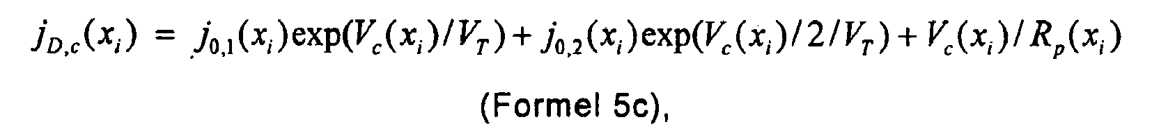
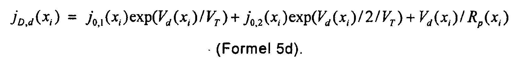
![]()
Insbesondere ist es vorteilhaft, in Schritt A zusätzlich eine weitere Messung, unter einer zu den Messbedingungen a, b und c unterschiedliche Messbedingungen d aufzuführen und in Schritt B entsprechend ein viertes Spannungsbild Vd(xi) zu bestimmen und die Dunkelstromdichte j D,a/b/c// d(xi) zusätzlich anhand einer weiteren Größe zu beschreiben. Entsprechend erfolgt in Schritt B die Bestimmung der ortsaufgelösten Eigenschaften der Halbleiterstruktur abhängig zumindest von den vier Spannungsbildern Va,b,c,d(xi). Hierbei wird vorzugsweise die Dunkelstromdichte zusätzlich durch eine zweite Diodenabhängigkeit gemäß des an sich bekannten Zweidiodenmodells mit einem zusätzlichen Diodenfaktor 2 beschrieben, bevorzugt gemäß Formeln 5a bis 5d: 

In einer weiteren vorzugsweisen Ausführungsform des erfindungsgemäßen Verfahrens werden die in Schritt B ermittelten Spannungsbilder dadurch von weiteren Messartdefekten befreit, dass die verschmierten Lumineszenzbilder durch Scharfzeichnungsfilter (beispielsweise Wienerfilter:
Zur Erhöhung der Genauigkeit der bestimmten Größen ist es vorteilhaft, dass in Schritt A mindestens eine weitere Messung unter einer weiteren, zu den Messbedingungen a und b unterschiedlichen Messbedingungen durchgeführt wird mindestens ein weiteres spannungskalibriertes Bild entsprechend bestimmt wird. In Schritt B liegt in dieser vorteilhaften Ausführungsform somit ein überbestimmtes gleiches System vor, welches in an sich bekannter Weise gelöst wird, vorzugsweise nach der Methode der kleinsten Quadrate. Hierdurch wird eine höhere Genauigkeit erzielt.In order to increase the accuracy of the specific variables, it is advantageous that in step A at least one further measurement is carried out under a further measurement condition different from the measurement conditions a and b, at least one further voltage-calibrated image is determined accordingly. In step B, in this advantageous embodiment, there is thus an over-determined, identical system which is released in a manner known per se, preferably according to the least-squares method. As a result, a higher accuracy is achieved.
Das Erzeugen und die Messung der Photolumineszenzstrahlung erfolgt vorzugsweise in an sich bekannter Weise und ist bispielsweise in
Insbesondere ist es vorteilhaft, bei dem erfindungsgemäßen Verfahren die Lumineszenzstrahlung mittels einer Kamera, wie beispielsweise einer CCD-Kamera zu messen. Das Messsignal der Kamera ist somit ein Maß für die Intensität der Lumineszenzstrahlung. Insbesondere kann durch Verwendung einer CCD-Kamera eine ortsaufgelöste Messung der Lumineszenzstrahlung direkt (durch ein so genanntes "Mapping") erfolgen, d. h. es ist kein Abrastern oder Scannen der Oberfläche der Halbleiterstruktur notwendig.In particular, it is advantageous in the method according to the invention to measure the luminescence radiation by means of a camera, such as a CCD camera. The measurement signal of the camera is thus a measure of the intensity of the luminescence radiation. In particular, by using a CCD camera, a spatially resolved measurement of the luminescence radiation can be carried out directly (by so-called "mapping"), ie. H. no scanning or scanning of the surface of the semiconductor structure is necessary.
Die Beaufschlagung der Oberfläche der Halbleiterstruktur zur Erzeugung der Photolumineszenzstrahlung erfolgt vorzugsweise mit homogener Intensität hinsichtlich der beaufschlagten Fläche der Halbleiterstruktur. Vorzugsweise wird die Halbleiterstruktur mit einem Normspektrum (beispielsweise das Spektrum AM1,5) beaufschlagt, ebenso liegt jedoch auch die Beaufschlagung mit anderen Spektren oder mit monochromatischer Anregungsstrahlung, beispielsweise durch Erzeugung mittels eines Lasers, im Rahmen der Erfindung. Ebenso ist es vorteilhaft, die Halbleiterstruktur mit unmoduliertem Licht als Anregungsstrahlung zu beaufschlagen.The application of the surface of the semiconductor structure for generating the photoluminescence radiation preferably takes place with a homogeneous intensity with regard to the applied surface of the semiconductor structure. Preferably, the semiconductor structure with a standard spectrum (for example, the spectrum AM 1.5) is applied, but also is the exposure to other Spectra or with monochromatic excitation radiation, for example by generation by means of a laser, within the scope of the invention. Likewise, it is advantageous to apply unmodulated light to the semiconductor structure as excitation radiation.
Weiterhin liegt es im Rahmen der Erfindung, dass die Beaufschlagung mit Anregungsstrahlung und die Messung der Lumineszenzstrahlung der Halbleiterstruktur an derselben Oberfläche der Halbleiterstruktur erfolgt. In diesem Fall ist es wesentlich, in an sich bekannter Weise bei der Messung der Lumineszenzstrahlung optische Filter vorzuschalten, um etwaige, an der Oberfläche der Halbleiterstruktur reflektierte Anregungsstrahlung herauszufiltern. Ebenso liegt es im Rahmen der Erfindung, die Beaufschlagung mit Anregungsstrahlung einerseits und die Messung der Lumineszenzstrahlung andererseits an zwei gegenüberliegenden Oberflächen der Halbleiterstruktur vorzunehmen. Bei dieser Messkonstellation wirkt die Halbleiterstruktur selbst als Filter gegenüber der Anregungsstrahlung, so dass bei dem Messvorgang keine Störeffekte aufgrund etwaiger detektierter Anregungsstrahlung auftreten.Furthermore, it is within the scope of the invention that the application of excitation radiation and the measurement of the luminescence radiation of the semiconductor structure take place on the same surface of the semiconductor structure. In this case, it is essential to preconnect optical filters in a manner known per se in the measurement of the luminescence radiation in order to filter out any excitation radiation reflected on the surface of the semiconductor structure. Likewise, it is within the scope of the invention to carry out the application of excitation radiation on the one hand and the measurement of the luminescence radiation on the other hand on two opposite surfaces of the semiconductor structure. In this measuring constellation, the semiconductor structure itself acts as a filter with respect to the excitation radiation, so that no disturbing effects due to any detected excitation radiation occur during the measuring process.
Die Messdaten der Lumineszenzstrahlung werden vorzugsweise durch eine Auswerteeinheit, wie beispielsweise einen Computer, ausgelesen und mittels diesem gemäß des erfindungsgemäßen Verfahrens weiter verarbeitet.The measurement data of the luminescence radiation are preferably read out by an evaluation unit, such as a computer, for example, and further processed by means of this according to the method according to the invention.
Sofern eine externe Spannung bei dem erfindungsgemäßen Messverfahren vorgegeben wird, wird diese vorzugsweise über eine steuerbare Spannungsquelle erzeugt, welche ebenfalls mit dem Computer zu deren Steuerung verbunden ist.If an external voltage is specified in the measuring method according to the invention, this is preferably generated via a controllable voltage source, which is also connected to the computer for their control.
Vorteilhafterweise umfasst die steuerbare Spannungsquelle zusätzlich eine Strommesseinheit, welche unter Kurzschlussbedingungen den fließenden Strom misst und das Messergebnis ebenfalls an den Computer weiterleitet. Auf diese Weise kann in einfacher Weise bei den jeweils vorliegenden Messbedingen die Kurzschlussstromdichte bestimmt werden.Advantageously, the controllable voltage source additionally comprises a current measuring unit, which measures the flowing current under short-circuit conditions and also forwards the measurement result to the computer. In this way, the short-circuit current density can be determined in a simple manner in each case present Meßbedingen.
Claims (15)
- A method of measuring a semiconductor structure, which includes an emitter and a base, and is solar cell or a precursor of a solar cell, including the following method steps:A producing luminescence radiation in the semiconductor structure and spatially resolved measurement of the luminescence radiation emanating from the semiconductor structure, wherein a first measurement is performed at a first measurement condition a and depending at least on the measurement data obtained in the first measurement a first spatially resolved, voltage-calibrated image Va(xi ) for a plurality of spatial points xi of the solar cell is determined from the measurement data obtained in step A,B determining spatially resolved properties of the semiconductor structure with regard to the spatially resolved dark saturation current jo(xi) and/or the spatially resolved emitter layer resistance ρ(xi) and/or the spatially resolved, local series resistance Rs(xi) for the plurality of spatial points xi dependent at least on the first voltage image Va(xi) determined in step A.
characterised in that,
in step A at least one second measurement is additionally performed at a second measurement condition b different to the first measurement condition a and dependent at least on the measurement data obtained from the second measurement a second spatially resolved, voltage-calibrated image Vb(xi) for the plurality of spatial points xi is determined from the measurement data obtained in step A,
that in both measurements in step A- the luminescence radiation is produced substantially by surface impingement of the semiconductor structure with an excitation radiation,- the measurement conditions (a, b) of the first and second measurements differ as regards the intensities and/or spectral compositions of the excitation radiation and/or a predetermined external voltage Vext which acts on the semiconductor structure via electrical contact,that additionally for each measurement condition (a, b) a voltage-independent, spatially independent short-circuit current density (jP,a, jP,b) of the current flowing under each of the measurement conditions when short-circuit conditions are present is predetermined and/or measured and that in step B the determination of the spatially resolved, electrical properties at each spatial point xi is effected in dependence on at least short-circuit current densities (jP,a, jP,b) and a voltage-dependent, spatially dependent dark current density (jD·a(xi), jD·b(xi)) for each measurement condition, wherein the dark current densities (jD·a(xi), jD·b(xi)) are dependent at least on the voltage-independent dark saturation current density jo(xi) and the two voltages (Va(xi), Vb(xi)) for the position xi resulting from the two voltage images. - A method as claimed in claim 1, characterised in that in step B the determination of the spatially resolved, electrical properties at each spatial point xi is effected additionally in dependence on external voltages Vext,a under a measurement condition a and Vext,b under measurement conditions b, wherein- in both measurements, in step A the semiconductor structure is electrically contacted and the external voltage Vext,a under measurement conditions a and the external voltage Vext,b under measurement condition b is predetermined via the electrical contact or- for the voltage Vext,a the voltage of the spatial point is predetermined with the lowest voltage in the voltage image Va(xi):

and correspondingly
- A method as claimed in claim 2,
characterised in that,
for each spatial point xi, in step B the determination of the spatially resolved electrical properties is effected such that a system of equations is solved, which for each of the two voltage images Va(xi) and Vb(xi) has a respective equation (Ga and Gb), wherein equation Ga comprises at least the spatially resolved, voltage-independent local series resistance Rs(xi), the voltage Va(xi), the short circuit current density jP,a and the dark current density jD,a(xi) and correspondingly Gb comprises at least Rs(xi), Vb(xi), Vext,b, jP,b and jD,b(xi) and that Rs(xi) and/or jo(xi) is determined by means of the equation system. - A method as claimed in claim 3, characterised in that the equation Ga has a structure in accordance with formula 1 a:

And Gb has a structure in accordance with formula 1 b:
- A method as claimed in at least one of claims 1 to 2, characterised in that for each spatial point xi in step B the determination of the spatially resolved, electrical properties is effected such that an equation system is solved, which has a respective equation (Ga' and Gb') for each of the two voltage images Va(xi) and Vb(xi) wherein equation Ga' comprises at least the spatially resolved, voltage-independent emitter layer resistance ρ(xi), the voltage Va(xi), the short circuit current density jP,a and the dark current density jD, a(xi) and correspondingly Gb' comprises at least ρ(xi ), Vb(xi), jP,b and jP,b(xi) and that ρ(xi) and/or jo(xi) is determined by means of the equation system.
- A method as claimed in claim 5, characterised in that the equation Ga' has structure in accordance with formula 2a:

and the equation Gb' has a structure in accordance with formula 2b
- A method as claimed in claim 6, characterised in that noise in the measurement data is reduced by the dual derivation in accordance with the Laplace-Operator in formulas 2a and 2b being replaced by the derivation of a polynomial, which is determined by means of a mathematical fit process or by using the Marr-Hildreth-Operator on the image.
- A method as claimed in one of claims 4 to 7, characterised in that additionally for each spatial point Xi and for each of the measurement conditions a and b an implicit open circuit voltage (Vimpl,a, Vimpl,b) is determined and the voltage calibrated images Va(xi) and Vb(xi ) are additionally determined with reference to the implicit open circuit voltages.
- A method as claimed in one at least claim 2, characterised in that in step A, under measurement condition a the illumination intensity and the spectrum of the excitation radiation is substantially the same as in measurement condition b, whereas under measurement condition a an external voltage Vext,a is predetermined, which is different to an external predetermined voltage Vext,b predetermined under measurement condition b.
- A method as claimed in at least one of the preceding claims, characterised in that the semiconductor structure is solar cell or a precursor of a solar cell and that in step A measurement condition a is so selected that a current in the range of 15% to 35%, preferably about 25%, of the short circuit current of the solar cell flows via the electrical contact under normal conditions and measurement condition b is so selected that a current in the range of 65% to 85% preferably about 75%, of the short circuit current of the solar cell under normal conditions flows via the electrical contact.
- A method as claimed in at least one of the preceding claims, characterised in that the dark current densities (jD,a(xi), jD, b(xi)) are described by means of a one diode model equation, particularly in accordance with formulas 3a and 3b:


- A method as claimed in at least one of the preceding claims, characterised in that in step A a further measurement is additionally performed under measurement condition c different to the measurement conditions a and b and a further voltage image Vc(xi) is determined, that the dark current densities are additionally described by way of a further parameter and in step B the determination of the spatially resolved properties of the semiconductor structure is effected in dependence on at least three voltage images, preferably, that the dark current densities are additionally described by a voltage-independent, local parallel resistance Rp(xi), preferably in accordance with formulas 4a to 4c:


- A method as claimed in claim 12, characterised in that in step A the further measurement is additionally performed under measurement condition d different to measurement conditions a, b and c and in step A a further voltage image Vd(xi) is determined, that the dark current densities are additionally described with reference to a further parameter and in step C the determination of the spatially resolved properties of the semiconductor structure is effected in dependence on at least the four voltage images, preferably, that the dark current density is additionally described by a second diode dependency with a diode factor of 2, preferably in accordance with the formulas 5a to 5d:


- A method as claimed in at least one of the preceding claims, characterised in that the voltage images determined in step A are freed of measurement noise and further measuring mode defects by the blurred luminescence images being corrected by sharpness filters, preferably by Wiener filters.
- A method as claimed in one of claims 3 or 5, characterised in that in step A at least one further measurement is performed under further measurement conditions different to measurement conditions a and b and at least one further voltage-calibrated image is determined and in step B an over determined equation system is solved, preferably by the least squares method.
Applications Claiming Priority (2)
| Application Number | Priority Date | Filing Date | Title |
|---|---|---|---|
| DE102009039399A DE102009039399A1 (en) | 2009-08-31 | 2009-08-31 | Method for measuring a semiconductor structure, which is a solar cell or a precursor of a solar cell |
| PCT/EP2010/005018 WO2011023312A1 (en) | 2009-08-31 | 2010-08-16 | Method for measuring a semiconductor structure, which is a solar cell or a precursor of a solar cell |
Publications (2)
| Publication Number | Publication Date |
|---|---|
| EP2473839A1 EP2473839A1 (en) | 2012-07-11 |
| EP2473839B1 true EP2473839B1 (en) | 2014-03-26 |
Family
ID=43128239
Family Applications (1)
| Application Number | Title | Priority Date | Filing Date |
|---|---|---|---|
| EP10744690.8A Active EP2473839B1 (en) | 2009-08-31 | 2010-08-16 | Method for measuring a semiconductor structure, which is a solar cell or a precursor of a solar cell |
Country Status (7)
| Country | Link |
|---|---|
| US (1) | US9435740B2 (en) |
| EP (1) | EP2473839B1 (en) |
| JP (1) | JP2013503354A (en) |
| CN (1) | CN102575987B (en) |
| AU (1) | AU2010288982A1 (en) |
| DE (1) | DE102009039399A1 (en) |
| WO (1) | WO2011023312A1 (en) |
Cited By (1)
| Publication number | Priority date | Publication date | Assignee | Title |
|---|---|---|---|---|
| DE102014208462A1 (en) * | 2014-05-06 | 2015-11-12 | Forschungszentrum Jülich GmbH | Method for measuring and evaluating power losses in solar cell, solar module and solar systems by means of photographic luminescence and thermography measurements |
Families Citing this family (15)
| Publication number | Priority date | Publication date | Assignee | Title |
|---|---|---|---|---|
| WO2012142651A1 (en) * | 2011-04-18 | 2012-10-26 | Bt Imaging Pty Ltd | Quantitative series resistance imaging of photovoltaic cells |
| US9246434B2 (en) | 2011-09-26 | 2016-01-26 | First Solar, Inc | System and method for estimating the short circuit current of a solar device |
| CN104412098B (en) | 2012-07-06 | 2018-10-30 | Bt成像股份有限公司 | The method for checking semiconductor wafer |
| US9880200B2 (en) * | 2013-09-04 | 2018-01-30 | Kla-Tencor Corporation | Method and apparatus for non-contact measurement of forward voltage, saturation current density, ideality factor and I-V curves in P-N junctions |
| US9823198B2 (en) * | 2013-09-14 | 2017-11-21 | Kla-Tencor Corporation | Method and apparatus for non-contact measurement of internal quantum efficiency in light emitting diode structures |
| FR3015770B1 (en) | 2013-12-19 | 2016-01-22 | Commissariat Energie Atomique | METHOD AND SYSTEM FOR QUALITY CONTROL OF PHOTOVOLTAIC CELLS |
| JP6280846B2 (en) * | 2014-09-09 | 2018-02-14 | 株式会社日立製作所 | Inspection method for solar cell module |
| TWI556570B (en) * | 2015-10-13 | 2016-11-01 | 財團法人工業技術研究院 | Measuring device for property of solar cell and measuring method using the same |
| US9866171B2 (en) | 2015-10-13 | 2018-01-09 | Industrial Technology Research Institute | Measuring device for property of photovoltaic device and measuring method using the same |
| DE102016119000B4 (en) * | 2016-10-06 | 2020-06-04 | Fraunhofer-Gesellschaft zur Förderung der angewandten Forschung e.V. | Calibration method and calibration device for a group of reflectors for concentrating solar radiation on a radiation receiver |
| CN107015087B (en) * | 2017-05-17 | 2019-04-26 | 华中科技大学 | A kind of capacitive property detection method of photoelectric device |
| FR3070560B1 (en) * | 2017-08-25 | 2019-09-13 | Electricite De France | METHOD FOR QUANTITATIVE ANALYSIS OF AN INSTALLATION COMPRISING A LIGHT EMITTING MODULE |
| CN108198907B (en) * | 2017-12-30 | 2020-02-11 | 苏州阿特斯阳光电力科技有限公司 | Silicon wafer determination method and device |
| CN113075172B (en) * | 2019-12-17 | 2023-01-03 | 苏州阿特斯阳光电力科技有限公司 | Method for testing composite current density distribution on surface of double-sided symmetrical passivated silicon wafer |
| CN115728273A (en) * | 2021-08-31 | 2023-03-03 | 环晟光伏(江苏)有限公司 | Method for representing solar cell metal recombination by using PL (PL) |
Family Cites Families (9)
| Publication number | Priority date | Publication date | Assignee | Title |
|---|---|---|---|---|
| US6541754B2 (en) * | 2000-07-05 | 2003-04-01 | Canon Kabushiki Kaisha | Method and apparatus for measuring photoelectric conversion characteristics of photoelectric conversion device |
| CN1216284C (en) * | 2003-01-07 | 2005-08-24 | 上海交通大学 | Test method for polycrystalline silicon solar battery converting efficiency |
| JP4861699B2 (en) | 2005-06-29 | 2012-01-25 | 株式会社コナミデジタルエンタテインメント | NETWORK GAME SYSTEM, NETWORK GAME SYSTEM CONTROL METHOD, GAME DEVICE, GAME DEVICE CONTROL METHOD, AND PROGRAM |
| DE102005040010A1 (en) * | 2005-08-23 | 2007-03-15 | Rwe Schott Solar Gmbh | Method and device for determining production errors in a semiconductor component |
| US8710860B2 (en) | 2006-05-05 | 2014-04-29 | Bt Imaging Pty Ltd | Method and system for testing indirect bandgap semiconductor devices using luminescence imaging |
| DE102007007140B4 (en) * | 2007-02-09 | 2009-01-29 | Astrium Gmbh | Method and arrangement for detecting mechanical defects of a semiconductor device, in particular a solar cell or solar cell arrangement |
| DE102007045830A1 (en) * | 2007-09-25 | 2009-04-02 | Kühn, Thomas | Solar cells i.e. solar panels, arrangement's defects localization and operability testing method for solar system, involves determining operability of arrangement and position of defective panel and/or cablings depending on camera image |
| JP5489107B2 (en) * | 2008-02-22 | 2014-05-14 | フラウンホーファー−ゲゼルシャフト ツール フエルデルング デア アンゲヴァンテン フォルシュング エー.ファオ. | Measuring method and apparatus for characteristic evaluation of semiconductor parts |
| EP2336752B1 (en) * | 2009-12-18 | 2018-12-05 | ISRA VISION Graphikon GmbH | Method and device for determining defective points in semiconductor components |
-
2009
- 2009-08-31 DE DE102009039399A patent/DE102009039399A1/en not_active Withdrawn
-
2010
- 2010-08-16 US US13/393,320 patent/US9435740B2/en active Active
- 2010-08-16 EP EP10744690.8A patent/EP2473839B1/en active Active
- 2010-08-16 AU AU2010288982A patent/AU2010288982A1/en not_active Abandoned
- 2010-08-16 JP JP2012527216A patent/JP2013503354A/en active Pending
- 2010-08-16 WO PCT/EP2010/005018 patent/WO2011023312A1/en active Application Filing
- 2010-08-16 CN CN201080035281.4A patent/CN102575987B/en active Active
Cited By (2)
| Publication number | Priority date | Publication date | Assignee | Title |
|---|---|---|---|---|
| DE102014208462A1 (en) * | 2014-05-06 | 2015-11-12 | Forschungszentrum Jülich GmbH | Method for measuring and evaluating power losses in solar cell, solar module and solar systems by means of photographic luminescence and thermography measurements |
| DE102014208462B4 (en) * | 2014-05-06 | 2016-04-14 | Forschungszentrum Jülich GmbH | Method for measuring and evaluating power losses in solar cell, solar module and solar systems by means of photographic luminescence and thermography measurements |
Also Published As
| Publication number | Publication date |
|---|---|
| DE102009039399A1 (en) | 2011-03-03 |
| CN102575987A (en) | 2012-07-11 |
| CN102575987B (en) | 2014-07-09 |
| US20120203494A1 (en) | 2012-08-09 |
| DE102009039399A8 (en) | 2011-06-01 |
| AU2010288982A1 (en) | 2012-02-09 |
| US9435740B2 (en) | 2016-09-06 |
| JP2013503354A (en) | 2013-01-31 |
| EP2473839A1 (en) | 2012-07-11 |
| WO2011023312A1 (en) | 2011-03-03 |
Similar Documents
| Publication | Publication Date | Title |
|---|---|---|
| EP2473839B1 (en) | Method for measuring a semiconductor structure, which is a solar cell or a precursor of a solar cell | |
| EP2245473B1 (en) | Measuring method and device for characterizing a semiconductor component | |
| DE19609521C2 (en) | Photo-induced current scanning analyzer capable of detecting photo-induced current in non-biased samples | |
| EP1624297B1 (en) | Weathering device comprising UV radiation sources and radiation sensors comprising a double-calibrated UV sensor | |
| DE102010061505B4 (en) | Method for inspection and detection of defects on surfaces of disc-shaped objects | |
| EP2433148B1 (en) | Method for spatially resolving series resistance of a semiconductor structure | |
| DE3116611C2 (en) | Device for measuring semiconductor properties | |
| DE3874469T2 (en) | MEASURING METHOD FOR SEMICONDUCTOR ARRANGEMENT. | |
| DE112018002123B4 (en) | METHOD OF DETERMINING A UNIFORMITY AND UNIFORMITY OF AN EFFECTIVE DOSE OF A LITHOGRAPHY TOOL AND SYSTEM FOR DETERMINING AN EFFECTIVE DOSE OF A LITHOGRAPHY TOOL | |
| EP0270578A1 (en) | Volume-measurement process for surface depressions | |
| DE68920187T2 (en) | Apparatus for measuring the peak voltage applied to a radiation source. | |
| EP2942634B1 (en) | Methods of measuring and evaluating power losses in solar cell, solar module, and solar facilities by means of photographic luminescence and thermography measurements | |
| DE10240060A1 (en) | Power loss measurement method for use in detecting local power loss distributions in optically sensitive semiconductors, e.g. solar cells, whereby components are illuminated with modulated radiation and thermographically imaged | |
| WO2010022922A1 (en) | Method for determining the excess charge carrier lifetime in a semiconductor layer | |
| DE10152679A1 (en) | Calibration of mass-produced CCD emission spectrometers, whereby calibration is split into spectrometer dependent and independent functions, with the independent function determined for all systems using a reference spectrometer | |
| EP0400373A2 (en) | Method for the spatial determination of the diffusion length of minority charge carriers in a semiconductive crystal body with the aid of an electrolytic cell | |
| EP2331942A1 (en) | Measuring method for a semiconductor structure | |
| EP0400386A2 (en) | Process for determining the recombination velocity of minority charges at the borders between semiconductors and other substances | |
| DE19915051C2 (en) | Method and device for the spatially resolved characterization of electronic properties of semiconductor materials | |
| DE102020114734B4 (en) | Method and device for in-situ determination of the temperature of a sample | |
| DE102015226708A1 (en) | Method and device for determining a measure of band gaps in optoelectronic devices | |
| EP2318851B1 (en) | Method for determining the recombination properties at a measuring section of a measuring side of a semiconductor structure | |
| DE2109590A1 (en) | Spectrometric measuring method and spectrometer arrangement for its implementation | |
| DE10248504A1 (en) | Non-destructive analysis process and use to determine condition of a solar cell uses raman spectra and electrical measurement of semiconductor layer before finishing cell | |
| EP2976651B1 (en) | Device for determining the charge carrier lifetime of a semiconductor substrate by measuring luminescent radiation and calibration method for calibrating such a device |
Legal Events
| Date | Code | Title | Description |
|---|---|---|---|
| PUAI | Public reference made under article 153(3) epc to a published international application that has entered the european phase |
Free format text: ORIGINAL CODE: 0009012 |
|
| 17P | Request for examination filed |
Effective date: 20120313 |
|
| AK | Designated contracting states |
Kind code of ref document: A1 Designated state(s): AL AT BE BG CH CY CZ DE DK EE ES FI FR GB GR HR HU IE IS IT LI LT LU LV MC MK MT NL NO PL PT RO SE SI SK SM TR |
|
| DAX | Request for extension of the european patent (deleted) | ||
| GRAJ | Information related to disapproval of communication of intention to grant by the applicant or resumption of examination proceedings by the epo deleted |
Free format text: ORIGINAL CODE: EPIDOSDIGR1 |
|
| GRAP | Despatch of communication of intention to grant a patent |
Free format text: ORIGINAL CODE: EPIDOSNIGR1 |
|
| GRAP | Despatch of communication of intention to grant a patent |
Free format text: ORIGINAL CODE: EPIDOSNIGR1 |
|
| RAP1 | Party data changed (applicant data changed or rights of an application transferred) |
Owner name: FRAUNHOFER-GESELLSCHAFT ZUR FOERDERUNG DER ANGEWAN Owner name: ALBERT-LUDWIGS-UNIVERSITAET FREIBURG |
|
| INTG | Intention to grant announced |
Effective date: 20131107 |
|
| GRAS | Grant fee paid |
Free format text: ORIGINAL CODE: EPIDOSNIGR3 |
|
| GRAA | (expected) grant |
Free format text: ORIGINAL CODE: 0009210 |
|
| AK | Designated contracting states |
Kind code of ref document: B1 Designated state(s): AL AT BE BG CH CY CZ DE DK EE ES FI FR GB GR HR HU IE IS IT LI LT LU LV MC MK MT NL NO PL PT RO SE SI SK SM TR |
|
| REG | Reference to a national code |
Ref country code: GB Ref legal event code: FG4D Free format text: NOT ENGLISH |
|
| REG | Reference to a national code |
Ref country code: CH Ref legal event code: EP |
|
| REG | Reference to a national code |
Ref country code: AT Ref legal event code: REF Ref document number: 659234 Country of ref document: AT Kind code of ref document: T Effective date: 20140415 |
|
| REG | Reference to a national code |
Ref country code: IE Ref legal event code: FG4D Free format text: LANGUAGE OF EP DOCUMENT: GERMAN |
|
| REG | Reference to a national code |
Ref country code: DE Ref legal event code: R096 Ref document number: 502010006490 Country of ref document: DE Effective date: 20140508 |
|
| PG25 | Lapsed in a contracting state [announced via postgrant information from national office to epo] |
Ref country code: NO Free format text: LAPSE BECAUSE OF FAILURE TO SUBMIT A TRANSLATION OF THE DESCRIPTION OR TO PAY THE FEE WITHIN THE PRESCRIBED TIME-LIMIT Effective date: 20140626 Ref country code: LT Free format text: LAPSE BECAUSE OF FAILURE TO SUBMIT A TRANSLATION OF THE DESCRIPTION OR TO PAY THE FEE WITHIN THE PRESCRIBED TIME-LIMIT Effective date: 20140326 |
|
| REG | Reference to a national code |
Ref country code: NL Ref legal event code: VDEP Effective date: 20140326 |
|
| REG | Reference to a national code |
Ref country code: LT Ref legal event code: MG4D |
|
| PG25 | Lapsed in a contracting state [announced via postgrant information from national office to epo] |
Ref country code: FI Free format text: LAPSE BECAUSE OF FAILURE TO SUBMIT A TRANSLATION OF THE DESCRIPTION OR TO PAY THE FEE WITHIN THE PRESCRIBED TIME-LIMIT Effective date: 20140326 Ref country code: SE Free format text: LAPSE BECAUSE OF FAILURE TO SUBMIT A TRANSLATION OF THE DESCRIPTION OR TO PAY THE FEE WITHIN THE PRESCRIBED TIME-LIMIT Effective date: 20140326 |
|
| PG25 | Lapsed in a contracting state [announced via postgrant information from national office to epo] |
Ref country code: LV Free format text: LAPSE BECAUSE OF FAILURE TO SUBMIT A TRANSLATION OF THE DESCRIPTION OR TO PAY THE FEE WITHIN THE PRESCRIBED TIME-LIMIT Effective date: 20140326 Ref country code: HR Free format text: LAPSE BECAUSE OF FAILURE TO SUBMIT A TRANSLATION OF THE DESCRIPTION OR TO PAY THE FEE WITHIN THE PRESCRIBED TIME-LIMIT Effective date: 20140326 |
|
| PG25 | Lapsed in a contracting state [announced via postgrant information from national office to epo] |
Ref country code: BG Free format text: LAPSE BECAUSE OF FAILURE TO SUBMIT A TRANSLATION OF THE DESCRIPTION OR TO PAY THE FEE WITHIN THE PRESCRIBED TIME-LIMIT Effective date: 20140626 Ref country code: RO Free format text: LAPSE BECAUSE OF FAILURE TO SUBMIT A TRANSLATION OF THE DESCRIPTION OR TO PAY THE FEE WITHIN THE PRESCRIBED TIME-LIMIT Effective date: 20140326 Ref country code: NL Free format text: LAPSE BECAUSE OF FAILURE TO SUBMIT A TRANSLATION OF THE DESCRIPTION OR TO PAY THE FEE WITHIN THE PRESCRIBED TIME-LIMIT Effective date: 20140326 Ref country code: EE Free format text: LAPSE BECAUSE OF FAILURE TO SUBMIT A TRANSLATION OF THE DESCRIPTION OR TO PAY THE FEE WITHIN THE PRESCRIBED TIME-LIMIT Effective date: 20140326 Ref country code: CY Free format text: LAPSE BECAUSE OF FAILURE TO SUBMIT A TRANSLATION OF THE DESCRIPTION OR TO PAY THE FEE WITHIN THE PRESCRIBED TIME-LIMIT Effective date: 20140326 Ref country code: CZ Free format text: LAPSE BECAUSE OF FAILURE TO SUBMIT A TRANSLATION OF THE DESCRIPTION OR TO PAY THE FEE WITHIN THE PRESCRIBED TIME-LIMIT Effective date: 20140326 Ref country code: IS Free format text: LAPSE BECAUSE OF FAILURE TO SUBMIT A TRANSLATION OF THE DESCRIPTION OR TO PAY THE FEE WITHIN THE PRESCRIBED TIME-LIMIT Effective date: 20140726 |
|
| PG25 | Lapsed in a contracting state [announced via postgrant information from national office to epo] |
Ref country code: PL Free format text: LAPSE BECAUSE OF FAILURE TO SUBMIT A TRANSLATION OF THE DESCRIPTION OR TO PAY THE FEE WITHIN THE PRESCRIBED TIME-LIMIT Effective date: 20140326 Ref country code: ES Free format text: LAPSE BECAUSE OF FAILURE TO SUBMIT A TRANSLATION OF THE DESCRIPTION OR TO PAY THE FEE WITHIN THE PRESCRIBED TIME-LIMIT Effective date: 20140326 Ref country code: SK Free format text: LAPSE BECAUSE OF FAILURE TO SUBMIT A TRANSLATION OF THE DESCRIPTION OR TO PAY THE FEE WITHIN THE PRESCRIBED TIME-LIMIT Effective date: 20140326 |
|
| REG | Reference to a national code |
Ref country code: HU Ref legal event code: AG4A Ref document number: E020732 Country of ref document: HU |
|
| PG25 | Lapsed in a contracting state [announced via postgrant information from national office to epo] |
Ref country code: PT Free format text: LAPSE BECAUSE OF FAILURE TO SUBMIT A TRANSLATION OF THE DESCRIPTION OR TO PAY THE FEE WITHIN THE PRESCRIBED TIME-LIMIT Effective date: 20140728 |
|
| REG | Reference to a national code |
Ref country code: DE Ref legal event code: R097 Ref document number: 502010006490 Country of ref document: DE |
|
| PG25 | Lapsed in a contracting state [announced via postgrant information from national office to epo] |
Ref country code: DK Free format text: LAPSE BECAUSE OF FAILURE TO SUBMIT A TRANSLATION OF THE DESCRIPTION OR TO PAY THE FEE WITHIN THE PRESCRIBED TIME-LIMIT Effective date: 20140326 |
|
| PLBE | No opposition filed within time limit |
Free format text: ORIGINAL CODE: 0009261 |
|
| STAA | Information on the status of an ep patent application or granted ep patent |
Free format text: STATUS: NO OPPOSITION FILED WITHIN TIME LIMIT |
|
| 26N | No opposition filed |
Effective date: 20150106 |
|
| PG25 | Lapsed in a contracting state [announced via postgrant information from national office to epo] |
Ref country code: LU Free format text: LAPSE BECAUSE OF FAILURE TO SUBMIT A TRANSLATION OF THE DESCRIPTION OR TO PAY THE FEE WITHIN THE PRESCRIBED TIME-LIMIT Effective date: 20140816 Ref country code: MC Free format text: LAPSE BECAUSE OF FAILURE TO SUBMIT A TRANSLATION OF THE DESCRIPTION OR TO PAY THE FEE WITHIN THE PRESCRIBED TIME-LIMIT Effective date: 20140326 Ref country code: IT Free format text: LAPSE BECAUSE OF FAILURE TO SUBMIT A TRANSLATION OF THE DESCRIPTION OR TO PAY THE FEE WITHIN THE PRESCRIBED TIME-LIMIT Effective date: 20140326 |
|
| REG | Reference to a national code |
Ref country code: DE Ref legal event code: R097 Ref document number: 502010006490 Country of ref document: DE Effective date: 20150106 |
|
| GBPC | Gb: european patent ceased through non-payment of renewal fee |
Effective date: 20140816 |
|
| PG25 | Lapsed in a contracting state [announced via postgrant information from national office to epo] |
Ref country code: BE Free format text: LAPSE BECAUSE OF NON-PAYMENT OF DUE FEES Effective date: 20140831 |
|
| REG | Reference to a national code |
Ref country code: IE Ref legal event code: MM4A |
|
| PG25 | Lapsed in a contracting state [announced via postgrant information from national office to epo] |
Ref country code: GB Free format text: LAPSE BECAUSE OF NON-PAYMENT OF DUE FEES Effective date: 20140816 Ref country code: SI Free format text: LAPSE BECAUSE OF FAILURE TO SUBMIT A TRANSLATION OF THE DESCRIPTION OR TO PAY THE FEE WITHIN THE PRESCRIBED TIME-LIMIT Effective date: 20140326 |
|
| PG25 | Lapsed in a contracting state [announced via postgrant information from national office to epo] |
Ref country code: IE Free format text: LAPSE BECAUSE OF NON-PAYMENT OF DUE FEES Effective date: 20140816 |
|
| PG25 | Lapsed in a contracting state [announced via postgrant information from national office to epo] |
Ref country code: SM Free format text: LAPSE BECAUSE OF FAILURE TO SUBMIT A TRANSLATION OF THE DESCRIPTION OR TO PAY THE FEE WITHIN THE PRESCRIBED TIME-LIMIT Effective date: 20140326 |
|
| PG25 | Lapsed in a contracting state [announced via postgrant information from national office to epo] |
Ref country code: GR Free format text: LAPSE BECAUSE OF FAILURE TO SUBMIT A TRANSLATION OF THE DESCRIPTION OR TO PAY THE FEE WITHIN THE PRESCRIBED TIME-LIMIT Effective date: 20140627 Ref country code: MT Free format text: LAPSE BECAUSE OF FAILURE TO SUBMIT A TRANSLATION OF THE DESCRIPTION OR TO PAY THE FEE WITHIN THE PRESCRIBED TIME-LIMIT Effective date: 20140326 |
|
| PG25 | Lapsed in a contracting state [announced via postgrant information from national office to epo] |
Ref country code: TR Free format text: LAPSE BECAUSE OF FAILURE TO SUBMIT A TRANSLATION OF THE DESCRIPTION OR TO PAY THE FEE WITHIN THE PRESCRIBED TIME-LIMIT Effective date: 20140326 |
|
| REG | Reference to a national code |
Ref country code: FR Ref legal event code: PLFP Year of fee payment: 7 |
|
| REG | Reference to a national code |
Ref country code: AT Ref legal event code: MM01 Ref document number: 659234 Country of ref document: AT Kind code of ref document: T Effective date: 20150816 |
|
| PG25 | Lapsed in a contracting state [announced via postgrant information from national office to epo] |
Ref country code: AT Free format text: LAPSE BECAUSE OF NON-PAYMENT OF DUE FEES Effective date: 20150816 |
|
| REG | Reference to a national code |
Ref country code: FR Ref legal event code: PLFP Year of fee payment: 8 |
|
| PG25 | Lapsed in a contracting state [announced via postgrant information from national office to epo] |
Ref country code: MK Free format text: LAPSE BECAUSE OF FAILURE TO SUBMIT A TRANSLATION OF THE DESCRIPTION OR TO PAY THE FEE WITHIN THE PRESCRIBED TIME-LIMIT Effective date: 20140326 |
|
| REG | Reference to a national code |
Ref country code: FR Ref legal event code: PLFP Year of fee payment: 9 |
|
| PG25 | Lapsed in a contracting state [announced via postgrant information from national office to epo] |
Ref country code: AL Free format text: LAPSE BECAUSE OF FAILURE TO SUBMIT A TRANSLATION OF THE DESCRIPTION OR TO PAY THE FEE WITHIN THE PRESCRIBED TIME-LIMIT Effective date: 20140326 |
|
| P01 | Opt-out of the competence of the unified patent court (upc) registered |
Effective date: 20230524 |
|
| PGFP | Annual fee paid to national office [announced via postgrant information from national office to epo] |
Ref country code: CH Payment date: 20230902 Year of fee payment: 14 |
|
| PGFP | Annual fee paid to national office [announced via postgrant information from national office to epo] |
Ref country code: HU Payment date: 20230811 Year of fee payment: 14 Ref country code: FR Payment date: 20230821 Year of fee payment: 14 Ref country code: DE Payment date: 20230822 Year of fee payment: 14 |