EP2472529A1 - Thermistor and method for producing same - Google Patents
Thermistor and method for producing same Download PDFInfo
- Publication number
- EP2472529A1 EP2472529A1 EP10811774A EP10811774A EP2472529A1 EP 2472529 A1 EP2472529 A1 EP 2472529A1 EP 10811774 A EP10811774 A EP 10811774A EP 10811774 A EP10811774 A EP 10811774A EP 2472529 A1 EP2472529 A1 EP 2472529A1
- Authority
- EP
- European Patent Office
- Prior art keywords
- thermistor
- thin film
- film layer
- base material
- metal base
- Prior art date
- Legal status (The legal status is an assumption and is not a legal conclusion. Google has not performed a legal analysis and makes no representation as to the accuracy of the status listed.)
- Granted
Links
Images



Classifications
-
- G—PHYSICS
- G01—MEASURING; TESTING
- G01K—MEASURING TEMPERATURE; MEASURING QUANTITY OF HEAT; THERMALLY-SENSITIVE ELEMENTS NOT OTHERWISE PROVIDED FOR
- G01K7/00—Measuring temperature based on the use of electric or magnetic elements directly sensitive to heat ; Power supply therefor, e.g. using thermoelectric elements
- G01K7/16—Measuring temperature based on the use of electric or magnetic elements directly sensitive to heat ; Power supply therefor, e.g. using thermoelectric elements using resistive elements
- G01K7/22—Measuring temperature based on the use of electric or magnetic elements directly sensitive to heat ; Power supply therefor, e.g. using thermoelectric elements using resistive elements the element being a non-linear resistance, e.g. thermistor
-
- H—ELECTRICITY
- H01—ELECTRIC ELEMENTS
- H01C—RESISTORS
- H01C17/00—Apparatus or processes specially adapted for manufacturing resistors
-
- H—ELECTRICITY
- H01—ELECTRIC ELEMENTS
- H01C—RESISTORS
- H01C1/00—Details
- H01C1/14—Terminals or tapping points specially adapted for resistors; Arrangements of terminals or tapping points on resistors
- H01C1/1413—Terminals or electrodes formed on resistive elements having negative temperature coefficient
-
- H—ELECTRICITY
- H01—ELECTRIC ELEMENTS
- H01C—RESISTORS
- H01C1/00—Details
- H01C1/14—Terminals or tapping points specially adapted for resistors; Arrangements of terminals or tapping points on resistors
- H01C1/142—Terminals or tapping points specially adapted for resistors; Arrangements of terminals or tapping points on resistors the terminals or tapping points being coated on the resistive element
-
- H—ELECTRICITY
- H01—ELECTRIC ELEMENTS
- H01C—RESISTORS
- H01C17/00—Apparatus or processes specially adapted for manufacturing resistors
- H01C17/06—Apparatus or processes specially adapted for manufacturing resistors adapted for coating resistive material on a base
- H01C17/065—Apparatus or processes specially adapted for manufacturing resistors adapted for coating resistive material on a base by thick film techniques, e.g. serigraphy
-
- H—ELECTRICITY
- H01—ELECTRIC ELEMENTS
- H01C—RESISTORS
- H01C17/00—Apparatus or processes specially adapted for manufacturing resistors
- H01C17/28—Apparatus or processes specially adapted for manufacturing resistors adapted for applying terminals
- H01C17/281—Apparatus or processes specially adapted for manufacturing resistors adapted for applying terminals by thick film techniques
-
- H—ELECTRICITY
- H01—ELECTRIC ELEMENTS
- H01C—RESISTORS
- H01C7/00—Non-adjustable resistors formed as one or more layers or coatings; Non-adjustable resistors made from powdered conducting material or powdered semi-conducting material with or without insulating material
- H01C7/008—Thermistors
-
- H—ELECTRICITY
- H01—ELECTRIC ELEMENTS
- H01C—RESISTORS
- H01C7/00—Non-adjustable resistors formed as one or more layers or coatings; Non-adjustable resistors made from powdered conducting material or powdered semi-conducting material with or without insulating material
- H01C7/04—Non-adjustable resistors formed as one or more layers or coatings; Non-adjustable resistors made from powdered conducting material or powdered semi-conducting material with or without insulating material having negative temperature coefficient
-
- Y—GENERAL TAGGING OF NEW TECHNOLOGICAL DEVELOPMENTS; GENERAL TAGGING OF CROSS-SECTIONAL TECHNOLOGIES SPANNING OVER SEVERAL SECTIONS OF THE IPC; TECHNICAL SUBJECTS COVERED BY FORMER USPC CROSS-REFERENCE ART COLLECTIONS [XRACs] AND DIGESTS
- Y10—TECHNICAL SUBJECTS COVERED BY FORMER USPC
- Y10T—TECHNICAL SUBJECTS COVERED BY FORMER US CLASSIFICATION
- Y10T29/00—Metal working
- Y10T29/49—Method of mechanical manufacture
- Y10T29/49002—Electrical device making
- Y10T29/49082—Resistor making
- Y10T29/49085—Thermally variable
Definitions
- the present invention relates to a thermistor and a method for manufacturing the same, and particularly relates to a thermistor in which a metal base material, a thermistor thin film layer, and an electrode are laminated and a method for manufacturing the same.
- the thermistor has a plate-like metal which also serves as an electrode, a themosensitive resistor film formed on one surface of the plate-like metal substrate, and an electrode film formed on the themosensitive resistor film.
- the thermistor has a structure in which the plate-like metal substrate is used as one electrode and the electrode film formed on the top layer is used as another electrode, there is no choice but to use wire bonding for electrical connection to the electrode film. Therefore, it has been impossible to mount the same on a minimal space.
- the thermistor when used as a temperature sensor of IC component mounted on a printed-circuit board, there is a 150 to 200 ⁇ m minute space between the printed-circuit board and the IC component, and it is preferable to mount the thermistor in the space.
- the mounting by wire bonding does not allow mounting on such a minimal space.
- the themosensitive resistor film (thermistor thin film) has formed by a gas phase method, such as sputtering, in the thermistor, which has caused problems of an increase in the cost and poor productivity. Furthermore, the thermistor has had problems that, when cracking or the like occurs in the metal substrate or the themosensitive resistor film, the resistance has fluctuated to change the characteristics as a temperature sensor.
- a thermistor which is a first aspect of the invention has a metal base material, a thermistor thin film layer formed on the metal base material, and a pair of split electrodes formed on the thermistor thin film layer.
- the pair of split electrodes can be soldered by reflow to lands of a printed-circuit board and mounting by wire bonding is not required. Therefore, the thermistor can be mounted even on a minimal space of 200 ⁇ m or lower.
- the thickness of the metal base material is 10 to 80 ⁇ m and the thickness of the thermistor thin film layer is 1 to 10 ⁇ m
- a reduction in the height can be achieved and also flexibility is imparted due to the fact that the thin film thermistor and the metal base material are integrated. Therefore, even when a stress is applied to a thermistor, cracking is hard to occur in a thermistor thin film layer portion. Even when there are irregularities, level differences, and the like in the mounting space, the thermistor described above can be mounted.
- a method for manufacturing a thermistor which is a second aspect of the invention is a method for manufacturing a thermistor having a metal base material, a thermistor thin film layer formed on the metal base material, and a pair of split electrodes formed on the thermistor thin film layer, and the method includes a process of applying a ceramic slurry onto a carrier film with a predetermined thickness to form a ceramic green sheet serving as the thermistor thin film layer, a process of applying a metal powder containing paste onto the ceramic green sheet with a predetermined thickness to form a metal base material sheet serving as the metal base material, a process of applying an electrode onto a of the ceramic green sheet facing the surface, on which the metal base material sheet is formed, with a predetermined thickness to form a split electrode pattern serving as the split electrodes, and a process of integrally firing the metal base material sheet, the ceramic green sheet, and the split electrode pattern.
- the thermistor thin film layer is formed by a solid phase method, the thermistor thin film layer can be manufactured at a lower cost than that of a case where the thermistor thin film layer is manufactured by a gas phase method and also since the metal base material, the thermistor thin film layer, and the split electrodes are integrally fired, the occurrence of cracking in the metal base material or the thermistor thin film layer can be suppressed as much as possible.
- a thermistor can be obtained in which a reduction in the height or mounting by reflow can be achieved and which can be mounted on a minimum space. Moreover, since the thermistor thin film layer is formed by a solid phase method, the thermistor thin film layer can be manufactured at a low cost and the occurrence of cracking can be suppressed as much as possible by integrally firing.
- an NTC thermistor 1 A which is a first example is constituted by a metal material 11, a thermistor thin film layer 15 formed on the metal base material 11, and a pair of split electrodes 21 and 22 formed on the thermistor thin film layer 15.
- the metal base material 11 is formed into a sheet shape from a metal powder paste.
- the thermistor thin film layer 15 is formed into a sheet shape from a ceramic slurry.
- the split electrodes 21 and 22 are obtained by forming an electrode material paste into a predetermined shape. These three substances are integrally fired. At least the metal base material 11 and the thermistor thin film layer 15 may be fired.
- the thickness of the metal base material 11 is about 10 to 80 ⁇ m.
- the thickness of the thermistor thin film layer 15 is about 1 to 10 ⁇ m.
- the thickness of the split electrodes 21 and 22 is about 0.1 to 10 ⁇ m.
- the thickness as the entire thermistor 1A is about 10 to 100 ⁇ m,
- the entire length size of the thermistor 1A is defined as L
- the entire width size thereof is defined as W
- the distance between the split electrodes 21 and 22 is defined as Lp
- the short side length, the dimension to the end surface of the thermistor 1A, the long side length, and the dimension to the side surface of the thermistor 1A of the split electrodes 21 and 22 are defined as L1, Lg, W1, and Wg, respectively.
- the height dimension of the metal base material 11 is defined as Tb and the thickness of the thermistor thin film layer 15 is defined as Tt.
- the thermistor thin film layer 15 various ceramic materials containing Mn, Ni, Fe, Ti, Co, Al, Zn, and the like in an arbitrary combination and in an appropriate amount can be used. In practice, oxides of the transition metal elements mentioned above are mixed for use. However, carbonates, hydroxides, and the like of the elements may be used as a starting material.
- the metal base material 11 and the split electrodes 21 and 22 simple substances of precious metals, such as Ag, Pd, Pt, and Au, base metals, such as Cu, Ni, Al, W, and Ti or alloys containing the same can be used.
- a doctor blade method As a method for forming the metal base maternal 11 or the thermistor thin film layer 15 into a sheet shape, a doctor blade method is common. However, screen printing, gravure printing, and an ink jet method may be used. The formation of the split electrodes 21 and 22 can be performed by printing methods, such as screen printing, a sputtering method, or a vapor deposition method, Materials and manufacturing processes are described in detail later.
- the split electrodes 21 and 22 serve as input/output terminals, and resistances R1 and R2 are formed by the thermistor thin film layer 15 and are electrically connected in series through the metal base material11. More specifically, the split electrodes 21 and 22 constitute a thermistor circuit through the resistances R1 and R2 formed by the thermistor thin film layer 15 in a direct contact state.
- an energization state forms a path passing the thermistor thin film layer 15 of portions contacting the split electrodes 21 and 22 and the metal base material 11 as indicated by the arrow in Fig. 3 .
- cracking is likely to occur in the central portion of the thermistor thin film layer 15.
- the portion where cracking occurs is not an energization path. Therefore, the electrical characteristics as the thermistor 1A are not affected.
- the NTC thermistor 1A having the above-described configuration is used for a temperature sensor of IC component mounted on a printed-circuit board, for example.
- the thermistor 1A is mounted by soldering the split electrodes 21 and 22 by reflow onto the lands of the printed-circuit board. Since the height of the thermistor 1A which is the first example is reduced to about 10 to 100 ⁇ m, the thermistor 1A can be mounted on an about 150 to 200 ⁇ m space formed between the printed-circuit board and the lC component. Due to the fact that the thermistor 1A is mounted on the space, the Thermistor 1A can immediately respond to an increase in heat of the IC component as a temperature sensor.
- the thin film thermistor and the metal base material are integrated, flexibility is imparted. Therefore, even when a stress is applied to the thermistor, cracking is hard to occur in the thermistor thin film layer portion. Even when there are irregularities, level difference, and the like in a mounting space, the thermistor 1A can be mounted.
- an Mn-Ni-Fe-Ti oxide was weighed in such a manner as to have a predetermined proportion (in such a manner that the resistivity is 104 ⁇ cm), sufficiently wet-grounded in a ball mill using a grinding medium, such as zirconia, and thereafter fired at a predetermined temperature, thereby obtaining ceramic powder.
- An organic binder was added to the ceramic powder, followed by wet mixing treatment to form a slurry. Then, the obtained slurry was formed into a ceramic green sheet, in which the thickness after firing was 1 to 15 ⁇ m, by a doctor blade method.
- a metal base material paste containing Ag-Pd as the main component was formed into a metal base material sheet, in which the thickness after firing was 5 to 100 ⁇ m, on the obtained ceramic green sheet by a doctor blade method.
- a 0.5 ⁇ m thick thermistor thin film layer was formed by a sputtering method on a 30 ⁇ m thick metal base material sheet to be used as a mother sheet for comparative examination.
- an Ag-Pd paste was screen-printed to thereby form split electrodes.
- each mother sheet on which the split electrodes were formed was cut into a I unit thermistor, accommodated in a zirconia sagger, subjected to debinding treatment, and then fired at a predetermined temperature (e.g., 900 to 1300°C).
- a predetermined temperature e.g., 900 to 1300°C.
- the ceramic slurry was applied onto a PET carrier film bye to thereby form the ceramic green sheet 15 serving as a thermistor thin film layer by a doctor blade method, and further the metal base material paste was applied thereon to thereby form the metal base material sheet 11 serving as a metal base material by a doctor blade method as illustrated in Fig. 4(A) .
- the film 31 and the sheets 15 and 11 are cut into a dimension for obtaining a multi-piece mother sheet ( Fig. 4(B) ), and the sheets 15 and 11 are separated from the film 31 ( Fig. 4(C) ).
- an Ag-Pd paste is screen-printed onto the sheet 15 to thereby form the split electrodes 21 and 22 ( Fig. 4(D) ), and then the sheet 15 is cut into a predetermined chip size ( fig. 4(E) ).
- the chip is fired to thereby obtain the laminated type thermistor 1A.
- the thermistors obtained in the above-described processes were subjected to various tests described below. Thereafter, the thermistors were observed under an optical microscope, a scanning electron microscope (SEM), and the like for the occurrence of defects (cracking).
- the room temperature resistance (which refers to the resistance at room temperature of 25°C, the same applies to the following description) was measured before and after the tests, and the occurrence of resistance change in the room temperature resistance by a load test was verified. With respect to the resistance change, it was judged that one in which the change ratio before and after performing the load test is lower than ⁇ 1% had no resistance change.
- thermistor test pieces having a length of 500 mm and a width of 5 mm were wound around cylinders having a diameter of 0.71 cm, 1.30 cm, 5.07 cm, and 10.13 cm equivalent to the curvature of then thermistors at a bending length of 1 mm, 2 mm, 8 mm, and 16 mm, and then held for 10 seconds.
- the thickness Tb of the metal base material was 30 ⁇ m and the thickness Tt of the thermistor thin film layer was 0.5 to 15.0 ⁇ m.
- the test results are as illustrated in Table 1.
- the evaluation was performer by observing cracking in the surface of the metal base material and measuring the resistance before and after the test.
- the occurrence oaf cracking was confirmed by observing the entire surface of the samples under an optical microscope with a magnification of 50 times and 100 times, and further observing the entire surface of the sample under a scanning electron microscope (SEM) with a magnification of 1000 times.
- SEM scanning electron microscope
- ⁇ represents that cracking was not observed and the resistance change ratio before and after the test was lower than ⁇ 1 %.
- ⁇ represents that cracking was observed but the resistance change ratio before and after the test was lower than ⁇ 1 %.
- ⁇ represents that cracking was observed and the resistance change ratio before and after the test was ⁇ 1 % or more.
- the thickness Tt of the thermistor thin film layer is larger than 10 ⁇ m, cracking occurs in a test in which the bending length is about 1 mm.
- the thickness is lower than 1 ⁇ m, the test results can be sufficiently appreciated but it is difficult to form a thermistor thin film layer whose thickness is lower than 1 ⁇ m by a solid phase method.
- a solid phase method is advantageous in terms of a manufacturing cost and productivity.
- the thickness Tt of the thermistor thin film layer is optimally 1.0 to 10 ⁇ m.
- the thermistor has flexibility which allows the thermistor to be wound around a cylinder having a diameter of 10.13 cm. More preferably, when the thickness Tt of the thermistor thin film layer is 2 ⁇ m or lower, the thermistor has excellent flexibility which allows the thermistor to be wound aground a cylinder having a diameter of 0.71 cm.
- thermistor test pieces having a length of 50 mm and a width of 5 mm were set in a tensile testing machine (Shimazu Autograph), and the load in cutting was measured.
- the width dimension W of the metal base material was 500 ⁇ m
- the thickness Tb thereof was 5 to 100 ⁇ m
- the thickness Tt of the thermistor thin film layer was 3 ⁇ m.
- the thickness Tb of the metal base material is smaller thin 10 ⁇ m, the tensile strength is remarkably low. For example, when mounted on a printed-circuit board, there is a possibility that the thermistor may be broken due to a solder stress between lands. Moreover, the handling in terms of manufacturing is difficult.
- the thickness Tb is larger than 80 ⁇ m, the tensile strength is enough but the used amount of the metal materials increases to increase the cost and a reduction in the height of the thermistor is impaired, Therefore, the thickness Tb of the metal base material is preferably 10 to 80 ⁇ m.
- the upper limit of the thickness Tab is not necessarily limited in terms of strength.
- Metal base material width ( ⁇ m) Metal base material thickness Tb ( ⁇ m) Thermistor thin film layer thickness Tt ( ⁇ m) Fracture strength (kgf) 500 5 3.0 3.8 500 10 3.0 7.6 500 30 3.0 22.6 500 50 3.0 37.6 500 80 3.0 60.1 500 100 3.0 75.1
- the resistance at room temperature (25°C) at the distance Lp between the split electrodes was calculated by simulation using FEM (finite element method).
- the applied voltage in this case was 1 V.
- the resistance change ratio AR/R (%/ ⁇ m) from the room temperature resistance R in accordance with the change in the distance Lp when the distance Lp between the split electrodes was 2.0 to 200 ⁇ m and the thickness Tt of the thermistor thin film layer was changed in the range of 1.0 to 10.0 ⁇ m (k ⁇ ) was calculated by the following equation. When the value is larger, the variation in the resistance value is larger.
- Lp1 and Lp2 are continuous and adjacent numerical values in the table and Lp1 > Lp2 is established.
- Lp1 is 200 ⁇ m
- Lp2 is 190 ⁇ m
- Lp1 is 190 ⁇ m
- Lp2 is 180 ⁇ m.
- a comparison target does not exist in the case of the lowest column of the table (Lp is 2.0 ⁇ m in Table 3)
- - is indicated.
- ⁇ R/R %/ ⁇ m
- ⁇ R/R (%/ ⁇ m) becomes larger than 1.00 even when the values of Lp1 and Lp2 are made smaller than the value. Therefore, the experiment is omitted and - is indicated.
- the resistance change ratio ⁇ R/R is lower than ⁇ 0.2%. More specifically, the distance Lp is preferably Tt + 5 ⁇ m or more. When the distance is smaller than Tt + 5 ⁇ m, the element resistance is not only in the thickness direction but in the surface direction. As a result, the contribution to the resistance of the distance Lp becomes large, and the resistance value varies due to processing error, Moreover, when cracking or the like occurs between the split electrodes, the resistance value changes.
- the end surface distance Lg of the split electrodes was also determined by simulation for the resistance at room temperature (25°C).
- the results of calculating the room temperature resistance R (k ⁇ ) and the resistance change ratio ⁇ R/R (%/ ⁇ m) when the end surface distance Lg was 0.0 to 20.0 ⁇ m and the thickness Tt of the thermistor thin film layer was changed in the range of 1.0 to 10.0 ⁇ m are shown in Table 4.
- the side surface distance Wg is 20 ⁇ m and other numerical values are indicated in the margin of Table 4.
- the side surface distance Wg of the split electrode resistances was also determined by simulation for the resistance value.
- the results of calculating the room temperature resistance R (k ⁇ ) and the resistance change ratio ⁇ R/R (%/ ⁇ m) when the side surface distance Wg was 0.0 to 20.0 ⁇ m and the thickness Tt of the thermistor thin film layer was changed in the range of 1.0 to 10.0 ⁇ m are shown in Table 5.
- the end surface distance Lg is 20 ⁇ m and other numerical values are indicated in the margin of Table 5.
- the resistance change ratio ⁇ R/R is lower than ⁇ 0.2% also about the distance Lg and the distance Wg. More specifically, it is preferable to secure the distance Lg and the distance Wg to be 5 ⁇ m or more, and the influence of the resistance change resulting from the surface at the end surface and the side surface can be prevented.
- the coefficient of linear expansion shown in Tables 6 and 7 are the results of manufacturing a square column having a cross section of 2.0 mm ⁇ 2.0 mm and a length of 5.0 mm from a material of the metal base material and a material of the thermistor thin film, and measuring the coefficient of linear expansion by TEA in the air atmosphere.
- the value of the coefficient of linear expansion at 800°C is indicated on the basis of 30°C. With respect to the measurement conditions, the temperature elevation was 10°C/min and a load was 10 gf.
- an NTC thermistor 1B which is a third example has the metal base material 11, the thermistor thin film layer 15, and the split electrodes 21 and 22 as illustrated in Fig. 5 , and, in addition, a protection layer 16 is formed on the thermistor thin film layer 15 and an Ni plating layer 23 and an Sn plating layer 24 are formed on the split electrodes 21 and 22.
- Ni plating layer 23' and an Sn plating layer 24' are formed also on the surface of the metal base material 11. However, the layers are formed simultaneously with the formation of the plating layers 23 and 24. By these plating layers 23' and 24', an effect of preventing the migration of Ag can be expected when the metal base material 11 is Ag/Pd or the like,
- the protection layer 16 is one which suppresses the corrosion of the thermistor thin film layer 15 by plating in the formation of the plating layers 23 and 24 and which may be an insulator material, such as glass, resin, or insulator ceramic, which is not corroded by plating.
- insulator ceramic is used as the protection layer 16 by forming an insulator ceramic green sheet on the thermistor thin film layer 15 beforehand when integrally firing the metal base material 11 and the thermistor thin film layer 15, the metal base material 11, the thermistor thin film layer 15, and the protection layer 16 can be formed by integrally firing, so that the manufacturing process is simplified and the adhesion of the thermistors thin film layer 15 and the protection layer 16 becomes good.
- a thermistor 1B' illustrated in Fig. 6 is one in which a protection layer 16 is formed also of the back surface or the side surfaces of the metal base material 11, as compared with the thermistor 1B illustrated in Fig. 5 .
- This kind of the thermistor is mounted by reflow on lands 41 formed on the surface of a printed-circuit board 40 through solders 42.
- conductive parts, wiring, and the like which are not illustrated may be electrically conductive to the metal base material 11.
- a thermistor 1C which is a fourth example is one in which the thermistor thin film layers 15 are formed immediately under the split electrodes 21 and 22 in a rectangular shape slightly smaller than the split electrodes 21 and 22 as illustrated in Fig. 7 .
- the configuration such that the Ni plating layer 23 and the Sn plating layer 24 are formed on the split electrode 21 and 22 is the same as in the third example.
- the firing condition and the sintering behavior of the protection layer 16 changes in the A section due to a difference of the foundation, which results in a possibility that cracking may occur in the A section.
- the entire foundation of the protection layer 16 is the metal base material 11, so that the presence of the A section which is an overlapped portion is canceled. Therefore, there is no possibility of the occurrence of cracking also disappears and the total thickness as a thermistor becomes small.
- the results of measuring samples No. 1 to No. 4 shown in Table 9 for the resistance value change resuming from the variation in the area of the split electrodes 21 and 22 are shown.
- the area (L1 ⁇ W1) of the split electrodes 21 and 22 was set to 310 ⁇ m square, 300 ⁇ m square, and 290 ⁇ m square (three types), the resistivity p1 of the thermistor material ways 10 k ⁇ cm, and the resistivity p2 of the protection layer 16 was set 10 k ⁇ cm in the sample No. 1, 100 k ⁇ cm in the sample No. 2, 1000 k ⁇ cm in the sample No.
- the area of the thermistor thin film layer 15 is 250 ⁇ 250 ⁇ m and the thickness (Tt) is 3 ⁇ m.
- L was 1000 ⁇ m
- W was 500 ⁇ m
- Tb was 30 ⁇ m
- Lg was 20 ⁇ m
- Lp was 960 ⁇ m - L direction dimension of the split electrodes (290, 300, or 310 ⁇ m)
- Wig was 20 ⁇ m.
- ⁇ 1 represents the resistivity of a thermistor material (specifically, Mn-Ni-Fe-Ti thermistor material) formed into the thermistor thin film layer.
- ⁇ 2 represents the resistivity of an insulator material (specifically, Fe-Mn ferrite material) formed into the protection layer. The resistivity is changed by changing the composition ratio.
- the resistance value change (%) was calculated by the following equation.
- Resistance value change R ⁇ 2 - R ⁇ 1 / R ⁇ 1 ⁇ 100
- the resistance value change (%) was 14.27 when ⁇ 2/ ⁇ 1 was 1 (Sample No. 1), 1.86 when ⁇ 2/ ⁇ 1 was 10 (Sample No, 2), 0.19 when ⁇ 2/ ⁇ 1 was 100 (Sample No. 3), and 0.02 when ⁇ 2/ ⁇ 1 was 1000 (Sample No. 4).
- ⁇ 2/ ⁇ 1 is 100 times or more, the resistance value change can be suppressed to 0.2% or lower even when the area of the split electrodes 21 and 22 varies. Therefore, the ⁇ 2/ ⁇ 1 ratio is preferable.
- a thermistor 1D which is a fifth example is one in which the area of the thermistor thin film layers 15 is made larger than the area of the split electrodes 21 and 22 as illustrated in Fig. 8 .
- peripheral portions B of the thermistor thin film layers 15 were located outside to the peripheral portion of the split electrodes 21 and 22 and the protection layer 16 covers a region from the peripheral portions B to a part of the inner side of the thermistor thin film layer 15.
- the other configurations are the same as those of the fourth example.
- the protection layer 16 covers the peripheral portions B of the thermistor thin film layers 15. Therefore, by bringing the protection layer 16 into close contact with the metal base material 11, the thermistor thin film layers 15 are held, so that the thermistor thin film layers 15 are prevented from separating from the metal base material 11. Supposing that the thermistor thin film layers 15 are separated from the metal base material 11, the area to which the resistance value contributes decreases, so that the resistance value tends to increase.
- the invention is free from the problem. Since the protection layer 16 does not contribute to the thermistor characteristics, a material having high adhesion with the metal base material 11 may be selected.
- the protection layer 16 was formed in such a manner that a part thereof is overlapped with the peripheral portions of the thermistor thin film layers 15, and then the split electrodes 21 and 22 were formed, peripheral portions of the protection layer 16 are formed between the peripheral portions at the side of the thermistor thin film layer 15 of the split electrodes 21 and 22 and the thermistor thin film layer 15.
- the thermistor and the method for manufacturing the same according to the invention are not limited to the Examples above, and can be modified in various manners within the scope thereof.
- thermistor shown in the Examples above are merely examples.
- shape and the like of the details of the metal base material, the thermistor thin film layer, and the split electrodes are arbitrary.
- the invention is useful for a thermistor and a method for manufacturing the same and particularly is excellent in that a reduction in the height or mounting by reflow or the like can be achieved, the thermistor can be manufactured at a low cost, and the occurrence of cracking can be suppressed as much as possible.
Landscapes
- Engineering & Computer Science (AREA)
- Microelectronics & Electronic Packaging (AREA)
- Physics & Mathematics (AREA)
- Manufacturing & Machinery (AREA)
- Electromagnetism (AREA)
- Nonlinear Science (AREA)
- General Physics & Mathematics (AREA)
- Thermistors And Varistors (AREA)
- Apparatuses And Processes For Manufacturing Resistors (AREA)
Abstract
Description
- The present invention relates to a thermistor and a method for manufacturing the same, and particularly relates to a thermistor in which a metal base material, a thermistor thin film layer, and an electrode are laminated and a method for manufacturing the same.
- As an ETC thermistor or a PTC thermistor used as a temperature sensor or the like in a protection circuit heretofore, one disclosed in
Patent Document 1 is known. The thermistor has a plate-like metal which also serves as an electrode, a themosensitive resistor film formed on one surface of the plate-like metal substrate, and an electrode film formed on the themosensitive resistor film. - However, since the thermistor has a structure in which the plate-like metal substrate is used as one electrode and the electrode film formed on the top layer is used as another electrode, there is no choice but to use wire bonding for electrical connection to the electrode film. Therefore, it has been impossible to mount the same on a minimal space. For example, when used as a temperature sensor of IC component mounted on a printed-circuit board, there is a 150 to 200 µm minute space between the printed-circuit board and the IC component, and it is preferable to mount the thermistor in the space. However, the mounting by wire bonding does not allow mounting on such a minimal space.
- Moreover, the themosensitive resistor film (thermistor thin film) has formed by a gas phase method, such as sputtering, in the thermistor, which has caused problems of an increase in the cost and poor productivity. Furthermore, the thermistor has had problems that, when cracking or the like occurs in the metal substrate or the themosensitive resistor film, the resistance has fluctuated to change the characteristics as a temperature sensor.
-
- PAL 1: Japanese Unexamined Patent Application Publication No.
61-245502 - It is an object of the present invention to provide a thermistor which can be mounted by reflow and can be mounted on a minimal space and a method for manufacturing the same. It is another object of the invention to provide a thermistor in which a reduction in the height can be achieved and the occurrence of cracking can be suppressed as much as possible and which can be manufactured at a low cost and a method for manufacturing the same.
- A thermistor which is a first aspect of the invention has a metal base material, a thermistor thin film layer formed on the metal base material, and a pair of split electrodes formed on the thermistor thin film layer.
- In the thermistor, the pair of split electrodes can be soldered by reflow to lands of a printed-circuit board and mounting by wire bonding is not required. Therefore, the thermistor can be mounted even on a minimal space of 200 µm or lower.
- In particular, when the thickness of the metal base material is 10 to 80 µm and the thickness of the thermistor thin film layer is 1 to 10 µm, a reduction in the height can be achieved and also flexibility is imparted due to the fact that the thin film thermistor and the metal base material are integrated. Therefore, even when a stress is applied to a thermistor, cracking is hard to occur in a thermistor thin film layer portion. Even when there are irregularities, level differences, and the like in the mounting space, the thermistor described above can be mounted.
- Moreover, even when an excessive stress is applied to the thermistor to cause bending, so that cracking occurs in the central part of the thermistor thin film layer, the electrical characteristics as the thermistor are hard to be affected the thermistor employs split electrodes and the central portion of the thermistor thin film layer is not an energizing path.
- A method for manufacturing a thermistor which is a second aspect of the invention is a method for manufacturing a thermistor having a metal base material, a thermistor thin film layer formed on the metal base material, and a pair of split electrodes formed on the thermistor thin film layer, and the method includes a process of applying a ceramic slurry onto a carrier film with a predetermined thickness to form a ceramic green sheet serving as the thermistor thin film layer, a process of applying a metal powder containing paste onto the ceramic green sheet with a predetermined thickness to form a metal base material sheet serving as the metal base material, a process of applying an electrode onto a of the ceramic green sheet facing the surface, on which the metal base material sheet is formed, with a predetermined thickness to form a split electrode pattern serving as the split electrodes, and a process of integrally firing the metal base material sheet, the ceramic green sheet, and the split electrode pattern.
- In the manufacturing method, since the thermistor thin film layer is formed by a solid phase method, the thermistor thin film layer can be manufactured at a lower cost than that of a case where the thermistor thin film layer is manufactured by a gas phase method and also since the metal base material, the thermistor thin film layer, and the split electrodes are integrally fired, the occurrence of cracking in the metal base material or the thermistor thin film layer can be suppressed as much as possible.
- According to the present invention, a thermistor can be obtained in which a reduction in the height or mounting by reflow can be achieved and which can be mounted on a minimum space. Moreover, since the thermistor thin film layer is formed by a solid phase method, the thermistor thin film layer can be manufactured at a low cost and the occurrence of cracking can be suppressed as much as possible by integrally firing.
-
- [
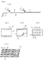
Fig. 1] fig. 1 illustrates a thermistor which is a first example, in whichFig. 1(A) is a plan view andFig. 1(B) is a front view. - [
Fig. 2] Fig. 2 is an equivalent circuit diagram of the thermistor. - [
Fig. 3] Fig. 3 is an explanatory view for illustrating the energization state of the thermistor. - [
Fig. 4] Fig. 4 is explanatory view for illustrating manufacturing processes of the thermistor. - [
Fig. 5] Fig. 5 is a cross sectional view illustrating a thermistor which is a third example. - [
Fig. 6] Fig. 6 is a cross sectional view illustrating a modification of the thermistor which is the third example. - [
Fig. 7] Fig. 7 is a cross sectional view illustrating a thermistor which is a fourth example. - [
Fig. 8] Fig. 8 is a cross sectional view illustrating a thermistor which is a fifth example, - Hereinafter, Examples of a thermistor and a method for manufacturing the same according to the invention are described with reference to the attached drawings. In each drawing, common parts and common portions are designated by the same reference numerals, and the same explanation is omitted.
- As illustrated in Fug. 1, an
NTC thermistor 1 A which is a first example is constituted by ametal material 11, a thermistorthin film layer 15 formed on themetal base material 11, and a pair ofsplit electrodes thin film layer 15. Themetal base material 11 is formed into a sheet shape from a metal powder paste. The thermistorthin film layer 15 is formed into a sheet shape from a ceramic slurry. Thesplit electrodes metal base material 11 and the thermistorthin film layer 15 may be fired. - The thickness of the
metal base material 11 is about 10 to 80 µm. The thickness of the thermistorthin film layer 15 is about 1 to 10 µm. The thickness of thesplit electrodes entire thermistor 1A is about 10 to 100 µm, Herein, the entire length size of thethermistor 1A is defined as L, the entire width size thereof is defined as W, the distance between thesplit electrodes thermistor 1A, the long side length, and the dimension to the side surface of thethermistor 1A of thesplit electrodes metal base material 11 is defined as Tb and the thickness of the thermistorthin film layer 15 is defined as Tt. - As the thermistor
thin film layer 15, various ceramic materials containing Mn, Ni, Fe, Ti, Co, Al, Zn, and the like in an arbitrary combination and in an appropriate amount can be used. In practice, oxides of the transition metal elements mentioned above are mixed for use. However, carbonates, hydroxides, and the like of the elements may be used as a starting material. As themetal base material 11 and thesplit electrodes - As a method for forming the metal base maternal 11 or the thermistor
thin film layer 15 into a sheet shape, a doctor blade method is common. However, screen printing, gravure printing, and an ink jet method may be used. The formation of thesplit electrodes - Here, an equivalent circuit of the
thermistor 1A is described with reference toFig. 2 . Thesplit electrodes thin film layer 15 and are electrically connected in series through the metal base material11. More specifically, thesplit electrodes thin film layer 15 in a direct contact state. - Since the
split electrodes thin film layer 15, an energization state forms a path passing the thermistorthin film layer 15 of portions contacting thesplit electrodes metal base material 11 as indicated by the arrow inFig. 3 . In bending or mounting with a mounter of thethermistor 1A, cracking is likely to occur in the central portion of the thermistorthin film layer 15. However, even when cracking occurs in the central portion of the thermistorthin film layer 15, the portion where cracking occurs is not an energization path. Therefore, the electrical characteristics as thethermistor 1A are not affected. - The
NTC thermistor 1A having the above-described configuration is used for a temperature sensor of IC component mounted on a printed-circuit board, for example. In this case, thethermistor 1A is mounted by soldering thesplit electrodes thermistor 1A which is the first example is reduced to about 10 to 100 µm, thethermistor 1A can be mounted on an about 150 to 200 µm space formed between the printed-circuit board and the lC component. Due to the fact that thethermistor 1A is mounted on the space, theThermistor 1A can immediately respond to an increase in heat of the IC component as a temperature sensor. - Moreover, due to the fact that the thin film thermistor and the metal base material are integrated, flexibility is imparted. Therefore, even when a stress is applied to the thermistor, cracking is hard to occur in the thermistor thin film layer portion. Even when there are irregularities, level difference, and the like in a mounting space, the
thermistor 1A can be mounted. - Next, a manufacturing process of the
thermistor 1A is described. First, as a raw material of the thermistorthin film layer 15, an Mn-Ni-Fe-Ti oxide was weighed in such a manner as to have a predetermined proportion (in such a manner that the resistivity is 104 Ωcm), sufficiently wet-grounded in a ball mill using a grinding medium, such as zirconia, and thereafter fired at a predetermined temperature, thereby obtaining ceramic powder. - An organic binder was added to the ceramic powder, followed by wet mixing treatment to form a slurry. Then, the obtained slurry was formed into a ceramic green sheet, in which the thickness after firing was 1 to 15 µm, by a doctor blade method. A metal base material paste containing Ag-Pd as the main component was formed into a metal base material sheet, in which the thickness after firing was 5 to 100 µm, on the obtained ceramic green sheet by a doctor blade method. Furthermore, for comparative examination, a 0.5 µm thick thermistor thin film layer was formed by a sputtering method on a 30 µm thick metal base material sheet to be used as a mother sheet for comparative examination. Hereafter, on the ceramic green sheet, an Ag-Pd paste was screen-printed to thereby form split electrodes.
- Next, each mother sheet on which the split electrodes were formed was cut into a I unit thermistor, accommodated in a zirconia sagger, subjected to debinding treatment, and then fired at a predetermined temperature (e.g., 900 to 1300°C). Thus, the
thermistor 1A of a laminated type having themetal base material 11, the thermistorthin film layer 15, and thesplit electrodes - As specific processes, the ceramic slurry was applied onto a PET carrier film bye to thereby form the ceramic
green sheet 15 serving as a thermistor thin film layer by a doctor blade method, and further the metal base material paste was applied thereon to thereby form the metalbase material sheet 11 serving as a metal base material by a doctor blade method as illustrated inFig. 4(A) . Thefilm 31 and thesheets Fig. 4(B) ), and thesheets Fig. 4(C) ). Thereafter, an Ag-Pd paste is screen-printed onto thesheet 15 to thereby form thesplit electrodes 21 and 22 (Fig. 4(D) ), and then thesheet 15 is cut into a predetermined chip size (fig. 4(E) ). The chip is fired to thereby obtain thelaminated type thermistor 1A. - The thermistors obtained in the above-described processes were subjected to various tests described below. Thereafter, the thermistors were observed under an optical microscope, a scanning electron microscope (SEM), and the like for the occurrence of defects (cracking). The room temperature resistance (which refers to the resistance at room temperature of 25°C, the same applies to the following description) was measured before and after the tests, and the occurrence of resistance change in the room temperature resistance by a load test was verified. With respect to the resistance change, it was judged that one in which the change ratio before and after performing the load test is lower than ±1% had no resistance change.
- First, a winding test was carried out. In the winding test, thermistor test pieces having a length of 500 mm and a width of 5 mm were wound around cylinders having a diameter of 0.71 cm, 1.30 cm, 5.07 cm, and 10.13 cm equivalent to the curvature of then thermistors at a bending length of 1 mm, 2 mm, 8 mm, and 16 mm, and then held for 10 seconds. In the test pieces, the thickness Tb of the metal base material was 30 µm and the thickness Tt of the thermistor thin film layer was 0.5 to 15.0 µm.
- The test results are as illustrated in Table 1. The evaluation was performer by observing cracking in the surface of the metal base material and measuring the resistance before and after the test. The occurrence oaf cracking was confirmed by observing the entire surface of the samples under an optical microscope with a magnification of 50 times and 100 times, and further observing the entire surface of the sample under a scanning electron microscope (SEM) with a magnification of 1000 times. In the evaluation column of Table 1, ⊙ represents that cracking was not observed and the resistance change ratio before and after the test was lower than ±1 %. ○ represents that cracking was observed but the resistance change ratio before and after the test was lower than ±1 %. × represents that cracking was observed and the resistance change ratio before and after the test was ±1 % or more.
-
[Table 1] Metal base material thickness Tb (µm) Thermistor thin film layer thickness Tt (µm) Diameter of cylinders in winding test (cm) 0.71 1.30 5.07 10.13 30 0.5 ⊙ ⊙ ⊙ ⊙ 30 1.0 ⊙ ⊙ ⊙ ⊙ 30 2.0 ⊙ ⊙ ⊙ ⊙ 30 3.0 ○ ⊙ ⊙ ⊙ 30 5.0 × ○ ⊙ ⊙ 30 10.0 × × ○ ⊙ 30 15.0 × × × × - According to the winding test described above, when the thickness Tt of the thermistor thin film layer is larger than 10 µm, cracking occurs in a test in which the bending length is about 1 mm. When the thickness is lower than 1 µm, the test results can be sufficiently appreciated but it is difficult to form a thermistor thin film layer whose thickness is lower than 1 µm by a solid phase method. A solid phase method is advantageous in terms of a manufacturing cost and productivity. When supposing that a solid phase method is used, the thickness Tt of the thermistor thin film layer is optimally 1.0 to 10 µm.
- Thus, by integrating the thin film thermistor and the metal base material, flexibility is imparted to the thermistor. It has been found that, in particular, when the thickness Tt of the thermistor thin film layer is 10 µm or lower, the thermistor has flexibility which allows the thermistor to be wound around a cylinder having a diameter of 10.13 cm. More preferably, when the thickness Tt of the thermistor thin film layer is 2 µm or lower, the thermistor has excellent flexibility which allows the thermistor to be wound aground a cylinder having a diameter of 0.71 cm.
- Next, a tensile test was carried out. In the tensile test, thermistor test pieces having a length of 50 mm and a width of 5 mm were set in a tensile testing machine (Shimazu Autograph), and the load in cutting was measured. In the test pieces, the width dimension W of the metal base material was 500 µm, the thickness Tb thereof was 5 to 100 µm, and the thickness Tt of the thermistor thin film layer was 3 µm.
- The test results are as shown in Table 2. When the thickness Tb of the metal base material is smaller thin 10 µm, the tensile strength is remarkably low. For example, when mounted on a printed-circuit board, there is a possibility that the thermistor may be broken due to a solder stress between lands. Moreover, the handling in terms of manufacturing is difficult. When the thickness Tb is larger than 80 µm, the tensile strength is enough but the used amount of the metal materials increases to increase the cost and a reduction in the height of the thermistor is impaired, Therefore, the thickness Tb of the metal base material is preferably 10 to 80 µm. However, the upper limit of the thickness Tab is not necessarily limited in terms of strength.
-
[Table 2] Metal base material width (µm) Metal base material thickness Tb (µm) Thermistor thin film layer thickness Tt (µm) Fracture strength (kgf) 500 5 3.0 3.8 500 10 3.0 7.6 500 30 3.0 22.6 500 50 3.0 37.6 500 80 3.0 60.1 500 100 3.0 75.1 - Next, the resistance at room temperature (25°C) at the distance Lp between the split electrodes was calculated by simulation using FEM (finite element method). The applied voltage in this case was 1 V. The resistance change ratio AR/R (%/µm) from the room temperature resistance R in accordance with the change in the distance Lp when the distance Lp between the split electrodes was 2.0 to 200 µm and the thickness Tt of the thermistor thin film layer was changed in the range of 1.0 to 10.0 µm (kΩ) was calculated by the following equation. When the value is larger, the variation in the resistance value is larger. The other numerical values are L = 600 µm, W = 300 µm, L1 = 200 µm, W1 = 260 µm, Tb = 30 µm, and Wg = 20 µm.
-

- R1: Resistance value when the distance between the split electrodes is Lp1
- R2: Resistance value when the distance between the split electrodes is Lp2
- Lp1 and Lp2 are continuous and adjacent numerical values in the table and Lp1 > Lp2 is established. For example, when Lp1 is 200 µm, Lp2 is 190 µm and when Lp1 is 190 µm, Lp2 is 180 µm. Accordingly, since a comparison target does not exist in the case of the lowest column of the table (Lp is 2.0 µm in Table 3), - is indicated. When a value exceeding 1.00 is obtained in the calculation of ΔR/R (%/µm), ΔR/R (%/µm) becomes larger than 1.00 even when the values of Lp1 and Lp2 are made smaller than the value. Therefore, the experiment is omitted and - is indicated.
- The simulation results are as shown in Table 3. It is preferable that the resistance change ratio ΔR/R is lower than ±0.2%. More specifically, the distance Lp is preferably Tt + 5 µm or more. When the distance is smaller than Tt + 5 µm, the element resistance is not only in the thickness direction but in the surface direction. As a result, the contribution to the resistance of the distance Lp becomes large, and the resistance value varies due to processing error, Moreover, when cracking or the like occurs between the split electrodes, the resistance value changes.
-

- Similarly as above, the end surface distance Lg of the split electrodes was also determined by simulation for the resistance at room temperature (25°C). The results of calculating the room temperature resistance R (kΩ) and the resistance change ratio ΔR/R (%/µm) when the end surface distance Lg was 0.0 to 20.0 µm and the thickness Tt of the thermistor thin film layer was changed in the range of 1.0 to 10.0 µm are shown in Table 4. The side surface distance Wg is 20 µm and other numerical values are indicated in the margin of Table 4.
-

- Moreover, the side surface distance Wg of the split electrode resistances was also determined by simulation for the resistance value. The results of calculating the room temperature resistance R (kΩ) and the resistance change ratio ΔR/R (%/µm) when the side surface distance Wg was 0.0 to 20.0 µm and the thickness Tt of the thermistor thin film layer was changed in the range of 1.0 to 10.0 µm are shown in Table 5. The end surface distance Lg is 20 µm and other numerical values are indicated in the margin of Table 5.
-

- It is preferable that the resistance change ratio ΔR/R is lower than ±0.2% also about the distance Lg and the distance Wg. More specifically, it is preferable to secure the distance Lg and the distance Wg to be 5 µm or more, and the influence of the resistance change resulting from the surface at the end surface and the side surface can be prevented.
- As a second example, thermistors having the same configuration as that of the first example and having Tb = 30 µm, L = 600 µm, W = 300 µm, L1 = 200 µm, W1 = 260 µm, Lg = 20 µm, Wg = 20 µm, Lp = 160 µm, and Tt = 5 µm were produced by preparing materials shown in Tables 6 and 7 and by the same manufacturing process as the above-described manufacturing process. The coefficient of linear expansion shown in Tables 6 and 7 are the results of manufacturing a square column having a cross section of 2.0 mm × 2.0 mm and a length of 5.0 mm from a material of the metal base material and a material of the thermistor thin film, and measuring the coefficient of linear expansion by TEA in the air atmosphere. The value of the coefficient of linear expansion at 800°C is indicated on the basis of 30°C. With respect to the measurement conditions, the temperature elevation was 10°C/min and a load was 10 gf.
-
[Table 6] Material of metal base material Coefficient of linear expansion (× 10-5/K) Ag: 100 1.93 Ag: 80, Pd: 20 1.79 Ag: 70, Pd: 30 1.65 Ag: 30, Pd: 70 1.49 Pd: 100 1.35 Pt: 100 0.89 -
[Table 7] Material of thermistor thin film Coefficient of linear expansion (×10-5K) Mn-Ni-Al 0.76 Mn-Ni-Fe 0.93 Mn-Co-Fe-Al 1.19 Mn-Co-Fe-Ti 1.39 Mn-Co-Cu 1.80 - The surface of the thermistor after integrally firing was observed under a scanning electron microscope for the occurrence of cracking. The results are shown in Table 8.
-
[Table 8] Coefficient of linear expansion of metal base material (×10-5/K) Coefficient of linear expansion of ceramic thin film layer (×10-5/K) Coefficient of linear expansion ratio (Base material /ceramic) Observation of occurrence of cracking after integrally firing 1.93 0.76 2.54 Occurred 1.79 2.36 Occurred 1.65 2.17 Not Occurred 1.49 1.96 Not occurred 1.35 1.78 Not occurred 0.89 1.17 Not occurred 1.93 0.93 2.08 Not occurred 1.79 1.92 Not occurred 1.65 1.77 Not occurred 1.49 1.60 Not occurred 1.35 1.45 Not occurred 0.89 0.96 Not occurred 1.93 1.19 1.62 Not occurred 1.79 1.50 Not occurred 1.65 1.39 Not occurred 1.49 1.25 Not occurred 1.35 1.13 Not occurred 0.89 0.75 Not occurred 1.93 1.39 1.39 Not occurred 1.79 1.29 Not occurred 1.65 1.19 Not occurred 1.49 1.07 Not occurred 1.35 0.97 Not occurred 0.89 0.64 Occurred 1.93 1.80 1.07 Not occurred 1.79 0.99 Not occurred 1.65 0.92 Not occurred 1.49 0.83 Not occurred 1.35 0.75 Not occurred 0.89 0.49 Occurred - As is dear from Table 8, by adjusting the coefficient of linear expansion ratio of the material of the metal base material and the material of the thermistor thin film to 0.75 to 2.17, the occurrence of cracking due to a linear expansion difference in integrally firing (particularly in a reduction in temperature after firing) can be suppressed. Since a ceramic material is vulnerable to a tensile stress, cracking is likely to occur when shrunk earlier than the material of the metal base material (when the coefficient of linear expansion of the thermistor thin film material is high). Moreover, by adjusting the coefficient of linear expansion ratio of both materials numerical values in the above-described value range mentioned above, the occurrence of cracking due to thermal stress when the thermistor is mounted on the substrate by reflow can also be suppressed.
- Similarly as in the first example above, an
NTC thermistor 1B which is a third example has themetal base material 11, the thermistorthin film layer 15, and thesplit electrodes Fig. 5 , and, in addition, aprotection layer 16 is formed on the thermistorthin film layer 15 and anNi plating layer 23 and anSn plating layer 24 are formed on thesplit electrodes - An Ni plating layer 23' and an Sn plating layer 24' are formed also on the surface of the
metal base material 11. However, the layers are formed simultaneously with the formation of the plating layers 23 and 24. By these plating layers 23' and 24', an effect of preventing the migration of Ag can be expected when themetal base material 11 is Ag/Pd or the like, - The
protection layer 16 is one which suppresses the corrosion of the thermistorthin film layer 15 by plating in the formation of the plating layers 23 and 24 and which may be an insulator material, such as glass, resin, or insulator ceramic, which is not corroded by plating. In particular, when insulator ceramic is used as theprotection layer 16, by forming an insulator ceramic green sheet on the thermistorthin film layer 15 beforehand when integrally firing themetal base material 11 and the thermistorthin film layer 15, themetal base material 11, the thermistorthin film layer 15, and theprotection layer 16 can be formed by integrally firing, so that the manufacturing process is simplified and the adhesion of the thermistorsthin film layer 15 and theprotection layer 16 becomes good. - A
thermistor 1B' illustrated inFig. 6 is one in which aprotection layer 16 is formed also of the back surface or the side surfaces of themetal base material 11, as compared with thethermistor 1B illustrated inFig. 5 . This kind of the thermistor is mounted by reflow onlands 41 formed on the surface of a printed-circuit board 40 throughsolders 42. In this when themetal base material 11 is exposed to the surface, there is a possibility that conductive parts, wiring, and the like which are not illustrated may be electrically conductive to themetal base material 11. Thus, by covering the entire surface of the thermistor except thesplit electrodes - A
thermistor 1C which is a fourth example is one in which the thermistor thin film layers 15 are formed immediately under thesplit electrodes split electrodes Fig. 7 . The configuration such that theNi plating layer 23 and theSn plating layer 24 are formed on thesplit electrode - In the third example (
Fig. 5 ), since theprotection layer 16 is formed on thesplit electrodes protection layer 16 on the circumference of thesplit electrodes Fig. 5 ). In this case, the firing condition and the sintering behavior of theprotection layer 16 changes in the A section due to a difference of the foundation, which results in a possibility that cracking may occur in the A section, Then, by providing the thermistor thin film layers 15 immediately under thesplit electrodes protection layer 16 on the same plane as the thermistorthin film layer 15 as in the fourth example, the entire foundation of theprotection layer 16 is themetal base material 11, so that the presence of the A section which is an overlapped portion is canceled. Therefore, there is no possibility of the occurrence of cracking also disappears and the total thickness as a thermistor becomes small. - Here, in the
thermistor 1C which is the fourth example, the results of measuring samples No. 1 to No. 4 shown in Table 9 for the resistance value change resuming from the variation in the area of thesplit electrodes split electrodes protection layer 16 was set 10 kΩcm in the sample No. 1, 100 kΩcm in the sample No. 2, 1000 kΩcm in the sample No. 3, and 1000 kΩcm in the sample No. 4. The area of the thermistorthin film layer 15 is 250 × 250 µm and the thickness (Tt) is 3 µm. L was 1000 µm, W was 500 µm, Tb was 30 µm, Lg was 20 µm, Lp was 960 µm - L direction dimension of the split electrodes (290, 300, or 310 µm), and Wig was 20 µm. ρ1 represents the resistivity of a thermistor material (specifically, Mn-Ni-Fe-Ti thermistor material) formed into the thermistor thin film layer. ρ2 represents the resistivity of an insulator material (specifically, Fe-Mn ferrite material) formed into the protection layer. The resistivity is changed by changing the composition ratio. The resistance value change (%) was calculated by the following equation. -

- R1: Element resistance value when the split electrode area is 290 µm.
- R2: Element resistance value when the split electrode area is 310 µm.
-
[Table 9] Sample No. 1 Split electrode area □310µm □300µm □290µm Resistivity of thermistor material (ρ1) 10kΩcm Resistivity of protection layer (ρ2) 10kΩcm Resistivity ratio ρ2/ρ1 of thermistor material and protection layer 1 Element resistance (kΩ) 6.243 6.667 7.134 Resistance value change (%) 14.27 Sample No. 2 Split electrode area □310µm □300µm □290µm Resistivity of thermistor material (ρ1) 10kΩcm Resistivity of protection layer (ρ2) 100kΩcm Resistivity ratio ρ2/ρ1 of thermistor material and protection layer 10 Element resistance (kΩ) 9.110 9.195 9.279 Resistance value change (%) 1.86 Sample No. 3 Split electrode area □310µm □300µm □290µm Resistivity of thermistor material (ρ1) 10kΩcm Resistivity of protection layer (ρ2) 1000kΩcm Resistivity ratio ρ2/ρ1 of thermistor material and protection layer 100 Element resistance (kΩ) 9.549 9.558 9.567 Resistance value change (%) 0.19 Sample No. 4 Split electrode area □310µm □300µm □290µm Resistivity of thermistor material (ρ1) 10kΩcm Resistivity of protection layer (ρ2) 10000kΩcm Resistivity ratio ρ2/ρ1 of thermistor material and protection layer 1000 Element resistance (kΩ) 9.595 9.596 9.597 Resistance value change (%) 0.02 - As is dear from Table 9, the resistance value change (%) was 14.27 when ρ2/ρ1 was 1 (Sample No. 1), 1.86 when ρ2/ρ1 was 10 (Sample No, 2), 0.19 when ρ2/ρ1 was 100 (Sample No. 3), and 0.02 when ρ2/ρ1 was 1000 (Sample No. 4). When ρ2/ρ1 is 100 times or more, the resistance value change can be suppressed to 0.2% or lower even when the area of the
split electrodes - A
thermistor 1D which is a fifth example is one in which the area of the thermistor thin film layers 15 is made larger than the area of thesplit electrodes Fig. 8 . In other words, peripheral portions B of the thermistor thin film layers 15 were located outside to the peripheral portion of thesplit electrodes protection layer 16 covers a region from the peripheral portions B to a part of the inner side of the thermistorthin film layer 15. The other configurations are the same as those of the fourth example. - In the fifth example, the
protection layer 16 covers the peripheral portions B of the thermistor thin film layers 15. Therefore, by bringing theprotection layer 16 into close contact with themetal base material 11, the thermistor thin film layers 15 are held, so that the thermistor thin film layers 15 are prevented from separating from themetal base material 11. Supposing that the thermistor thin film layers 15 are separated from themetal base material 11, the area to which the resistance value contributes decreases, so that the resistance value tends to increase. However, the invention is free from the problem. Since theprotection layer 16 does not contribute to the thermistor characteristics, a material having high adhesion with themetal base material 11 may be selected. - As in the fifth Example, in a case where the thermistor thin film layers 15 where formed, the
protection layer 16 was formed in such a manner that a part thereof is overlapped with the peripheral portions of the thermistor thin film layers 15, and then thesplit electrodes protection layer 16 are formed between the peripheral portions at the side of the thermistorthin film layer 15 of thesplit electrodes thin film layer 15. In this case, even when cracking occurs between theprotection layer 16 and the thermistorthin film layer 15 in the A section of theprotection layer 16, so that the plating layers 23 and 24 grow during plating, thesplit electrodes metal base material 11 do not cause a short circuit because a portion (A section) where cracking may occur is apart from thesplit electrodes - The thermistor and the method for manufacturing the same according to the invention are not limited to the Examples above, and can be modified in various manners within the scope thereof.
- In particular, various sizes of the thermistor shown in the Examples above are merely examples. Furthermore, the shape and the like of the details of the metal base material, the thermistor thin film layer, and the split electrodes are arbitrary.
- As described above, the invention is useful for a thermistor and a method for manufacturing the same and particularly is excellent in that a reduction in the height or mounting by reflow or the like can be achieved, the thermistor can be manufactured at a low cost, and the occurrence of cracking can be suppressed as much as possible.
-
- 1A, 1B, and 1B', 1C, 1D
- Thermistor
- 11
- Metal base material
- 15
- Thermistor thin film layer
- 16
- Protection layer (insulating layer)
- 21,22
- Split electrode
- 31
- Carrier film
Claims (12)
- A thermistor, comprising:a metal base material;a thermistor thin film layer formed on the metal base material; anda pair of split electrodes formed on the thermistor thin film layer.
- The thermistor according to Claim 1, wherein a thickness of the metal base material is 10 to 80 µm and a thickness of the thermistor thin film layer is 1 to 10 µm.
- The thermistor according to Claim 1 or 2, wherein when a distance between the split electrodes is defined as Lp and a thickness of the thermistor thin film layer is defined as Tt, Lp ≥ Tt + 5 µm.
- The thermistor according to any one of Claims 1 to 3, wherein a distance from an end portion of the split electrodes to an end portion of the thermistor thin film layer is 5 µm or more.
- The thermistor according to any one of Claims 1 to 4, wherein a coefficient of linear expansion ratio of the metal base material and the thermistor thin film layer is 0.75 to 2.17.
- The thermistor according to any one of Claims 1 to 5, wherein the metal base material is formed in a sheet shape from a metal powder paste and the thermistor thin film layer is formed in a sheet shape from a ceramic slurry.
- The thermistor according to Claim 6, wherein the sheet-shaped metal base material and the sheet-shaped thermistor thin film layer are fired in an integrally laminated state.
- The thermistor according to Claims 1 to 7, wherein a protection layer containing an insulation material is formed on a surface of the thermistor thin film layer on which at least the split electrodes are formed.
- The thermistor according to Claim 8, wherein a difference in resistivity between a thermistor material serving as the thermistor thin film layer and an insulator material serving as the protection layer is 100 times or more.
- The thermistor according to Claims 1 to 9, wherein the thermistor thin film layer is divided corresponding to each of the split electrodes and peripheral portions of the thermistor thin film layers are located outside to peripheral portions of the split electrodes.
- The thermistor according to Claim 8 or 9, wherein a peripheral portion of the protection layer is formed between a peripheral portion at the side of the thermistor thin film layer of the split electrodes and the thermistor thin film layer.
- A method for manufacturing a thermistor having a metal base material, a thermistor thin film layer formed on the metal base material, and a pair of split electrodes formed on the thermistor thin film layer,
the method comprising:applying a ceramic slurry onto a carrier film with a predetermined thickness to form a ceramic green sheet serving as the thermistor thin film layer;applying a metal powder containing paste onto the ceramic green sheet with a predetermined thickness to form a metal base material sheet serving as the metal base material;applying an electrode paste onto a surface of the ceramic green sheet facing the surface, on which the metal base material sheet is formed, with a predetermined thickness to form a split electrode pattern serving as the split electrodes; andintegrally firing the metal base material sheet, the ceramic green sheet, and the split electrode pattern.
Applications Claiming Priority (2)
| Application Number | Priority Date | Filing Date | Title |
|---|---|---|---|
| JP2009198024 | 2009-08-28 | ||
| PCT/JP2010/064089 WO2011024724A1 (en) | 2009-08-28 | 2010-08-20 | Thermistor and method for producing same |
Publications (3)
| Publication Number | Publication Date |
|---|---|
| EP2472529A1 true EP2472529A1 (en) | 2012-07-04 |
| EP2472529A4 EP2472529A4 (en) | 2016-04-27 |
| EP2472529B1 EP2472529B1 (en) | 2017-09-27 |
Family
ID=43627830
Family Applications (1)
| Application Number | Title | Priority Date | Filing Date |
|---|---|---|---|
| EP10811774.8A Active EP2472529B1 (en) | 2009-08-28 | 2010-08-20 | Thermistor and method for producing same |
Country Status (6)
| Country | Link |
|---|---|
| US (2) | US8598975B2 (en) |
| EP (1) | EP2472529B1 (en) |
| JP (1) | JP5375963B2 (en) |
| CN (1) | CN102483978B (en) |
| TW (1) | TWI517186B (en) |
| WO (1) | WO2011024724A1 (en) |
Cited By (2)
| Publication number | Priority date | Publication date | Assignee | Title |
|---|---|---|---|---|
| WO2013017531A1 (en) * | 2011-07-29 | 2013-02-07 | Epcos Ag | Method for producing an electrical component and electrical component |
| US10908030B2 (en) * | 2015-11-02 | 2021-02-02 | Epcos Ag | Sensor element and method for producing a sensor element |
Families Citing this family (24)
| Publication number | Priority date | Publication date | Assignee | Title |
|---|---|---|---|---|
| EP2680301B1 (en) * | 2011-02-24 | 2020-05-06 | Murata Manufacturing Co., Ltd. | Structure comprising electronic component and mounting body |
| DE102011103828B4 (en) * | 2011-06-01 | 2017-04-06 | Heraeus Sensor Technology Gmbh | Mass production of small temperature sensors with flip chips |
| WO2013073324A1 (en) * | 2011-11-15 | 2013-05-23 | 株式会社村田製作所 | Thermistor and manufacturing method therefor |
| WO2013179774A1 (en) * | 2012-05-28 | 2013-12-05 | 株式会社村田製作所 | Ntc thermistor element and method for producing same |
| KR101886400B1 (en) * | 2012-07-13 | 2018-08-08 | 세미텍 가부시키가이샤 | Thin-film thermistor element and method of manufacturing the same |
| WO2014083898A1 (en) | 2012-11-28 | 2014-06-05 | 株式会社村田製作所 | Thermistor device |
| JP2014109554A (en) * | 2012-12-04 | 2014-06-12 | Murata Mfg Co Ltd | Infrared sensor and manufacturing method thereof |
| WO2014128996A1 (en) * | 2013-02-21 | 2014-08-28 | 株式会社村田製作所 | Chip-type positive temperature coefficient thermistor element |
| JP2015133359A (en) * | 2014-01-09 | 2015-07-23 | 株式会社村田製作所 | Negative characteristic thermistor and method of manufacturing the same |
| US10912179B2 (en) | 2014-06-27 | 2021-02-02 | Belkin International, Inc. | Systems and methods for contextual intelligence using networked devices |
| US10194512B2 (en) | 2014-06-27 | 2019-01-29 | Belkin International Inc. | Network light switch with mechanical/electrical interface port |
| US9713231B2 (en) | 2014-06-27 | 2017-07-18 | Belkin International Inc. | Light switch controlling light source via wireless transmission |
| JP2016127467A (en) * | 2015-01-06 | 2016-07-11 | セイコーエプソン株式会社 | Vibration device, electronic apparatus and mobile object |
| JPWO2017010216A1 (en) * | 2015-07-15 | 2018-04-12 | 株式会社村田製作所 | Electronic components |
| US10083781B2 (en) | 2015-10-30 | 2018-09-25 | Vishay Dale Electronics, Llc | Surface mount resistors and methods of manufacturing same |
| CN107389218A (en) * | 2017-06-27 | 2017-11-24 | 苏州楚博生物技术有限公司 | A kind of thermo-sensitive material for sensor |
| JP6925223B2 (en) * | 2017-10-02 | 2021-08-25 | 京セラ株式会社 | Piezoelectric oscillator |
| JP6987589B2 (en) * | 2017-10-02 | 2022-01-05 | 京セラ株式会社 | Crystal oscillator |
| JP6925222B2 (en) * | 2017-10-02 | 2021-08-25 | 京セラ株式会社 | Piezoelectric oscillator |
| US10438729B2 (en) | 2017-11-10 | 2019-10-08 | Vishay Dale Electronics, Llc | Resistor with upper surface heat dissipation |
| CN114041194B (en) * | 2019-07-05 | 2023-08-22 | Tdk电子股份有限公司 | NTC film thermistor and method for manufacturing NTC film thermistor |
| JP7279574B2 (en) * | 2019-08-09 | 2023-05-23 | 株式会社村田製作所 | Electronic component and method for manufacturing electronic component |
| EP4138099A4 (en) | 2020-06-26 | 2024-07-10 | Murata Manufacturing Co., Ltd. | Thermistor |
| CN112053822A (en) * | 2020-09-04 | 2020-12-08 | 翔声科技(厦门)有限公司 | Manufacturing process of negative temperature coefficient resistor |
Family Cites Families (24)
| Publication number | Priority date | Publication date | Assignee | Title |
|---|---|---|---|---|
| US3219480A (en) * | 1961-06-29 | 1965-11-23 | Gen Electric | Method for making thermistors and article |
| US3343114A (en) * | 1963-12-30 | 1967-09-19 | Texas Instruments Inc | Temperature transducer |
| GB1054525A (en) * | 1965-02-03 | |||
| US3574930A (en) * | 1966-12-08 | 1971-04-13 | Gen Motors Corp | Method of forming a printed thermistor on a metal sheet |
| FR1602247A (en) * | 1968-12-31 | 1970-10-26 | ||
| US4276535A (en) * | 1977-08-23 | 1981-06-30 | Matsushita Electric Industrial Co., Ltd. | Thermistor |
| JPS61242002A (en) * | 1985-04-19 | 1986-10-28 | 松下電器産業株式会社 | thin film thermistor |
| JPS61245502A (en) | 1985-04-23 | 1986-10-31 | 松下電器産業株式会社 | thin film thermistor |
| JP2727541B2 (en) * | 1987-06-12 | 1998-03-11 | エヌオーケー株式会社 | Manufacturing method of thin film thermistor |
| JPH0590010A (en) * | 1991-09-30 | 1993-04-09 | Matsushita Electric Ind Co Ltd | Thick film thermistor |
| JPH06162843A (en) | 1992-09-22 | 1994-06-10 | Chodendo Hatsuden Kanren Kiki Zairyo Gijutsu Kenkyu Kumiai | Manufacture of bi oxide superconductor |
| AU693152B2 (en) | 1994-01-31 | 1998-06-25 | Nippon Tungsten Co., Ltd. | Flat PTC heater and resistance value regulating method for the same |
| JPH0862242A (en) | 1994-07-29 | 1996-03-08 | Whitaker Corp:The | Acceleration sensor |
| JP3284873B2 (en) | 1996-03-27 | 2002-05-20 | 三菱マテリアル株式会社 | Manufacturing method of chip type thermistor |
| JPH1154301A (en) * | 1997-08-07 | 1999-02-26 | Murata Mfg Co Ltd | Chip thermister |
| JPH11283803A (en) | 1998-03-31 | 1999-10-15 | Murata Mfg Co Ltd | Chip resistor |
| JP3597043B2 (en) | 1998-04-17 | 2004-12-02 | 三菱マテリアル株式会社 | Manufacturing method of chip thermistor |
| JP2001189201A (en) * | 1999-12-27 | 2001-07-10 | Hayaki Denki:Kk | Chip thermistor and method for manufacturing the same |
| TW583080B (en) * | 2001-03-07 | 2004-04-11 | Protectronics Technology Corp | Composite material for thermistor having positive temperature coefficient and manufacturing method thereof |
| TW543258B (en) * | 2001-10-08 | 2003-07-21 | Polytronics Technology Corp | Over current protection apparatus and its manufacturing method |
| JP2004039882A (en) | 2002-07-04 | 2004-02-05 | Tateyama Kagaku Kogyo Kk | Chip type thermistor and its manufacturing method |
| JP2004069599A (en) | 2002-08-08 | 2004-03-04 | Matsushita Electric Ind Co Ltd | Electronic component manufacturing method and paste used for it |
| JP2006093565A (en) | 2004-09-27 | 2006-04-06 | Kyocera Corp | WIRING BOARD FOR LIGHT EMITTING ELEMENT, LIGHT EMITTING DEVICE, AND ITS MANUFACTURING METHOD |
| JP2007281400A (en) * | 2006-04-04 | 2007-10-25 | Taiyo Yuden Co Ltd | Surface mounted ceramic electronic component |
-
2010
- 2010-08-20 EP EP10811774.8A patent/EP2472529B1/en active Active
- 2010-08-20 CN CN201080038323.XA patent/CN102483978B/en active Active
- 2010-08-20 JP JP2011528767A patent/JP5375963B2/en active Active
- 2010-08-20 WO PCT/JP2010/064089 patent/WO2011024724A1/en not_active Ceased
- 2010-08-27 TW TW099128785A patent/TWI517186B/en active
-
2012
- 2012-02-24 US US13/404,094 patent/US8598975B2/en active Active
-
2013
- 2013-04-08 US US13/858,128 patent/US8514050B1/en active Active
Cited By (3)
| Publication number | Priority date | Publication date | Assignee | Title |
|---|---|---|---|---|
| WO2013017531A1 (en) * | 2011-07-29 | 2013-02-07 | Epcos Ag | Method for producing an electrical component and electrical component |
| US9230719B2 (en) | 2011-07-29 | 2016-01-05 | Epcos Ag | Method for producing an electrical component, and electrical component |
| US10908030B2 (en) * | 2015-11-02 | 2021-02-02 | Epcos Ag | Sensor element and method for producing a sensor element |
Also Published As
| Publication number | Publication date |
|---|---|
| US8514050B1 (en) | 2013-08-20 |
| EP2472529A4 (en) | 2016-04-27 |
| TWI517186B (en) | 2016-01-11 |
| US20130221584A1 (en) | 2013-08-29 |
| WO2011024724A1 (en) | 2011-03-03 |
| CN102483978A (en) | 2012-05-30 |
| EP2472529B1 (en) | 2017-09-27 |
| JPWO2011024724A1 (en) | 2013-01-31 |
| TW201125001A (en) | 2011-07-16 |
| CN102483978B (en) | 2015-03-11 |
| JP5375963B2 (en) | 2013-12-25 |
| US20120188051A1 (en) | 2012-07-26 |
| US8598975B2 (en) | 2013-12-03 |
Similar Documents
| Publication | Publication Date | Title |
|---|---|---|
| EP2472529A1 (en) | Thermistor and method for producing same | |
| EP2131374B1 (en) | Ceramic electronic component and method for manufacturing the same | |
| EP2680278B1 (en) | Mounting structure for electronic components | |
| US8553390B2 (en) | Ceramic electronic component | |
| CN101499340B (en) | ceramic components | |
| JP2021182599A (en) | Ceramic electronic component | |
| EP3136067B1 (en) | Wiring substrate and temperature sensing element | |
| JP2002203737A (en) | Laminated ceramic electronic parts and its manufacturing method | |
| JP5664760B2 (en) | Electronic component mounting structure | |
| JP6911754B2 (en) | Electronic components and multilayer ceramic capacitors | |
| CN100541675C (en) | Laminated sheet voltage-sensitive resistor | |
| CN100590755C (en) | Variable resistance body and variable resistance | |
| JP6911755B2 (en) | Electronic components and multilayer ceramic capacitors | |
| JPH11354370A (en) | Layered ceramic electronic parts | |
| EP3370049B1 (en) | Sensor substrate and detection module | |
| CN114207747B (en) | NTC Thermistor Components | |
| CN121768783A (en) | Thermistor element and electronic equipment | |
| KR20250099258A (en) | Multilayer ceramic electronic components | |
| KR20190120674A (en) | Thin film thermistor device |
Legal Events
| Date | Code | Title | Description |
|---|---|---|---|
| PUAI | Public reference made under article 153(3) epc to a published international application that has entered the european phase |
Free format text: ORIGINAL CODE: 0009012 |
|
| 17P | Request for examination filed |
Effective date: 20120316 |
|
| AK | Designated contracting states |
Kind code of ref document: A1 Designated state(s): AL AT BE BG CH CY CZ DE DK EE ES FI FR GB GR HR HU IE IS IT LI LT LU LV MC MK MT NL NO PL PT RO SE SI SK SM TR |
|
| DAX | Request for extension of the european patent (deleted) | ||
| RIC1 | Information provided on ipc code assigned before grant |
Ipc: H01C 7/00 20060101AFI20151127BHEP Ipc: H01C 17/065 20060101ALI20151127BHEP Ipc: H01C 1/14 20060101ALI20151127BHEP Ipc: G01K 7/22 20060101ALI20151127BHEP Ipc: H01C 1/142 20060101ALI20151127BHEP Ipc: H01C 7/04 20060101ALI20151127BHEP Ipc: H01C 17/28 20060101ALI20151127BHEP |
|
| RA4 | Supplementary search report drawn up and despatched (corrected) |
Effective date: 20160401 |
|
| RIC1 | Information provided on ipc code assigned before grant |
Ipc: G01K 7/22 20060101ALI20160322BHEP Ipc: H01C 17/28 20060101ALI20160322BHEP Ipc: H01C 17/065 20060101ALI20160322BHEP Ipc: H01C 1/14 20060101ALI20160322BHEP Ipc: H01C 1/142 20060101ALI20160322BHEP Ipc: H01C 7/00 20060101AFI20160322BHEP Ipc: H01C 7/04 20060101ALI20160322BHEP |
|
| REG | Reference to a national code |
Ref country code: DE Ref legal event code: R079 Ref document number: 602010045611 Country of ref document: DE Free format text: PREVIOUS MAIN CLASS: H01C0007040000 Ipc: H01C0017000000 |
|
| RIC1 | Information provided on ipc code assigned before grant |
Ipc: H01C 7/00 20060101ALI20161223BHEP Ipc: H01C 1/14 20060101ALI20161223BHEP Ipc: H01C 17/28 20060101ALI20161223BHEP Ipc: H01C 17/00 20060101AFI20161223BHEP Ipc: G01K 7/22 20060101ALI20161223BHEP Ipc: H01C 7/04 20060101ALI20161223BHEP Ipc: H01C 17/065 20060101ALI20161223BHEP Ipc: H01C 1/142 20060101ALI20161223BHEP |
|
| GRAP | Despatch of communication of intention to grant a patent |
Free format text: ORIGINAL CODE: EPIDOSNIGR1 |
|
| STAA | Information on the status of an ep patent application or granted ep patent |
Free format text: STATUS: GRANT OF PATENT IS INTENDED |
|
| INTG | Intention to grant announced |
Effective date: 20170309 |
|
| GRAS | Grant fee paid |
Free format text: ORIGINAL CODE: EPIDOSNIGR3 |
|
| GRAA | (expected) grant |
Free format text: ORIGINAL CODE: 0009210 |
|
| STAA | Information on the status of an ep patent application or granted ep patent |
Free format text: STATUS: THE PATENT HAS BEEN GRANTED |
|
| AK | Designated contracting states |
Kind code of ref document: B1 Designated state(s): AL AT BE BG CH CY CZ DE DK EE ES FI FR GB GR HR HU IE IS IT LI LT LU LV MC MK MT NL NO PL PT RO SE SI SK SM TR |
|
| REG | Reference to a national code |
Ref country code: GB Ref legal event code: FG4D |
|
| REG | Reference to a national code |
Ref country code: CH Ref legal event code: EP |
|
| REG | Reference to a national code |
Ref country code: AT Ref legal event code: REF Ref document number: 932693 Country of ref document: AT Kind code of ref document: T Effective date: 20171015 |
|
| REG | Reference to a national code |
Ref country code: IE Ref legal event code: FG4D |
|
| REG | Reference to a national code |
Ref country code: DE Ref legal event code: R096 Ref document number: 602010045611 Country of ref document: DE |
|
| PG25 | Lapsed in a contracting state [announced via postgrant information from national office to epo] |
Ref country code: HR Free format text: LAPSE BECAUSE OF FAILURE TO SUBMIT A TRANSLATION OF THE DESCRIPTION OR TO PAY THE FEE WITHIN THE PRESCRIBED TIME-LIMIT Effective date: 20170927 Ref country code: SE Free format text: LAPSE BECAUSE OF FAILURE TO SUBMIT A TRANSLATION OF THE DESCRIPTION OR TO PAY THE FEE WITHIN THE PRESCRIBED TIME-LIMIT Effective date: 20170927 Ref country code: FI Free format text: LAPSE BECAUSE OF FAILURE TO SUBMIT A TRANSLATION OF THE DESCRIPTION OR TO PAY THE FEE WITHIN THE PRESCRIBED TIME-LIMIT Effective date: 20170927 Ref country code: LT Free format text: LAPSE BECAUSE OF FAILURE TO SUBMIT A TRANSLATION OF THE DESCRIPTION OR TO PAY THE FEE WITHIN THE PRESCRIBED TIME-LIMIT Effective date: 20170927 Ref country code: NO Free format text: LAPSE BECAUSE OF FAILURE TO SUBMIT A TRANSLATION OF THE DESCRIPTION OR TO PAY THE FEE WITHIN THE PRESCRIBED TIME-LIMIT Effective date: 20171227 |
|
| REG | Reference to a national code |
Ref country code: NL Ref legal event code: MP Effective date: 20170927 |
|
| REG | Reference to a national code |
Ref country code: LT Ref legal event code: MG4D |
|
| REG | Reference to a national code |
Ref country code: AT Ref legal event code: MK05 Ref document number: 932693 Country of ref document: AT Kind code of ref document: T Effective date: 20170927 |
|
| PG25 | Lapsed in a contracting state [announced via postgrant information from national office to epo] |
Ref country code: LV Free format text: LAPSE BECAUSE OF FAILURE TO SUBMIT A TRANSLATION OF THE DESCRIPTION OR TO PAY THE FEE WITHIN THE PRESCRIBED TIME-LIMIT Effective date: 20170927 Ref country code: BG Free format text: LAPSE BECAUSE OF FAILURE TO SUBMIT A TRANSLATION OF THE DESCRIPTION OR TO PAY THE FEE WITHIN THE PRESCRIBED TIME-LIMIT Effective date: 20171227 Ref country code: GR Free format text: LAPSE BECAUSE OF FAILURE TO SUBMIT A TRANSLATION OF THE DESCRIPTION OR TO PAY THE FEE WITHIN THE PRESCRIBED TIME-LIMIT Effective date: 20171228 |
|
| PG25 | Lapsed in a contracting state [announced via postgrant information from national office to epo] |
Ref country code: NL Free format text: LAPSE BECAUSE OF FAILURE TO SUBMIT A TRANSLATION OF THE DESCRIPTION OR TO PAY THE FEE WITHIN THE PRESCRIBED TIME-LIMIT Effective date: 20170927 |
|
| PG25 | Lapsed in a contracting state [announced via postgrant information from national office to epo] |
Ref country code: CZ Free format text: LAPSE BECAUSE OF FAILURE TO SUBMIT A TRANSLATION OF THE DESCRIPTION OR TO PAY THE FEE WITHIN THE PRESCRIBED TIME-LIMIT Effective date: 20170927 Ref country code: ES Free format text: LAPSE BECAUSE OF FAILURE TO SUBMIT A TRANSLATION OF THE DESCRIPTION OR TO PAY THE FEE WITHIN THE PRESCRIBED TIME-LIMIT Effective date: 20170927 Ref country code: RO Free format text: LAPSE BECAUSE OF FAILURE TO SUBMIT A TRANSLATION OF THE DESCRIPTION OR TO PAY THE FEE WITHIN THE PRESCRIBED TIME-LIMIT Effective date: 20170927 |
|
| PG25 | Lapsed in a contracting state [announced via postgrant information from national office to epo] |
Ref country code: SK Free format text: LAPSE BECAUSE OF FAILURE TO SUBMIT A TRANSLATION OF THE DESCRIPTION OR TO PAY THE FEE WITHIN THE PRESCRIBED TIME-LIMIT Effective date: 20170927 Ref country code: IS Free format text: LAPSE BECAUSE OF FAILURE TO SUBMIT A TRANSLATION OF THE DESCRIPTION OR TO PAY THE FEE WITHIN THE PRESCRIBED TIME-LIMIT Effective date: 20180127 Ref country code: SM Free format text: LAPSE BECAUSE OF FAILURE TO SUBMIT A TRANSLATION OF THE DESCRIPTION OR TO PAY THE FEE WITHIN THE PRESCRIBED TIME-LIMIT Effective date: 20170927 Ref country code: IT Free format text: LAPSE BECAUSE OF FAILURE TO SUBMIT A TRANSLATION OF THE DESCRIPTION OR TO PAY THE FEE WITHIN THE PRESCRIBED TIME-LIMIT Effective date: 20170927 Ref country code: EE Free format text: LAPSE BECAUSE OF FAILURE TO SUBMIT A TRANSLATION OF THE DESCRIPTION OR TO PAY THE FEE WITHIN THE PRESCRIBED TIME-LIMIT Effective date: 20170927 Ref country code: AT Free format text: LAPSE BECAUSE OF FAILURE TO SUBMIT A TRANSLATION OF THE DESCRIPTION OR TO PAY THE FEE WITHIN THE PRESCRIBED TIME-LIMIT Effective date: 20170927 |
|
| REG | Reference to a national code |
Ref country code: DE Ref legal event code: R097 Ref document number: 602010045611 Country of ref document: DE |
|
| PG25 | Lapsed in a contracting state [announced via postgrant information from national office to epo] |
Ref country code: DK Free format text: LAPSE BECAUSE OF FAILURE TO SUBMIT A TRANSLATION OF THE DESCRIPTION OR TO PAY THE FEE WITHIN THE PRESCRIBED TIME-LIMIT Effective date: 20170927 |
|
| PLBE | No opposition filed within time limit |
Free format text: ORIGINAL CODE: 0009261 |
|
| STAA | Information on the status of an ep patent application or granted ep patent |
Free format text: STATUS: NO OPPOSITION FILED WITHIN TIME LIMIT |
|
| PG25 | Lapsed in a contracting state [announced via postgrant information from national office to epo] |
Ref country code: PL Free format text: LAPSE BECAUSE OF FAILURE TO SUBMIT A TRANSLATION OF THE DESCRIPTION OR TO PAY THE FEE WITHIN THE PRESCRIBED TIME-LIMIT Effective date: 20170927 |
|
| 26N | No opposition filed |
Effective date: 20180628 |
|
| PG25 | Lapsed in a contracting state [announced via postgrant information from national office to epo] |
Ref country code: SI Free format text: LAPSE BECAUSE OF FAILURE TO SUBMIT A TRANSLATION OF THE DESCRIPTION OR TO PAY THE FEE WITHIN THE PRESCRIBED TIME-LIMIT Effective date: 20170927 |
|
| PG25 | Lapsed in a contracting state [announced via postgrant information from national office to epo] |
Ref country code: MC Free format text: LAPSE BECAUSE OF FAILURE TO SUBMIT A TRANSLATION OF THE DESCRIPTION OR TO PAY THE FEE WITHIN THE PRESCRIBED TIME-LIMIT Effective date: 20170927 |
|
| REG | Reference to a national code |
Ref country code: CH Ref legal event code: PL |
|
| GBPC | Gb: european patent ceased through non-payment of renewal fee |
Effective date: 20180820 |
|
| PG25 | Lapsed in a contracting state [announced via postgrant information from national office to epo] |
Ref country code: LI Free format text: LAPSE BECAUSE OF NON-PAYMENT OF DUE FEES Effective date: 20180831 Ref country code: LU Free format text: LAPSE BECAUSE OF NON-PAYMENT OF DUE FEES Effective date: 20180820 Ref country code: CH Free format text: LAPSE BECAUSE OF NON-PAYMENT OF DUE FEES Effective date: 20180831 |
|
| REG | Reference to a national code |
Ref country code: BE Ref legal event code: MM Effective date: 20180831 |
|
| REG | Reference to a national code |
Ref country code: IE Ref legal event code: MM4A |
|
| PG25 | Lapsed in a contracting state [announced via postgrant information from national office to epo] |
Ref country code: IE Free format text: LAPSE BECAUSE OF NON-PAYMENT OF DUE FEES Effective date: 20180820 |
|
| PG25 | Lapsed in a contracting state [announced via postgrant information from national office to epo] |
Ref country code: FR Free format text: LAPSE BECAUSE OF NON-PAYMENT OF DUE FEES Effective date: 20180831 Ref country code: BE Free format text: LAPSE BECAUSE OF NON-PAYMENT OF DUE FEES Effective date: 20180831 |
|
| PG25 | Lapsed in a contracting state [announced via postgrant information from national office to epo] |
Ref country code: GB Free format text: LAPSE BECAUSE OF NON-PAYMENT OF DUE FEES Effective date: 20180820 |
|
| PG25 | Lapsed in a contracting state [announced via postgrant information from national office to epo] |
Ref country code: MT Free format text: LAPSE BECAUSE OF NON-PAYMENT OF DUE FEES Effective date: 20180820 |
|
| PG25 | Lapsed in a contracting state [announced via postgrant information from national office to epo] |
Ref country code: TR Free format text: LAPSE BECAUSE OF FAILURE TO SUBMIT A TRANSLATION OF THE DESCRIPTION OR TO PAY THE FEE WITHIN THE PRESCRIBED TIME-LIMIT Effective date: 20170927 |
|
| PG25 | Lapsed in a contracting state [announced via postgrant information from national office to epo] |
Ref country code: HU Free format text: LAPSE BECAUSE OF FAILURE TO SUBMIT A TRANSLATION OF THE DESCRIPTION OR TO PAY THE FEE WITHIN THE PRESCRIBED TIME-LIMIT; INVALID AB INITIO Effective date: 20100820 Ref country code: PT Free format text: LAPSE BECAUSE OF FAILURE TO SUBMIT A TRANSLATION OF THE DESCRIPTION OR TO PAY THE FEE WITHIN THE PRESCRIBED TIME-LIMIT Effective date: 20170927 |
|
| PG25 | Lapsed in a contracting state [announced via postgrant information from national office to epo] |
Ref country code: CY Free format text: LAPSE BECAUSE OF FAILURE TO SUBMIT A TRANSLATION OF THE DESCRIPTION OR TO PAY THE FEE WITHIN THE PRESCRIBED TIME-LIMIT Effective date: 20170927 Ref country code: MK Free format text: LAPSE BECAUSE OF NON-PAYMENT OF DUE FEES Effective date: 20170927 |
|
| PG25 | Lapsed in a contracting state [announced via postgrant information from national office to epo] |
Ref country code: AL Free format text: LAPSE BECAUSE OF FAILURE TO SUBMIT A TRANSLATION OF THE DESCRIPTION OR TO PAY THE FEE WITHIN THE PRESCRIBED TIME-LIMIT Effective date: 20170927 |
|
| PGFP | Annual fee paid to national office [announced via postgrant information from national office to epo] |
Ref country code: DE Payment date: 20250820 Year of fee payment: 16 |