EP2467001B1 - Schaltungsanordnung mit mindestens zwei Teilmoduln - Google Patents
Schaltungsanordnung mit mindestens zwei Teilmoduln Download PDFInfo
- Publication number
- EP2467001B1 EP2467001B1 EP20110188754 EP11188754A EP2467001B1 EP 2467001 B1 EP2467001 B1 EP 2467001B1 EP 20110188754 EP20110188754 EP 20110188754 EP 11188754 A EP11188754 A EP 11188754A EP 2467001 B1 EP2467001 B1 EP 2467001B1
- Authority
- EP
- European Patent Office
- Prior art keywords
- sub
- auxiliary carrier
- contact
- frame
- modules
- Prior art date
- Legal status (The legal status is an assumption and is not a legal conclusion. Google has not performed a legal analysis and makes no representation as to the accuracy of the status listed.)
- Active
Links
Images

Classifications
-
- H—ELECTRICITY
- H05—ELECTRIC TECHNIQUES NOT OTHERWISE PROVIDED FOR
- H05K—PRINTED CIRCUITS; CASINGS OR CONSTRUCTIONAL DETAILS OF ELECTRIC APPARATUS; MANUFACTURE OF ASSEMBLAGES OF ELECTRICAL COMPONENTS
- H05K1/00—Printed circuits
- H05K1/02—Details
- H05K1/14—Structural association of two or more printed circuits
- H05K1/144—Stacked arrangements of planar printed circuit boards
-
- H—ELECTRICITY
- H05—ELECTRIC TECHNIQUES NOT OTHERWISE PROVIDED FOR
- H05K—PRINTED CIRCUITS; CASINGS OR CONSTRUCTIONAL DETAILS OF ELECTRIC APPARATUS; MANUFACTURE OF ASSEMBLAGES OF ELECTRICAL COMPONENTS
- H05K1/00—Printed circuits
- H05K1/02—Details
- H05K1/14—Structural association of two or more printed circuits
- H05K1/148—Arrangements of two or more hingeably connected rigid printed circuit boards, i.e. connected by flexible means
-
- H—ELECTRICITY
- H05—ELECTRIC TECHNIQUES NOT OTHERWISE PROVIDED FOR
- H05K—PRINTED CIRCUITS; CASINGS OR CONSTRUCTIONAL DETAILS OF ELECTRIC APPARATUS; MANUFACTURE OF ASSEMBLAGES OF ELECTRICAL COMPONENTS
- H05K2201/00—Indexing scheme relating to printed circuits covered by H05K1/00
- H05K2201/04—Assemblies of printed circuits
- H05K2201/042—Stacked spaced PCBs; Planar parts of folded flexible circuits having mounted components in between or spaced from each other
-
- H—ELECTRICITY
- H05—ELECTRIC TECHNIQUES NOT OTHERWISE PROVIDED FOR
- H05K—PRINTED CIRCUITS; CASINGS OR CONSTRUCTIONAL DETAILS OF ELECTRIC APPARATUS; MANUFACTURE OF ASSEMBLAGES OF ELECTRICAL COMPONENTS
- H05K2201/00—Indexing scheme relating to printed circuits covered by H05K1/00
- H05K2201/05—Flexible printed circuits [FPCs]
- H05K2201/056—Folded around rigid support or component
-
- H—ELECTRICITY
- H05—ELECTRIC TECHNIQUES NOT OTHERWISE PROVIDED FOR
- H05K—PRINTED CIRCUITS; CASINGS OR CONSTRUCTIONAL DETAILS OF ELECTRIC APPARATUS; MANUFACTURE OF ASSEMBLAGES OF ELECTRICAL COMPONENTS
- H05K2201/00—Indexing scheme relating to printed circuits covered by H05K1/00
- H05K2201/20—Details of printed circuits not provided for in H05K2201/01 - H05K2201/10
- H05K2201/2018—Presence of a frame in a printed circuit or printed circuit assembly
-
- H—ELECTRICITY
- H05—ELECTRIC TECHNIQUES NOT OTHERWISE PROVIDED FOR
- H05K—PRINTED CIRCUITS; CASINGS OR CONSTRUCTIONAL DETAILS OF ELECTRIC APPARATUS; MANUFACTURE OF ASSEMBLAGES OF ELECTRICAL COMPONENTS
- H05K2203/00—Indexing scheme relating to apparatus or processes for manufacturing printed circuits covered by H05K3/00
- H05K2203/16—Inspection; Monitoring; Aligning
- H05K2203/166—Alignment or registration; Control of registration
-
- H—ELECTRICITY
- H05—ELECTRIC TECHNIQUES NOT OTHERWISE PROVIDED FOR
- H05K—PRINTED CIRCUITS; CASINGS OR CONSTRUCTIONAL DETAILS OF ELECTRIC APPARATUS; MANUFACTURE OF ASSEMBLAGES OF ELECTRICAL COMPONENTS
- H05K2203/00—Indexing scheme relating to apparatus or processes for manufacturing printed circuits covered by H05K3/00
- H05K2203/16—Inspection; Monitoring; Aligning
- H05K2203/167—Using mechanical means for positioning, alignment or registration, e.g. using rod-in-hole alignment
Definitions
- the invention relates to a circuit arrangement having at least two sub-modules which are arranged side by side in a housing, wherein each sub-module has a substrate with conductor tracks and at least one semiconductor component arranged thereon, and a connection device is provided for switchable contacting of the at least one semiconductor component.
- the DE 10 2006 027 482 B3 discloses a circuit arrangement having a substrate with conductor tracks and semiconductor components arranged thereon in a circuitally fashion, and with a connection device which consists of a composite of at least two electrically conductive layers, each with an insulating layer arranged therebetween. At least one of the electrically conductive layers is structured and forms tracks. At least one electrically conductive layer has first contact devices to pads of the semiconductor components. At least a part of this and / or another electrically conductive layer forms part of at least one second contact device for reversible connection to an external supply line.
- the second contact device has at least one spring element with an abutment of a housing and / or at least one locking screw.
- the DE 10 2009 024 385 describes a power semiconductor module with a substrate, a connection device and load connection elements, wherein arranged on a conductor of the substrate at least one semiconductor device and circuit by means of the connection means of a layer sequence with a structured first electrically conductive metal foil, an electrically insulating foil and a structured second electrically conductive foil is connected to at least one load connection element, wherein at least one first conductor track has a contact surface, which is materially connected to a load connection element, and wherein the connection means comprises auxiliary contact pads, which are connectable to an external circuit board.
- a computer system subsystem that has a plurality of chips arranged on a foldable substrate.
- From the 2005/0233611 A1 is a signal transmission device having a first and a second flexible printed circuit board known.
- a semiconductor module which has at least one semiconductor chip arranged on a carrier substrate.
- the semiconductor module has a housing in which Carrier substrate and a circuit board are arranged one above the other, wherein the board has a secure electrical isolation.
- the invention is therefore an object of the invention to provide a circuit arrangement of the type mentioned, wherein said critical tolerance chain between the sub-modules and the common circuit board is eliminated.
- connection device associated with the respective submodule, has at least one contact lug with contacts for contacting with contact members of the common circuit board.
- Each sub-module has a frame that encloses the associated substrate.
- the frame is preferably made of an electrically insulating material.
- At the respective frame at least one auxiliary carrier is provided limitedly movable, to which the associated contact lug is attached. This attachment can be realized by a positive connection and / or by a frictional connection and / or by a material closure.
- the at least one auxiliary carrier for the associated contact lug of the respective connecting device has at least one positioning element, which is provided for the positionally accurate alignment of the contacts of the corresponding contact lug relative to the contact members of the printed circuit board, when the circuit board to the circuit arrangement according to the invention is arranged.
- the positioning elements With the aid of the positioning elements, the sub-carriers with the contact lugs of the flexible connection devices of the sub-modules fastened to them are aligned exactly correctly with respect to the contact elements of the printed circuit board, if this is attached to the circuit arrangement and contacted with the sub-modules.
- the at least one auxiliary carrier is limitedly movable on the frame of the corresponding submodule in the longitudinal direction of the frame.
- the at least one auxiliary carrier on the frame is also limited perpendicular to the frame longitudinal direction movable.
- the respective subcarrier expediently has a flat bearing surface for the associated contact lug in order to form a defined counter bearing to the contact elements of the printed circuit board. It may be expedient if between the at least one auxiliary carrier and the associated contact lug of the flexible connection device of the respective submodule a flexible pad member is provided by which the contact pressure between the contacts of the contact lug and the contact members of the printed circuit board associated with the submodules is further improved.
- the at least one positioning element of the respective auxiliary carrier is preferably designed in the form of a pin with a tapered centering section.
- the subcarriers of the sub-modules expediently have fastening elements for fastening the common printed circuit board.
- the fastening members are, for example, threaded bushes which are provided for screw fastening of the printed circuit board.
- the attachment members may e.g. as a snap-locking elements, as clamping elements or the like. be educated.
- FIG. 1 shows a sub-module 10 of a circuit arrangement according to the invention, which has at least two such sub-modules side by side in a housing not shown.
- the respective submodule 10 has a substrate 12 with conductor tracks 14 and semiconductor components arranged thereon (not shown).
- a connecting device is provided which has contact lugs 16 with contacts 18.
- the contacts 18 are, for example, auxiliary contacts of the sub-module 10.
- the reference numeral 20 are DC load terminals and the reference numeral 22, an AC load terminal of the sub-module 10 is designated.
- the submodule 10 thus forms, for example, an inverter.
- the submodule 10 may also be a submodule for another circuit arrangement.
- the sub-module 10 has a frame 24 which encloses the associated substrate 12.
- the frame 24 is made of an electrically insulating material, it stands from a heat sink 26 of the sub-module 10 upwards.
- the heat sink 26 is made of metal, for example aluminum or an aluminum alloy.
- auxiliary carrier 28 On the frame 24 are two opposing two auxiliary carrier 28 limited movable in the longitudinal direction of the frame 24 and this perpendicular, ie provided limitedly movable transversely to the frame longitudinal direction.
- the contact lug 16 of the connecting device is attached to the associated subcarrier 28.
- from the flat top of the respective subcarrier 28 are termed Culture Collection (CG) kits, which are caulked, for example, hot.
- the fastening elements are designed as threaded bushings.
- the positioning elements 36 are formed with tapered centering sections 38.
- the centering sections 38 can be conical, spherical or any other shape tapered.
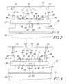
- FIG. 2 The operation of the projecting from the respective subcarrier 28 positioning 36 is in FIG. 2 clarified.
- sections of the heat sink 26, the substrate 12, the projecting away from the heat sink 26 and the substrate 12 enclosing frame 24 and a contact lug 16 of a not shown connecting device with the contacts 18 are also shown schematically.
- a circuit board 40 is in sections with associated with the contacts 18 contact members 42, spaced from the sub-module 10, drawn.
- the printed circuit board 40 is formed with holes 44 whose light cross section is adapted to the cross section of the pin-shaped positioning elements 36.
- the contacts 18 of the contact lug 16 of the sub-module 10 can be laterally offset slightly against the contact members 42 of the circuit board 40 before mounting the circuit board 40 to the circuit arrangement. This offset is indicated by the arrows "a".
- the respective auxiliary carrier 28 is displaced accordingly laterally by the conical centering sections 38 of the pin-shaped positioning elements 36, which. indicated by the arrow 46.
- the contacts 18 of the contact lug 16 and the contact members 42 of the sub-modules 10 common circuit board 40 exactly congruent, ie exactly centered, come into contact. Dimensioning tolerances are thus compensated in a simple manner when the printed circuit board 40 is arranged on the circuit arrangement and contacted with the sub-modules 10.
- the recess 50 is formed in the frame 24 as a transverse slot, so that the subcarrier 28 is not only limitedly movable in the longitudinal direction of the frame 24, but also also perpendicular, i. transverse, this.
- the reference numeral 30 are in FIG. 2 also designates the projecting from the subcarrier 28 pins which extend through the holes 32, which are formed in the associated contact lug 16.
- FIG. 2 has been dispensed with the representation of threaded bushes into which screws are screwed to firmly connect the printed circuit board 40 with the sub-modules 10 correctly positioned and to produce a precisely centered contact between the contacts 18 of the contact lugs 16 and the contact members 42 of the circuit board 40.
- FIG. 3 illustrates schematically in one of FIG. 2 similar representation in sections, a formation of a sub-module 10 with the associated, spaced from the sub-module 10 printed circuit board 40, wherein between the subcarrier 28 and the associated contact lug 16, a cushion member 52 is provided, through which the contact-Anpreßtik between the Kotakten 18 of the contact lug 16 and the contact members 42 of the printed circuit board 42 is further improved when the printed circuit board 40 is attached to the circuit arrangement.
Landscapes
- Engineering & Computer Science (AREA)
- Microelectronics & Electronic Packaging (AREA)
- Combinations Of Printed Boards (AREA)
- Coupling Device And Connection With Printed Circuit (AREA)
Description
- Die Erfindung betrifft eine Schaltungsanordnung mit mindestens zwei Teilmoduln, die in einem Gehäuse nebeneinander angeordnet sind, wobei jedes Teilmodul ein Substrat mit Leiterbahnen und mindestens ein hierauf angeordnetes Halbleiterbauelement aufweist, und zur schaltgerechten Kontaktierung des mindestens einen Halbleiterbauelementes eine Verbindungseinrichtung vorgesehen ist.
- Die
DE 10 2006 027 482 B3 offenbart eine Schaltungsanordnung mit einem Substrat mit Leiterbahnen und hierauf schaltungsgerecht angeordneten Halbleiterbauelementen, und mit einer Verbindungseinrichtung, die aus einem Folienverbund aus mindestens zwei elektrisch leitenden Schichten mit jeweils einer dazwischen angeordneten isolierenden Schicht besteht. Mindestens eine der elektrisch leitenden Schichten ist strukturiert und bildet Leiterbahnen aus. Mindestens eine elektrisch leitende Schicht weist erste Kontakteinrichtungen zu Anschlußflächen der Halbleiterbauelemente auf. Mindestens ein Teil dieser und/oder einer weiteren elektrisch leitenden Schicht bildet ein Teil mindestens einer zweiten Kontakteinrichtung zur reversiblen Verbindung mit einer externen Zuleitung. Die zweite Kontakteinrichtung weist mindestens ein Federelement mit einem Widerlager eines Gehäuses und/oder mindestens eine Feststellschraube auf. - Die
DE 10 2009 024 385 beschreibt ein Leistungshalbleitermodul mit einem Substrat, einer Verbindungseinrichtung und mit Lastanschlußelementen, wobei auf einer Leiterbahn des Substrates mindestens ein Halbleiterbauelement angeordnet und schaltungsgerecht mittels der Verbindungseinrichtung aus einer Schichtfolge mit einer strukturierten ersten elektrisch leitenden Metallfolie, einer elektrisch isolierenden Folie und einer strukturierten zweiten elektrisch leitenden Folie mit mindestens einem Lastanschlußelement verbunden ist, wobei mindestens eine erste Leiterbahn eine Kontaktfläche aufweist, die mit einem Lastanschlußelement stoffschlüssig verbunden ist, und wobei die Verbindungseinrichtung Hilfskontakt-Anschlußflächen aufweist, die mit einer externen Leiterplatte verbindbar sind. - Aus der
WO 2007/079534 A1 ist ein Untersystem für eine Computereinrichtung bekannt, die mehrere auf einen faltbaren Substrat angeordnete Chips aufweist. - Aus der
US 2004/0246662 A1 ist ein Powermodul für Hochfrequenzschaltsysteme bekannt, bei dem ein eine ebene Fläche aufweisender Kühlkörper mit einer auf einer keramischen Schicht angeordneten metallischen Schicht verlötet ist. - Aus der
US 2006/0119761 A1 ist ein Display mit einem Rahmen und einer Leiterplatte bekannt. - Aus der
2005/0233611 A1 - Aus der
DE 20 2008 052 029 A1 ist ein Halbleitermodul bekannt, das wenigstens einen Halbleiterchip, der auf einem Trägersubstrat angeordnet ist, aufweist. Das Halbleitermodul hat ein Gehäuse in dem das Trägersubstrat und eine Platine übereinander angeordnet sind, wobei die Platine eine sichere galvanische Trennung aufweist. - Bei Schaltungsanordnungen mit mindestens zwei Teilmoduln, die in einem Gehäuse nebeneinander angeordnet sind, ergibt sich für die Anbindung der Hilfskontakte an eine gemeinsame Leiterplatte zwischen dem jeweiligen Teilmodul und der Leiterplatte eine kritische Toleranz-Kette.
- Der Erfindung liegt deshalb die Aufgabe zugrunde, eine Schaltungsanordnung der eingangs genannten Art zu schaffen, wobei die erwähnte kritische Toleranz-Kette zwischen den Teilmoduln und der gemeinsamen Leiterplatte eliminiert ist.
- Diese Aufgabe wird erfindungsgemäß durch die Merkmale des Anspruches 1 gelöst. Bevorzugte Aus- bzw. Weiterbildungen der erfindungsgemäßen Schaltungsanordnung sind in den Unteransprüchen gekennzeichnet.
- Erfindungsgemäß weist die Verbindungseinrichtung, zu dem jeweiligen Teilmodul zugehörig, mindestens eine Kontaktfahne mit Kontakten zur Kontaktierung mit Kontaktorganen der gemeinsamen Leiterplatte auf. Jedes Teilmodul weist einen Rahmen auf, der das zugehörige Substrat umschließt. Der Rahmen besteht vorzugsweise aus einem elektrisch isolierenden Material. An dem jeweiligen Rahmen ist mindestens ein Hilfsträger begrenzt beweglich vorgesehen, an dem die zugehörige Kontaktfahne befestigt ist. Diese Befestigung kann durch einen Formschluß und/oder durch einen Kraftschluß und/oder durch einen Materialschluß realisiert sein.
- Der mindestens eine Hilfsträger für die zugehörige Kontaktfahne der jeweiligen Verbindungseinrichtung weist mindestens ein Positionierelement auf, das zur positionsgenauen Ausrichtung der Kontakte der entsprechenden Kontaktfahne relativ zu den Kontaktorganen der Leiterplatte vorgesehen ist, wenn die Leiterplatte an der erfindungsgemäßen Schaltungsanordnung angeordnet wird. Mit Hilfe der Positionierelemente werden die Hilfsträger mit den an ihnen befestigten Kontaktfahnen der flexiblen Verbindungseinrichtungen der Teilmodule genau richtig in Bezug zu den Kontaktorganen der Leiterplatte ausgerichtet, wenn diese an der Schaltungsanordnung angebracht und mit den Teilmoduln kontaktiert wird.
- Erfindungsgemäß ist der mindestens eine Hilfsträger am Rahmen des entsprechenden Teilmoduls in Rahmen-Längsrichtung begrenzt beweglich. Außerdem ist der mindestens eine Hilfsträger am Rahmen auch senkrecht zur Rahmen-Längsrichtung begrenzt beweglich.
- Der jeweilige Hilfsträger weist für die zugehörige Kontaktfahne zweckmäßigerweise eine ebene Auflagefläche auf, um zu den Kontaktorganen der Leiterplatte ein definiertes Gegenlager zu bilden. Zweckmäßig kann es sein, wenn zwischen dem mindestens einen Hilfsträger und der zugehörigen Kontaktfahne der flexiblen Verbindungseinrichtung des jeweiligen Teilmoduls ein flexibles Polsterelement vorgesehen ist, durch das der Kontakt-Anpreßdruck zwischen den Kontakten der Kontaktfahne und den Kontaktorganen der den Teilmoduln zugeordneten Leiterplatte weiter verbessert wird.
- Das mindestens eine Positionierelement des jeweiligen Hilfsträgers ist vorzugsweise stiftförmig mit einem sich verjüngenden Zentrierabschnitt ausgebildet. Mit Hilfe des Zentrierabschnittes erfolgt automatisch eine Selbstzentrierung des jeweiligen Hilfsträgers in Bezug zur gemeinsamen Leiterplatte und somit eine Selbstzentrierung der Kontakte der Kontaktfahnen der flexiblen Verbindungseinrichtungen der Teilmodule in Bezug zu den zugehörigen Kontaktorganen der gemeinsamen Leiterplatte.
- Die Hilfsträger der Teilmodule weisen zur Befestigung der gemeinsamen Leiterplatte zweckmäßigerweise Befestigungsorgane auf. Bei den Befestigungsorganen handelt sich beispielsweise um Gewindebuchsen, die zur Schraubbefestigung der Leiterplatte vorgesehen sind. Die Befestigungsorgane können z.B. auch als Schnapp-Rast-Elemente, als Klemmelemente o.dgl. ausgebildet sein.
- Grundsätzlich wäre es auch möglich, den Erfindungsgedanken bei einem einzigen Modul anstelle mindestens zweier Teilmodule anzuwenden.
- Weitere Einzelheiten, Merkmale und Vorteile ergeben sich aus der nachfolgenden Beschreibung in Verbindung mit den anliegenden Zeichnungen.
- Es zeigen:
-
Figur 1 ein Teilmodul der Schaltungsanordnung in einer perspektivischen Ansicht, -
Figur 2 schematisch abschnittweise in einer Seitenansicht wesentliche Einzelheiten eines Teilmoduls sowie einer davon beabstandet gezeichneten Leiterplatte, und -
Figur 3 eine derFigur 2 ähnliche schematische Darstellung einer Ausbildung mit einem Polsterelement zwischen der Kontaktfahne und dem Hilfsträger. -
Figur 1 zeigt ein Teilmodul 10 einer erfindungsgemäßen Schaltungsanordnung, die in einem nicht gezeichneten Gehäuse nebeneinander mindestens zwei solche Teilmodule aufweist. Das jeweilige Teilmodul 10 weist ein Substrat 12 mit Leiterbahnen 14 und hierauf angeordneten (nicht gezeichneten) Halbleiterbauelementen auf. Zur Kontaktierung der Halbleiterbauelemente ist eine Verbindungseinrichtung vorgesehen, die Kontaktfahnen 16 mit Kontakten 18 aufweist. Bei den Kontakten 18 handelt es sich z.B. um Hilfskontakte des Teilmoduls 10. Mit der Bezugsziffer 20 sind Gleichstrom-Lastanschlüsse und mit der Bezugsziffer 22 ist ein Wechselstrom-Lastanschluß des Teilmoduls 10 bezeichnet. Das Teilmodul 10 bildet somit beispielsweise einen Umrichter. Selbstverständlich kann es sich bei dem Teilmodul 10 auch um ein Teilmodul für eine andere Schaltungsanordnung handeln. - Das Teilmodul 10 weist einen Rahmen 24 auf, der das zugehörige Substrat 12 umschließt. Der Rahmen 24 besteht aus einem elektrisch isolierenden Material, er steht von einem Kühlkörper 26 des Teilmoduls 10 nach oben. Der Kühlkörper 26 besteht aus Metall, beispielsweise aus Aluminium oder einer Aluminiumlegierung.
- Am Rahmen 24 sind einander gegenüberliegend zwei Hilfsträger 28 begrenzt beweglich in Längsrichtung des Rahmens 24 und hierzu senkrecht, d.h. quer zur Rahmenlängsrichtung begrenzt beweglich vorgesehen. Die Kontaktfahne 16 der Verbindungseinrichtung ist am zugehörigen Hilfsträger 28 befestigt. Zu diesem Zwecke stehen von der ebenen Oberseite des jeweiligen Hilfsträgers 28 materialeinstückig Zapfen 30 weg, die sich durch Löcher 32 erstrecken, die in der jeweiligen Kontaktfahne 16 ausgebildet sind. Zur Fixierung der Kontaktfahne 16 am zugehörigen Hilfsträger 28 sind die Zapfe 30 beispielsweise heiß verstemmt.
- Die Befestigung der Kontaktfahnen 16 an den jeweils zugehörigen Hilfsträgern 28 kann beispielsweise auch durch Verrastung, durch Festklemmen o.dgl. erfolgen.
- Vom jeweiligen Hilfsträger 28 stehen materialeinstückig außerdem Befestigungsorgane 34 für die Leiterplatte und stiftförmige Positionierelemente 36 weg. Die Befestigungsorgane sind als Gewindebuchsen ausgebildet. Die Positionierelemente 36 sind mit verjüngten Zentrierabschnitten 38 ausgebildet. Die Zentrierabschnitte 38 können konisch, ballig oder beliebig anders verjüngt geformt sein.
- Die Funktionsweise der vom jeweiligen Hilfsträger 28 wegstehenden Positionierelemente 36 ist in
Figur 2 verdeutlicht. In dieser Figur sind außerdem abschnittweise der Kühlkörper 26, das Substrat 12, der vom Kühlkörper 26 wegstehende und das Substrat 12 umschließende Rahmen 24 sowie eine Kontaktfahne 16 einer nicht gezeichneten Verbindungseinrichtung mit den Kontakten 18 schematisch dargestellt. Außerdem ist abschnittweise eine Leiterplatte 40 mit zu den Kontakten 18 zugehörigen Kontaktorganen 42, vom Teilmodul 10 beabstandet, gezeichnet. Die Leiterplatte 40 ist mit Löchern 44 ausgebildet, deren lichter Querschnitt an den Querschnitt der stiftförmigen Positionierelemente 36 angepaßt ist. - Bedingt durch Abmessungstoleranzen können die Kontakte 18 der Kontaktfahne 16 des Teilmoduls 10 gegen die Kontaktorgane 42 der Leiterplatte 40 vor der Montage der Leiterplatte 40 an der Schaltungsanordnung seitlich geringfügig versetzt sein. Dieser Versatz ist durch die Pfeile "a" verdeutlicht.
- Wird die Leiterplatte 40 an der Schaltungsanordnung angeordnet, so wird der jeweilige Hilfsträger 28 durch die konischen Zentrierabschnitte 38 der stiftförmigen Positionierelemente 36 entsprechend seitlich verschoben, was . durch den Pfeil 46 angedeutet ist. Dabei kommen die Kontakte 18 der Kontaktfahne 16 und die Kontaktorgane 42 der den Teilmodulen 10 gemeinsamen Leiterplatte 40 genau deckungsgleich, d.h. genau zentriert, miteinander in Kontakt. Abessungstoleranzen werden also in einfacher Weise ausgeglichen, wenn die Leiterplatte 40 an der Schaltungsanordnung angeordnet und mit den Teilmoduln 10 kontaktiert wird.
- Zur begrenzten Beweglichkeit der jeweiligen Hilfsträgers 28 steht von dessen Unterseite ein Ansatz 48 weg, der in eine Aussparung 50 hineinragt, die im Rahmen 24 ausgebildet ist.
- Die Aussparung 50 ist im Rahmen 24 als Querschlitz ausgebildet, so dass der Hilfsträger 28 nicht nur in Längsrichtung des Rahmens 24 begrenzt beweglich ist, sondern außerdem auch senkrecht, d.h. quer, hierzu.
- Mit der Bezugsziffer 30 sind in
Figur 2 auch die vom Hilfsträger 28 wegstehenden Zapfen bezeichnet, die sich durch die Löcher 32 hindurch erstrecken, die in der zugehörigen Kontaktfahne 16 ausgebildet sind. InFigur 2 ist auf die Darstellung von Gewindebuchsen verzichtet worden, in welche Schrauben eingeschraubt werden, um die Leiterplatte 40 mit den Teilmodulen 10 richtig positioniert fest zu verbinden und einen genau zentrierten Kontakt zwischen den Kontakten 18 der Kontaktfahnen 16 und den Kontaktorganen 42 der Leiterplatte 40 herzustellen. -
Figur 3 verdeutlicht schematisch in einer derFigur 2 ähnlichen Darstellung abschnittweise eine Ausbildung eines Teilmoduls 10 mit der zugehörigen, vom Teilmodul 10 beabstandet gezeichneten Leiterplatte 40, wobei zwischen dem Hilfsträger 28 und der zugehörigen Kontaktfahne 16 ein Polsterelement 52 vorgesehen ist, durch welches der Kontakt-Anpreßdruck zwischen den Kotakten 18 der Kontaktfahne 16 und den Kontaktorganen 42 der Leiterplatte 42 weiter verbessert wird, wenn die Leiterplatte 40 an der Schaltungsanordnung befestigt wird. - Gleiche Einzelheiten sind in den Figuren jeweils mit denselben Bezugsziffern bezeichnet, so dass es sich erübrigt, in Verbindung mit den Figuren alle Einzelheiten jeweils detailliert zu beschreiben.
-
- 10
- Teilmodul (einer Schaltungsanordnung)
- 12
- Substrat (von 10)
- 14
- Leiterbahnen (an 12)
- 16
- Kontaktfahne (für 18)
- 18
- Kontakte (an 16)
- 20
- Gleichstrom-Lastanschlüsse (von 10)
- 22
- Wechselstrom-Lastanschluß (von 10)
- 24
- Rahmen (von 10 an 26 für 28)
- 26
- Kühlkörper (von 10)
- 28
- Hilfsträger (für 16)
- 30
- Zapfen (an 28 für 16)
- 32
- Löcher (in 16 bzw. 52 für 30)
- 34
- Befestigungsorgan (an 28 für 40)
- 36
- Positionierelemente (an 28 für 40)
- 38
- Zentrierabschnitt (von 36)
- 40
- Leiterplatte (für 10)
- 42
- Kontaktorgane (an 40)
- 44
- Loch (in 40 für 36)
- 46
- Pfeil (bei 28)
- 48
- Ansatz (an 28 in 50)
- 50
- Aussparung (in 24 für 48)
- 52
- Posterelement (zwischen 16 und 28)
Claims (6)
- Schaltungsanordnung mit mindestens zwei Teilmoduln (10), die in einem Gehäuse nebeneinander angeordnet sind und mit einer Leiterplatte (40), wobei die Teilmodule Gleichstrom-Lastanschlüsse und einen Wechselstrom-Lastanschluss aufweisen, wobei jedes Teilmodul (10) ein Substrat (12) mit Leiterbahnen (16) und mindestens ein hierauf angeordnetes Halbleiterbauelement aufweist, und zur schaltgerechten Kontaktierung des mindestens einen Halbleiterbauelementes eine Verbindungseinrichtung vorgesehen ist, die mindestens eine Kontaktfahne (16) mit Kontakten (18) zur Kontaktierung mit Kontaktorganen (42) der Leiterplatte (40) aufweist, die den mindestens zwei Teilmoduln (10) zugeordnet ist, wobei jedes Teilmodul (10) einen das zugehörige Substrat (12) umschließenden Rahmen (24) aufweist, an dem mindestens ein Hilfsträger (28) in Rahmen-Längsrichtung begrenzt beweglich angeordnet ist, an dem die zugehörige Kontaktfahne (16) befestigt ist, wobei zur begrenzten Beweglichkeit des jeweiligen Hilfsträgers (28) von dessen Unterseite ein Ansatz (48) weg steht, der in eine Aussparung (50) hineinragt, die im Rahmen (24) als Querschlitz ausgebildet ist, wobei der mindestens eine Hilfsträger (28) mindestens ein Positionierelement (36) aufweist, das zur positionsgenauen Ausrichtung und Zentrierung der Kontakte (18) der entsprechenden Kontaktfahne (16) in Bezug zu den Kontaktorganen (42) der den Teilmoduln (10) gemeinsamen Leiterplatte (40) vorgesehen ist.
- Schaltungsanordnung nach Anspruch 1,
dadurch gekennzeichnet,
dass die Kontaktfahne (16) am zugehörigen Hilfsträger (28) formschlüssig oder kraftschlüssig oder materialschlüssig befestigt ist. - Schaltungsanordnung nach Anspruch 1,
dadurch gekennzeichnet,
dass der mindestens eine Hilfsträger (28) am zugehörigen Rahmen (24) auch in Richtung senkrecht zur Rahmen-Längsrichtung begrenzt beweglich ist. - Schaltungsanordnung nach einem der Ansprüche 1 bis 3,
dadurch gekennzeichnet,
dass zwischen dem mindestens einen Hilfsträger (28) und der zugehörigen Kontaktfahne (16) des jeweiligen Teilmoduls (10) ein Polsterelement (52) vorgesehen ist. - Schaltungsanordnung nach Anspruch 1,
dadurch gekennzeichnet,
dass das mindestens eine Positionierelement (36) des jeweiligen Hilfsträgers (28) stiftförmig mit einem sich verjüngenden Zentrierabschnitt (38) ausgebildet ist. - Schaltungsanordnung nach einem der Ansprüche 1 bis 5,
dadurch gekennzeichnet,
dass der jeweilige Hilfsträger (28) zur Befestigung der Leiterplatte (40) mindestens ein Befestigungsorgan (34) aufweist.
Applications Claiming Priority (1)
| Application Number | Priority Date | Filing Date | Title |
|---|---|---|---|
| DE102010063387A DE102010063387A1 (de) | 2010-12-17 | 2010-12-17 | Schaltungsanordnung mit mindestens zwei Teilmoduln |
Publications (2)
| Publication Number | Publication Date |
|---|---|
| EP2467001A1 EP2467001A1 (de) | 2012-06-20 |
| EP2467001B1 true EP2467001B1 (de) | 2014-08-27 |
Family
ID=45524242
Family Applications (1)
| Application Number | Title | Priority Date | Filing Date |
|---|---|---|---|
| EP20110188754 Active EP2467001B1 (de) | 2010-12-17 | 2011-11-11 | Schaltungsanordnung mit mindestens zwei Teilmoduln |
Country Status (3)
| Country | Link |
|---|---|
| EP (1) | EP2467001B1 (de) |
| CN (1) | CN102548208B (de) |
| DE (1) | DE102010063387A1 (de) |
Families Citing this family (6)
| Publication number | Priority date | Publication date | Assignee | Title |
|---|---|---|---|---|
| DE102013100701B4 (de) | 2013-01-24 | 2022-07-21 | Infineon Technologies Ag | Halbleitermodulanordnung und verfahren zur herstellung einer halbleitermodulanordnung |
| DE102013100700B3 (de) * | 2013-01-24 | 2014-05-15 | Infineon Technologies Ag | Verfahren zur herstellung einer halbleitermodulanordnung |
| FR3024319B1 (fr) * | 2014-07-23 | 2018-04-27 | Valeo Equipements Electriques Moteur | Dispositif electronique d'un compresseur de suralimentation electrique |
| EP4213202B1 (de) * | 2022-01-17 | 2024-02-28 | Siemens Aktiengesellschaft | Leistungsmodul |
| WO2023213346A1 (de) * | 2022-05-06 | 2023-11-09 | Fachhochschule Kiel | Leistungshalbleiter-modul mit steckverbindung |
| DE102022205358A1 (de) | 2022-05-30 | 2023-11-30 | Robert Bosch Gesellschaft mit beschränkter Haftung | Elektronische Baugruppe, insbesondere eine elektronische Leistungsbaugruppe für Hybridfahrzeuge oder Elektrofahrzeuge |
Family Cites Families (14)
| Publication number | Priority date | Publication date | Assignee | Title |
|---|---|---|---|---|
| US6442027B2 (en) * | 2000-02-23 | 2002-08-27 | Denso Corporation | Electronic control unit having connector positioned between two circuit substrates |
| US6365434B1 (en) * | 2000-06-28 | 2002-04-02 | Micron Technology, Inc. | Method and apparatus for reduced flash encapsulation of microelectronic devices |
| DE10103456C1 (de) * | 2001-01-25 | 2002-08-29 | Infineon Technologies Ag | Vorrichtung mit mindestens einem Halbleiterbauteil und einer Leiterplatte und Verfahren zur Herstellung einer elektromechanischen Verbindung zwischen beiden |
| DE10110620A1 (de) * | 2001-03-06 | 2002-09-26 | Conti Temic Microelectronic | Elekronische Baugruppe |
| US6849943B2 (en) * | 2003-06-06 | 2005-02-01 | Electronic Theatre Controls, Inc. | Power module package for high frequency switching system |
| TWI249717B (en) * | 2004-04-19 | 2006-02-21 | Au Optronics Corp | Signal transmission device |
| FR2872992B1 (fr) * | 2004-07-09 | 2006-09-29 | Valeo Vision Sa | Assemblage electronique a drain thermique notamment pour module de commande de lampe a decharge de projecteurs de vehicule automobile |
| JP2006157487A (ja) * | 2004-11-30 | 2006-06-15 | Sanyo Electric Co Ltd | 表示装置および携帯電話 |
| WO2007079534A1 (en) * | 2006-01-12 | 2007-07-19 | Para Kanagasabai Segaram | A subsystem for computing devices |
| DE102006027482B3 (de) | 2006-06-14 | 2007-08-16 | Semikron Elektronik Gmbh & Co. Kg | Gehauste Halbleiterschaltungsanordnung mit Kontakteinrichtung |
| DE102006027748A1 (de) * | 2006-06-16 | 2007-12-20 | Robert Bosch Gmbh | Leiterplatte und Verfahren zur Herstellung einer lötfreien elektrischen Verbindung |
| US7291023B1 (en) * | 2006-11-21 | 2007-11-06 | Autoliv Asp, Inc. | Electric vehicle motion sensor |
| US7800222B2 (en) * | 2007-11-29 | 2010-09-21 | Infineon Technologies Ag | Semiconductor module with switching components and driver electronics |
| DE102009024385B4 (de) | 2009-06-09 | 2011-03-17 | Semikron Elektronik Gmbh & Co. Kg | Verfahren zur Herstellung eines Leistungshalbleitermoduls und Leistungshalbleitermodul mit einer Verbindungseinrichtung |
-
2010
- 2010-12-17 DE DE102010063387A patent/DE102010063387A1/de not_active Withdrawn
-
2011
- 2011-11-11 EP EP20110188754 patent/EP2467001B1/de active Active
- 2011-12-16 CN CN201110424561.0A patent/CN102548208B/zh active Active
Also Published As
| Publication number | Publication date |
|---|---|
| CN102548208B (zh) | 2016-03-23 |
| CN102548208A (zh) | 2012-07-04 |
| EP2467001A1 (de) | 2012-06-20 |
| DE102010063387A1 (de) | 2012-06-21 |
Similar Documents
| Publication | Publication Date | Title |
|---|---|---|
| EP1255299B1 (de) | Leistungshalbleitermodul in Druckkontaktierung | |
| EP1450404B1 (de) | Anordnung in Druckkontaktierung mit einem Leistungshalbleitermodul | |
| EP0920055B1 (de) | Kühlvorrichtung für ein auf einer Leiterplatte angeordnetes, wärmeerzeugendes Bauelement | |
| EP1898466B1 (de) | Gehauste Halbleiterschaltungsanordnung mit Kontakteinrichtung | |
| DE112016005794B4 (de) | Schaltungsanordnung und elektrischer Anschlusskasten | |
| DE102009046403B4 (de) | Leistungshalbleitermodul in Druckkontakttechnik | |
| DE112006002302B4 (de) | Elektrisches system umfassend eine leistungstransistoranordnung, eine stromschiene und eine leiterplattenbaugruppe | |
| EP1831055A1 (de) | Steuermodul | |
| EP0588793A1 (de) | Gehäuse für kfz-elektronik. | |
| DE102012208146A1 (de) | Verbindungssystem zur herstellung elektrischer verbindungen eines leistungshalbleitermoduls und verfahren zur herstellung solcher verbindungen | |
| WO2014135373A1 (de) | Elektronische, optoelektronische oder elektrische anordnung | |
| EP2467001A1 (de) | Schaltungsanordnung mit mindestens zwei Teilmoduln | |
| WO2011113867A1 (de) | Schaltungseinheit mit stromschiene zur strom- und wärmeübertragung sowie ein verfahren zur herstellung dieser schaltungseinheit | |
| EP3053192B1 (de) | Schaltungsvorrichtung und verfahren zu deren herstellung | |
| DE102011080153A1 (de) | Flexible verbindung von substraten in leistungshalbleitermodulen | |
| EP1926637A2 (de) | Kombiniertes befestigungs- und kontaktierungssystem für elektrische bauelemente auf übereinander angeordneten leiterplatten | |
| DE102015219851B4 (de) | Steuergerät | |
| DE10340297B4 (de) | Verbindugsanordnung zur Verbindung von aktiven und passiven elektrischen und elektronischen Bauelementen | |
| EP0489958B1 (de) | Leiterplatte für elektronische Steuergeräte und Verfahren zum Herstellen einer solchen Leiterplatte | |
| DE102006008807B4 (de) | Anordnung mit einem Leistungshalbleitermodul und einem Kühlbauteil | |
| DE102017211336B4 (de) | Leistungsmodul mit oberflächenmontierten elektrischen Kontaktierungselementen | |
| DE102007039618B4 (de) | Modul für eine integrierte Steuerelektronik mit vereinfachtem Aufbau | |
| DE19805492C2 (de) | Leiterplatte | |
| EP3841854A1 (de) | Verfahren für eine montage eines elektrischen geräts und zugehöriges elektrisches gerät | |
| WO2019219637A1 (de) | Leiterplattenaufbau zur aufnahme wenigstens eines halbleiterleuchtmittels |
Legal Events
| Date | Code | Title | Description |
|---|---|---|---|
| PUAI | Public reference made under article 153(3) epc to a published international application that has entered the european phase |
Free format text: ORIGINAL CODE: 0009012 |
|
| 17P | Request for examination filed |
Effective date: 20120403 |
|
| AK | Designated contracting states |
Kind code of ref document: A1 Designated state(s): AL AT BE BG CH CY CZ DE DK EE ES FI FR GB GR HR HU IE IS IT LI LT LU LV MC MK MT NL NO PL PT RO RS SE SI SK SM TR |
|
| AX | Request for extension of the european patent |
Extension state: BA ME |
|
| 17Q | First examination report despatched |
Effective date: 20140109 |
|
| GRAP | Despatch of communication of intention to grant a patent |
Free format text: ORIGINAL CODE: EPIDOSNIGR1 |
|
| INTG | Intention to grant announced |
Effective date: 20140604 |
|
| GRAS | Grant fee paid |
Free format text: ORIGINAL CODE: EPIDOSNIGR3 |
|
| GRAA | (expected) grant |
Free format text: ORIGINAL CODE: 0009210 |
|
| AK | Designated contracting states |
Kind code of ref document: B1 Designated state(s): AL AT BE BG CH CY CZ DE DK EE ES FI FR GB GR HR HU IE IS IT LI LT LU LV MC MK MT NL NO PL PT RO RS SE SI SK SM TR |
|
| REG | Reference to a national code |
Ref country code: GB Ref legal event code: FG4D Free format text: NOT ENGLISH |
|
| REG | Reference to a national code |
Ref country code: CH Ref legal event code: EP |
|
| REG | Reference to a national code |
Ref country code: AT Ref legal event code: REF Ref document number: 685049 Country of ref document: AT Kind code of ref document: T Effective date: 20140915 |
|
| REG | Reference to a national code |
Ref country code: IE Ref legal event code: FG4D Free format text: LANGUAGE OF EP DOCUMENT: GERMAN |
|
| REG | Reference to a national code |
Ref country code: DE Ref legal event code: R096 Ref document number: 502011004178 Country of ref document: DE Effective date: 20141009 |
|
| REG | Reference to a national code |
Ref country code: LT Ref legal event code: MG4D |
|
| REG | Reference to a national code |
Ref country code: NL Ref legal event code: VDEP Effective date: 20140827 |
|
| PG25 | Lapsed in a contracting state [announced via postgrant information from national office to epo] |
Ref country code: GR Free format text: LAPSE BECAUSE OF FAILURE TO SUBMIT A TRANSLATION OF THE DESCRIPTION OR TO PAY THE FEE WITHIN THE PRESCRIBED TIME-LIMIT Effective date: 20141128 Ref country code: FI Free format text: LAPSE BECAUSE OF FAILURE TO SUBMIT A TRANSLATION OF THE DESCRIPTION OR TO PAY THE FEE WITHIN THE PRESCRIBED TIME-LIMIT Effective date: 20140827 Ref country code: LT Free format text: LAPSE BECAUSE OF FAILURE TO SUBMIT A TRANSLATION OF THE DESCRIPTION OR TO PAY THE FEE WITHIN THE PRESCRIBED TIME-LIMIT Effective date: 20140827 Ref country code: SE Free format text: LAPSE BECAUSE OF FAILURE TO SUBMIT A TRANSLATION OF THE DESCRIPTION OR TO PAY THE FEE WITHIN THE PRESCRIBED TIME-LIMIT Effective date: 20140827 Ref country code: NO Free format text: LAPSE BECAUSE OF FAILURE TO SUBMIT A TRANSLATION OF THE DESCRIPTION OR TO PAY THE FEE WITHIN THE PRESCRIBED TIME-LIMIT Effective date: 20141127 Ref country code: BG Free format text: LAPSE BECAUSE OF FAILURE TO SUBMIT A TRANSLATION OF THE DESCRIPTION OR TO PAY THE FEE WITHIN THE PRESCRIBED TIME-LIMIT Effective date: 20141127 Ref country code: ES Free format text: LAPSE BECAUSE OF FAILURE TO SUBMIT A TRANSLATION OF THE DESCRIPTION OR TO PAY THE FEE WITHIN THE PRESCRIBED TIME-LIMIT Effective date: 20140827 Ref country code: PT Free format text: LAPSE BECAUSE OF FAILURE TO SUBMIT A TRANSLATION OF THE DESCRIPTION OR TO PAY THE FEE WITHIN THE PRESCRIBED TIME-LIMIT Effective date: 20141229 |
|
| PG25 | Lapsed in a contracting state [announced via postgrant information from national office to epo] |
Ref country code: HR Free format text: LAPSE BECAUSE OF FAILURE TO SUBMIT A TRANSLATION OF THE DESCRIPTION OR TO PAY THE FEE WITHIN THE PRESCRIBED TIME-LIMIT Effective date: 20140827 Ref country code: RS Free format text: LAPSE BECAUSE OF FAILURE TO SUBMIT A TRANSLATION OF THE DESCRIPTION OR TO PAY THE FEE WITHIN THE PRESCRIBED TIME-LIMIT Effective date: 20140827 Ref country code: LV Free format text: LAPSE BECAUSE OF FAILURE TO SUBMIT A TRANSLATION OF THE DESCRIPTION OR TO PAY THE FEE WITHIN THE PRESCRIBED TIME-LIMIT Effective date: 20140827 Ref country code: IS Free format text: LAPSE BECAUSE OF FAILURE TO SUBMIT A TRANSLATION OF THE DESCRIPTION OR TO PAY THE FEE WITHIN THE PRESCRIBED TIME-LIMIT Effective date: 20141227 Ref country code: CY Free format text: LAPSE BECAUSE OF FAILURE TO SUBMIT A TRANSLATION OF THE DESCRIPTION OR TO PAY THE FEE WITHIN THE PRESCRIBED TIME-LIMIT Effective date: 20140827 |
|
| PG25 | Lapsed in a contracting state [announced via postgrant information from national office to epo] |
Ref country code: NL Free format text: LAPSE BECAUSE OF FAILURE TO SUBMIT A TRANSLATION OF THE DESCRIPTION OR TO PAY THE FEE WITHIN THE PRESCRIBED TIME-LIMIT Effective date: 20140827 |
|
| PG25 | Lapsed in a contracting state [announced via postgrant information from national office to epo] |
Ref country code: CZ Free format text: LAPSE BECAUSE OF FAILURE TO SUBMIT A TRANSLATION OF THE DESCRIPTION OR TO PAY THE FEE WITHIN THE PRESCRIBED TIME-LIMIT Effective date: 20140827 Ref country code: DK Free format text: LAPSE BECAUSE OF FAILURE TO SUBMIT A TRANSLATION OF THE DESCRIPTION OR TO PAY THE FEE WITHIN THE PRESCRIBED TIME-LIMIT Effective date: 20140827 Ref country code: SK Free format text: LAPSE BECAUSE OF FAILURE TO SUBMIT A TRANSLATION OF THE DESCRIPTION OR TO PAY THE FEE WITHIN THE PRESCRIBED TIME-LIMIT Effective date: 20140827 Ref country code: EE Free format text: LAPSE BECAUSE OF FAILURE TO SUBMIT A TRANSLATION OF THE DESCRIPTION OR TO PAY THE FEE WITHIN THE PRESCRIBED TIME-LIMIT Effective date: 20140827 Ref country code: RO Free format text: LAPSE BECAUSE OF FAILURE TO SUBMIT A TRANSLATION OF THE DESCRIPTION OR TO PAY THE FEE WITHIN THE PRESCRIBED TIME-LIMIT Effective date: 20140827 Ref country code: IT Free format text: LAPSE BECAUSE OF FAILURE TO SUBMIT A TRANSLATION OF THE DESCRIPTION OR TO PAY THE FEE WITHIN THE PRESCRIBED TIME-LIMIT Effective date: 20140827 |
|
| REG | Reference to a national code |
Ref country code: DE Ref legal event code: R097 Ref document number: 502011004178 Country of ref document: DE |
|
| PG25 | Lapsed in a contracting state [announced via postgrant information from national office to epo] |
Ref country code: PL Free format text: LAPSE BECAUSE OF FAILURE TO SUBMIT A TRANSLATION OF THE DESCRIPTION OR TO PAY THE FEE WITHIN THE PRESCRIBED TIME-LIMIT Effective date: 20140827 |
|
| PG25 | Lapsed in a contracting state [announced via postgrant information from national office to epo] |
Ref country code: BE Free format text: LAPSE BECAUSE OF NON-PAYMENT OF DUE FEES Effective date: 20141130 Ref country code: MC Free format text: LAPSE BECAUSE OF FAILURE TO SUBMIT A TRANSLATION OF THE DESCRIPTION OR TO PAY THE FEE WITHIN THE PRESCRIBED TIME-LIMIT Effective date: 20140827 Ref country code: LU Free format text: LAPSE BECAUSE OF FAILURE TO SUBMIT A TRANSLATION OF THE DESCRIPTION OR TO PAY THE FEE WITHIN THE PRESCRIBED TIME-LIMIT Effective date: 20141111 |
|
| REG | Reference to a national code |
Ref country code: CH Ref legal event code: PL |
|
| PLBE | No opposition filed within time limit |
Free format text: ORIGINAL CODE: 0009261 |
|
| STAA | Information on the status of an ep patent application or granted ep patent |
Free format text: STATUS: NO OPPOSITION FILED WITHIN TIME LIMIT |
|
| PG25 | Lapsed in a contracting state [announced via postgrant information from national office to epo] |
Ref country code: CH Free format text: LAPSE BECAUSE OF NON-PAYMENT OF DUE FEES Effective date: 20141130 Ref country code: LI Free format text: LAPSE BECAUSE OF NON-PAYMENT OF DUE FEES Effective date: 20141130 |
|
| 26N | No opposition filed |
Effective date: 20150528 |
|
| REG | Reference to a national code |
Ref country code: IE Ref legal event code: MM4A |
|
| PG25 | Lapsed in a contracting state [announced via postgrant information from national office to epo] |
Ref country code: IE Free format text: LAPSE BECAUSE OF NON-PAYMENT OF DUE FEES Effective date: 20141111 |
|
| REG | Reference to a national code |
Ref country code: FR Ref legal event code: PLFP Year of fee payment: 5 |
|
| PG25 | Lapsed in a contracting state [announced via postgrant information from national office to epo] |
Ref country code: SI Free format text: LAPSE BECAUSE OF FAILURE TO SUBMIT A TRANSLATION OF THE DESCRIPTION OR TO PAY THE FEE WITHIN THE PRESCRIBED TIME-LIMIT Effective date: 20140827 |
|
| PG25 | Lapsed in a contracting state [announced via postgrant information from national office to epo] |
Ref country code: SM Free format text: LAPSE BECAUSE OF FAILURE TO SUBMIT A TRANSLATION OF THE DESCRIPTION OR TO PAY THE FEE WITHIN THE PRESCRIBED TIME-LIMIT Effective date: 20140827 |
|
| PG25 | Lapsed in a contracting state [announced via postgrant information from national office to epo] |
Ref country code: MT Free format text: LAPSE BECAUSE OF FAILURE TO SUBMIT A TRANSLATION OF THE DESCRIPTION OR TO PAY THE FEE WITHIN THE PRESCRIBED TIME-LIMIT Effective date: 20140827 Ref country code: TR Free format text: LAPSE BECAUSE OF FAILURE TO SUBMIT A TRANSLATION OF THE DESCRIPTION OR TO PAY THE FEE WITHIN THE PRESCRIBED TIME-LIMIT Effective date: 20140827 Ref country code: HU Free format text: LAPSE BECAUSE OF FAILURE TO SUBMIT A TRANSLATION OF THE DESCRIPTION OR TO PAY THE FEE WITHIN THE PRESCRIBED TIME-LIMIT; INVALID AB INITIO Effective date: 20111111 |
|
| REG | Reference to a national code |
Ref country code: FR Ref legal event code: PLFP Year of fee payment: 6 |
|
| REG | Reference to a national code |
Ref country code: FR Ref legal event code: PLFP Year of fee payment: 7 |
|
| REG | Reference to a national code |
Ref country code: AT Ref legal event code: MM01 Ref document number: 685049 Country of ref document: AT Kind code of ref document: T Effective date: 20161111 |
|
| PG25 | Lapsed in a contracting state [announced via postgrant information from national office to epo] |
Ref country code: AT Free format text: LAPSE BECAUSE OF NON-PAYMENT OF DUE FEES Effective date: 20161111 |
|
| PG25 | Lapsed in a contracting state [announced via postgrant information from national office to epo] |
Ref country code: MK Free format text: LAPSE BECAUSE OF FAILURE TO SUBMIT A TRANSLATION OF THE DESCRIPTION OR TO PAY THE FEE WITHIN THE PRESCRIBED TIME-LIMIT Effective date: 20140827 |
|
| PG25 | Lapsed in a contracting state [announced via postgrant information from national office to epo] |
Ref country code: AL Free format text: LAPSE BECAUSE OF FAILURE TO SUBMIT A TRANSLATION OF THE DESCRIPTION OR TO PAY THE FEE WITHIN THE PRESCRIBED TIME-LIMIT Effective date: 20140827 |
|
| REG | Reference to a national code |
Ref country code: DE Ref legal event code: R081 Ref document number: 502011004178 Country of ref document: DE Owner name: SEMIKRON DANFOSS ELEKTRONIK GMBH & CO. KG, DE Free format text: FORMER OWNER: SEMIKRON ELEKTRONIK GMBH & CO. KG, 90431 NUERNBERG, DE |
|
| PGFP | Annual fee paid to national office [announced via postgrant information from national office to epo] |
Ref country code: DE Payment date: 20251007 Year of fee payment: 15 |
|
| PGFP | Annual fee paid to national office [announced via postgrant information from national office to epo] |
Ref country code: GB Payment date: 20251016 Year of fee payment: 15 |
|
| PGFP | Annual fee paid to national office [announced via postgrant information from national office to epo] |
Ref country code: FR Payment date: 20251008 Year of fee payment: 15 |