EP2458676B1 - Antennenvorrichtung für ein tragbares Endgerät - Google Patents
Antennenvorrichtung für ein tragbares Endgerät Download PDFInfo
- Publication number
- EP2458676B1 EP2458676B1 EP11185867.6A EP11185867A EP2458676B1 EP 2458676 B1 EP2458676 B1 EP 2458676B1 EP 11185867 A EP11185867 A EP 11185867A EP 2458676 B1 EP2458676 B1 EP 2458676B1
- Authority
- EP
- European Patent Office
- Prior art keywords
- board
- sub
- antenna apparatus
- ground surface
- main board
- Prior art date
- Legal status (The legal status is an assumption and is not a legal conclusion. Google has not performed a legal analysis and makes no representation as to the accuracy of the status listed.)
- Active
Links
- 239000002184 metal Substances 0.000 claims description 66
- 229910052755 nonmetal Inorganic materials 0.000 claims description 4
- 239000004973 liquid crystal related substance Substances 0.000 claims description 3
- 101001045744 Sus scrofa Hepatocyte nuclear factor 1-beta Proteins 0.000 claims 1
- 238000004891 communication Methods 0.000 description 10
- 239000004020 conductor Substances 0.000 description 5
- 230000005540 biological transmission Effects 0.000 description 3
- 230000006870 function Effects 0.000 description 3
- 230000005855 radiation Effects 0.000 description 3
- 229920001621 AMOLED Polymers 0.000 description 2
- 238000010276 construction Methods 0.000 description 2
- 238000005259 measurement Methods 0.000 description 2
- 238000010295 mobile communication Methods 0.000 description 2
- 230000005236 sound signal Effects 0.000 description 2
- 230000001413 cellular effect Effects 0.000 description 1
- 230000008878 coupling Effects 0.000 description 1
- 238000010168 coupling process Methods 0.000 description 1
- 238000005859 coupling reaction Methods 0.000 description 1
- 238000011161 development Methods 0.000 description 1
- 230000000694 effects Effects 0.000 description 1
- 238000005516 engineering process Methods 0.000 description 1
- 229910052739 hydrogen Inorganic materials 0.000 description 1
- 238000009434 installation Methods 0.000 description 1
- 238000004519 manufacturing process Methods 0.000 description 1
- 238000012986 modification Methods 0.000 description 1
- 230000004048 modification Effects 0.000 description 1
- 238000012545 processing Methods 0.000 description 1
- 230000008439 repair process Effects 0.000 description 1
- 238000005476 soldering Methods 0.000 description 1
- 239000000758 substrate Substances 0.000 description 1
- 239000010409 thin film Substances 0.000 description 1
Images


Classifications
-
- H—ELECTRICITY
- H01—ELECTRIC ELEMENTS
- H01Q—ANTENNAS, i.e. RADIO AERIALS
- H01Q1/00—Details of, or arrangements associated with, antennas
- H01Q1/12—Supports; Mounting means
- H01Q1/22—Supports; Mounting means by structural association with other equipment or articles
- H01Q1/24—Supports; Mounting means by structural association with other equipment or articles with receiving set
- H01Q1/241—Supports; Mounting means by structural association with other equipment or articles with receiving set used in mobile communications, e.g. GSM
- H01Q1/242—Supports; Mounting means by structural association with other equipment or articles with receiving set used in mobile communications, e.g. GSM specially adapted for hand-held use
- H01Q1/243—Supports; Mounting means by structural association with other equipment or articles with receiving set used in mobile communications, e.g. GSM specially adapted for hand-held use with built-in antennas
-
- H—ELECTRICITY
- H01—ELECTRIC ELEMENTS
- H01Q—ANTENNAS, i.e. RADIO AERIALS
- H01Q1/00—Details of, or arrangements associated with, antennas
- H01Q1/36—Structural form of radiating elements, e.g. cone, spiral, umbrella; Particular materials used therewith
- H01Q1/38—Structural form of radiating elements, e.g. cone, spiral, umbrella; Particular materials used therewith formed by a conductive layer on an insulating support
-
- H—ELECTRICITY
- H01—ELECTRIC ELEMENTS
- H01Q—ANTENNAS, i.e. RADIO AERIALS
- H01Q1/00—Details of, or arrangements associated with, antennas
- H01Q1/48—Earthing means; Earth screens; Counterpoises
-
- H—ELECTRICITY
- H01—ELECTRIC ELEMENTS
- H01Q—ANTENNAS, i.e. RADIO AERIALS
- H01Q13/00—Waveguide horns or mouths; Slot antennas; Leaky-waveguide antennas; Equivalent structures causing radiation along the transmission path of a guided wave
- H01Q13/10—Resonant slot antennas
- H01Q13/106—Microstrip slot antennas
-
- H—ELECTRICITY
- H01—ELECTRIC ELEMENTS
- H01Q—ANTENNAS, i.e. RADIO AERIALS
- H01Q5/00—Arrangements for simultaneous operation of antennas on two or more different wavebands, e.g. dual-band or multi-band arrangements
- H01Q5/30—Arrangements for providing operation on different wavebands
- H01Q5/378—Combination of fed elements with parasitic elements
-
- H—ELECTRICITY
- H01—ELECTRIC ELEMENTS
- H01Q—ANTENNAS, i.e. RADIO AERIALS
- H01Q9/00—Electrically-short antennas having dimensions not more than twice the operating wavelength and consisting of conductive active radiating elements
- H01Q9/04—Resonant antennas
- H01Q9/0407—Substantially flat resonant element parallel to ground plane, e.g. patch antenna
- H01Q9/0421—Substantially flat resonant element parallel to ground plane, e.g. patch antenna with a shorting wall or a shorting pin at one end of the element
Definitions
- the present invention relates to an antenna apparatus for a portable terminal. More particularly, the present invention relates to an antenna apparatus for a portable terminal, which is light, thin, compact, and small.
- Portable terminals such as mobile communication terminals (cellular phones), electronic schedulers, tablet computers, personal digital assistants, and other personal complex terminals have become necessities of modern-day society thanks to the development of the electronic communication industry.
- Such portable terminals have developed into important means of information transmission, and the capabilities of these portable terminals are rapidly changing. In this light, even though additional functionality has been added to the portable terminal, their physical structure in general has become lighter, thinner, more compact, and overall smaller than portable terminals from previous generations of devices.
- the portable terminal includes an antenna apparatus to perform RF communication with a base station.
- the antenna apparatus includes an antenna radiator for transmitting and receiving signals in a corresponding service band.
- a handheld electronic device may have a housing in which electrical components such as integrated circuits and a broadband antenna are mounted.
- the broadband antenna may have a ground element and a resonating element.
- the resonating element may have two arms of unequal length and may have a sell-resonant element.
- the antenna may have a feed terminal connected to the self-resonant element and a ground terminal connected to the ground element.
- the self-resonant element may be near-field coupled to one of the arms of the resonating clement.
- the self-resonant element may be formed using a conductive rectangular element that is not electrically shorted to the ground element or the arms of the resonating element.
- the antenna may operate over first and second frequency ranges of interest.
- US2009256758 discloses a portable electronic device which is provided with a hybrid antenna.
- the hybrid antenna may include a slot antenna structure and a planar inverted-F antenna structure, the planar inverted-F antenna structure may be formed from traces on a flex circuit substrate. A backside trace may form a series capacitance for the planar inverted-F antenna structure.
- the antenna slot may have a perimeter that is defined by the location of conductive structures such as flex circuits, metal housing structures, a conductive bezel, printed circuit board ground conductors, and electrical components. Springs may be used in electrically connecting these conductive elements.
- a spring-loaded pin may be used as part of an antenna feed conductor. The pin may connect a transmission line path on a printed circuit board to the planar inverted-F antenna structure while allowing the planar inverted-F antenna structure to be removed from the device for rework or repair.
- EP2109185 discloses a portable electronic device that has a hybrid antenna.
- the hybrid antenna may include a slot antenna structure and an inverted-F antenna structure.
- the slot antenna portion of the hybrid antenna may be used to provide antenna coverage in a first communications band and the inverted-F antenna portion of the hybrid antenna may be used to provide antenna coverage in a second communications band.
- the second communications band need not be harmonically related to the first communications band.
- the electronic device may be formed from two portions. One portion may contain conductive structures that define the shape of the antenna slot. One or more dielectric-filled gaps in the slot may be bridged using conductive structures on another portion of the electronic device.
- a conductive trim member may be inserted into an antenna slot to trim the resonant frequency of the slot antenna portion of the hybrid antenna.
- US2008316115 discloses a handheld electronic device may be provided that contains wireless communications circuitry.
- the handheld electronic device may have a housing and a display.
- the display may be attached to the housing using a conductive bezel.
- the handheld electronic device may have one or more antennas for supporting wireless communications.
- a ground plane in the handheld electronic device may serve as ground for one or more of the antennas.
- the ground plane and bezel may define a opening.
- a rectangular slot antenna or other suitable slot antenna may be formed from or within the opening.
- One or more antenna resonating elements may be formed above the slot.
- An electrical switch that bridges the slot may be used to modify the perimeter of the slot so as to tune the communications bands of the handheld electronic device.
- US2008100519 discloses a built-in antenna module provided with a main board including a feed pad. a ground pad, and a ground layer having a predetermined area; an antenna radiator installed on the main board to have a predetermined height, and including a feed pin and a ground pin, the feed pin and the ground pin being electrically connected to the feed pad and the ground pad of the main board, respectively; a conductor disposed on an inner surface of a case frame and having a predetermined area and thickness, the case frame providing an installation space for the main board and forming an exterior of the terminal; and at least one electrical connection unit interposed between the conductor and the main board and serving as a medium that electrically connects the conductor to the ground pad and the ground layer of the main board.
- EP1286413 discloses a display-antenna integral structure provided with an antenna and a display wherein said antenna has an antenna element and a grounding plate, said antenna element and said display are opposed to each other, and a part of said display has conductivity and is commonly used as said grounding plate.
- GB2293275 discloses a radio communication device including a radio signal source positioned in a first housing portion .
- a second housing portion 103 has a first end movably supported on the first housing portion such that the housing portions are reconfigurable between an extended position and a collapsed position.
- a dipole antenna has a first arm positioned in the first housing portion and a second arm positioned in the second housing portion. A respective end of each of the arms is connected to the signal source. Plates) are positioned on the first and second housing portions and connected to the antenna arms such that they are capacitively coupled when the housing portions are collapsed and are not coupled when the housing portions are extended. The capacitive coupling ensures correct impedance matching to the transmission line connection to the signal source, even in the collapsed position.
- An exemplary aspect of the present invention is to provide at least some the advantages described below by providing an antenna apparatus for a portable terminal, which is light, thin, compact, and small.
- Another exemplary aspect of the present invention is to provide an antenna apparatus for a portable terminal that is capable of being easily implemented at reduced costs.
- Another exemplary aspect of the present invention is to provide an antenna apparatus for a portable terminal that implements a ground surface and a metal body, (such as a metallic case frame), that is equipped in the portable terminal as antenna radiators.
- a metal body such as a metallic case frame
- an antenna apparatus for a portable terminal includes the features of appended claim 1.
- the present invention described hereinafter relates to an antenna apparatus for a portable terminal.
- the prevent invention relates to an antenna apparatus for a portable terminal, which is light, thin, compact, small in overall size and capable of being easily implemented (installed in the portable terminal) and thereby reducing overall expenses.
- An antenna apparatus for a portable terminal according to one exemplary embodiment of the present invention may implement a ground surface and a metal body such as a metallic case frame as antenna radiators.
- FIG. 1 is a perspective view of a portable terminal.
- the portable terminal denoted by 10 includes a speaker 11 for outputting an audio signal, a display 12 for outputting a video signal being typically positioned underneath the speaker 11.
- the portable terminal 10 preferably includes a keypad assembly 13 which is a data input means having a series of switches or sensors that close upon downward pressure or sense touch of the particular area, and a microphone 14, positioned under the keypad assembly 13, for inputting an audio signal.
- the display 12 may comprise a Liquid Crystal Display (LCD) having many millions of pixels, or an organic light-emitting diode (OLED) display or an active-matrix organic light-emitting diode (AMOLED) display, or any other thin-film technology screen. Also, if the LCD is provided as a touch screen, the display 12 may perform a function of a data input unit adjunctively or instead of the keypad assembly 13.
- the portable terminal 10 includes an antenna apparatus (such as in Fig. 5 ) for transmitting and receiving wireless signals.
- the antenna apparatus implements at least one or more ground surfaces installed in the portable terminal as antenna radiators.
- the antenna apparatus may comprise a ground surface of a board installed in the keypad assembly 13 of the portable terminal 10 as an antenna radiator.
- the antenna apparatus according to an exemplary embodiment of present invention is light, thin, compact, and small, capable of being easily implemented and reducing manufacturing costs.
- the present invention may be applied to terminals such as a slide-type terminal and a folder-type terminal as well as a bar-type terminal shown in FIG. 1 , or any other type of personal or mobile communication device.
- the portable terminal has a main board.
- the main board is a board equipped with basic circuits and components.
- the main board sets an execution environment of the portable terminal and maintains information about the setting of the execution environment.
- the main board allows the portable terminal to be safely driven, and smoothly performs data input and output of all devices installed in the portable terminal.
- the main board includes a controller (Central Processing Unit (CPU)), a microprocessor, a coprocessor (optional), a memory, a Basic Input Output System (BIOS), a connection circuit, etc.
- the portable terminal has a sub-board which is electrically connected to the main board.
- the sub-board can comprise a Printed Circuit Board (PCB) or a Flexible Printed Circuit Board (FPCB) which is equipped with basic circuits and components.
- the sub-board may be inserted into a connector means installed in the main board or may be soldered to the main board.
- the sub-board may be a Rigid Flexible (RF) board.
- the main board and the sub-board may be installed, but are not limited to, on one dielectric board.
- the main board and the sub-board are preferably manufactured together.
- the sub-board communicates a signal with the main board.
- the sub-board may provide an input signal for a corresponding operation to the main board.
- the sub-board may receive a signal from the main board and may perform a corresponding operation.
- the sub-board may independently operate from the main board.
- the sub-board operates under control of the main board.
- the sub-board may be a board for any one of a speaker, a keypad, a microphone, a receiver, a Liquid Crystal Display (LCD), etc., just to name some possibilities.
- the main board has a ground surface for reducing a harmful element such as noise.
- the sub-board also has a ground surface.
- An antenna apparatus according to one embodiment of the present invention to be described later uses a ground surface installed in the portable terminal as an antenna radiator.
- FIG. 2A illustrates a structure of an antenna apparatus useful for understanding the invention.
- an antenna apparatus 200 of a portable terminal includes a main board 210 equipped with a power feeding part 212 for feeding power and a ground surface 211 for grounding the main board, at least one or more sub-boards, each of the sub-boards which has a ground surface 221 and electrically communicate with the main board 210, and a connection means 240 for electrically connecting the power feeding part 212 of the main board 210 with the ground surface 221 of the sub-board 220.
- the connection means 240 supplies current output from the power feeding part 212 of the main board 210 to the ground surface 221 of the sub-board 220.
- the ground surface 221 of the sub-board 220 which receives current may radiate radio waves. As shown in FIG.
- the ground surface 221 of the sub-board 220 is spaced apart from the main board 210 in a horizontal direction to the main board 220.
- the ground surface 221 of the sub-board 220 may be spaced apart from the main board 210, and the arrangement is not limited to a direction vertical to the main board 210.
- the antenna apparatus 200 includes a metal case frame 250 which permits portable terminal to radiate radio waves there through.
- the metal case frame 250 may receive current from the main board 210 or the sub-board 220 and may radiate radio waves.
- the metal case frame 250 may be completely or partially comprised of metal.
- the main board 210 and the ground surface 221 of the sub-board 220 may be electrically connected.
- the antenna apparatus 200 has, but is not limited to, a variety of positions for feeding power to the ground surface 221 of the sub-board 220.
- the ground surface 221 of the sub-board 220 and the metal case frame 250 may be electrically connected.
- the metal case frame 250 may radiate radio waves together with the ground surface 221 of the sub-board 220. It is not shown in FIG 2A .
- the metal case frame 250 may be electrically connected to the power feeding part 212 of the main board 210 and may radiate radio waves.
- the ground surface 221 of the sub-board 220 has a square shape with a length H and a width W.
- the ground surface 221 of the sub-board 220 may be any one of a variety of different shapes.
- the ground surface 221 of the sub-board 220 is spaced apart from the ground surface 211 of the main board 210 by a distance A, and is spaced apart from the metal case frame 250 by distances B and C.
- the connection means 240 is spaced apart from the metal case frame 250 by a distance D.
- the antenna apparatus 200 may have a variety of resonant characteristics using the distances A, B, C, D, H, and W as distance variables. This is also applied to FIG 2B to FIG 7C to be described later.
- FIG. 2B illustrates a structure of an antenna apparatus for a portable terminal useful for understanding the invention. Similar contents described above are not repeated in this example.
- the ground surface 221 of the sub-board 220 has a "T" shape.
- the antenna apparatus 200 includes a "C"-shaped or “U”-shaped slot part 260 installed by combination of the ground surface 211 of the main board 210, the ground surface 221 of the sub-board 220, and the metal case frame 250.
- the slot part 260 is a thin and long groove which is surrounded by metal.
- the ground surface 211 of the main board 210, the ground surface 221 of the sub-board 220, and the metal case frame 250 are electrically connected with one another to be equipped with the slot part 260.
- parts where the ground surface 211 of the main board 210, the ground surface 221 of the sub-board 220, and the metal case frame are in contact with each other may be electrically connected using soldering. At least two or more of the ground surface 211 of the main board 210, the ground surface 221 of the sub-board 220, and the metal case frame 250 are assembled to be equipped with the slot part 260.
- a power feeding line electrically connects the power feeding part 212 of the main board 210 with the ground surface 221 of the sub-board 220.
- the power feeding line is disposed on the slot part 260.
- the connecting means 240 is disposed across the slot part 260.
- the connecting means 240 supplies current output from the power feeding part 212 of the main board 210 to the ground surface 221 of the sub-board 220.
- the sub-board ground surface 221 of the sub-board 220 which receives current resonates, preferably so as to radiate electromagnetic waves.
- the electromagnetic waves are preferably radio waves. More particularly, the ground surface 221 of the sub-board 220 radiates radio waves, the slot part 260 may radiate radio waves by being electromagnetically coupled thereto.
- the antenna apparatus 200 may have a matching or substantially matching resonant characteristic regarding the main ground surface 211 of the main board 210, the ground surface 221 of the sub-board 220, the metal case frame 250, and the slot part 260 installed by the combination of them.
- the matching resonant characteristic is a value of impedance at desired frequency or range of frequencies of electromagnetic waves which is desired to cause the antenna apparatus to radiate radio waves .
- FIGs. 3A to FIG. 3D illustrate an antenna apparatus schematically according to an example useful for understanding the invention.
- a case frame which forms the appearance of a portable terminal is non-metal.
- the ground surface 211 of the main board 210 and the ground surface 221 of the sub-board 220 are electrically connected to be equipped with the "C"-shaped or "U”-shaped slot part 260 which is opened.
- the metal case frame 250 which forms the appearance of a portable terminal, the ground surface 211 of the main board 210, and the ground surface 221 of the sub-board 220 are electrically connected to be equipped with the "C"-shaped or "U”-shaped slot part 260.
- a resonant characteristic differs according to the power feeding positions.
- FIG. 4 illustrates a structure of an antenna apparatus for a portable terminal according to another example useful for understanding the invention. Previously-described contents similar to the above examples are omitted.
- an antenna apparatus 300 may include an insulating carrier 311 mounted on the sub-board 220 and a first metal plate 312 having a certain predetermined pattern, attached on the insulating carrier 311, for receiving current from the sub-board 220 and radiating radio waves.
- the insulating carrier 311 has a thickness T at which the ground surface 221 of the sub-board 220 and the first metal plate are spaced apart from each other.
- the metal case frame 250 may receive current from the main board 210, the sub-board 220, or the first metal plate 312 and may resonate.
- the ground surface 221 of the sub-board 220 and the first metal plate 312 may be electrically and directly connected, or may be connected through a C-clip or a pogo pin.
- connection means 240 is disposed across the slot part 260.
- the connection means 240 supplies current output from the power feeding part 212 of the main board 210 to the ground surface 221 of the sub-board 220.
- the ground surface 221 of the sub-board 220 which receives current resonates, and the slot part 260 may resonate electromagnetically.
- the first metal plate 312 and the metal case frame 250 may also receive current and may radiate radio waves.
- the antenna apparatus 300 according to another example of the present invention has a resonant characteristic in which the ground surface 211 of the main board 210, the ground surface 221 of the sub-board 220, the metal case frame 250, the slot part 260 installed by the combination of them, and the first metal plate 312 are matched with one another.
- the first metal plate 312 may compensate for mismatched resonance.
- FIG. 5 illustrates a structure of an antenna apparatus for a portable terminal according to the present invention. Previously-described contents of previous examples above are omitted from this explanation.
- an antenna apparatus 400 includes an insulating carrier 313 which is mounted on the metal case frame 250 and a second metal plate 314 of a certain pattern, attached on the insulating carrier 313, for receiving current from the main board 210, the sub-board 220, or the metal case frame 250 and radiating radio waves.
- the metal case frame 250 and the second metal plate 314 may be electrically and directly connected, or may be connected through a C-clip or a pogo pin. Also, the second metal plate 314 is spaced apart from the metal case frame 250 by a thickness T of the insulating carrier 313.
- the second metal plate 314 may be selectively positioned on upper, lower, left, and right inner surfaces of the metal case frame 250 through the insulating carrier 313.
- the antenna apparatus 400 according to another exemplary embodiment of the present invention has a resonant characteristic in which these radiation elements are matched with one another.
- the second metal plate 314 may compensate for mismatched resonance.
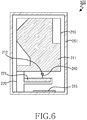
- FIG. 6 illustrates a structure of an antenna apparatus for a portable terminal according to yet another example useful for understanding the invention.
- an antenna apparatus 500 may preferably include a non-metal case frame 251 and a third metal plate 315, attached on the non-metal case frame 251, for receiving current from the main board 210 or the sub-board 220 and radiating radio waves. Also, the third metal plate 315 may be directly connected to the ground surface 221 of the sub-board 220.
- the antenna apparatus 300 shown in FIG. 4 may have a different resonant characteristic based on the thickness T of the insulating carrier 311 and a position where the first metal plate 312 is attached on the sub-board 220. Also, the antenna apparatus 400 shown in FIG. 5 or the antenna apparatus 500 shown in FIG. 6 may have a different resonant characteristic according to a position where the second metal plate 314 or the third metal plate 315 is attached.
- FIGs. 7A and FIG. 7B illustrate examples in which the ground surface of the sub-board is formed of a variety of types.
- FIG. 7C illustrates an example in which the ground surface of the main board is extended to be different from FIG. 2A and FIG. 2B .
- an antenna apparatus may have a different resonant characteristic by comprising the ground surface 221 of the sub-board 220 and the ground surface 211 of the main board 210 as a variety of types.
- a shape of the slot part 260 may differ according to a shape of the ground surface 211 of the main board 210 or a shape of the ground surface 210 of the sub-board 220.
- the thickness T of the insulating carrier 311 or 313 shown in FIG. 4 or FIG. 5 is a factor for changing a resonant characteristic.
- the antenna apparatuses of a variety of the examples and embodiments shown in FIG. 1 to FIG. 7C may have a variety of radiation elements such as the ground surface of the sub-board, the metal case frame, the first to third metal plates, the slot part installed by the combination of them, etc.
- the variety of radiation elements are matched with one another and radiate radio waves in at least one or more resonant frequency bands.
- the portable terminal may have a main antenna apparatus which radiates radio waves in a corresponding frequency band.
- the antenna apparatus according to any one of the plurality of examples and embodiments of the present invention may radiate radio waves in a resonant frequency band which is the same as or different from that of the main antenna apparatus.
- the antenna apparatus feeds power to the ground surface of the sub-board which communicates with the main board and radiates radio waves.
- the antenna apparatus according to any one of the variety of examples and embodiments of the present invention provides the first metal plate or the second metal plate, disposed on the insulating carrier fixed on the ground surface of the sub-board, which receives power from the sub-board and resonates.
- the antenna apparatus according to any one of the variety of examples and embodiments of the present invention may feed power to the metal case frame which forms the appearance of the portable terminal and may resonate.
- the antenna apparatus may feed power to the slot part installed by the combination of the ground surface of the main board, the ground surface of the sub-board, and the metal case frame and may resonate.
- the antenna apparatus may secure antenna performance in a limited space, may be easily implemented, and may reduce expenses.
Claims (14)
- Antennenvorrichtung für ein tragbares Endgerät, wobei die Vorrichtung Folgendes umfasst:eine Hauptplatine (210), die einen HF-Leistungsspeiseteil (212), der ausgelegt ist, HF-Leistung zuzuführen, und eine Hauptplatinen-Massenoberfläche (211) beinhaltet, die ausgelegt ist, die Hauptplatine (210) an Masse zu legen; undmindestens eine Nebenplatine (220), die eine Nebenplatinen-Massenoberfläche (221) aufweist und ausgelegt ist, elektrisch mit der Hauptplatine zu kommunizieren, wobei die Nebenplatinen-Massenoberfläche (221) mindestens einer Nebenplatine (220) ausgelegt ist, HF-Leistung vom HF-Leistungsspeiseteil (212) der Hauptplatine (210) zu empfangen und mit einer vorgegebenen Frequenz oder einem Bereich von Frequenzen elektromagnetischer Wellen zu resonieren, um die elektromagnetischen Wellen abzustrahlen, wobei die Antennenvorrichtung ferner einen Metallgehäuserahmen (250) zum Umhüllen der Antenne, wobei der Metallgehäuserahmen ausgelegt ist, Strom von der Hauptplatine oder der mindestens einen Nebenplatine zu empfangen und mit einer vorgegebenen Frequenz oder einem Bereich von Frequenzen elektromagnetischer Wellen zu resonieren, und einen Isolierträger (313) umfasst, der auf dem Metallgehäuserahmen (250) angeordnet ist; undeine zweite Metallplatte (314) die auf dem Isolierträger (313) angeordnet ist, die ausgelegt ist, Strom vom Metallgehäuserahmen (250) zu empfangen und mit der vorgegebenen Frequenz oder dem Bereich von Frequenzen der elektromagnetischen Wellen zu resonieren und die elektromagnetischen Wellen abzustrahlen.
- Antennenvorrichtung nach Anspruch 1, die ferner Folgendes umfasst:
eine erste Metallplatte (312), die am Isolierträger (313) angebracht ist, die ausgelegt ist, elektrisch mit der Hauptplatine zu kommunizieren, Strom von der mindestens einen Nebenplatine (220) zu empfangen und mit einer vorgegebenen Frequenz oder einem Bereich von Frequenzen elektromagnetischer Wellen zu resonieren und die elektromagnetischen Wellen abzustrahlen. - Antennenvorrichtung nach Anspruch 2, wobei die erste Metallplatte (312) elektrisch mit der Nebenplatinen-Massenoberfläche (221) jeder mindestens einen Nebenplatine (220) verbunden ist.
- Antennenvorrichtung nach Anspruch 3, wobei die erste Metallplatte (312) und die Nebenplatinen-Massenoberfläche (221) jeder mindestens einen Nebenplatine (220) elektrisch durch einen C-Clip oder einen Federkontaktstift verbunden sind.
- Antennenvorrichtung nach Anspruch 1, wobei der Metallgehäuserahmen (250) elektrisch und direkt mit dem Leistungsspeiseteil (212) der Hauptplatine gekoppelt ist oder elektrisch mit der Nebenplatinen-Massenoberfläche der mindestens einen Nebenplatine gekoppelt ist.
- Antennenvorrichtung nach Anspruch 1, wobei mindestens zwei oder mehr der Hauptplatinen-Massenoberfläche (211) der Hauptplatine (210), der Nebenplatinen-Massenoberfläche (221) der mindestens einen Nebenplatine (220) und des Metallgehäuserahmens (250) elektrisch verbunden und mit einem Schlitzteil (260) einer offenen Schleifenkontur oder einer geschlossenen Schleifenkontur ausgestattet sind, der vom Metall umgeben ist.
- Antennenvorrichtung nach Anspruch 6, die ferner eine Leistungsspeiseleitung umfasst, die ausgelegt ist, den HF-Leistungsspeiseteil (212) der Hauptplatine (210) elektrisch mit der Nebenplatinen-Massenoberfläche der mindestens einen Nebenplatine zu verbinden, wobei die Leistungsspeiseleitung auf dem Schlitzteil angeordnet ist.
- Antennenvorrichtung nach Anspruch 2, die ferner einen Metallgehäuserahmen (250) zum Umhüllen der Antennenvorrichtung umfasst, wobei der Metallgehäuserahmen (250) ausgelegt ist, Strom von der ersten Metallplatte (312) zu empfangen und mit einer vorgegebenen Frequenz oder einem Bereich von Frequenzen der elektromagnetischen Wellen zu resonieren und die elektromagnetischen Wellen abzustrahlen.
- Antennenvorrichtung nach Anspruch 1, die ferner eine dritte Metallplatte (315) umfasst, die auf einem nichtmetallischen Gehäuserahmen (251) angeordnet ist, wobei die dritte Metallplatte (315) ausgelegt ist, Strom von der Hauptplatine (210) oder der mindestens einen Nebenplatine (220) zu empfangen und mit einer vorgegebenen Frequenz oder einem Bereich von Frequenzen der elektromagnetischen Wellen zu resonieren und die elektromagnetischen Wellen abzustrahlen.
- Antennenvorrichtung nach Anspruch 1, wobei die Nebenplatinen-Massenoberfläche (221) der mindestens einen Nebenplatine (220) von der Hauptplatinen-Massenoberfläche (211) der Hauptplatine (210) beabstandet ist.
- Antennenvorrichtung nach Anspruch 1, wobei die mindestens eine Nebenplatine (220) eine starrflexible Leiterplatte, Rigid Flexible, RF-Leiterplatte, umfasst.
- Antennenvorrichtung nach Anspruch 1, wobei die mindestens eine Nebenplatine (210) eine Leiterplatte, Printed Circuit Board, PCB, oder eine flexible Leiterplatte, Flexible Printed Circuit Board, FPCB, für irgendetwas von einem Mikrofon, einem Lautsprecher, einem Empfänger, einem Tastenfeld und einer Flüssigkristallanzeige, einem Liquid Crystal Display, LCD, umfasst.
- Antennenvorrichtung nach Anspruch 1, wobei die Hauptplatine (210) und die mindestens eine Nebenplatine (220) auf einer dielektrischen Platte installiert sind.
- Endgerät, das die Antennenvorrichtung nach Anspruch 1-13 umfasst.
Applications Claiming Priority (1)
| Application Number | Priority Date | Filing Date | Title |
|---|---|---|---|
| KR1020100102263A KR101606145B1 (ko) | 2010-10-20 | 2010-10-20 | 휴대용 단말기의 안테나 장치 |
Publications (3)
| Publication Number | Publication Date |
|---|---|
| EP2458676A2 EP2458676A2 (de) | 2012-05-30 |
| EP2458676A3 EP2458676A3 (de) | 2014-01-22 |
| EP2458676B1 true EP2458676B1 (de) | 2019-03-27 |
Family
ID=44905526
Family Applications (1)
| Application Number | Title | Priority Date | Filing Date |
|---|---|---|---|
| EP11185867.6A Active EP2458676B1 (de) | 2010-10-20 | 2011-10-20 | Antennenvorrichtung für ein tragbares Endgerät |
Country Status (4)
| Country | Link |
|---|---|
| US (2) | US9065168B2 (de) |
| EP (1) | EP2458676B1 (de) |
| KR (1) | KR101606145B1 (de) |
| CN (1) | CN102544702B (de) |
Families Citing this family (17)
| Publication number | Priority date | Publication date | Assignee | Title |
|---|---|---|---|---|
| KR101606145B1 (ko) * | 2010-10-20 | 2016-03-24 | 삼성전자주식회사 | 휴대용 단말기의 안테나 장치 |
| JP6041522B2 (ja) * | 2012-04-18 | 2016-12-07 | キヤノン株式会社 | 情報処理装置、情報処理装置の制御方法、プログラム及び記憶媒体 |
| KR101977082B1 (ko) * | 2012-09-11 | 2019-05-10 | 엘지전자 주식회사 | 이동 단말기 |
| US9716307B2 (en) | 2012-11-08 | 2017-07-25 | Htc Corporation | Mobile device and antenna structure |
| TWI511381B (zh) * | 2013-10-09 | 2015-12-01 | Wistron Corp | 天線 |
| CN103682570B (zh) * | 2013-12-16 | 2016-10-05 | 联想(北京)有限公司 | 一种天线及电子设备 |
| CN103811864B (zh) * | 2014-01-25 | 2016-08-17 | 惠州硕贝德无线科技股份有限公司 | 一种金属边框双频耦合天线 |
| TWI557990B (zh) * | 2014-04-16 | 2016-11-11 | Mobile communication device | |
| TWM495681U (zh) * | 2014-08-15 | 2015-02-11 | Wistron Neweb Corp | 無線通訊裝置 |
| KR102288451B1 (ko) | 2015-02-02 | 2021-08-10 | 삼성전자주식회사 | 안테나 및 이를 구비한 전자 장치 |
| WO2016154851A1 (zh) * | 2015-03-30 | 2016-10-06 | 华为技术有限公司 | 一种终端 |
| CN105206918A (zh) * | 2015-08-28 | 2015-12-30 | 宇龙计算机通信科技(深圳)有限公司 | 一种移动终端的天线装置及移动终端 |
| WO2017142550A1 (en) * | 2016-02-19 | 2017-08-24 | Hewlett-Packard Development Company, L.P. | Integrated antenna |
| CN108206329A (zh) * | 2017-10-17 | 2018-06-26 | 中兴通讯股份有限公司 | 一种终端 |
| EP3741001A1 (de) | 2018-03-20 | 2020-11-25 | Huawei Technologies Co., Ltd. | Antennenverlängerung und elektronische vorrichtung mit antennenverlängerung |
| CN108987943B (zh) * | 2018-07-24 | 2021-04-06 | 维沃移动通信有限公司 | 一种毫米波无线终端设备 |
| CN110336112B (zh) * | 2019-05-09 | 2021-06-22 | 天通凯美微电子有限公司 | 天线馈电单元、调谐单元与显示屏组件结合的电子设备 |
Family Cites Families (18)
| Publication number | Priority date | Publication date | Assignee | Title |
|---|---|---|---|---|
| US5561437A (en) | 1994-09-15 | 1996-10-01 | Motorola, Inc. | Two position fold-over dipole antenna |
| JP2003060422A (ja) | 2001-08-09 | 2003-02-28 | Matsushita Electric Ind Co Ltd | ディスプレイ−アンテナ一体型構造体、通信装置 |
| US6867736B2 (en) * | 2002-11-08 | 2005-03-15 | Motorola, Inc. | Multi-band antennas |
| CN1989652B (zh) * | 2004-06-28 | 2013-03-13 | 脉冲芬兰有限公司 | 天线部件 |
| TWM284084U (en) * | 2004-12-28 | 2005-12-21 | Shiu Juo Gang | Antenna structure |
| KR100713513B1 (ko) | 2005-08-10 | 2007-04-30 | 삼성전자주식회사 | 휴대용 단말기의 안테나 장치 |
| KR100846343B1 (ko) | 2006-10-27 | 2008-07-15 | 삼성전자주식회사 | 휴대용 무선단말기의 내장형 안테나 장치 |
| US7688267B2 (en) | 2006-11-06 | 2010-03-30 | Apple Inc. | Broadband antenna with coupled feed for handheld electronic devices |
| JP2008124797A (ja) | 2006-11-13 | 2008-05-29 | Fujitsu Ltd | Gnd共有アンテナ |
| EP2095464A4 (de) * | 2006-11-16 | 2012-10-24 | Galtronics Ltd | Kompakte antenne |
| KR100856310B1 (ko) | 2007-02-28 | 2008-09-03 | 삼성전기주식회사 | 이동통신 단말기 |
| US7612725B2 (en) | 2007-06-21 | 2009-11-03 | Apple Inc. | Antennas for handheld electronic devices with conductive bezels |
| CA2699680C (en) * | 2007-10-08 | 2016-06-07 | Sensormatic Electronics, LLC | Rfid patch antenna with coplanar reference ground and floating grounds |
| US7551142B1 (en) * | 2007-12-13 | 2009-06-23 | Apple Inc. | Hybrid antennas with directly fed antenna slots for handheld electronic devices |
| US8106836B2 (en) | 2008-04-11 | 2012-01-31 | Apple Inc. | Hybrid antennas for electronic devices |
| US8102319B2 (en) | 2008-04-11 | 2012-01-24 | Apple Inc. | Hybrid antennas for electronic devices |
| KR101044994B1 (ko) * | 2008-06-20 | 2011-06-29 | 삼성전자주식회사 | 휴대 단말기의 안테나 장치 |
| KR101606145B1 (ko) * | 2010-10-20 | 2016-03-24 | 삼성전자주식회사 | 휴대용 단말기의 안테나 장치 |
-
2010
- 2010-10-20 KR KR1020100102263A patent/KR101606145B1/ko active IP Right Grant
-
2011
- 2011-10-18 US US13/275,701 patent/US9065168B2/en active Active
- 2011-10-19 CN CN201110319461.1A patent/CN102544702B/zh active Active
- 2011-10-20 EP EP11185867.6A patent/EP2458676B1/de active Active
-
2015
- 2015-05-29 US US14/725,433 patent/US9692108B2/en active Active
Non-Patent Citations (1)
| Title |
|---|
| None * |
Also Published As
| Publication number | Publication date |
|---|---|
| US9065168B2 (en) | 2015-06-23 |
| CN102544702B (zh) | 2015-08-12 |
| US20150263414A1 (en) | 2015-09-17 |
| KR101606145B1 (ko) | 2016-03-24 |
| EP2458676A3 (de) | 2014-01-22 |
| US9692108B2 (en) | 2017-06-27 |
| EP2458676A2 (de) | 2012-05-30 |
| KR20120040817A (ko) | 2012-04-30 |
| US20120098709A1 (en) | 2012-04-26 |
| CN102544702A (zh) | 2012-07-04 |
Similar Documents
| Publication | Publication Date | Title |
|---|---|---|
| EP2458676B1 (de) | Antennenvorrichtung für ein tragbares Endgerät | |
| CN208597073U (zh) | 电子设备 | |
| US9502750B2 (en) | Electronic device with reduced emitted radiation during loaded antenna operating conditions | |
| US9917346B2 (en) | Chassis-excited antenna apparatus and methods | |
| CN102709684B (zh) | 具有包绕的基底的多元件天线结构 | |
| US7688267B2 (en) | Broadband antenna with coupled feed for handheld electronic devices | |
| US9099774B2 (en) | Antenna | |
| US20190081396A1 (en) | Electronic Device Antennas Having Split Return Paths | |
| JP5996808B2 (ja) | 電子デバイスのためのマルチレイヤ3次元アンテナキャリア構成 | |
| US11114748B2 (en) | Flexible printed circuit structures for electronic device antennas | |
| GB2567938A (en) | Electronic devices having shared antenna structures and split return paths | |
| US9680212B2 (en) | Capacitive grounding methods and apparatus for mobile devices | |
| US7317901B2 (en) | Slotted multiple band antenna | |
| JP2002064601A (ja) | 移動電話装置及びその内蔵アンテナ | |
| US11853016B2 (en) | Electronic device wide band antennas | |
| EP2824764B1 (de) | Antennenvorrichtung und elektronische Vorrichtung mit der Antennenvorrichtung | |
| KR101305283B1 (ko) | 안테나 장치를 구비하는 휴대 단말기 | |
| US20100245203A1 (en) | Multiband antenna | |
| CN215342969U (zh) | 天线装置及电子设备 | |
| JP4133928B2 (ja) | アンテナおよびそれを用いた無線通信機 | |
| JP4885821B2 (ja) | アンテナ装置および移動体無線通信機 |
Legal Events
| Date | Code | Title | Description |
|---|---|---|---|
| PUAI | Public reference made under article 153(3) epc to a published international application that has entered the european phase |
Free format text: ORIGINAL CODE: 0009012 |
|
| AK | Designated contracting states |
Kind code of ref document: A2 Designated state(s): AL AT BE BG CH CY CZ DE DK EE ES FI FR GB GR HR HU IE IS IT LI LT LU LV MC MK MT NL NO PL PT RO RS SE SI SK SM TR |
|
| AX | Request for extension of the european patent |
Extension state: BA ME |
|
| RAP1 | Party data changed (applicant data changed or rights of an application transferred) |
Owner name: SAMSUNG ELECTRONICS CO., LTD. |
|
| PUAL | Search report despatched |
Free format text: ORIGINAL CODE: 0009013 |
|
| AK | Designated contracting states |
Kind code of ref document: A3 Designated state(s): AL AT BE BG CH CY CZ DE DK EE ES FI FR GB GR HR HU IE IS IT LI LT LU LV MC MK MT NL NO PL PT RO RS SE SI SK SM TR |
|
| AX | Request for extension of the european patent |
Extension state: BA ME |
|
| RIC1 | Information provided on ipc code assigned before grant |
Ipc: H01Q 1/48 20060101ALI20131219BHEP Ipc: H01Q 5/00 20060101ALI20131219BHEP Ipc: H01Q 9/04 20060101ALI20131219BHEP Ipc: H01Q 1/24 20060101AFI20131219BHEP Ipc: H01Q 1/38 20060101ALI20131219BHEP |
|
| 17P | Request for examination filed |
Effective date: 20140714 |
|
| RBV | Designated contracting states (corrected) |
Designated state(s): AL AT BE BG CH CY CZ DE DK EE ES FI FR GB GR HR HU IE IS IT LI LT LU LV MC MK MT NL NO PL PT RO RS SE SI SK SM TR |
|
| STAA | Information on the status of an ep patent application or granted ep patent |
Free format text: STATUS: EXAMINATION IS IN PROGRESS |
|
| 17Q | First examination report despatched |
Effective date: 20171213 |
|
| GRAP | Despatch of communication of intention to grant a patent |
Free format text: ORIGINAL CODE: EPIDOSNIGR1 |
|
| STAA | Information on the status of an ep patent application or granted ep patent |
Free format text: STATUS: GRANT OF PATENT IS INTENDED |
|
| INTG | Intention to grant announced |
Effective date: 20181108 |
|
| RIN1 | Information on inventor provided before grant (corrected) |
Inventor name: LIM, JAE-HO Inventor name: KIM, SUNG-CHEOL Inventor name: LEE, KYUNG-JONG Inventor name: LEE, JAE-HO Inventor name: CHUN, JAE-BONG Inventor name: KIM, AUSTIN |
|
| GRAS | Grant fee paid |
Free format text: ORIGINAL CODE: EPIDOSNIGR3 |
|
| GRAA | (expected) grant |
Free format text: ORIGINAL CODE: 0009210 |
|
| STAA | Information on the status of an ep patent application or granted ep patent |
Free format text: STATUS: THE PATENT HAS BEEN GRANTED |
|
| AK | Designated contracting states |
Kind code of ref document: B1 Designated state(s): AL AT BE BG CH CY CZ DE DK EE ES FI FR GB GR HR HU IE IS IT LI LT LU LV MC MK MT NL NO PL PT RO RS SE SI SK SM TR |
|
| REG | Reference to a national code |
Ref country code: GB Ref legal event code: FG4D |
|
| REG | Reference to a national code |
Ref country code: CH Ref legal event code: EP |
|
| REG | Reference to a national code |
Ref country code: AT Ref legal event code: REF Ref document number: 1114134 Country of ref document: AT Kind code of ref document: T Effective date: 20190415 |
|
| REG | Reference to a national code |
Ref country code: IE Ref legal event code: FG4D |
|
| REG | Reference to a national code |
Ref country code: DE Ref legal event code: R096 Ref document number: 602011057473 Country of ref document: DE |
|
| REG | Reference to a national code |
Ref country code: NL Ref legal event code: FP |
|
| PG25 | Lapsed in a contracting state [announced via postgrant information from national office to epo] |
Ref country code: LT Free format text: LAPSE BECAUSE OF FAILURE TO SUBMIT A TRANSLATION OF THE DESCRIPTION OR TO PAY THE FEE WITHIN THE PRESCRIBED TIME-LIMIT Effective date: 20190327 Ref country code: NO Free format text: LAPSE BECAUSE OF FAILURE TO SUBMIT A TRANSLATION OF THE DESCRIPTION OR TO PAY THE FEE WITHIN THE PRESCRIBED TIME-LIMIT Effective date: 20190627 Ref country code: FI Free format text: LAPSE BECAUSE OF FAILURE TO SUBMIT A TRANSLATION OF THE DESCRIPTION OR TO PAY THE FEE WITHIN THE PRESCRIBED TIME-LIMIT Effective date: 20190327 Ref country code: SE Free format text: LAPSE BECAUSE OF FAILURE TO SUBMIT A TRANSLATION OF THE DESCRIPTION OR TO PAY THE FEE WITHIN THE PRESCRIBED TIME-LIMIT Effective date: 20190327 |
|
| PG25 | Lapsed in a contracting state [announced via postgrant information from national office to epo] |
Ref country code: HR Free format text: LAPSE BECAUSE OF FAILURE TO SUBMIT A TRANSLATION OF THE DESCRIPTION OR TO PAY THE FEE WITHIN THE PRESCRIBED TIME-LIMIT Effective date: 20190327 Ref country code: RS Free format text: LAPSE BECAUSE OF FAILURE TO SUBMIT A TRANSLATION OF THE DESCRIPTION OR TO PAY THE FEE WITHIN THE PRESCRIBED TIME-LIMIT Effective date: 20190327 Ref country code: GR Free format text: LAPSE BECAUSE OF FAILURE TO SUBMIT A TRANSLATION OF THE DESCRIPTION OR TO PAY THE FEE WITHIN THE PRESCRIBED TIME-LIMIT Effective date: 20190628 Ref country code: BG Free format text: LAPSE BECAUSE OF FAILURE TO SUBMIT A TRANSLATION OF THE DESCRIPTION OR TO PAY THE FEE WITHIN THE PRESCRIBED TIME-LIMIT Effective date: 20190627 Ref country code: LV Free format text: LAPSE BECAUSE OF FAILURE TO SUBMIT A TRANSLATION OF THE DESCRIPTION OR TO PAY THE FEE WITHIN THE PRESCRIBED TIME-LIMIT Effective date: 20190327 |
|
| REG | Reference to a national code |
Ref country code: AT Ref legal event code: MK05 Ref document number: 1114134 Country of ref document: AT Kind code of ref document: T Effective date: 20190327 |
|
| PG25 | Lapsed in a contracting state [announced via postgrant information from national office to epo] |
Ref country code: EE Free format text: LAPSE BECAUSE OF FAILURE TO SUBMIT A TRANSLATION OF THE DESCRIPTION OR TO PAY THE FEE WITHIN THE PRESCRIBED TIME-LIMIT Effective date: 20190327 Ref country code: SK Free format text: LAPSE BECAUSE OF FAILURE TO SUBMIT A TRANSLATION OF THE DESCRIPTION OR TO PAY THE FEE WITHIN THE PRESCRIBED TIME-LIMIT Effective date: 20190327 Ref country code: ES Free format text: LAPSE BECAUSE OF FAILURE TO SUBMIT A TRANSLATION OF THE DESCRIPTION OR TO PAY THE FEE WITHIN THE PRESCRIBED TIME-LIMIT Effective date: 20190327 Ref country code: CZ Free format text: LAPSE BECAUSE OF FAILURE TO SUBMIT A TRANSLATION OF THE DESCRIPTION OR TO PAY THE FEE WITHIN THE PRESCRIBED TIME-LIMIT Effective date: 20190327 Ref country code: PT Free format text: LAPSE BECAUSE OF FAILURE TO SUBMIT A TRANSLATION OF THE DESCRIPTION OR TO PAY THE FEE WITHIN THE PRESCRIBED TIME-LIMIT Effective date: 20190727 Ref country code: AL Free format text: LAPSE BECAUSE OF FAILURE TO SUBMIT A TRANSLATION OF THE DESCRIPTION OR TO PAY THE FEE WITHIN THE PRESCRIBED TIME-LIMIT Effective date: 20190327 Ref country code: RO Free format text: LAPSE BECAUSE OF FAILURE TO SUBMIT A TRANSLATION OF THE DESCRIPTION OR TO PAY THE FEE WITHIN THE PRESCRIBED TIME-LIMIT Effective date: 20190327 Ref country code: IT Free format text: LAPSE BECAUSE OF FAILURE TO SUBMIT A TRANSLATION OF THE DESCRIPTION OR TO PAY THE FEE WITHIN THE PRESCRIBED TIME-LIMIT Effective date: 20190327 |
|
| PG25 | Lapsed in a contracting state [announced via postgrant information from national office to epo] |
Ref country code: PL Free format text: LAPSE BECAUSE OF FAILURE TO SUBMIT A TRANSLATION OF THE DESCRIPTION OR TO PAY THE FEE WITHIN THE PRESCRIBED TIME-LIMIT Effective date: 20190327 Ref country code: SM Free format text: LAPSE BECAUSE OF FAILURE TO SUBMIT A TRANSLATION OF THE DESCRIPTION OR TO PAY THE FEE WITHIN THE PRESCRIBED TIME-LIMIT Effective date: 20190327 |
|
| PG25 | Lapsed in a contracting state [announced via postgrant information from national office to epo] |
Ref country code: AT Free format text: LAPSE BECAUSE OF FAILURE TO SUBMIT A TRANSLATION OF THE DESCRIPTION OR TO PAY THE FEE WITHIN THE PRESCRIBED TIME-LIMIT Effective date: 20190327 Ref country code: IS Free format text: LAPSE BECAUSE OF FAILURE TO SUBMIT A TRANSLATION OF THE DESCRIPTION OR TO PAY THE FEE WITHIN THE PRESCRIBED TIME-LIMIT Effective date: 20190727 |
|
| REG | Reference to a national code |
Ref country code: DE Ref legal event code: R097 Ref document number: 602011057473 Country of ref document: DE |
|
| PG25 | Lapsed in a contracting state [announced via postgrant information from national office to epo] |
Ref country code: DK Free format text: LAPSE BECAUSE OF FAILURE TO SUBMIT A TRANSLATION OF THE DESCRIPTION OR TO PAY THE FEE WITHIN THE PRESCRIBED TIME-LIMIT Effective date: 20190327 |
|
| PLBE | No opposition filed within time limit |
Free format text: ORIGINAL CODE: 0009261 |
|
| STAA | Information on the status of an ep patent application or granted ep patent |
Free format text: STATUS: NO OPPOSITION FILED WITHIN TIME LIMIT |
|
| PG25 | Lapsed in a contracting state [announced via postgrant information from national office to epo] |
Ref country code: SI Free format text: LAPSE BECAUSE OF FAILURE TO SUBMIT A TRANSLATION OF THE DESCRIPTION OR TO PAY THE FEE WITHIN THE PRESCRIBED TIME-LIMIT Effective date: 20190327 |
|
| 26N | No opposition filed |
Effective date: 20200103 |
|
| PG25 | Lapsed in a contracting state [announced via postgrant information from national office to epo] |
Ref country code: TR Free format text: LAPSE BECAUSE OF FAILURE TO SUBMIT A TRANSLATION OF THE DESCRIPTION OR TO PAY THE FEE WITHIN THE PRESCRIBED TIME-LIMIT Effective date: 20190327 |
|
| PG25 | Lapsed in a contracting state [announced via postgrant information from national office to epo] |
Ref country code: MC Free format text: LAPSE BECAUSE OF FAILURE TO SUBMIT A TRANSLATION OF THE DESCRIPTION OR TO PAY THE FEE WITHIN THE PRESCRIBED TIME-LIMIT Effective date: 20190327 |
|
| REG | Reference to a national code |
Ref country code: CH Ref legal event code: PL |
|
| PG25 | Lapsed in a contracting state [announced via postgrant information from national office to epo] |
Ref country code: LU Free format text: LAPSE BECAUSE OF NON-PAYMENT OF DUE FEES Effective date: 20191020 Ref country code: LI Free format text: LAPSE BECAUSE OF NON-PAYMENT OF DUE FEES Effective date: 20191031 Ref country code: CH Free format text: LAPSE BECAUSE OF NON-PAYMENT OF DUE FEES Effective date: 20191031 |
|
| REG | Reference to a national code |
Ref country code: BE Ref legal event code: MM Effective date: 20191031 |
|
| PG25 | Lapsed in a contracting state [announced via postgrant information from national office to epo] |
Ref country code: BE Free format text: LAPSE BECAUSE OF NON-PAYMENT OF DUE FEES Effective date: 20191031 |
|
| PG25 | Lapsed in a contracting state [announced via postgrant information from national office to epo] |
Ref country code: IE Free format text: LAPSE BECAUSE OF NON-PAYMENT OF DUE FEES Effective date: 20191020 Ref country code: FR Free format text: LAPSE BECAUSE OF NON-PAYMENT OF DUE FEES Effective date: 20191031 |
|
| PG25 | Lapsed in a contracting state [announced via postgrant information from national office to epo] |
Ref country code: CY Free format text: LAPSE BECAUSE OF FAILURE TO SUBMIT A TRANSLATION OF THE DESCRIPTION OR TO PAY THE FEE WITHIN THE PRESCRIBED TIME-LIMIT Effective date: 20190327 |
|
| PG25 | Lapsed in a contracting state [announced via postgrant information from national office to epo] |
Ref country code: MT Free format text: LAPSE BECAUSE OF FAILURE TO SUBMIT A TRANSLATION OF THE DESCRIPTION OR TO PAY THE FEE WITHIN THE PRESCRIBED TIME-LIMIT Effective date: 20190327 Ref country code: HU Free format text: LAPSE BECAUSE OF FAILURE TO SUBMIT A TRANSLATION OF THE DESCRIPTION OR TO PAY THE FEE WITHIN THE PRESCRIBED TIME-LIMIT; INVALID AB INITIO Effective date: 20111020 |
|
| PG25 | Lapsed in a contracting state [announced via postgrant information from national office to epo] |
Ref country code: MK Free format text: LAPSE BECAUSE OF FAILURE TO SUBMIT A TRANSLATION OF THE DESCRIPTION OR TO PAY THE FEE WITHIN THE PRESCRIBED TIME-LIMIT Effective date: 20190327 |
|
| PGFP | Annual fee paid to national office [announced via postgrant information from national office to epo] |
Ref country code: NL Payment date: 20230921 Year of fee payment: 13 Ref country code: GB Payment date: 20230920 Year of fee payment: 13 |
|
| PGFP | Annual fee paid to national office [announced via postgrant information from national office to epo] |
Ref country code: DE Payment date: 20230920 Year of fee payment: 13 |