EP2458621B1 - Procédé de réalisation amélioré d'un motif à partir du transfert par espaceurs latéraux - Google Patents
Procédé de réalisation amélioré d'un motif à partir du transfert par espaceurs latéraux Download PDFInfo
- Publication number
- EP2458621B1 EP2458621B1 EP11354071.0A EP11354071A EP2458621B1 EP 2458621 B1 EP2458621 B1 EP 2458621B1 EP 11354071 A EP11354071 A EP 11354071A EP 2458621 B1 EP2458621 B1 EP 2458621B1
- Authority
- EP
- European Patent Office
- Prior art keywords
- etching mask
- etching
- layer
- covering layer
- covering
- Prior art date
- Legal status (The legal status is an assumption and is not a legal conclusion. Google has not performed a legal analysis and makes no representation as to the accuracy of the status listed.)
- Not-in-force
Links
- 125000006850 spacer group Chemical group 0.000 title claims description 39
- 238000000034 method Methods 0.000 title claims description 27
- 238000005530 etching Methods 0.000 claims description 177
- 239000000463 material Substances 0.000 claims description 127
- 230000000873 masking effect Effects 0.000 claims description 26
- 239000000758 substrate Substances 0.000 claims description 11
- 230000015572 biosynthetic process Effects 0.000 claims description 5
- 238000004519 manufacturing process Methods 0.000 claims description 4
- 239000010410 layer Substances 0.000 description 70
- 238000000206 photolithography Methods 0.000 description 14
- 230000036961 partial effect Effects 0.000 description 7
- 238000000151 deposition Methods 0.000 description 5
- 230000000694 effects Effects 0.000 description 4
- 238000002310 reflectometry Methods 0.000 description 4
- 230000007423 decrease Effects 0.000 description 3
- 238000001459 lithography Methods 0.000 description 3
- 230000003071 parasitic effect Effects 0.000 description 3
- 239000011347 resin Substances 0.000 description 3
- 229920005989 resin Polymers 0.000 description 3
- 229910052581 Si3N4 Inorganic materials 0.000 description 2
- VYPSYNLAJGMNEJ-UHFFFAOYSA-N Silicium dioxide Chemical compound O=[Si]=O VYPSYNLAJGMNEJ-UHFFFAOYSA-N 0.000 description 2
- 230000008021 deposition Effects 0.000 description 2
- 239000012777 electrically insulating material Substances 0.000 description 2
- 238000001020 plasma etching Methods 0.000 description 2
- 230000002829 reductive effect Effects 0.000 description 2
- 239000004065 semiconductor Substances 0.000 description 2
- HQVNEWCFYHHQES-UHFFFAOYSA-N silicon nitride Chemical compound N12[Si]34N5[Si]62N3[Si]51N64 HQVNEWCFYHHQES-UHFFFAOYSA-N 0.000 description 2
- 229910052814 silicon oxide Inorganic materials 0.000 description 2
- 238000012876 topography Methods 0.000 description 2
- ATJFFYVFTNAWJD-UHFFFAOYSA-N Tin Chemical compound [Sn] ATJFFYVFTNAWJD-UHFFFAOYSA-N 0.000 description 1
- 150000001721 carbon Chemical class 0.000 description 1
- 239000003575 carbonaceous material Substances 0.000 description 1
- 230000015556 catabolic process Effects 0.000 description 1
- 238000005229 chemical vapour deposition Methods 0.000 description 1
- 239000011248 coating agent Substances 0.000 description 1
- 238000000576 coating method Methods 0.000 description 1
- 239000000470 constituent Substances 0.000 description 1
- 238000006731 degradation reaction Methods 0.000 description 1
- 230000001627 detrimental effect Effects 0.000 description 1
- 238000009499 grossing Methods 0.000 description 1
- 238000011065 in-situ storage Methods 0.000 description 1
- 230000000670 limiting effect Effects 0.000 description 1
- 239000000203 mixture Substances 0.000 description 1
- 230000003287 optical effect Effects 0.000 description 1
- 230000035515 penetration Effects 0.000 description 1
- 239000011241 protective layer Substances 0.000 description 1
- 238000011084 recovery Methods 0.000 description 1
- 229910052710 silicon Inorganic materials 0.000 description 1
- 239000010703 silicon Substances 0.000 description 1
- 239000007787 solid Substances 0.000 description 1
- 238000004528 spin coating Methods 0.000 description 1
- 239000000126 substance Substances 0.000 description 1
Images


Classifications
-
- H—ELECTRICITY
- H01—ELECTRIC ELEMENTS
- H01L—SEMICONDUCTOR DEVICES NOT COVERED BY CLASS H10
- H01L21/00—Processes or apparatus adapted for the manufacture or treatment of semiconductor or solid state devices or of parts thereof
- H01L21/02—Manufacture or treatment of semiconductor devices or of parts thereof
- H01L21/027—Making masks on semiconductor bodies for further photolithographic processing not provided for in group H01L21/18 or H01L21/34
- H01L21/0271—Making masks on semiconductor bodies for further photolithographic processing not provided for in group H01L21/18 or H01L21/34 comprising organic layers
- H01L21/0273—Making masks on semiconductor bodies for further photolithographic processing not provided for in group H01L21/18 or H01L21/34 comprising organic layers characterised by the treatment of photoresist layers
- H01L21/0274—Photolithographic processes
-
- H—ELECTRICITY
- H01—ELECTRIC ELEMENTS
- H01L—SEMICONDUCTOR DEVICES NOT COVERED BY CLASS H10
- H01L21/00—Processes or apparatus adapted for the manufacture or treatment of semiconductor or solid state devices or of parts thereof
- H01L21/02—Manufacture or treatment of semiconductor devices or of parts thereof
- H01L21/027—Making masks on semiconductor bodies for further photolithographic processing not provided for in group H01L21/18 or H01L21/34
- H01L21/033—Making masks on semiconductor bodies for further photolithographic processing not provided for in group H01L21/18 or H01L21/34 comprising inorganic layers
- H01L21/0334—Making masks on semiconductor bodies for further photolithographic processing not provided for in group H01L21/18 or H01L21/34 comprising inorganic layers characterised by their size, orientation, disposition, behaviour, shape, in horizontal or vertical plane
- H01L21/0337—Making masks on semiconductor bodies for further photolithographic processing not provided for in group H01L21/18 or H01L21/34 comprising inorganic layers characterised by their size, orientation, disposition, behaviour, shape, in horizontal or vertical plane characterised by the process involved to create the mask, e.g. lift-off masks, sidewalls, or to modify the mask, e.g. pre-treatment, post-treatment
-
- G—PHYSICS
- G03—PHOTOGRAPHY; CINEMATOGRAPHY; ANALOGOUS TECHNIQUES USING WAVES OTHER THAN OPTICAL WAVES; ELECTROGRAPHY; HOLOGRAPHY
- G03F—PHOTOMECHANICAL PRODUCTION OF TEXTURED OR PATTERNED SURFACES, e.g. FOR PRINTING, FOR PROCESSING OF SEMICONDUCTOR DEVICES; MATERIALS THEREFOR; ORIGINALS THEREFOR; APPARATUS SPECIALLY ADAPTED THEREFOR
- G03F1/00—Originals for photomechanical production of textured or patterned surfaces, e.g., masks, photo-masks, reticles; Mask blanks or pellicles therefor; Containers specially adapted therefor; Preparation thereof
- G03F1/68—Preparation processes not covered by groups G03F1/20 - G03F1/50
- G03F1/80—Etching
Definitions
- the invention relates to a method of producing a pattern of first material.
- An alternative development path is to define the width and / or the length of the desired pattern by means of a step of depositing a material of masking. In this way, at least one of the lateral dimensions of the pattern is not defined by photolithography, but by means of the deposition of a predefined thickness of masking material.
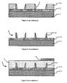
- a substrate 1 is covered by a layer of first material 2, itself covered by a covering layer 3.
- An etching mask 4 is formed, by any suitable technique, on the covering layer 3.
- the covering layer 3 is etched, for example by plasma, through the etching mask 4 in order to reproduce in the latter the pattern of the etching mask 4.
- the etching chemistry is chosen to be selective with respect to the etching mask and with respect to the first material 2 so as to eliminate part of the covering layer 3 without damaging the first material 2, nor modifying the pattern of the etching mask 4.
- a loss of selectivity vis-à-vis the first material 2 results in particular degradation of physico-chemical properties and a decrease in the thickness of the first material which is detrimental to the successful completion of subsequent steps.
- the etching chemistry is chosen as anisotropic as possible in order to faithfully reproduce the pattern of the etching mask 4 in the covering layer 3.
- This etching step forms a pattern of covering material 3 defined from the drawing of the etching mask 4.
- the first etching mask 4 is eliminated.
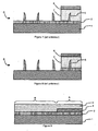
- a masking material 5 is deposited and etched to form one or more lateral spacers.
- the masking material 5 is suitably deposited and etched anisotropically to locate it on the side walls of the cover material pattern 3.
- the thickness of deposited material defines one of the dimensions of the pattern of masking material 5. This dimension is reduced during the plasma etching step.
- the photolithography step defines the position of the patterns and the step of forming the lateral spacers defines at least one of the lateral dimensions of these patterns.
- the etching of the masking material 5 uses a chemistry which is highly anisotropic and selective with respect to the first material 2 and the covering material 3.
- the covering material 3 is removed and the spacers form a second etching mask 6.
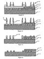
- the second etching mask 6, obtained by the lateral spacer transfer technique is covered by a second covering material 7.
- a third etching mask 8 is formed on the second covering material 7.
- the second covering material 7 is etched by means of the third etching mask 8 until it reaches the second etching mask 6 and the first material 2.
- the first material 2 is then etched by means of the second etching mask 6 (the spacers of masking material 5) and the third etching mask 8 as illustrated in FIG. figure 8 to form a pattern of first material.
- the pattern of the first material pattern 2 corresponds to the combination of the drawings of the second etching mask 6 and the third etching mask 8.
- a substrate 1 comprises a support which is covered by a layer of first material 2.
- the layer of first material 2 is covered by a first etching mask 4 and a covering layer 3.
- the support is, for example, a substrate of semiconductor material with active components covered by one or more protective layers.
- the support may also be formed by an electrically conductive or electrically insulating material on the surface of which patterns are to be formed.
- the main face of the support is formed by one or more layers of electrically insulating material.
- the main face of the support is covered by the layer of first material 2.
- the first material 2 may be insulating or electrically conductive.
- the first material is electrically conductive, for example TiN, BN, TaN, AlN with an advantageous thickness of between 10 and 50 nm.
- the first etching mask 4 is formed on the first material layer 2.
- the first etching mask 4 defines a main zone A and a secondary zone B on the first material 2.
- the main zone A is covered directly by the first mask of engraving 4 and the secondary zone B is covered directly by the covering layer 3.
- the drawing of the etching mask 4 is any, it is defined according to the desired patterns.
- the first etching mask 4 is disposed between the first material layer 2 and the covering layer 3 and prevents the direct contact between the first material 2 and the covering layer 3 in the main zone A.
- the first etching mask 4 is for example a silicon oxide, a silicon nitride, a mixture or a stack of these.
- the first etching mask may be formed in another material as long as the nature of its constituents is compatible with its position between the first material 2 and the covering layer 3.
- the cover layer 3 has antireflection properties to facilitate the formation of a second etching mask 6 thereafter.
- the covering material 3 is a carbonaceous material deposited by chemical vapor deposition or by spin coating.
- the material used is represented by the formula CxHy which reflects a more or less hydrogenated carbon type material.
- a second etching mask 6 is formed on the covering layer 3.
- the second etching mask 6 also defines a main zone C and a secondary zone D on the covering layer 3.
- the main zone C is covered by the second mask engraving 6 and the secondary zone D is discovered, it is left free.
- the drawing of the second etching mask 6 is arbitrary, it is defined according to the desired patterns, with respect to the drawing of the first etching mask 4.
- the first 4 and second 6 etching masks are separated by the covering layer 3.
- the second etching mask 6 is, for example, a photosensitive resin or a material of different nature.
- the second etch mask 6 is silicon oxide, silicon nitride, a stack of silicon or another material.
- the second etching mask 6 is not a resin, it is advantageous to define its shape by means of a photolithography step followed by an etching step.
- the second etching mask 6 is also called a hard mask.
- the covering material 3 is etched, by any suitable technique, by means of the second etching mask 6.
- the etching of the covering layer 3 is partial.
- the part of the covering material 3 left free is partially etched so as to form a projecting pattern in the covering layer 3.
- This partial etching is represented by zones of different thicknesses. In the main zone C covered by the second etching mask 6, the thickness is unchanged and represents a thick zone.
- the cover layer 3 has been partially removed and this corresponds to a thin zone of the layer 3.
- the pattern of the second etching mask 6 has been reproduced in the cover layer 3 through the second etching mask 6 and the outline of the drawing is formed by lateral walls which are vertical or substantially vertical and which connect the thin zone to the thick area.
- the etching of the covering layer 3 being carried out on only a part of the thickness of the covering material, the height of the side wall is less than the thickness of the covering layer 3.
- the covering layer 3 is thus structured so as to form zones with different thicknesses, which results in the presence of protruding patterns in the layer of covering material on a continuous film of covering material 3.
- the first material 2 and the first etching mask 4 are completely covered by the covering layer 3.
- the etching is performed by plasma by imposing the etching time or by controlling the etching thickness by in situ reflectometry.
- a masking material 5 is then deposited conformably or as uniformly as possible on the assembly and covers the covering layer 3 and the second etching mask 6.
- the thickness deposited on the vertical walls is identical to the thickness deposited on the horizontal walls.
- the masking material is etched by any suitable technique, preferably with anisotropic plasma etching, in order to form lateral spacers. The etching makes it possible to locate the masking material 5 on the vertical walls defined in the covering layer 3. In this way, after the etching step, the masking material 5 forms lateral spacers which cover the side walls of the coating material. recovery 3.
- the second etching mask 6 is removed in order to leave the covering material 3 and the masking material spacers 5 on the surface.
- the masking material spacers 5 form a third etching mask 8.
- the drawing of the third mask etching 8 is defined in part by the drawing of the second etching mask 6 which imposes the position of the lateral spacers.
- the pattern of the third etching mask 8 is also defined from the thickness of the masking material deposited and the thickness etched to define the lateral spacers.
- the covering layer 3 is etched by means of the third etching mask 8 so as to form a pattern protruding into the covering layer 3.
- the etching is complete so as to reach the first material 2 or the first etching mask 4.
- the covering material 3 is eliminated under the zones initially covered by the second etching mask 6 as well as in the second zone D at the places not covered by the lateral spacers.
- the patterns of covering material 3 are formed in the thin zone, their thickness has been defined during the partial etching of the covering material 3.
- the patterns of covering material 3 reproduce the pattern of the third etching mask 8.
- This embodiment is particularly advantageous because it offers greater flexibility in the definition of the third etching mask 8.
- a deposit is never perfectly consistent and etching is never perfectly anisotropic. It emerges that, in the prior art, the shape of the lateral spacers is limited by the technological possibilities of the equipment or by the constraints in minimum thicknesses imposed by other technological steps. In the prior art, the thickness of the covering layer gives the height of the lateral spacers.
- the difference in thickness between the thin zone and the thick zone and the thickness of the second etching mask 6 imposes the height of the lateral spacers. It is then possible to modulate the depth of penetration in the covering material 3 in order to obtain a deposit of the masking material 5 which makes it possible to obtain a compliant or as compliant deposit as possible. Similarly, this flexibility in the height of the lateral spacers provides more efficient etching processes. The completion of the partial etching of the covering material 3 makes it possible to obtain additional degrees of freedom in the production of the lateral spacers to the desired shape.
- the thickness of Cover material 3 can thus be chosen independently to minimize reflectivity during lithography.
- the covering material 3 As the first etching mask 4 is covered by the covering material 3, there is no parasitic step between the first etching mask 4 and the first material 2. As a result, parasitic side spacers are not formed at the same time. level of this walk.
- the partial etching of the covering material 3 makes it possible to erase the surface inequalities present before the deposition of the covering material, for example, a surface topography on the substrate 1 and / or on the layer of first material 2 as well as the topography of the surface between the first material 2 and the first etching mask 4.
- the thickness of the covering layer 3 is chosen so as to limit the effect of the layers and the lower patterns during the step of defining the second etching mask 6. It is then possible to use a covering layer 3 thick enough to hide the effect of the lower layers. The thickness of the cover layer 3 is no longer a constraint because it is etched twice.
- the first partial etching makes it possible to define the third etching mask 7 under the best conditions.
- the second complete engraving allows to define the final mask to be used to engrave the first material 2.
- the first etching mask 4 is made conventionally, that is to say by a technique other than by transfer of lateral spacers, it is possible to obtain patterns having a large width. It is then easy to align the second etching mask 6 with respect to the first etching mask.
- the first etching mask 4 is obtained with the technique of transfer of lateral spacers which imposes small patterns that make it difficult to align the following photolithographic levels.
- the second etching mask that defines the most critical dimensions is made on a strong topology, which requires the use of smoothing material. This strong topology induces disparities of reflectivity for the lithography which hinder the obtaining of the sought resolution.
- This topology also induces local temperature differences, depending on the density of the underlying patterns, which change the size of the patterns in the end. Moreover, the patterns transferred in the second covering material 7 ( figure 7 ) have a high form factor (ratio between width and height), which leads to mechanical resistance problems for these reasons.
- the first etching mask 4 which defines the most critical dimensions is made on a surface without topology and has a smaller thickness than the etching mask formed by the lateral spacer transfer technique.
- the effect of the first etching mask 4 on the definition of the second etching mask 6 is reduced.
- the first etching mask 4 and the pattern formed in the covering layer form a fourth etching mask which is used to etch the first material 2.
- the drawing of the fourth etching mask corresponds to the addition of the solid areas of the first etching mask 4 and the third etching mask 8. Differences may exist if the etching of the covering material comprises an isotropic component or if a shrinking step decreases the size of the reasons or makes disappear the smaller reasons.
- the first material pattern 2 is formed through the fourth etching mask and thus through the first etching mask 4 and the cover material pattern 3.
- the second etching mask 6 is removed before depositing the masking material 5 and forming the lateral spacers.
- the height of the lateral spacers is defined from the depression in the covering material 3 which leaves the same room for maneuver as in the previous embodiment.
- the second etching mask 6 is eliminated after the production of the lateral spacers, it is necessary to ensure an etching selectivity not only between the material of the second etching mask 6 and the covering material 3, but also between the material of the second mask of FIG. etching 6 and the masking material 5.
- the lateral spacers forming the third etching mask 8 are formed in the same manner as before and the third etching mask 8 is used as before to etch the covering material 3.
- the final structure is identical to that illustrated in FIG. figure 16 of the previous embodiment.
- the etching of the covering material 3 is carried out by means of a selective etching of the covering material 3 with respect to the third etching mask 8.
- the third etching mask 8 is eliminated selectively with respect to the 3.
- the masking material 5 is selectively removed from the cover material 3 to form the lateral spacers.
- the covering material 3 is selectively removed from the masking material 5 to reproduce the pattern of the third etching mask 8.
- each etching step is performed with a limited number of materials. On the surface of the substrate, only the material to be removed and the material to be preserved are present. There is no, as in the prior art, a material to be removed in the presence of two materials to keep. The result is greater freedom of choice in the processes that can be used to perform etching and / or more robust etching processes.
- the first etching mask 4 is covered by the covering material 3.
- the integral covering of the first etching mask 4 by the covering material makes it possible to limit the number of visible material during the etching step and thus facilitate the development of etching chemistry.
- the first etching mask 4 is obtained directly by means of a photolithography step followed by an etching step.
- the drawing of the first engraving mask 4 comes directly from the drawing of a resin mask.
- This direct definition from the drawing defined by photolithography makes it possible to easily form zones of different sizes, advantageously areas having dimensions significantly greater than those defined in the third etching mask 8 by the spacers.
- a large alignment pattern is formed, for example, at least a few microns in the first etching mask 4. This large pattern allows easy alignment of the photolithography level of the second etching mask 6 relative to the one that defined the first etching mask 4.
- the photolithographic levels are reversed, the etching mask obtained by transfer of the lateral spacers is formed before the etching mask obtained by photolithography.
- This arrangement of lithography steps makes it necessary to achieve more difficult alignment by means of areas with large densities of small patterns. This method therefore makes it possible to obtain a better alignment of the two photolithographic levels used and / or a more robust alignment method.
- the first etching mask 4 is formed in a conventional manner.
- the substrate 1 is provided with the first material layer 2 covered by an additional masking layer 9 and an additional etching mask 10.
- An additional covering layer (not shown) may be used to reduce the influence of the substrate 1 during the formation of the additional etching mask 10.
- the additional covering layer and the additional masking layer 9 are etched and the masking layer 9 forms the first etching mask 4.
- the additional etching mask 10 and the additional covering layer are removed to leave on the surface only the first etching mask 4.
- the first etching mask 4 may be obtained indirectly from the drawing of the photolithography level used, for example using the transfer by lateral spacers.
- the second etching mask 6 When the second etching mask 6 is formed by photolithography on the covering material 3 this imposes certain constraints, in particular, in the choice of the covering material 3 and in the usable thickness. These constraints are intended to facilitate the photolithography step by reducing the reflectivity problems and the optical influence of the lower layers. These constraints have the effect of increasing the thickness of the covering layer 3 in order to facilitate the formation of the second etching mask 4. As indicated above, the covering layer 3 must also allow the definition of the lateral spacers. which limits the range of accessible materials and / or usable thickness ranges to obtain a method which is in accordance with the imposed relief.
- the photolithography step is performed on a certain thickness of covering material 3. This thickness is chosen to facilitate the photolithography step.
- the layer of covering material 3 is then etched to form a thick zone and a thin zone and this difference in thickness is used to facilitate the definition of the lateral spacers with the chosen dimensional ratio.
- the definition of the spacers is facilitated because a wider choice of materials is accessible, difficulties in obtaining a compliant deposit being partly erased by the flexibility in the choice of the difference in thickness between the thin zone and the thick zone.
Landscapes
- Engineering & Computer Science (AREA)
- General Physics & Mathematics (AREA)
- Physics & Mathematics (AREA)
- Manufacturing & Machinery (AREA)
- Condensed Matter Physics & Semiconductors (AREA)
- Computer Hardware Design (AREA)
- Microelectronics & Electronic Packaging (AREA)
- Power Engineering (AREA)
- Inorganic Chemistry (AREA)
- Chemical & Material Sciences (AREA)
- Drying Of Semiconductors (AREA)
- Internal Circuitry In Semiconductor Integrated Circuit Devices (AREA)
- Semiconductor Memories (AREA)
Applications Claiming Priority (1)
| Application Number | Priority Date | Filing Date | Title |
|---|---|---|---|
| FR1004655A FR2968122B1 (fr) | 2010-11-30 | 2010-11-30 | Procédé de réalisation amélioré d'un motif a partir du transfert par espaceurs latéraux |
Publications (2)
| Publication Number | Publication Date |
|---|---|
| EP2458621A1 EP2458621A1 (fr) | 2012-05-30 |
| EP2458621B1 true EP2458621B1 (fr) | 2015-02-25 |
Family
ID=44276342
Family Applications (1)
| Application Number | Title | Priority Date | Filing Date |
|---|---|---|---|
| EP11354071.0A Not-in-force EP2458621B1 (fr) | 2010-11-30 | 2011-11-29 | Procédé de réalisation amélioré d'un motif à partir du transfert par espaceurs latéraux |
Country Status (7)
Families Citing this family (9)
| Publication number | Priority date | Publication date | Assignee | Title |
|---|---|---|---|---|
| FR2990794B1 (fr) * | 2012-05-16 | 2016-11-18 | Commissariat Energie Atomique | Procede de realisation d'un substrat muni de zones actives variees et de transistors planaires et tridimensionnels |
| US8735296B2 (en) * | 2012-07-18 | 2014-05-27 | International Business Machines Corporation | Method of simultaneously forming multiple structures having different critical dimensions using sidewall transfer |
| US8716133B2 (en) * | 2012-08-23 | 2014-05-06 | International Business Machines Corporation | Three photomask sidewall image transfer method |
| US9040371B2 (en) | 2013-08-07 | 2015-05-26 | International Business Machines Corporation | Integration of dense and variable pitch fin structures |
| US9293345B2 (en) | 2013-08-16 | 2016-03-22 | Globalfoundries Inc. | Sidewall image transfer with a spin-on hardmask |
| US9064901B1 (en) | 2013-12-23 | 2015-06-23 | International Business Machines Corporation | Fin density control of multigate devices through sidewall image transfer processes |
| US9252243B2 (en) | 2014-02-07 | 2016-02-02 | International Business Machines Corporation | Gate structure integration scheme for fin field effect transistors |
| CN106373880B (zh) * | 2015-07-22 | 2021-05-25 | 联华电子股份有限公司 | 半导体元件及其形成方法 |
| CN112768351B (zh) * | 2019-11-06 | 2022-06-10 | 长鑫存储技术有限公司 | 一种图形形成方法 |
Family Cites Families (5)
| Publication number | Priority date | Publication date | Assignee | Title |
|---|---|---|---|---|
| US7151040B2 (en) * | 2004-08-31 | 2006-12-19 | Micron Technology, Inc. | Methods for increasing photo alignment margins |
| US7615445B2 (en) * | 2006-09-21 | 2009-11-10 | Sandisk Corporation | Methods of reducing coupling between floating gates in nonvolatile memory |
| US7479429B2 (en) * | 2007-01-31 | 2009-01-20 | Freescale Semiconductor, Inc. | Split game memory cell method |
| KR100966976B1 (ko) * | 2007-12-28 | 2010-06-30 | 주식회사 하이닉스반도체 | 반도체 소자의 제조 방법 |
| US9330934B2 (en) * | 2009-05-18 | 2016-05-03 | Micron Technology, Inc. | Methods of forming patterns on substrates |
-
2010
- 2010-11-30 FR FR1004655A patent/FR2968122B1/fr not_active Expired - Fee Related
-
2011
- 2011-11-21 US US13/301,251 patent/US8669188B2/en active Active
- 2011-11-22 SG SG2011086600A patent/SG181266A1/en unknown
- 2011-11-28 TW TW100143525A patent/TWI529777B/zh not_active IP Right Cessation
- 2011-11-29 EP EP11354071.0A patent/EP2458621B1/fr not_active Not-in-force
- 2011-11-29 KR KR1020110126366A patent/KR101881594B1/ko not_active Expired - Fee Related
- 2011-11-29 JP JP2011260794A patent/JP5959833B2/ja not_active Expired - Fee Related
Also Published As
| Publication number | Publication date |
|---|---|
| EP2458621A1 (fr) | 2012-05-30 |
| US8669188B2 (en) | 2014-03-11 |
| TWI529777B (en) | 2016-04-11 |
| KR101881594B1 (ko) | 2018-07-24 |
| FR2968122B1 (fr) | 2012-12-07 |
| US20120132616A1 (en) | 2012-05-31 |
| KR20120059426A (ko) | 2012-06-08 |
| SG181266A1 (en) | 2012-06-28 |
| TW201222627A (en) | 2012-06-01 |
| JP5959833B2 (ja) | 2016-08-02 |
| JP2012138570A (ja) | 2012-07-19 |
| FR2968122A1 (fr) | 2012-06-01 |
Similar Documents
| Publication | Publication Date | Title |
|---|---|---|
| EP2458621B1 (fr) | Procédé de réalisation amélioré d'un motif à partir du transfert par espaceurs latéraux | |
| EP2577395B1 (fr) | Procede de lithographie a dedoublement de pas | |
| EP2999001B1 (fr) | Réalisation d'espaceurs au niveau de flancs d'une grille de transistor | |
| FR3043837A1 (fr) | Procede de realisation de transistor a nanofil semi-conducteur et comprenant une grille et des espaceurs auto-alignes | |
| FR3046290B1 (fr) | Methode de realisation d'espaceurs a faible permittivite | |
| FR2672731A1 (fr) | Procede d'oxydation localisee enterree d'un substrat de silicium et circuit integre correspondant. | |
| EP2769249A1 (fr) | Procede de realisation d'un dispositif optique refractif ou diffractif | |
| EP3506336B1 (fr) | Procédé de gravure d'une couche diélectrique tridimensionnelle | |
| WO2017093359A1 (fr) | Procédé permettant d'obtenir sur un substrat cristallin une couche semi-polaire de nitrure | |
| EP3246948B1 (fr) | Procédé de réalisation sur un même substrat de transistors présentant des caractéristiques différentes | |
| FR3057991A1 (fr) | Procede de formation d’un guide d’assemblage fonctionnalise | |
| EP2577723A1 (fr) | Procede de lithographie pour la realisation de reseaux de conducteurs relies par des vias | |
| EP2339616B1 (fr) | Procédé de réalisation simplifié d'un substrat hybride | |
| FR3009430A1 (fr) | Procede de realisation d'un motif dans un circuit integre et circuit integre correspondant | |
| EP3729491A1 (fr) | Procédé de formation d'une structure de guidage chimique sur un substrat et procédé de chémo-épitaxie | |
| FR2963477A1 (fr) | Procédé de réalisation amélioré d'un motif a partir du transfert par espaceurs latéraux | |
| FR2718287A1 (fr) | Procédé de fabrication d'un transistor à effet de champ à grille isolée, en particulier de longueur de canal réduite, et transistor correspondant. | |
| EP1071122B1 (fr) | Procédé de correction des effets topographiques sur substrat en micro electronique | |
| FR3091002A1 (fr) | Procédé de gravure d’une couche diélectrique tridimensionnelle | |
| FR2948495A1 (fr) | Composants a contact électrique traversant et procédé de fabrication ainsi que système comportant de tels composants | |
| FR2734403A1 (fr) | Isolement plan dans des circuits integres | |
| EP2479793A1 (fr) | Procédé de fabrication d'un dispositif à effet de champ avec une faible capacité de jonction | |
| EP3889683A1 (fr) | Procédé de réalisation d'une zone d'individualisation d'un circuit intégré | |
| EP2665086A1 (fr) | Procédé de réalisation d'un substrat muni de zones actives variées et de transistors planaires et tridimensionnels | |
| EP3667734B1 (fr) | Procédé de fabrication de composants microélectroniques |
Legal Events
| Date | Code | Title | Description |
|---|---|---|---|
| PUAI | Public reference made under article 153(3) epc to a published international application that has entered the european phase |
Free format text: ORIGINAL CODE: 0009012 |
|
| AK | Designated contracting states |
Kind code of ref document: A1 Designated state(s): AL AT BE BG CH CY CZ DE DK EE ES FI FR GB GR HR HU IE IS IT LI LT LU LV MC MK MT NL NO PL PT RO RS SE SI SK SM TR |
|
| AX | Request for extension of the european patent |
Extension state: BA ME |
|
| 17P | Request for examination filed |
Effective date: 20121128 |
|
| GRAP | Despatch of communication of intention to grant a patent |
Free format text: ORIGINAL CODE: EPIDOSNIGR1 |
|
| INTG | Intention to grant announced |
Effective date: 20140422 |
|
| GRAJ | Information related to disapproval of communication of intention to grant by the applicant or resumption of examination proceedings by the epo deleted |
Free format text: ORIGINAL CODE: EPIDOSDIGR1 |
|
| GRAP | Despatch of communication of intention to grant a patent |
Free format text: ORIGINAL CODE: EPIDOSNIGR1 |
|
| INTG | Intention to grant announced |
Effective date: 20140526 |
|
| GRAP | Despatch of communication of intention to grant a patent |
Free format text: ORIGINAL CODE: EPIDOSNIGR1 |
|
| INTG | Intention to grant announced |
Effective date: 20141031 |
|
| GRAS | Grant fee paid |
Free format text: ORIGINAL CODE: EPIDOSNIGR3 |
|
| GRAF | Information related to payment of grant fee modified |
Free format text: ORIGINAL CODE: EPIDOSCIGR3 |
|
| GRAA | (expected) grant |
Free format text: ORIGINAL CODE: 0009210 |
|
| AK | Designated contracting states |
Kind code of ref document: B1 Designated state(s): AL AT BE BG CH CY CZ DE DK EE ES FI FR GB GR HR HU IE IS IT LI LT LU LV MC MK MT NL NO PL PT RO RS SE SI SK SM TR |
|
| REG | Reference to a national code |
Ref country code: GB Ref legal event code: FG4D Free format text: NOT ENGLISH |
|
| REG | Reference to a national code |
Ref country code: CH Ref legal event code: EP |
|
| REG | Reference to a national code |
Ref country code: IE Ref legal event code: FG4D Free format text: LANGUAGE OF EP DOCUMENT: FRENCH |
|
| REG | Reference to a national code |
Ref country code: DE Ref legal event code: R096 Ref document number: 602011013956 Country of ref document: DE Effective date: 20150409 |
|
| REG | Reference to a national code |
Ref country code: AT Ref legal event code: REF Ref document number: 712623 Country of ref document: AT Kind code of ref document: T Effective date: 20150415 |
|
| REG | Reference to a national code |
Ref country code: NL Ref legal event code: VDEP Effective date: 20150225 |
|
| REG | Reference to a national code |
Ref country code: AT Ref legal event code: MK05 Ref document number: 712623 Country of ref document: AT Kind code of ref document: T Effective date: 20150225 |
|
| REG | Reference to a national code |
Ref country code: LT Ref legal event code: MG4D |
|
| PG25 | Lapsed in a contracting state [announced via postgrant information from national office to epo] |
Ref country code: HR Free format text: LAPSE BECAUSE OF FAILURE TO SUBMIT A TRANSLATION OF THE DESCRIPTION OR TO PAY THE FEE WITHIN THE PRESCRIBED TIME-LIMIT Effective date: 20150225 Ref country code: LT Free format text: LAPSE BECAUSE OF FAILURE TO SUBMIT A TRANSLATION OF THE DESCRIPTION OR TO PAY THE FEE WITHIN THE PRESCRIBED TIME-LIMIT Effective date: 20150225 Ref country code: FI Free format text: LAPSE BECAUSE OF FAILURE TO SUBMIT A TRANSLATION OF THE DESCRIPTION OR TO PAY THE FEE WITHIN THE PRESCRIBED TIME-LIMIT Effective date: 20150225 Ref country code: ES Free format text: LAPSE BECAUSE OF FAILURE TO SUBMIT A TRANSLATION OF THE DESCRIPTION OR TO PAY THE FEE WITHIN THE PRESCRIBED TIME-LIMIT Effective date: 20150225 Ref country code: NO Free format text: LAPSE BECAUSE OF FAILURE TO SUBMIT A TRANSLATION OF THE DESCRIPTION OR TO PAY THE FEE WITHIN THE PRESCRIBED TIME-LIMIT Effective date: 20150525 Ref country code: SE Free format text: LAPSE BECAUSE OF FAILURE TO SUBMIT A TRANSLATION OF THE DESCRIPTION OR TO PAY THE FEE WITHIN THE PRESCRIBED TIME-LIMIT Effective date: 20150225 |
|
| PG25 | Lapsed in a contracting state [announced via postgrant information from national office to epo] |
Ref country code: LV Free format text: LAPSE BECAUSE OF FAILURE TO SUBMIT A TRANSLATION OF THE DESCRIPTION OR TO PAY THE FEE WITHIN THE PRESCRIBED TIME-LIMIT Effective date: 20150225 Ref country code: IS Free format text: LAPSE BECAUSE OF FAILURE TO SUBMIT A TRANSLATION OF THE DESCRIPTION OR TO PAY THE FEE WITHIN THE PRESCRIBED TIME-LIMIT Effective date: 20150625 Ref country code: GR Free format text: LAPSE BECAUSE OF FAILURE TO SUBMIT A TRANSLATION OF THE DESCRIPTION OR TO PAY THE FEE WITHIN THE PRESCRIBED TIME-LIMIT Effective date: 20150526 Ref country code: AT Free format text: LAPSE BECAUSE OF FAILURE TO SUBMIT A TRANSLATION OF THE DESCRIPTION OR TO PAY THE FEE WITHIN THE PRESCRIBED TIME-LIMIT Effective date: 20150225 Ref country code: RS Free format text: LAPSE BECAUSE OF FAILURE TO SUBMIT A TRANSLATION OF THE DESCRIPTION OR TO PAY THE FEE WITHIN THE PRESCRIBED TIME-LIMIT Effective date: 20150225 |
|
| PG25 | Lapsed in a contracting state [announced via postgrant information from national office to epo] |
Ref country code: NL Free format text: LAPSE BECAUSE OF FAILURE TO SUBMIT A TRANSLATION OF THE DESCRIPTION OR TO PAY THE FEE WITHIN THE PRESCRIBED TIME-LIMIT Effective date: 20150225 |
|
| PG25 | Lapsed in a contracting state [announced via postgrant information from national office to epo] |
Ref country code: DK Free format text: LAPSE BECAUSE OF FAILURE TO SUBMIT A TRANSLATION OF THE DESCRIPTION OR TO PAY THE FEE WITHIN THE PRESCRIBED TIME-LIMIT Effective date: 20150225 Ref country code: EE Free format text: LAPSE BECAUSE OF FAILURE TO SUBMIT A TRANSLATION OF THE DESCRIPTION OR TO PAY THE FEE WITHIN THE PRESCRIBED TIME-LIMIT Effective date: 20150225 Ref country code: CZ Free format text: LAPSE BECAUSE OF FAILURE TO SUBMIT A TRANSLATION OF THE DESCRIPTION OR TO PAY THE FEE WITHIN THE PRESCRIBED TIME-LIMIT Effective date: 20150225 Ref country code: SK Free format text: LAPSE BECAUSE OF FAILURE TO SUBMIT A TRANSLATION OF THE DESCRIPTION OR TO PAY THE FEE WITHIN THE PRESCRIBED TIME-LIMIT Effective date: 20150225 Ref country code: RO Free format text: LAPSE BECAUSE OF FAILURE TO SUBMIT A TRANSLATION OF THE DESCRIPTION OR TO PAY THE FEE WITHIN THE PRESCRIBED TIME-LIMIT Effective date: 20150225 |
|
| REG | Reference to a national code |
Ref country code: DE Ref legal event code: R097 Ref document number: 602011013956 Country of ref document: DE |
|
| PG25 | Lapsed in a contracting state [announced via postgrant information from national office to epo] |
Ref country code: PL Free format text: LAPSE BECAUSE OF FAILURE TO SUBMIT A TRANSLATION OF THE DESCRIPTION OR TO PAY THE FEE WITHIN THE PRESCRIBED TIME-LIMIT Effective date: 20150225 |
|
| REG | Reference to a national code |
Ref country code: FR Ref legal event code: PLFP Year of fee payment: 5 |
|
| PG25 | Lapsed in a contracting state [announced via postgrant information from national office to epo] |
Ref country code: IT Free format text: LAPSE BECAUSE OF FAILURE TO SUBMIT A TRANSLATION OF THE DESCRIPTION OR TO PAY THE FEE WITHIN THE PRESCRIBED TIME-LIMIT Effective date: 20150225 |
|
| PLBE | No opposition filed within time limit |
Free format text: ORIGINAL CODE: 0009261 |
|
| STAA | Information on the status of an ep patent application or granted ep patent |
Free format text: STATUS: NO OPPOSITION FILED WITHIN TIME LIMIT |
|
| 26N | No opposition filed |
Effective date: 20151126 |
|
| PG25 | Lapsed in a contracting state [announced via postgrant information from national office to epo] |
Ref country code: SI Free format text: LAPSE BECAUSE OF FAILURE TO SUBMIT A TRANSLATION OF THE DESCRIPTION OR TO PAY THE FEE WITHIN THE PRESCRIBED TIME-LIMIT Effective date: 20150225 |
|
| PG25 | Lapsed in a contracting state [announced via postgrant information from national office to epo] |
Ref country code: LU Free format text: LAPSE BECAUSE OF FAILURE TO SUBMIT A TRANSLATION OF THE DESCRIPTION OR TO PAY THE FEE WITHIN THE PRESCRIBED TIME-LIMIT Effective date: 20151129 Ref country code: MC Free format text: LAPSE BECAUSE OF FAILURE TO SUBMIT A TRANSLATION OF THE DESCRIPTION OR TO PAY THE FEE WITHIN THE PRESCRIBED TIME-LIMIT Effective date: 20150225 |
|
| REG | Reference to a national code |
Ref country code: CH Ref legal event code: PL |
|
| PG25 | Lapsed in a contracting state [announced via postgrant information from national office to epo] |
Ref country code: CH Free format text: LAPSE BECAUSE OF NON-PAYMENT OF DUE FEES Effective date: 20151130 Ref country code: LI Free format text: LAPSE BECAUSE OF NON-PAYMENT OF DUE FEES Effective date: 20151130 |
|
| REG | Reference to a national code |
Ref country code: IE Ref legal event code: MM4A |
|
| PG25 | Lapsed in a contracting state [announced via postgrant information from national office to epo] |
Ref country code: IE Free format text: LAPSE BECAUSE OF NON-PAYMENT OF DUE FEES Effective date: 20151129 |
|
| REG | Reference to a national code |
Ref country code: FR Ref legal event code: PLFP Year of fee payment: 6 |
|
| PGFP | Annual fee paid to national office [announced via postgrant information from national office to epo] |
Ref country code: GB Payment date: 20161121 Year of fee payment: 6 |
|
| PG25 | Lapsed in a contracting state [announced via postgrant information from national office to epo] |
Ref country code: HU Free format text: LAPSE BECAUSE OF FAILURE TO SUBMIT A TRANSLATION OF THE DESCRIPTION OR TO PAY THE FEE WITHIN THE PRESCRIBED TIME-LIMIT; INVALID AB INITIO Effective date: 20111129 Ref country code: BG Free format text: LAPSE BECAUSE OF FAILURE TO SUBMIT A TRANSLATION OF THE DESCRIPTION OR TO PAY THE FEE WITHIN THE PRESCRIBED TIME-LIMIT Effective date: 20150225 Ref country code: SM Free format text: LAPSE BECAUSE OF FAILURE TO SUBMIT A TRANSLATION OF THE DESCRIPTION OR TO PAY THE FEE WITHIN THE PRESCRIBED TIME-LIMIT Effective date: 20150225 |
|
| PG25 | Lapsed in a contracting state [announced via postgrant information from national office to epo] |
Ref country code: CY Free format text: LAPSE BECAUSE OF FAILURE TO SUBMIT A TRANSLATION OF THE DESCRIPTION OR TO PAY THE FEE WITHIN THE PRESCRIBED TIME-LIMIT Effective date: 20150225 |
|
| PG25 | Lapsed in a contracting state [announced via postgrant information from national office to epo] |
Ref country code: BE Free format text: LAPSE BECAUSE OF NON-PAYMENT OF DUE FEES Effective date: 20151130 |
|
| PG25 | Lapsed in a contracting state [announced via postgrant information from national office to epo] |
Ref country code: MT Free format text: LAPSE BECAUSE OF FAILURE TO SUBMIT A TRANSLATION OF THE DESCRIPTION OR TO PAY THE FEE WITHIN THE PRESCRIBED TIME-LIMIT Effective date: 20150225 Ref country code: TR Free format text: LAPSE BECAUSE OF FAILURE TO SUBMIT A TRANSLATION OF THE DESCRIPTION OR TO PAY THE FEE WITHIN THE PRESCRIBED TIME-LIMIT Effective date: 20150225 |
|
| REG | Reference to a national code |
Ref country code: FR Ref legal event code: PLFP Year of fee payment: 7 |
|
| PG25 | Lapsed in a contracting state [announced via postgrant information from national office to epo] |
Ref country code: PT Free format text: LAPSE BECAUSE OF FAILURE TO SUBMIT A TRANSLATION OF THE DESCRIPTION OR TO PAY THE FEE WITHIN THE PRESCRIBED TIME-LIMIT Effective date: 20150225 Ref country code: MK Free format text: LAPSE BECAUSE OF FAILURE TO SUBMIT A TRANSLATION OF THE DESCRIPTION OR TO PAY THE FEE WITHIN THE PRESCRIBED TIME-LIMIT Effective date: 20150225 |
|
| GBPC | Gb: european patent ceased through non-payment of renewal fee |
Effective date: 20171129 |
|
| PG25 | Lapsed in a contracting state [announced via postgrant information from national office to epo] |
Ref country code: AL Free format text: LAPSE BECAUSE OF FAILURE TO SUBMIT A TRANSLATION OF THE DESCRIPTION OR TO PAY THE FEE WITHIN THE PRESCRIBED TIME-LIMIT Effective date: 20150225 |
|
| PG25 | Lapsed in a contracting state [announced via postgrant information from national office to epo] |
Ref country code: GB Free format text: LAPSE BECAUSE OF NON-PAYMENT OF DUE FEES Effective date: 20171129 |
|
| PGFP | Annual fee paid to national office [announced via postgrant information from national office to epo] |
Ref country code: DE Payment date: 20181112 Year of fee payment: 8 |
|
| PGFP | Annual fee paid to national office [announced via postgrant information from national office to epo] |
Ref country code: FR Payment date: 20181129 Year of fee payment: 8 |
|
| REG | Reference to a national code |
Ref country code: DE Ref legal event code: R119 Ref document number: 602011013956 Country of ref document: DE |
|
| PG25 | Lapsed in a contracting state [announced via postgrant information from national office to epo] |
Ref country code: DE Free format text: LAPSE BECAUSE OF NON-PAYMENT OF DUE FEES Effective date: 20200603 |
|
| PG25 | Lapsed in a contracting state [announced via postgrant information from national office to epo] |
Ref country code: FR Free format text: LAPSE BECAUSE OF NON-PAYMENT OF DUE FEES Effective date: 20191202 |