EP2456193B1 - Processing detector array signals using stacked readout integrated circuits - Google Patents
Processing detector array signals using stacked readout integrated circuits Download PDFInfo
- Publication number
- EP2456193B1 EP2456193B1 EP11190023.9A EP11190023A EP2456193B1 EP 2456193 B1 EP2456193 B1 EP 2456193B1 EP 11190023 A EP11190023 A EP 11190023A EP 2456193 B1 EP2456193 B1 EP 2456193B1
- Authority
- EP
- European Patent Office
- Prior art keywords
- roic
- current
- detected light
- time period
- switch
- Prior art date
- Legal status (The legal status is an assumption and is not a legal conclusion. Google has not performed a legal analysis and makes no representation as to the accuracy of the status listed.)
- Active
Links
Images

Classifications
-
- G—PHYSICS
- G01—MEASURING; TESTING
- G01J—MEASUREMENT OF INTENSITY, VELOCITY, SPECTRAL CONTENT, POLARISATION, PHASE OR PULSE CHARACTERISTICS OF INFRARED, VISIBLE OR ULTRAVIOLET LIGHT; COLORIMETRY; RADIATION PYROMETRY
- G01J1/00—Photometry, e.g. photographic exposure meter
- G01J1/42—Photometry, e.g. photographic exposure meter using electric radiation detectors
- G01J1/44—Electric circuits
- G01J1/46—Electric circuits using a capacitor
-
- G—PHYSICS
- G01—MEASURING; TESTING
- G01J—MEASUREMENT OF INTENSITY, VELOCITY, SPECTRAL CONTENT, POLARISATION, PHASE OR PULSE CHARACTERISTICS OF INFRARED, VISIBLE OR ULTRAVIOLET LIGHT; COLORIMETRY; RADIATION PYROMETRY
- G01J3/00—Spectrometry; Spectrophotometry; Monochromators; Measuring colours
- G01J3/28—Investigating the spectrum
- G01J3/2803—Investigating the spectrum using photoelectric array detector
-
- G—PHYSICS
- G01—MEASURING; TESTING
- G01J—MEASUREMENT OF INTENSITY, VELOCITY, SPECTRAL CONTENT, POLARISATION, PHASE OR PULSE CHARACTERISTICS OF INFRARED, VISIBLE OR ULTRAVIOLET LIGHT; COLORIMETRY; RADIATION PYROMETRY
- G01J3/00—Spectrometry; Spectrophotometry; Monochromators; Measuring colours
- G01J3/28—Investigating the spectrum
- G01J3/30—Measuring the intensity of spectral lines directly on the spectrum itself
- G01J3/36—Investigating two or more bands of a spectrum by separate detectors
-
- H—ELECTRICITY
- H04—ELECTRIC COMMUNICATION TECHNIQUE
- H04N—PICTORIAL COMMUNICATION, e.g. TELEVISION
- H04N25/00—Circuitry of solid-state image sensors [SSIS]; Control thereof
- H04N25/50—Control of the SSIS exposure
- H04N25/57—Control of the dynamic range
- H04N25/58—Control of the dynamic range involving two or more exposures
-
- H—ELECTRICITY
- H10—SEMICONDUCTOR DEVICES; ELECTRIC SOLID-STATE DEVICES NOT OTHERWISE PROVIDED FOR
- H10F—INORGANIC SEMICONDUCTOR DEVICES SENSITIVE TO INFRARED RADIATION, LIGHT, ELECTROMAGNETIC RADIATION OF SHORTER WAVELENGTH OR CORPUSCULAR RADIATION
- H10F39/00—Integrated devices, or assemblies of multiple devices, comprising at least one element covered by group H10F30/00, e.g. radiation detectors comprising photodiode arrays
- H10F39/80—Constructional details of image sensors
- H10F39/804—Containers or encapsulations
Definitions
- This invention relates generally to the field of detector arrays and more specifically to processing detector array signals using stacked readout integrated circuits.
- Detector systems may include a detector array and a read out integrated circuit (ROIC).
- a detector array may include detector pixels that detect light and generate currents in response to detecting the light.
- An ROIC may include unit cells that process the currents generated by the detector pixels.
- US patent application US2009/0173883A1 describes a multi-band focal plane array architecture operative to detect multiple spectral images.
- the multi-band focal plane array architecture has an integrated readout circuit, a plurality of first detectors integrated in the readout circuit and a plurality of second detectors deposited on the readout circuit.
- US patent application US 2004/0004707A1 describes a single dual mode monolithic focal plane array having an active sensor and a passive sensing capability that is switched from one mode to the other by switching the bias across the cells of the array from a passive IR mode to an active LADAR mode.
- a cell of the array comprises a read out integrated circuit (ROIC) which may include a pair of silicon layers, one embodying an active read-out and the other embodying a passive read out.
- a conductive layer 106 is in contact with N/N+ regions of the cell and descends downwardly to a pad at which read out circuitry is used to probe the array for results of detection in either one of two modes.
- ROIC read out integrated circuit
- US patent US 7,492,399 B1 describes a High Dynamic Range Dual Mode input 30 circuit unit cell for use with an infrared radiation detector.
- the readout circuit unit cell includes a plurality of transistors, switches, and capacitances that are controllably coupled together to form, in a first mode of operation below an illumination level threshold, a CTIA input circuit, and to form, in a second mode of operation above the illumination level threshold, a lower gain SFD input circuit.
- US patent application US 2002/000819A1 describes a photo detector device capable of simultaneously detecting two or more selected wavelengths of light on a pixel-registered basis.
- the device has detector layers of selected semiconductor materials of one micron or less in thickness interspersed with contact layers, each detector layer having a different light absorption to wavelength response curve. All contact layers, including detector bias voltages, have electrical contacts on the backside of the pixel for discrete pixel connection to mating connections on a suitable ROIC substrate.
- an apparatus comprises a first readout integrated circuit (ROIC), a second ROIC, and a dual band detector array.
- the first ROIC comprises first unit cells.
- the second ROIC is disposed outwardly from the first ROIC and comprises a second unit cells.
- Electrically conductive vias are disposed through the second ROIC and at least into the first ROIC.
- the detector array is disposed outwardly from the second ROIC.
- the detector array is configured to detect high dynamic range infrared light and comprises detector pixels. Each detector pixel is configured to generate a current in response to detecting light and send the current to a via.
- a via is configured to send the signal to a second unit cell and a first unit cell.
- a method includes generating, by a detector pixel of a detector array, a current in response to detecting light.
- the detector array comprises detector pixels and is disposed outwardly from a second readout integrated circuit (ROIC).
- the current is sent by the detector pixel to a via of a plurality of electrically conductive vias disposed through the second ROIC and at least into a first ROIC.
- the signal is sent by the via to a second unit cell of the second ROIC and to a first unit cell of the first ROIC.
- the first ROIC comprises first unit cells
- the second ROIC is disposed outwardly from the first ROIC and comprises second unit cells.
- an apparatus comprises a first readout integrated circuit (ROIC), a second ROIC, a detector array, and a switch.
- the first ROIC comprises first unit cells and operates as a high flux ROIC configured to process the current to capture higher flux detected light.
- the second ROIC is disposed outwardly from the first ROIC and comprises second unit cells.
- the second ROIC operates as a low flux ROIC configured to process the current to capture lower flux detected light.
- Electrically conductive vias are disposed through the second ROIC and at least into the first ROIC.
- the detector array is disposed outwardly from the second ROIC and comprises detector pixels. Each detector pixel is configured to generate a current in response to detecting light and to send the current to a via.
- the via is configured to send the signal to a second unit cell and a first unit cell.
- the switch is coupled to the detector array and is configured, for a first time period, to send the current to the first ROIC operating as a high flux ROIC and, for a second time period, to send the current to the second ROIC operating as a low flux ROIC.
- the second time period is greater than the first time period.
- FIGURES 1 through 3 of the drawings like numerals being used for like and corresponding parts of the various drawings.
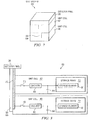
- FIGURE 1 illustrates an example of an apparatus that includes stacked ROICs configured to process detector signals.
- the ROICs may perform different operations.
- stacking the ROICs may allow for more efficient use of substrate area.
- apparatus 10 comprises a first readout integrated circuit (ROIC) 20, a second ROIC 22, a detector array 24, and an image processing system 36 coupled as shown.
- ROICs 40 and 42 comprise one or more column amplifiers 46 and 48 and buffers 30 and 32, respectively.
- Bond pads 50 and 52 provide output from ROICs 20 and 22, respectively.
- first ROIC 20 comprises first unit cells 40.
- Second ROIC 22 is disposed outwardly from first ROIC 20 and comprises second unit cells 42.
- Electrically conductive vertical interconnect accesses (vias) 50 are disposed through second ROIC 22 and at least into and perhaps through first ROIC 20.
- Detector array 24 is disposed outwardly from second ROIC 22 and comprises detector pixels 38. Each detector pixel 38 is configured to generate a current in response to detecting light and send the current to a via 50, which is configured to send the signal to a second unit cell 42 and a first unit cell 40.
- Column amplifiers 46 and 48 amplify output of unit cells 40 and 42, respectively. Bond pads 50 and 52 provide the amplified output from column amplifiers 46 and 48, respectively.
- Buffers 30 and 32 buffer output from ROICs 20 and 22, respectively.
- Image processing system 36 receives output from buffers 30 and 32 and generates image data from the output that may be used to initiate display of an image.
- each of 38, 40, and 42 may represent different functional circuits that correspond to different substrates on which complementary metal-oxide-semiconductor (CMOS) circuitry is formed.
- CMOS complementary metal-oxide-semiconductor
- the cut away view of apparatus 10 shows only one row of detector pixels 38 and unit cells 40 and 42.
- Detector array 24 and ROICs 20 and 22, however, may include any suitable number of rows and columns of detector pixels 38 and unit cells 40 and 42, respectively.
- detector array 24 comprises an array of detector pixels 38.
- a detector pixel 38 comprises a photodetector that senses and converts radiation into an analog electrical signal that may manipulated by a unit cell 40 and/or 42.
- a detector pixel 38 may detect light of any suitable radiant flux.
- a detector pixel 38 may detect light of a higher flux (for example, greater than 10 15 photons/cm 2 ⁇ sec) and/or light of a lower flux (for example, less than 10 15 photons/cm 2 ⁇ sec).
- a detector pixel 38 may detect light of any suitable wavelength band.
- wavelength bands include short wavelength infrared (IR) (SWIR) (approximately 1000 to 3000 nm), medium wavelength IR (MWIR) (approximately 3000 to 8000 nm), long wavelength IR (LWIR) (approximately 7000 to 14,000 nm), and very long wavelength IR (VLWIR) (approximately 12,000 to 30,000 nm), as well as bands above or below the IR bands.
- SWIR short wavelength infrared
- MWIR medium wavelength IR
- LWIR long wavelength IR
- VLWIR very long wavelength IR
- Detector pixels 38 may be sensitive to a common wavelength band, or may include a set of pixels 38 sensitive to one wavelength band and one or more other sets of pixels 38 sensitive to one or more other wavelength bands.
- a dual detector array may comprise a first set of pixels 38 sensitive to a first wavelength band and a second set of pixels 38 sensitive to a second wavelength band.
- the first and second wavelength bands may be any suitable wavelength bands.
- the first wavelength band may be SWIR and the second wavelength band may be MWIR.
- Detector array 24 may detect light of any suitable luminance.
- detector array 24 may detect light (such as infrared light) in a high dynamic range of luminance.
- detector array 24 may have a dynamic range with a value x, where x is an element of 60 to 90, 90 to 120, or greater than 120 decibels (dB)
- an ROIC 20 or 22 is an electrical circuit multiplexer that interfaces with detector array 24 and operates as analog dynamic range management circuitry.
- An ROIC 20 or 22 comprises an array of unit cells 40 or 42 that each bias a detector pixel 38.
- a unit cell 40 or 42 integrates charge received from a detector pixel 38 into a capacitor.
- First ROIC 20 comprises first unit cells 40
- second ROIC 22 comprises second unit cells 42.
- An example of a unit cell is described with reference to FIGURE 2 .
- ROIC 20 or 22 may be formed from a silicon-based substrate.
- CMOS circuitry may be formed outwardly from the substrate by etching, growing, and disposing layers of material.
- the array of detector pixels 38 may be hybridized to the substrate of ROIC 20 or 22.
- Certain circuits of ROIC 20 or 22 may be made monolithically with detector pixels 38 or may be formed separately from detector pixels 38.
- one ROIC may operate as a high flux sensing ROIC (or a high flux sensing low power dissipation ROIC), and the other ROIC (second or first ROIC) may operate as a low flux sensing ROIC (or a low flux sensing high power dissipation ROIC).
- first ROIC 20 may operate as a high sensing flux ROIC
- second ROIC 22 may operate as a low sensing flux ROIC.
- a high flux ROIC may be configured to process current to capture higher flux light.
- the high flux ROIC may be an ROIC that consumes less power than a low flux ROIC. Examples include direct injection (DI) unit cell.
- DI direct injection
- SFA sub-frame averaging
- a low flux ROIC may be configured to process photo current generated by lower flux light.
- the low flux ROIC may be an ROIC that consumes more power than a high flux ROIC. Examples include a capacitive transimpedance amplifier (CTIA) and a buffered direct injection (BDI) unit cell.
- CTIA capacitive transimpedance amplifier
- BDI buffered direct injection
- MFA multi-frame averaging
- first ROIC 20 may be configured to process current associated with light of a first wavelength band
- second ROIC 22 may be configured to process current associated with light of a second wavelength band that may be the same as or different from the first wavelength band.
- ROICs 20 and 22 may process any suitable wavelength bands, for example, the wavelength bands listed above.
- detector array 24 may be configured to send current to ROICs 20 and 22 by alternating between ROICs 20 and 22. For example, detector array 24 may send the current to an ROIC operating as a high flux ROIC for a first time period, and then to the other ROIC operating as a low flux ROIC for a second time period.
- the second time period may be greater than, equal to, or less than the first time period.
- the second time period (for the low flux ROIC) may be greater than the first time period (for the high flux ROIC).
- current may be sent to ROICs 20 and 22 according to a schedule that may achieve temporal alignment among frames of different wavelength bands.
- current may be sent to first ROIC 20 integrating a first wavelength band (for example, the LWIR band) and to second ROIC 22 integrating a second wavelength band (for example, the MWIR band).
- Current may be sent to first ROIC 20 for a first time period that occurs before and after a second time period during which current is sent to second ROIC 22.
- the first and second time periods may have any suitable duration, and the first time period may be greater than, equal to, or less than the second time period.
- the first time period may be approximately 1 millisecond
- the second time period may be approximately 2 to 5 milliseconds.
- ROICs 20 and 22 may process in parallel and output complete arrays of data.
- a complete array of data may refer to data that includes output from at least most or all unit cells of the ROIC.
- a complete array of data may be used to generate a frame of an image.
- apparatus 10 may output one or more first frames of data generated by first ROIC 20, and then output one or more second frames of data generated by second ROIC 22.
- first column amplifiers 46 may be configured to amplify output from first ROIC 20
- second column amplifiers 48 may be configured to amplify output from second ROIC 22.
- column amplifiers include single-ended or differential CTIA per column or voltage mode amplifier per column amplifiers.
- one or more first buffers 30 may be configured to buffer output from first ROIC 20, and one or more second buffers 32 may be configured to buffer output from second ROIC 22.
- buffers include voltage mode amplifiers such as voltage followers, single-ended, or differential amplifiers.
- image processing system 36 may receive one or more first frames of data generated by first ROIC 20 and one or more second frames of data generated by second ROIC 22. Image processing system 36 may analyze the first and second frames of data to generate an image in any suitable manner. For example, image processing system may fuse first and second frame data to yield composite frame data, and generate a frame of an image from the composite frame data.
- FIGURE 2 illustrates an example of a unit system 60.
- unit system 60 includes a unit cell 40, a unit cell 42, and a detector pixel 38.
- Via 50 electrically couples a detector pixel 38 to a unit cell 40 and/or unit cell 42 and may transport a current from detector pixel 38 to unit cell 42 and/or unit cell 40.
- via 50 may be a hole (such as an opening or aperture) with conductive material disposed within the hole. Any suitable conductive material may be used, for example, an insulating oxide material. Via 50 may be suitable via, such as a through silicon via (TSV). Via 50 may have any suitable form. For example, via 50 may have openings on opposing surfaces of a substrate, an opening on only one surface, or no opening on any surface.
- TSV through silicon via
- FIGURE 3 illustrates unit system 60 in more detail.
- unit system 60 includes detector pixel 38, unit cells 40 and 42, and via 50 coupled as shown.
- Each unit cell 40 and 42 includes a switch 70, circuitry 80, a capacitor 84, and a storage array 72.
- Storage array 72 includes storage elements 90 that store output from unit cells 40 or 42 of an ROIC 20 or 22.
- detector pixel 38 detects light and outputs a current in response to detecting light.
- Switch 70 directs the current to unit cell 40 and/or 42 through via 50.
- Unit cells 40 and 42 process the current to yield an output, which is stored at storage elements 90.
- unit cell 40 or 42 may have a capacitor 84 and circuitry 80, which may include a ramp circuit and an analog-to-digital converter (A/D).
- Capacitor 84 may have a first and an opposed second plate.
- the ramp circuit may provide a voltage ramp to the capacitor first plate.
- the capacitor second plate may receive current from detector pixel 38.
- the A/D receives analog output from the capacitor second plate and provides digital output to a storage element 90.
- a counter may be coupled in parallel to outputs of an array of unit cells, and may accumulate digital outputs from each digital inverter in a global count.
- Switch 70 resides in at least some unit cells, and may provide controlled connections to via 50.
- switch 70 may be configured to send current to ROICs 20 and 22 by alternating between ROICs 20 and 22.
- switch 70 may send the current to an ROIC operating as a high flux ROIC for a first time period, and then to the other ROIC operating as a low flux ROIC for a second time period.
- the second time period may be greater than, equal to, or less than the first time period.
- the second time period (for the low flux ROIC) may be greater than the first time period (for the high flux ROIC).
- switch 70 may send the current to an ROIC used for a first wavelength band for a first time period, and then the current to the other ROIC used for a second wavelength band for a second time period, where the second wavelength band includes larger wavelengths.
- the second time period may be greater than, equal to, or less than the first time period.
- the second time period (for the larger wavelengths) may be greater than or less than the first time period (for the smaller wavelengths).
- the first time period may be a value in the range of 1 to 100 microsecond (ps), and the second time period may be a value in the range of 1000 to 20000ps.
- Unit cell 40 or 42 may be any suitable size, for example, less than 20 microns x 20 microns (20pm x 20pm) square. Unit cell 40 or 42 may operate with any suitable frame rate, such as 30 hertz (Hz), 60 Hz, 120 Hz, or greater frame rates.
- Hz hertz
- 60 Hz 60 Hz
- 120 Hz 120 Hz
- a component of the systems and apparatuses disclosed herein may include an interface, logic, memory, and/or other suitable element.
- An interface receives input, sends output, processes the input and/or output, and/or performs other suitable operation.
- An interface may comprise hardware and/or software.
- Logic performs the operations of the component, for example, executes instructions to generate output from input.
- Logic may include hardware, software, and/or other logic.
- Logic may be encoded in one or more tangible media and may perform operations when executed by a computer.
- Certain logic, such as a processor, may manage the operation of a component. Examples of a processor include one or more computers, one or more microprocessors, one or more applications, and/or other logic.
- the operations of the embodiments may be performed by one or more computer readable media encoded with a computer program, software, computer executable instructions, and/or instructions capable of being executed by a computer.
- the operations of the embodiments may be performed by one or more computer readable media storing, embodied with, and/or encoded with a computer program and/or having a stored and/or an encoded computer program.
- a memory stores information.
- a memory may comprise one or more non-transitory, tangible, computer-readable, and/or computer-executable storage media. Examples of memory include computer memory (for example, Random Access Memory (RAM) or Read Only Memory (ROM)), mass storage media (for example, a hard disk), removable storage media (for example, a Compact Disk (CD) or a Digital Video Disk (DVD)), database and/or network storage (for example, a server), and/or other computer-readable medium.
- RAM Random Access Memory
- ROM Read Only Memory
- mass storage media for example, a hard disk
- removable storage media for example, a Compact Disk (CD) or a Digital Video Disk (DVD)
- database and/or network storage for example, a server
- network storage for example, a server
- a communication network may comprise all or a portion of one or more of the following: a public switched telephone network (PSTN), a public or private data network, a local area network (LAN), a metropolitan area network (MAN), a wide area network (WAN), a local, regional, or global communication or computer network such as the Internet, a wireline or wireless network, an enterprise intranet, other suitable communication link, or any combination of any of the preceding.
- PSTN public switched telephone network
- LAN local area network
- MAN metropolitan area network
- WAN wide area network
- Internet local, regional, or global communication or computer network
Landscapes
- Physics & Mathematics (AREA)
- Spectroscopy & Molecular Physics (AREA)
- General Physics & Mathematics (AREA)
- Engineering & Computer Science (AREA)
- Power Engineering (AREA)
- Multimedia (AREA)
- Signal Processing (AREA)
- Solid State Image Pick-Up Elements (AREA)
- Transforming Light Signals Into Electric Signals (AREA)
- Light Receiving Elements (AREA)
Applications Claiming Priority (1)
| Application Number | Priority Date | Filing Date | Title |
|---|---|---|---|
| US12/952,282 US8415623B2 (en) | 2010-11-23 | 2010-11-23 | Processing detector array signals using stacked readout integrated circuits |
Publications (3)
| Publication Number | Publication Date |
|---|---|
| EP2456193A2 EP2456193A2 (en) | 2012-05-23 |
| EP2456193A3 EP2456193A3 (en) | 2014-08-20 |
| EP2456193B1 true EP2456193B1 (en) | 2020-07-08 |
Family
ID=45094482
Family Applications (1)
| Application Number | Title | Priority Date | Filing Date |
|---|---|---|---|
| EP11190023.9A Active EP2456193B1 (en) | 2010-11-23 | 2011-11-21 | Processing detector array signals using stacked readout integrated circuits |
Country Status (5)
| Country | Link |
|---|---|
| US (1) | US8415623B2 (enExample) |
| EP (1) | EP2456193B1 (enExample) |
| JP (1) | JP5717612B2 (enExample) |
| IL (1) | IL216363A (enExample) |
| TW (1) | TWI531242B (enExample) |
Families Citing this family (9)
| Publication number | Priority date | Publication date | Assignee | Title |
|---|---|---|---|---|
| US8637800B2 (en) * | 2011-04-19 | 2014-01-28 | Altasens, Inc. | Image sensor with hybrid heterostructure |
| US9310495B2 (en) * | 2011-05-04 | 2016-04-12 | Oy Ajat Ltd. | Photon/energy identifying X-ray and gamma ray imaging device (“PID”) with a two dimensional array of pixels and system therefrom |
| US8773562B1 (en) * | 2013-01-31 | 2014-07-08 | Apple Inc. | Vertically stacked image sensor |
| US9110136B2 (en) | 2013-09-27 | 2015-08-18 | Taiwan Semiconductor Manufacturing Company, Ltd. | Circuit and method for monolithic stacked integrated circuit testing |
| US20180376044A1 (en) * | 2017-06-22 | 2018-12-27 | Robert Bosch Gmbh | Device Having A CMOS VL and IR Imaging System |
| US10883804B2 (en) * | 2017-12-22 | 2021-01-05 | Ams Sensors Uk Limited | Infra-red device |
| US20200344426A1 (en) * | 2019-04-15 | 2020-10-29 | Owl Autonomous Imaging, Inc. | Thermal ranging devices and methods |
| US12185018B2 (en) | 2019-06-28 | 2024-12-31 | Apple Inc. | Stacked electromagnetic radiation sensors for visible image sensing and infrared depth sensing, or for visible image sensing and infrared image sensing |
| US12464263B2 (en) | 2023-04-26 | 2025-11-04 | Bae Systems Information And Electronic Systems Integration Inc. | Programmable event output pixel |
Family Cites Families (26)
| Publication number | Priority date | Publication date | Assignee | Title |
|---|---|---|---|---|
| US6456326B2 (en) | 1994-01-28 | 2002-09-24 | California Institute Of Technology | Single chip camera device having double sampling operation |
| US5512750A (en) * | 1994-06-03 | 1996-04-30 | Martin Marietta Corporation | A-dual band IR sensor having two monolithically integrated staring detector arrays for simultaneous, coincident image readout |
| DE69628187D1 (de) | 1995-11-07 | 2003-06-18 | California Inst Of Techn | Bildsensor mit linearem ausgang mit grossem dynamikbereich |
| US5892541A (en) | 1996-09-10 | 1999-04-06 | Foveonics, Inc. | Imaging system and method for increasing the dynamic range of an array of active pixel sensor cells |
| FR2759494B1 (fr) * | 1997-02-07 | 1999-03-05 | Commissariat Energie Atomique | Detecteur de rayonnement photonique multicolore |
| US6493030B1 (en) | 1998-04-08 | 2002-12-10 | Pictos Technologies, Inc. | Low-noise active pixel sensor for imaging arrays with global reset |
| US6078037A (en) | 1998-04-16 | 2000-06-20 | Intel Corporation | Active pixel CMOS sensor with multiple storage capacitors |
| US6875975B2 (en) * | 1999-12-24 | 2005-04-05 | Bae Systems Information And Electronic Systems Integration Inc | Multi-color, multi-focal plane optical detector |
| JP3713418B2 (ja) * | 2000-05-30 | 2005-11-09 | 光正 小柳 | 3次元画像処理装置の製造方法 |
| US6504141B1 (en) | 2000-09-29 | 2003-01-07 | Rockwell Science Center, Llc | Adaptive amplifier circuit with enhanced dynamic range |
| US6924841B2 (en) | 2001-05-02 | 2005-08-02 | Agilent Technologies, Inc. | System and method for capturing color images that extends the dynamic range of an image sensor using first and second groups of pixels |
| US6885002B1 (en) | 2001-08-31 | 2005-04-26 | Raytheon Company | IRFPA ROIC with dual TDM reset integrators and sub-frame averaging functions per unit cell |
| US6864965B2 (en) * | 2002-03-12 | 2005-03-08 | Bae Systems Information And Electronic Systems Integration Inc. | Dual-mode focal plane array for missile seekers |
| US20060055800A1 (en) * | 2002-12-18 | 2006-03-16 | Noble Device Technologies Corp. | Adaptive solid state image sensor |
| US7586074B2 (en) | 2003-02-17 | 2009-09-08 | Raytheon Company | Multi-mode high capacity dual integration direct injection detector input circuit |
| US7492399B1 (en) * | 2004-02-17 | 2009-02-17 | Raytheon Company | High dynamic range dual mode charge transimpedance amplifier/source follower per detector input circuit |
| US7091531B2 (en) | 2004-04-07 | 2006-08-15 | Micron Technology, Inc. | High dynamic range pixel amplifier |
| US7723815B1 (en) * | 2004-07-09 | 2010-05-25 | Raytheon Company | Wafer bonded composite structure for thermally matching a readout circuit (ROIC) and an infrared detector chip both during and after hybridization |
| JP3976754B2 (ja) | 2004-07-13 | 2007-09-19 | マイクロン テクノロジー,インコーポレイテッド | 選択読取りによる広ダイナミックレンジ撮像デバイス |
| US7551059B2 (en) * | 2005-01-06 | 2009-06-23 | Goodrich Corporation | Hybrid infrared detector array and CMOS readout integrated circuit with improved dynamic range |
| US7095355B1 (en) | 2005-05-09 | 2006-08-22 | Raytheon Company | Low power ADC for imaging arrays |
| US20070102622A1 (en) | 2005-07-01 | 2007-05-10 | Olsen Richard I | Apparatus for multiple camera devices and method of operating same |
| JP4901320B2 (ja) * | 2006-06-13 | 2012-03-21 | 三菱電機株式会社 | 2波長イメージセンサ |
| US7592593B2 (en) * | 2006-07-26 | 2009-09-22 | Northrop Grumman Corporation | Multi-band focal plane array |
| US7616243B2 (en) | 2007-03-07 | 2009-11-10 | Altasens, Inc. | Method and apparatus for improving and controlling dynamic range in an image sensor |
| US8154099B2 (en) * | 2009-08-19 | 2012-04-10 | Raytheon Company | Composite semiconductor structure formed using atomic bonding and adapted to alter the rate of thermal expansion of a substrate |
-
2010
- 2010-11-23 US US12/952,282 patent/US8415623B2/en active Active
-
2011
- 2011-11-14 IL IL216363A patent/IL216363A/en active IP Right Grant
- 2011-11-21 EP EP11190023.9A patent/EP2456193B1/en active Active
- 2011-11-22 TW TW100142703A patent/TWI531242B/zh active
- 2011-11-22 JP JP2011254773A patent/JP5717612B2/ja active Active
Non-Patent Citations (1)
| Title |
|---|
| None * |
Also Published As
| Publication number | Publication date |
|---|---|
| IL216363A (en) | 2016-10-31 |
| IL216363A0 (en) | 2012-02-29 |
| EP2456193A2 (en) | 2012-05-23 |
| JP2012114439A (ja) | 2012-06-14 |
| TW201230795A (en) | 2012-07-16 |
| TWI531242B (zh) | 2016-04-21 |
| JP5717612B2 (ja) | 2015-05-13 |
| EP2456193A3 (en) | 2014-08-20 |
| US20120126121A1 (en) | 2012-05-24 |
| US8415623B2 (en) | 2013-04-09 |
Similar Documents
| Publication | Publication Date | Title |
|---|---|---|
| EP2456193B1 (en) | Processing detector array signals using stacked readout integrated circuits | |
| US10957724B2 (en) | Single-photon avalanche diode image sensor with photon counting and time-of-flight detection capabilities | |
| US11588983B2 (en) | High dynamic range imaging pixels with multiple photodiodes | |
| US9036064B2 (en) | Solid-state imaging device including a photoelectric converting film and camera system using the solid-state imaging device | |
| EP3430648B1 (en) | Stacked backside-illuminated quanta image sensor with cluster-parallel readout | |
| KR101988462B1 (ko) | 바이너리 이미지 센서 및 바이너리 이미지 센서의 단위 픽셀 | |
| CN108282625B (zh) | 像素单元和形成像素单元的方法及数字相机成像系统组件 | |
| EP3860115B1 (en) | Solid-state imaging element, solid-state imaging element control method, and electronic apparatus | |
| CN108391070B (zh) | 像素级混合键合图像传感器中的二级放大器读取电路 | |
| US20210289154A1 (en) | High dynamic range imaging pixels with charge overflow | |
| TW200950074A (en) | Backside illuminated imaging sensor with improved infrared sensitivity | |
| TW201528487A (zh) | 用於互補金氧半導體堆疊晶片應用的單光子崩潰二極體成像感測器 | |
| TW200950076A (en) | Circuit and photo sensor overlap for backside illumination image sensor | |
| TW201528488A (zh) | 具有高度的短波長偵測效率之背側照明單光子崩潰二極體成像感測器 | |
| TW200952162A (en) | Black reference pixel for backside illuminated image sensor | |
| US10785425B2 (en) | Image sensor with selective pixel binning | |
| CN108305884A (zh) | 像素单元和形成像素单元的方法及数字相机成像系统组件 | |
| CN108269819A (zh) | 像素单元和形成像素单元的方法及数字相机成像系统组件 | |
| EP3028305B1 (en) | Pixel circuit | |
| JP2020181932A (ja) | 固体撮像装置、固体撮像装置の製造方法、および電子機器 | |
| US11855108B2 (en) | Solid-state imaging element and electronic device | |
| US11393855B2 (en) | Photoelectric conversion apparatus, photoelectric conversion system, and moving object | |
| CN210093338U (zh) | 图像传感器 | |
| TW201842763A (zh) | 混合接合影像感測器之回饋電容器和讀取方法 | |
| US20230052364A1 (en) | Solid-state imaging device and imaging apparatus |
Legal Events
| Date | Code | Title | Description |
|---|---|---|---|
| PUAI | Public reference made under article 153(3) epc to a published international application that has entered the european phase |
Free format text: ORIGINAL CODE: 0009012 |
|
| AK | Designated contracting states |
Kind code of ref document: A2 Designated state(s): AL AT BE BG CH CY CZ DE DK EE ES FI FR GB GR HR HU IE IS IT LI LT LU LV MC MK MT NL NO PL PT RO RS SE SI SK SM TR |
|
| AX | Request for extension of the european patent |
Extension state: BA ME |
|
| PUAL | Search report despatched |
Free format text: ORIGINAL CODE: 0009013 |
|
| RIC1 | Information provided on ipc code assigned before grant |
Ipc: G01J 3/36 20060101ALN20140701BHEP Ipc: H04N 5/33 20060101AFI20140701BHEP Ipc: H04N 5/355 20110101ALI20140701BHEP Ipc: H01L 27/146 20060101ALN20140701BHEP Ipc: G01J 3/28 20060101ALN20140701BHEP |
|
| AK | Designated contracting states |
Kind code of ref document: A3 Designated state(s): AL AT BE BG CH CY CZ DE DK EE ES FI FR GB GR HR HU IE IS IT LI LT LU LV MC MK MT NL NO PL PT RO RS SE SI SK SM TR |
|
| AX | Request for extension of the european patent |
Extension state: BA ME |
|
| 17P | Request for examination filed |
Effective date: 20150128 |
|
| RBV | Designated contracting states (corrected) |
Designated state(s): AL AT BE BG CH CY CZ DE DK EE ES FI FR GB GR HR HU IE IS IT LI LT LU LV MC MK MT NL NO PL PT RO RS SE SI SK SM TR |
|
| STAA | Information on the status of an ep patent application or granted ep patent |
Free format text: STATUS: EXAMINATION IS IN PROGRESS |
|
| 17Q | First examination report despatched |
Effective date: 20171025 |
|
| GRAP | Despatch of communication of intention to grant a patent |
Free format text: ORIGINAL CODE: EPIDOSNIGR1 |
|
| STAA | Information on the status of an ep patent application or granted ep patent |
Free format text: STATUS: GRANT OF PATENT IS INTENDED |
|
| RIC1 | Information provided on ipc code assigned before grant |
Ipc: G01J 3/36 20060101ALN20200408BHEP Ipc: H04N 5/355 20110101ALI20200408BHEP Ipc: H04N 5/33 20060101AFI20200408BHEP Ipc: G01J 1/46 20060101ALN20200408BHEP Ipc: H01L 27/146 20060101ALN20200408BHEP Ipc: G01J 3/28 20060101ALN20200408BHEP |
|
| INTG | Intention to grant announced |
Effective date: 20200504 |
|
| RIC1 | Information provided on ipc code assigned before grant |
Ipc: H04N 5/33 20060101AFI20200420BHEP Ipc: G01J 3/36 20060101ALN20200420BHEP Ipc: G01J 1/46 20060101ALN20200420BHEP Ipc: G01J 3/28 20060101ALN20200420BHEP Ipc: H04N 5/355 20110101ALI20200420BHEP Ipc: H01L 27/146 20060101ALN20200420BHEP |
|
| GRAS | Grant fee paid |
Free format text: ORIGINAL CODE: EPIDOSNIGR3 |
|
| GRAA | (expected) grant |
Free format text: ORIGINAL CODE: 0009210 |
|
| STAA | Information on the status of an ep patent application or granted ep patent |
Free format text: STATUS: THE PATENT HAS BEEN GRANTED |
|
| AK | Designated contracting states |
Kind code of ref document: B1 Designated state(s): AL AT BE BG CH CY CZ DE DK EE ES FI FR GB GR HR HU IE IS IT LI LT LU LV MC MK MT NL NO PL PT RO RS SE SI SK SM TR |
|
| REG | Reference to a national code |
Ref country code: GB Ref legal event code: FG4D |
|
| REG | Reference to a national code |
Ref country code: CH Ref legal event code: EP Ref country code: AT Ref legal event code: REF Ref document number: 1289744 Country of ref document: AT Kind code of ref document: T Effective date: 20200715 |
|
| REG | Reference to a national code |
Ref country code: DE Ref legal event code: R096 Ref document number: 602011067634 Country of ref document: DE |
|
| REG | Reference to a national code |
Ref country code: IE Ref legal event code: FG4D |
|
| REG | Reference to a national code |
Ref country code: LT Ref legal event code: MG4D |
|
| REG | Reference to a national code |
Ref country code: AT Ref legal event code: MK05 Ref document number: 1289744 Country of ref document: AT Kind code of ref document: T Effective date: 20200708 |
|
| REG | Reference to a national code |
Ref country code: NL Ref legal event code: MP Effective date: 20200708 |
|
| PG25 | Lapsed in a contracting state [announced via postgrant information from national office to epo] |
Ref country code: HR Free format text: LAPSE BECAUSE OF FAILURE TO SUBMIT A TRANSLATION OF THE DESCRIPTION OR TO PAY THE FEE WITHIN THE PRESCRIBED TIME-LIMIT Effective date: 20200708 Ref country code: PT Free format text: LAPSE BECAUSE OF FAILURE TO SUBMIT A TRANSLATION OF THE DESCRIPTION OR TO PAY THE FEE WITHIN THE PRESCRIBED TIME-LIMIT Effective date: 20201109 Ref country code: GR Free format text: LAPSE BECAUSE OF FAILURE TO SUBMIT A TRANSLATION OF THE DESCRIPTION OR TO PAY THE FEE WITHIN THE PRESCRIBED TIME-LIMIT Effective date: 20201009 Ref country code: LT Free format text: LAPSE BECAUSE OF FAILURE TO SUBMIT A TRANSLATION OF THE DESCRIPTION OR TO PAY THE FEE WITHIN THE PRESCRIBED TIME-LIMIT Effective date: 20200708 Ref country code: FI Free format text: LAPSE BECAUSE OF FAILURE TO SUBMIT A TRANSLATION OF THE DESCRIPTION OR TO PAY THE FEE WITHIN THE PRESCRIBED TIME-LIMIT Effective date: 20200708 Ref country code: SE Free format text: LAPSE BECAUSE OF FAILURE TO SUBMIT A TRANSLATION OF THE DESCRIPTION OR TO PAY THE FEE WITHIN THE PRESCRIBED TIME-LIMIT Effective date: 20200708 Ref country code: ES Free format text: LAPSE BECAUSE OF FAILURE TO SUBMIT A TRANSLATION OF THE DESCRIPTION OR TO PAY THE FEE WITHIN THE PRESCRIBED TIME-LIMIT Effective date: 20200708 Ref country code: NO Free format text: LAPSE BECAUSE OF FAILURE TO SUBMIT A TRANSLATION OF THE DESCRIPTION OR TO PAY THE FEE WITHIN THE PRESCRIBED TIME-LIMIT Effective date: 20201008 Ref country code: BG Free format text: LAPSE BECAUSE OF FAILURE TO SUBMIT A TRANSLATION OF THE DESCRIPTION OR TO PAY THE FEE WITHIN THE PRESCRIBED TIME-LIMIT Effective date: 20201008 Ref country code: AT Free format text: LAPSE BECAUSE OF FAILURE TO SUBMIT A TRANSLATION OF THE DESCRIPTION OR TO PAY THE FEE WITHIN THE PRESCRIBED TIME-LIMIT Effective date: 20200708 |
|
| PG25 | Lapsed in a contracting state [announced via postgrant information from national office to epo] |
Ref country code: RS Free format text: LAPSE BECAUSE OF FAILURE TO SUBMIT A TRANSLATION OF THE DESCRIPTION OR TO PAY THE FEE WITHIN THE PRESCRIBED TIME-LIMIT Effective date: 20200708 Ref country code: PL Free format text: LAPSE BECAUSE OF FAILURE TO SUBMIT A TRANSLATION OF THE DESCRIPTION OR TO PAY THE FEE WITHIN THE PRESCRIBED TIME-LIMIT Effective date: 20200708 Ref country code: LV Free format text: LAPSE BECAUSE OF FAILURE TO SUBMIT A TRANSLATION OF THE DESCRIPTION OR TO PAY THE FEE WITHIN THE PRESCRIBED TIME-LIMIT Effective date: 20200708 Ref country code: IS Free format text: LAPSE BECAUSE OF FAILURE TO SUBMIT A TRANSLATION OF THE DESCRIPTION OR TO PAY THE FEE WITHIN THE PRESCRIBED TIME-LIMIT Effective date: 20201108 |
|
| PG25 | Lapsed in a contracting state [announced via postgrant information from national office to epo] |
Ref country code: NL Free format text: LAPSE BECAUSE OF FAILURE TO SUBMIT A TRANSLATION OF THE DESCRIPTION OR TO PAY THE FEE WITHIN THE PRESCRIBED TIME-LIMIT Effective date: 20200708 |
|
| REG | Reference to a national code |
Ref country code: DE Ref legal event code: R097 Ref document number: 602011067634 Country of ref document: DE |
|
| PG25 | Lapsed in a contracting state [announced via postgrant information from national office to epo] |
Ref country code: IT Free format text: LAPSE BECAUSE OF FAILURE TO SUBMIT A TRANSLATION OF THE DESCRIPTION OR TO PAY THE FEE WITHIN THE PRESCRIBED TIME-LIMIT Effective date: 20200708 Ref country code: EE Free format text: LAPSE BECAUSE OF FAILURE TO SUBMIT A TRANSLATION OF THE DESCRIPTION OR TO PAY THE FEE WITHIN THE PRESCRIBED TIME-LIMIT Effective date: 20200708 Ref country code: DK Free format text: LAPSE BECAUSE OF FAILURE TO SUBMIT A TRANSLATION OF THE DESCRIPTION OR TO PAY THE FEE WITHIN THE PRESCRIBED TIME-LIMIT Effective date: 20200708 Ref country code: CZ Free format text: LAPSE BECAUSE OF FAILURE TO SUBMIT A TRANSLATION OF THE DESCRIPTION OR TO PAY THE FEE WITHIN THE PRESCRIBED TIME-LIMIT Effective date: 20200708 Ref country code: RO Free format text: LAPSE BECAUSE OF FAILURE TO SUBMIT A TRANSLATION OF THE DESCRIPTION OR TO PAY THE FEE WITHIN THE PRESCRIBED TIME-LIMIT Effective date: 20200708 Ref country code: SM Free format text: LAPSE BECAUSE OF FAILURE TO SUBMIT A TRANSLATION OF THE DESCRIPTION OR TO PAY THE FEE WITHIN THE PRESCRIBED TIME-LIMIT Effective date: 20200708 |
|
| PLBE | No opposition filed within time limit |
Free format text: ORIGINAL CODE: 0009261 |
|
| STAA | Information on the status of an ep patent application or granted ep patent |
Free format text: STATUS: NO OPPOSITION FILED WITHIN TIME LIMIT |
|
| PG25 | Lapsed in a contracting state [announced via postgrant information from national office to epo] |
Ref country code: AL Free format text: LAPSE BECAUSE OF FAILURE TO SUBMIT A TRANSLATION OF THE DESCRIPTION OR TO PAY THE FEE WITHIN THE PRESCRIBED TIME-LIMIT Effective date: 20200708 |
|
| 26N | No opposition filed |
Effective date: 20210409 |
|
| PG25 | Lapsed in a contracting state [announced via postgrant information from national office to epo] |
Ref country code: MC Free format text: LAPSE BECAUSE OF FAILURE TO SUBMIT A TRANSLATION OF THE DESCRIPTION OR TO PAY THE FEE WITHIN THE PRESCRIBED TIME-LIMIT Effective date: 20200708 Ref country code: SK Free format text: LAPSE BECAUSE OF FAILURE TO SUBMIT A TRANSLATION OF THE DESCRIPTION OR TO PAY THE FEE WITHIN THE PRESCRIBED TIME-LIMIT Effective date: 20200708 |
|
| REG | Reference to a national code |
Ref country code: CH Ref legal event code: PL |
|
| PG25 | Lapsed in a contracting state [announced via postgrant information from national office to epo] |
Ref country code: LU Free format text: LAPSE BECAUSE OF NON-PAYMENT OF DUE FEES Effective date: 20201121 |
|
| REG | Reference to a national code |
Ref country code: BE Ref legal event code: MM Effective date: 20201130 |
|
| PG25 | Lapsed in a contracting state [announced via postgrant information from national office to epo] |
Ref country code: CH Free format text: LAPSE BECAUSE OF NON-PAYMENT OF DUE FEES Effective date: 20201130 Ref country code: SI Free format text: LAPSE BECAUSE OF FAILURE TO SUBMIT A TRANSLATION OF THE DESCRIPTION OR TO PAY THE FEE WITHIN THE PRESCRIBED TIME-LIMIT Effective date: 20200708 Ref country code: LI Free format text: LAPSE BECAUSE OF NON-PAYMENT OF DUE FEES Effective date: 20201130 |
|
| PG25 | Lapsed in a contracting state [announced via postgrant information from national office to epo] |
Ref country code: IE Free format text: LAPSE BECAUSE OF NON-PAYMENT OF DUE FEES Effective date: 20201121 |
|
| PG25 | Lapsed in a contracting state [announced via postgrant information from national office to epo] |
Ref country code: TR Free format text: LAPSE BECAUSE OF FAILURE TO SUBMIT A TRANSLATION OF THE DESCRIPTION OR TO PAY THE FEE WITHIN THE PRESCRIBED TIME-LIMIT Effective date: 20200708 Ref country code: MT Free format text: LAPSE BECAUSE OF FAILURE TO SUBMIT A TRANSLATION OF THE DESCRIPTION OR TO PAY THE FEE WITHIN THE PRESCRIBED TIME-LIMIT Effective date: 20200708 Ref country code: CY Free format text: LAPSE BECAUSE OF FAILURE TO SUBMIT A TRANSLATION OF THE DESCRIPTION OR TO PAY THE FEE WITHIN THE PRESCRIBED TIME-LIMIT Effective date: 20200708 |
|
| PG25 | Lapsed in a contracting state [announced via postgrant information from national office to epo] |
Ref country code: MK Free format text: LAPSE BECAUSE OF FAILURE TO SUBMIT A TRANSLATION OF THE DESCRIPTION OR TO PAY THE FEE WITHIN THE PRESCRIBED TIME-LIMIT Effective date: 20200708 |
|
| PG25 | Lapsed in a contracting state [announced via postgrant information from national office to epo] |
Ref country code: BE Free format text: LAPSE BECAUSE OF NON-PAYMENT OF DUE FEES Effective date: 20201130 |
|
| P01 | Opt-out of the competence of the unified patent court (upc) registered |
Effective date: 20230530 |
|
| PGFP | Annual fee paid to national office [announced via postgrant information from national office to epo] |
Ref country code: DE Payment date: 20251022 Year of fee payment: 15 |
|
| PGFP | Annual fee paid to national office [announced via postgrant information from national office to epo] |
Ref country code: GB Payment date: 20251023 Year of fee payment: 15 |
|
| PGFP | Annual fee paid to national office [announced via postgrant information from national office to epo] |
Ref country code: FR Payment date: 20251023 Year of fee payment: 15 |