EP2456152A2 - Integrierte Schaltung zur Emulierung eines Widerstands - Google Patents
Integrierte Schaltung zur Emulierung eines Widerstands Download PDFInfo
- Publication number
- EP2456152A2 EP2456152A2 EP11188022A EP11188022A EP2456152A2 EP 2456152 A2 EP2456152 A2 EP 2456152A2 EP 11188022 A EP11188022 A EP 11188022A EP 11188022 A EP11188022 A EP 11188022A EP 2456152 A2 EP2456152 A2 EP 2456152A2
- Authority
- EP
- European Patent Office
- Prior art keywords
- voltage
- circuit
- resistor
- transistor
- gate
- Prior art date
- Legal status (The legal status is an assumption and is not a legal conclusion. Google has not performed a legal analysis and makes no representation as to the accuracy of the status listed.)
- Granted
Links
- 230000001419 dependent effect Effects 0.000 claims abstract description 9
- 230000008878 coupling Effects 0.000 claims description 34
- 238000010168 coupling process Methods 0.000 claims description 34
- 238000005859 coupling reaction Methods 0.000 claims description 34
- 239000003990 capacitor Substances 0.000 claims description 17
- 238000000034 method Methods 0.000 claims description 12
- 238000012358 sourcing Methods 0.000 claims description 4
- 230000004048 modification Effects 0.000 abstract description 3
- 238000012986 modification Methods 0.000 abstract description 3
- 238000012546 transfer Methods 0.000 abstract description 2
- 239000008186 active pharmaceutical agent Substances 0.000 description 17
- 230000003071 parasitic effect Effects 0.000 description 8
- 230000008901 benefit Effects 0.000 description 5
- 230000005540 biological transmission Effects 0.000 description 5
- 230000003247 decreasing effect Effects 0.000 description 5
- 238000001228 spectrum Methods 0.000 description 5
- 230000008569 process Effects 0.000 description 4
- 230000000295 complement effect Effects 0.000 description 3
- 230000007423 decrease Effects 0.000 description 3
- 238000013461 design Methods 0.000 description 3
- 238000009826 distribution Methods 0.000 description 3
- 238000013459 approach Methods 0.000 description 2
- 238000004891 communication Methods 0.000 description 2
- 229920006395 saturated elastomer Polymers 0.000 description 2
- 239000004065 semiconductor Substances 0.000 description 2
- 238000004088 simulation Methods 0.000 description 2
- 238000004458 analytical method Methods 0.000 description 1
- 230000000903 blocking effect Effects 0.000 description 1
- 230000008859 change Effects 0.000 description 1
- 230000001276 controlling effect Effects 0.000 description 1
- 230000002596 correlated effect Effects 0.000 description 1
- 230000008713 feedback mechanism Effects 0.000 description 1
- 238000001914 filtration Methods 0.000 description 1
- 230000014509 gene expression Effects 0.000 description 1
- 238000004519 manufacturing process Methods 0.000 description 1
- 230000007246 mechanism Effects 0.000 description 1
- 239000002184 metal Substances 0.000 description 1
- 238000005457 optimization Methods 0.000 description 1
- 230000001151 other effect Effects 0.000 description 1
- 238000012545 processing Methods 0.000 description 1
- 230000000007 visual effect Effects 0.000 description 1
Images






Classifications
-
- H—ELECTRICITY
- H04—ELECTRIC COMMUNICATION TECHNIQUE
- H04L—TRANSMISSION OF DIGITAL INFORMATION, e.g. TELEGRAPHIC COMMUNICATION
- H04L25/00—Baseband systems
- H04L25/02—Details ; arrangements for supplying electrical power along data transmission lines
- H04L25/0264—Arrangements for coupling to transmission lines
- H04L25/0298—Arrangement for terminating transmission lines
Definitions
- This invention relates to an integrated circuit for emulating a resistor.
- resistors with good absolute resistance accuracy.
- Resistor types available in semiconductor processes that are used to manufacture integrated circuits have limited absolute accuracy due to variations in the processing.
- the resistance values in typical semiconductor processes are generally considered as a parasitic effect which happens to be useful for analog design, and is usually not a primary optimization aspect in the process.
- a known way of resistance tuning is to use a set of parallel resistor branches with scaling values and a switch in series with each of the resistors, which can selectively be enabled and disabled, as shown in Figure 1 .
- Figure 1(a) shows this approach conceptually, with a number of parallel branches, each having a switch and resistor in series.
- the switches are typically implemented as MOS transistors which are driven by rail-to-rail logic selection signals.
- the voltage across the switch should be low and therefore the resistance should be low, which necessitates large transistors, implying parasitic capacitance, which limits the bandwidth.
- the achievable bandwidth is a very important parameter to achieve good return loss up to very high frequencies.
- the switches can be implemented as PMOS transistors (as shown in Figure 1(b) ), NMOS transistors (as shown in Figure 1(c) ), or complementary pass-gates (as shown in Figure 1(d) ).
- the parasitic capacitive loading due to these switches can be substantial and can become bandwidth limiting. Furthermore, for non-selected branches the switch is high impedance and therefore the switch capacitance needs to be charged via the branch resistor, which results in further bandwidth limitations.
- V GT is the gate overdrive bias.
- the transistor is operated in the linear operating region with the drain source voltage less than the gate overdrive bias.
- the plot shows that for a given gate overdrive voltage, the resistance R DS varies with V DS in the non linear manner shown.
- the invention aims to provide a resistor which maintains a constant value over a large voltage range.
- the current-voltage relationship is linear over a large range.
- this linearity is important for accurately matching characteristic impedance over the complete signal voltage range.
- the invention thus aims to provide a tuned resistor with low parasitic capacitance and improved linearity.
- an integrated circuit for emulating a resistor comprising:
- the invention is based on the concept that the resistance of a non-linear circuit element can be linearized by super-positioning a fraction of an output voltage to the control terminal.
- the circuit element comprises a main transistor having a source and drain as the input and output terminals and a gate as the control terminal, wherein the circuit further comprises a high-impedance DC gate bias circuit for biasing the main transistor into operation in its linear region.
- the gate bias circuit can be used for tuning the resistance.
- the output voltage (source voltage, drain voltage, source-drain voltage or other output voltage) is thus coupled to the gate.
- This measure makes the output resistance (source-drain resistance) less dependent on the source-drain voltage, and thereby makes the current-voltage characteristic more linear.
- the transistor characteristics allow that the resistance can be tuned accurately by controlling the bias conditions.
- the transistor Because the transistor is normally operated in its linear region, it provides implicit current limiting capabilities for over-voltage and short conditions due to the transistor being in saturation.
- the coupling circuit can comprise a feedforward capacitor connected between the gate and drain of the main FET transistor.
- the gate bias circuit can then comprise:
- This provides a gate bias circuit which is a replica (and can be a scaled replica) of the main part of the resistor emulator circuit.
- a feedback mechanism is used to obtain the required gate signal to derive a desired output voltage of the resistor emulator circuit is obtained (such as a common mode voltage).
- the circuit can comprise a series resistor in series with the drain of the main transistor, wherein the coupling circuit is for adding a voltage comprising a scaled fraction of one or more of:
- the sum of ac voltage across the resistor and the transistor drain-source voltages are added to form the voltage to be coupled.
- This series resistor enables a feed-forward capacitor to be reduced in size.
- the feed-forward capacitor is for example connected between the node of the series resistor remote from the drain and the gate of the main transistor, and the coupling circuit is for coupling a scaled fraction of the ac signal at said side of the series resistor remote from the drain.
- the gate bias circuit can then comprise:
- the main transistor and the bias transistor can each comprise a FET.
- the invention also provides a switched current line driver circuit, comprising:
- a current source can be provided for sinking or sourcing current from or to the resistor emulator circuits
- This arrangement defines a line driver circuit with resistors that can be accurately tuned for required impedance matching.
- the invention also provides a method of emulating a resistor, comprising:
- the invention provides an integrated circuit for emulating a resistor based on the drain-source resistance of a transistor.
- the transistor is biased into operation in its linear region, and a voltage dependent on the ac source-drain voltage is added to the gate voltage, thereby to improve linearity of the drain-source resistance with respect to the drain-source voltage.
- This modification to the gate voltage can be used to alter the transfer function such that the dependency of the drain-source resistance on the drain-source voltage is first-order substantially eliminated.
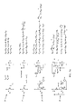
- Figure 3a shows step-by-step how the resistance of the MOS transistor can be linearized by super-positioning a fraction of its drain signal voltage to its gate.
- the equations relate to an idealized square-law MOS characteristic.
- Figure 3a shows analyses for both NMOS and PMOS configurations.
- V GS which equals V GS0 +v DS /2
- the on-resistance of the MOS transistor becomes almost constant.
- the top images 30 show the basic transistor characteristics as in Figure 2 .
- the images 32 show the influence of adding a component to an initial gate-source voltage V GS0 which component is a half of the drain source voltage V DS .
- the images 34 show a how a circuit based on capacitive coupling can couple half the change in drain source voltage onto the gate.
- a capacitor C is provided between the gate and drain. This capacitor forms a capacitive coupling circuit with the parasitic capacitances between the gate and drain and between the gate and source.
- the gate is biased to a low frequency (e.g. dc) reference level by a gate bias voltage V GS0 which forms part of a high impedance bias circuit.
- a large bias resistor R BIAS couples the reference voltage level to the gate.
- the gate has high-ohmic bias, so there is a cut-off frequency of Rbias together with all capacitance on the gate node, which is set to a low frequency, This means the signal spectrum is sufficiently higher that for the signal spectrum the gate signal is only capacitively determined.
- the signal spectrum is usually DC-balanced (i.e. no DC) by line encoding and/or modulation techniques, meaning that there is no significant signal content below a certain corner frequency.
- the capacitive ratios determine the coupling fraction.
- the most significant capacitors in the coupling scheme are Cgs and Cdg of the transistor and the coupling capacitor C.
- Cdg actually helps substantially, especially when a substantial part of the resistance is made with an explicit series resistor in the drain.
- the intrinsic coupling is lower, and therefore some additional signal needs to be coupled to the gate. This is achieved with the extra coupling capacitor C.
- the drain signal can be fractionally coupled to the gate by the capacitor between drain and gate which forms a capacitive division with the capacitances seen at the gate node with respect to other nodes.
- the ac resistance becomes dependent only on the constants V GT0 (the reference over-threshold drive) and V DS0 (the reference/dc drain source voltage).
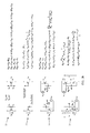
- the bottom images 36 show that the capacitor C which provides the desired coupling of 1/2v DS can replaced by a smaller capacitor ⁇ C, by introducing a resistor Rx between the drain and the capacitor terminal.
- the added series resistor can be of any type. Inaccuracies in the value of the resistance Rx can be compensated by the tuning of the emulated resistor, so that the total resistance is at the desired value.
- the optimum factor ⁇ is the ratio between Rds and Rx. Because Rx has spread, this ratio is not perfectly constant. By way of example, Rx can contribute about 60% and Rds contributes about 40% of the total resistance (of 50 Ohm). The misfit of ⁇ due to spread is acceptable in that case. Note that even with a series resistor the capacitive coupling can also be implemented from the point between the series resistor Rx and transistor. The capacitor needs to be somewhat larger, but the capacitive ratio becomes better determined in that case.
- Figure 4 merges the results obtained in Figure 3a and 3b to provide idealized expressions that hold for both positive and negative drain-source voltages.
- the structures shown will be referred to as the tuneable resistor topology or tuneable linearized resistor topology of the invention.
- the gate node of the MOS transistor is biased with a resistor R BIAS which is on the other side connected to the reference (dc) gate voltage V GS0.
- This bias resistor provides the correct DC level to the gate, but shall be sufficiently high-impedance in the frequency spectrum of this signal in order to ensure good partial signal coupling to this gate node.
- This bias resistor together with the total capacitance seen at the gate node, causes a high-pass characteristic in the partial signal coupling.
- R BIAS the value of R BIAS is therefore indicated to preferably go to 'infinity'.
- the latter is not really required, as it is not a limiting factor as long as the corner-frequency of this high-pass filter is kept sufficiently low.
- the gate-source voltage V GS is on the vertical axis
- the drain-source voltage V DS is on the horizontal axis
- the size of the grey areas is a measure of the current.
- MOS transistors Some practical non-idealities of MOS transistors actually help to improve performance.
- the limited output impedance in saturated operation means that there is not a hard cross-over point where the impedance suddenly becomes very large.
- Other effects like back-bias modulation can easily be accounted for by optimizing the component dimensions in a real circuit design.
- the resistor structure according to this invention has the extra advantage that the resistance does not remain constant for any voltage.
- V DS when the MOS transistor becomes saturated, it behaves by first approximation as a current source, thereby limiting the maximum current. This provides an implicit current limiting feature. This can be utilized as short circuit protection, for example, thereby also taking away the need to over-dimension the components and routing for currents far beyond the normal operating conditions.
- Figure 6 shows an example of signals at the drain and gate of the MOS transistor in the tuneable resistor topology for both sinusoidal and bit stream signals.
- the gate voltage (which is the gate-source voltage) comprises the reference level V GS0 modulated by the high frequency fluctuation v Ds /2
- the drain voltage (which is the drain-source voltage) comprises the reference level V DSO modulated by the high frequency fluctuation v DS .
- tuneable resistor topology of the invention can be applied in circuits and how appropriate biasing can be generated to achieve the desired resistance.
- One example of use of the circuit of the invention is in line driver circuits. for driving serial signals down transmission lines, to enable communication between different pieces of electronic equipment.
- a current sinking switched current driver a current source sinks current through the loads from the termination voltage.
- a current source sources current through the loads to the termination voltage.
- the tuneable resistor topology can be connected to any termination voltage
- the PMOS-based version for higher termination voltages (typically a current sinking arrangement) and the NMOS-based version for lower termination voltages (typically a current sourcing arrangement) with respect to the supply.
- the PMOS-based version this would typically be vdd and for the NMOS-based version that typically would be vss.
- the topology is shown as connected to a supply, in most cases that is the PMOS-based version with respect to vdd and in a few cases the NMOS-based version with respect to vss. This is for comprehensibility of the examples. However, this does not limit the scope of this invention, as these examples can also be reworked to terminate to any other termination voltage.
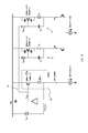
- Figure 7 shows a method to bias the gate voltage of the tuneable resistor topology to obtain a desired resistance for the case when there is common-mode DC current flowing through the resistors.
- the circuit is a current sinking switched line driver.
- the current source 70 sinks a drive current Idrive through one or other of the resistor circuits 72,74 in dependence on the signals applied to the gates of a pair of input transistors 76,78.
- the resistor circuits function as termination circuits.
- the output load (in this example including the shown near-end termination, but not shown are the transmission lines and far-end termination load) is connected between the output nodes dp and dn so that current is drawn through the load. For example with transistor 76 turned on, a current will be drawn through resistor circuit 74, along the transmission line between dn and dp and through transistor 76
- the far-end termination resistance typically equals to the near-end termination resistance, so the AC current will roughly split 50/50.
- the transmission path includes AC coupling, (DC blocking), so that all DC current flows through the near-end termination. Without AC coupling the DC current distribution depends also on the far-end termination voltage.
- a common mode voltage source 80 generates a common mode voltage which.
- Circuit 82 functions as a replica structure of the tuneable resistor terminations, and a current is drawn from the circuit 82 by a reference current source.
- This reference current is mirrored in the two resistor circuits 72,74, with scaling so that the current source 70 draws a current N times the reference current. This is achieved with suitable scaling of the transistor dimensions.
- the termination resistor circuits require accurate absolute value of resistance for impedance matching purposes.
- a scaled version of the common-mode currents through the resistor circuits 72,74 is enforced through a replica of the tuned-resistor topology, which is similarly scaled in size too, such that the impedance of the replica structure (i.e. between Vdd and the bottom of resistor NRx/2) is a scaled version of the resistor circuit impedance.
- This scaling factor is N in figure 7 .
- a feedback loop including an amplifier 84 which generates the gate bias V GCM for the replica structure 82, enforces that the voltage across the replica structure is equal to the provided reference voltage Vcm.
- Vcm/Iref has the nature of a resistance and can for example be derived from another, not-bandwidth limited , integrated digitally calibrated resistor Rref, which can be implemented according to Figure 1 .
- the current Iref can be generated by enforcing a bandgap voltage across the Rref, and the voltage Vcm can be generated as a scaled copy of a bandgap voltage.
- this biasing structure allows to accurately control the output voltage level, due to the replica biasing, which enforces Vcm across the replica, which corresponds with a common-mode level of approximately Vcm across the terminations.
- This method of control enables much better voltage accuracy than the summed inaccuracies of an independently generated current Iref and some reference impedance Rref.
- This provides the advantage that the signal voltage window is better constrained which allows for better optimized designs. Theoretically this has the impact that the resulting impedance will become slightly less accurate.
- the tuneable resistor topology of the invention provides sufficient accuracy, because Iref and Vcm can be correlated, so that this aspect will not be a limiting factor in practice.
- Figure 8 corresponds to Figure 7 , and the only difference is that instead of scaling the reference current for the replica, the impedance of the replica is scaled. This is achieved by scaling the transistor width (1/n) and the value of the series resistor (n). This represents schematically the ability to scale the impedance of replica circuit 82.
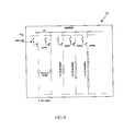
- Figure 9 shows a possible embodiment of the replica circuit 82 to allow replica-size scaling as shown schematically in Figure 8 .
- part of the tuning is done in a linear fashion, by N parallel unity segments, and part of the tuning is done in a binary manner, by binary-scaled segments.
- the circuit comprises a series of parallel branches, each with a transistor and resistor.
- the first N branches have the same dimension transistor (W/L) and the same resistor value NRx.
- the remaining branches have a binary decreasing W/L ratio (W/2L, W/4L etc.) and a binary increasing resistor value (2NRx, 4NRx etc.).
- Each transistor is controlled independently so that the different branches can be switched in or out of circuit.
- a control word "replica_size" provides control of all of the branches.
- the number N allows easy scaling for several drive strengths if the termination is also implemented as N equivalent parallel segments.
- the binary fractional part in the replica circuit 82 allows for fine-tuning and to cover all drive strengths with sufficient accuracy.
- Figure 10 corresponds to Figure 7 , but with the current source 70 and control switches 76,78 omitted.
- the replica circuit is shown as having a transistor with a width to length ratio of kW/L compared to the resistor circuit transistors with width to length ratio of NW/L.
- Figures 7 and 8 show a driver side configuration, where the devices 70, 76, 78 represent the current-switched driver.
- Figure 10 shows a receiver side configuration, so the driver related components are not shown. The receiver side may often have no DC current through the termination.
- the impedance as seen at dp and dn decreases for decreasing size of the replica, and the impedance increases for increasing size of the replica. Note that by increasing the "size" of the replica is meant increasing the size of the impedance of the replica.
- Vcm intentionally does not correspond with the actual common-mode voltage of nodes dp and dn.
- the replica can be made such that its effective size is controllable, for example as shown in Figure 9 with digital logic control signals.
- an adaptable value of Vcm can for example be implemented with a resistive ladder with a fixed reference voltage across, and the common mode voltage Vcm is taken from a selected ladder tap.
- the currents through the R BIAS resistors cancel each other and do not impact the feedback control loop.
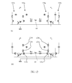
- Figure 11 shows a complementary structure using NMOS transistors, including two terminations using the tuneable resistor topology and a replica bias structure.
- the circuit functions according to the same principles as the circuits of Figure 7 , 8 , and 10 , and is simply provided to show an NMOS implementation, suitable for a current sinking switched current source line driver or a receiver-side termination to vss.
- the achievable impedance tuning range of the tuneable resistor topology as shown in Figure 4 is influenced by the choice of Rx and furthermore constrained by the triode voltage region limits of the MOS transistor. Note that the linearized signal voltage range is extended by increasing Rx as fraction of the total resistance, while simultaneously the achievable impedance tuning range reduces, and vice versa. Balancing these two aspects will preferably allows:
- the structure can be extended with selectable extra branches as shown in Figure 12 .
- Figure 12a shows a circuit where multiple similar, possibly scaled, branches are put in parallel within each emulated resistor circuit.
- the first branch 120a covers the highest impedance range, the second 120b one a lowered range as the total resistance of the parallel branches is decreased. As long as both ranges are overlapping the total tuneable range is extended. Note that the extension can be continued with a third branch, and so on.
- a select control line determines if the emulated resistor circuits comprise a single branch 120a and thus correspond to the examples above, or if the two branches (in this example) are connected together in parallel. Alternately, (not shown) the two branches may be implemented as independently selectable such that either one branch, the second branch, or both in parallel can be selected. This approach can also be extended to more than 2 branches.
- Figure 12b shows an alternate method to increase the tuning range by splitting the extra series resistor Rx into multiple fractions, and multiple transistors connected with their drain to these resistor taps.
- One transistor 122a connects to both resistors 124a,124b in series, and the circuit then functions in the same way as the earlier circuits (with the sum of the two resistors 124,124b equal to Rx).
- a second branch is activated which includes only resistor 124b. This effectively bypasses resistor 124a and thereby disables the first path.
- All enabled transistors are coupled to the gate control node V GCM , while for disabled transistors their V GS is made low by the select line. By selecting which transistor(s) are enabled the fraction of Rx in the total resistance can be varied.
- the structure can be made high impedance by making the V GS of the MOS transistor low, that way utilizing the same MOS transistor as a switch that can be turned-off.
- the tuneable resistor topology utilizes a MOS transistor as tuning device.
- the benefits of the partial signal coupling to the gate are caused by the non-linear device characteristics of the MOS transistor between control voltage Vgs, drain-source voltage Vds, drain current Id, and their correlation.
- any other type of transistor device can be used instead as long as it has a control gate to influence the (linear or non-linear) output I-V characteristics.
- the coupling factor, and/or coupling filter, and/or coupling function can then be optimized to eliminate or reduce the overall nonlinearity of the tuneable resistance structure.
- the main area of interest for application of the invention is for line termination in high-speed interfaces.
- the invention is not limited to application for termination resistors, but can also be used for any application where tuneability of resistance is required.
- the topology can also be advantageous to just linearize the output characteristics of a non- linear device, such as a MOS transistor.
- the transistor source is connected to a termination voltage which acts as reference level (e.g. a supply).
- a termination voltage which acts as reference level (e.g. a supply).
- a scaled fraction of the ac drain voltage is super-positioned on to the gate-source voltage to improve linearity, as in that case the ac drain voltage is equivalent to ac drain-source voltage.
- Other circuit connections are possible in which the source is no longer at a fixed voltage, and indeed the source voltage relative to a fixed voltage can then become the feedback voltage to be coupled to the gate.
- the invention is mainly of interest when using a transistor to emulate a resistor, but the invention can be applied to other devices which function as a controlled resistor, and which have a control terminal which influences the resistance between two other terminals.
Landscapes
- Engineering & Computer Science (AREA)
- Power Engineering (AREA)
- Computer Networks & Wireless Communication (AREA)
- Signal Processing (AREA)
- Amplifiers (AREA)
- Networks Using Active Elements (AREA)
- Logic Circuits (AREA)
Priority Applications (2)
| Application Number | Priority Date | Filing Date | Title |
|---|---|---|---|
| EP11188022.5A EP2456152B1 (de) | 2010-11-17 | 2011-11-07 | Integrierte Schaltung zur Emulierung eines Widerstands |
| US13/297,478 US20120119821A1 (en) | 2010-11-17 | 2011-11-16 | Integrated circuit for emulating a resistor |
Applications Claiming Priority (2)
| Application Number | Priority Date | Filing Date | Title |
|---|---|---|---|
| EP10191578 | 2010-11-17 | ||
| EP11188022.5A EP2456152B1 (de) | 2010-11-17 | 2011-11-07 | Integrierte Schaltung zur Emulierung eines Widerstands |
Publications (3)
| Publication Number | Publication Date |
|---|---|
| EP2456152A2 true EP2456152A2 (de) | 2012-05-23 |
| EP2456152A3 EP2456152A3 (de) | 2015-04-15 |
| EP2456152B1 EP2456152B1 (de) | 2017-01-11 |
Family
ID=44905713
Family Applications (1)
| Application Number | Title | Priority Date | Filing Date |
|---|---|---|---|
| EP11188022.5A Not-in-force EP2456152B1 (de) | 2010-11-17 | 2011-11-07 | Integrierte Schaltung zur Emulierung eines Widerstands |
Country Status (3)
| Country | Link |
|---|---|
| US (1) | US20120119821A1 (de) |
| EP (1) | EP2456152B1 (de) |
| CN (1) | CN102468820B (de) |
Cited By (3)
| Publication number | Priority date | Publication date | Assignee | Title |
|---|---|---|---|---|
| WO2016075056A1 (en) * | 2014-11-11 | 2016-05-19 | Maschinenfabrik Reinhausen Gmbh | Resistor emulation and gate boost |
| US10249769B1 (en) | 2017-12-13 | 2019-04-02 | Dialog Semiconductor, Inc. | On-chip tuneable diffusion resistor |
| US10410697B2 (en) | 2017-04-27 | 2019-09-10 | Ememory Technology Inc. | Sensing circuit with voltage clamp for non-volatile memory |
Families Citing this family (4)
| Publication number | Priority date | Publication date | Assignee | Title |
|---|---|---|---|---|
| WO2014163881A1 (en) * | 2013-03-11 | 2014-10-09 | The Regents Of The University Of California | Low jitter tunable voltage control oscillator with self calibration circuits to reduce chip fabrication process variation |
| CN104880963A (zh) * | 2014-10-27 | 2015-09-02 | 上海葩星信息科技有限公司 | 一种电阻仿真器 |
| US10003312B2 (en) | 2015-08-31 | 2018-06-19 | Qualcomm Incorporated | Amplifier with feedback circuit |
| CN112558342B (zh) * | 2020-12-23 | 2023-11-28 | 深圳市华星光电半导体显示技术有限公司 | 像素电路的仿真系统及仿真方法 |
Family Cites Families (10)
| Publication number | Priority date | Publication date | Assignee | Title |
|---|---|---|---|---|
| US4574249A (en) * | 1981-09-08 | 1986-03-04 | At&T Bell Laboratories | Nonintegrating lightwave receiver |
| US5065055A (en) * | 1990-12-20 | 1991-11-12 | Sun Microsystems, Inc. | Method and apparatus for high-speed bi-CMOS differential amplifier with controlled output voltage swing |
| US6897697B2 (en) * | 1999-06-28 | 2005-05-24 | Broadcom Corporation | Current-controlled CMOS circuit using higher voltage supply in low voltage CMOS process |
| US6340899B1 (en) * | 2000-02-24 | 2002-01-22 | Broadcom Corporation | Current-controlled CMOS circuits with inductive broadbanding |
| US6414512B1 (en) * | 2000-04-04 | 2002-07-02 | Pixelworks, Inc. | On-chip termination circuit |
| US6346832B1 (en) * | 2000-05-22 | 2002-02-12 | Motorola, Inc. | Multi-channel signaling |
| US6683472B2 (en) * | 2002-02-19 | 2004-01-27 | Rambus Inc. | Method and apparatus for selectably providing single-ended and differential signaling with controllable impedance and transition time |
| US8225248B2 (en) * | 2005-10-24 | 2012-07-17 | Cadence Design Systems, Inc. | Timing, noise, and power analysis of integrated circuits |
| US7675372B2 (en) * | 2006-08-09 | 2010-03-09 | Qualcomm Incorporated | Circuit simulator parameter extraction using a configurable ring oscillator |
| US7750738B2 (en) * | 2008-11-20 | 2010-07-06 | Infineon Technologies Ag | Process, voltage and temperature control for high-speed, low-power fixed and variable gain amplifiers based on MOSFET resistors |
-
2011
- 2011-11-07 EP EP11188022.5A patent/EP2456152B1/de not_active Not-in-force
- 2011-11-16 CN CN201110363002.3A patent/CN102468820B/zh not_active Expired - Fee Related
- 2011-11-16 US US13/297,478 patent/US20120119821A1/en not_active Abandoned
Non-Patent Citations (1)
| Title |
|---|
| None |
Cited By (3)
| Publication number | Priority date | Publication date | Assignee | Title |
|---|---|---|---|---|
| WO2016075056A1 (en) * | 2014-11-11 | 2016-05-19 | Maschinenfabrik Reinhausen Gmbh | Resistor emulation and gate boost |
| US10410697B2 (en) | 2017-04-27 | 2019-09-10 | Ememory Technology Inc. | Sensing circuit with voltage clamp for non-volatile memory |
| US10249769B1 (en) | 2017-12-13 | 2019-04-02 | Dialog Semiconductor, Inc. | On-chip tuneable diffusion resistor |
Also Published As
| Publication number | Publication date |
|---|---|
| CN102468820A (zh) | 2012-05-23 |
| US20120119821A1 (en) | 2012-05-17 |
| EP2456152A3 (de) | 2015-04-15 |
| CN102468820B (zh) | 2015-08-05 |
| EP2456152B1 (de) | 2017-01-11 |
Similar Documents
| Publication | Publication Date | Title |
|---|---|---|
| EP2456152B1 (de) | Integrierte Schaltung zur Emulierung eines Widerstands | |
| US7969195B1 (en) | Active biasing in metal oxide semiconductor (MOS) differential pairs | |
| US9966908B1 (en) | Circuit for and method of implementing a differential input receiver | |
| US7911244B2 (en) | Differential drive circuit and communication device | |
| CN101471667B (zh) | D/a转换电路 | |
| JP5233531B2 (ja) | 差動駆動回路および通信装置 | |
| US7030660B2 (en) | Line driver | |
| US8179205B2 (en) | Linearization systems and methods for variable attenuators | |
| US20150280666A1 (en) | Differential amplification circuit and semiconductor integrated circuit | |
| US10778207B1 (en) | Passive dynamic biasing for MOSFET cascode | |
| US20090033367A1 (en) | Transmission Device | |
| US6307402B1 (en) | Output buffer for driving a symmetrical transmission line | |
| US8427204B2 (en) | Mixed-mode input buffer | |
| KR20170134420A (ko) | 프로그램가능 고속 등화기 및 관련된 방법 | |
| CN102759943B (zh) | 具有反馈的电流引导电路 | |
| CN101651452B (zh) | 一种rc积分电路 | |
| US20060192705A1 (en) | Current source cell and D/A converter using the same | |
| US20110163807A1 (en) | Impedance matching circuit and method thereof | |
| US8624628B1 (en) | Adjustable level shifter | |
| US9847758B2 (en) | Low noise amplifier | |
| JP6072387B1 (ja) | 可変利得増幅器 | |
| US8665015B1 (en) | Power amplifier circuit | |
| JP5126355B2 (ja) | 終端回路、半導体装置、及び電子機器 | |
| US7224220B2 (en) | Low distortion variable gain and rooting amplifier with solid state relay | |
| US8283980B2 (en) | Amplifier circuit |
Legal Events
| Date | Code | Title | Description |
|---|---|---|---|
| PUAI | Public reference made under article 153(3) epc to a published international application that has entered the european phase |
Free format text: ORIGINAL CODE: 0009012 |
|
| AK | Designated contracting states |
Kind code of ref document: A2 Designated state(s): AL AT BE BG CH CY CZ DE DK EE ES FI FR GB GR HR HU IE IS IT LI LT LU LV MC MK MT NL NO PL PT RO RS SE SI SK SM TR |
|
| AX | Request for extension of the european patent |
Extension state: BA ME |
|
| 17P | Request for examination filed |
Effective date: 20140331 |
|
| PUAL | Search report despatched |
Free format text: ORIGINAL CODE: 0009013 |
|
| AK | Designated contracting states |
Kind code of ref document: A3 Designated state(s): AL AT BE BG CH CY CZ DE DK EE ES FI FR GB GR HR HU IE IS IT LI LT LU LV MC MK MT NL NO PL PT RO RS SE SI SK SM TR |
|
| AX | Request for extension of the european patent |
Extension state: BA ME |
|
| RIC1 | Information provided on ipc code assigned before grant |
Ipc: H04L 25/02 20060101AFI20150310BHEP |
|
| RBV | Designated contracting states (corrected) |
Designated state(s): AL AT BE BG CH CY CZ DE DK EE ES FI FR GB GR HR HU IE IS IT LI LT LU LV MC MK MT NL NO PL PT RO RS SE SI SK SM TR |
|
| 17Q | First examination report despatched |
Effective date: 20160525 |
|
| GRAP | Despatch of communication of intention to grant a patent |
Free format text: ORIGINAL CODE: EPIDOSNIGR1 |
|
| INTG | Intention to grant announced |
Effective date: 20160912 |
|
| STAA | Information on the status of an ep patent application or granted ep patent |
Free format text: STATUS: GRANT OF PATENT IS INTENDED |
|
| GRAS | Grant fee paid |
Free format text: ORIGINAL CODE: EPIDOSNIGR3 |
|
| GRAA | (expected) grant |
Free format text: ORIGINAL CODE: 0009210 |
|
| STAA | Information on the status of an ep patent application or granted ep patent |
Free format text: STATUS: THE PATENT HAS BEEN GRANTED |
|
| AK | Designated contracting states |
Kind code of ref document: B1 Designated state(s): AL AT BE BG CH CY CZ DE DK EE ES FI FR GB GR HR HU IE IS IT LI LT LU LV MC MK MT NL NO PL PT RO RS SE SI SK SM TR |
|
| REG | Reference to a national code |
Ref country code: GB Ref legal event code: FG4D |
|
| REG | Reference to a national code |
Ref country code: CH Ref legal event code: EP |
|
| REG | Reference to a national code |
Ref country code: AT Ref legal event code: REF Ref document number: 862178 Country of ref document: AT Kind code of ref document: T Effective date: 20170115 |
|
| REG | Reference to a national code |
Ref country code: IE Ref legal event code: FG4D |
|
| REG | Reference to a national code |
Ref country code: DE Ref legal event code: R096 Ref document number: 602011034235 Country of ref document: DE |
|
| REG | Reference to a national code |
Ref country code: LT Ref legal event code: MG4D |
|
| REG | Reference to a national code |
Ref country code: NL Ref legal event code: MP Effective date: 20170111 |
|
| REG | Reference to a national code |
Ref country code: AT Ref legal event code: MK05 Ref document number: 862178 Country of ref document: AT Kind code of ref document: T Effective date: 20170111 |
|
| PG25 | Lapsed in a contracting state [announced via postgrant information from national office to epo] |
Ref country code: NL Free format text: LAPSE BECAUSE OF FAILURE TO SUBMIT A TRANSLATION OF THE DESCRIPTION OR TO PAY THE FEE WITHIN THE PRESCRIBED TIME-LIMIT Effective date: 20170111 |
|
| PG25 | Lapsed in a contracting state [announced via postgrant information from national office to epo] |
Ref country code: LT Free format text: LAPSE BECAUSE OF FAILURE TO SUBMIT A TRANSLATION OF THE DESCRIPTION OR TO PAY THE FEE WITHIN THE PRESCRIBED TIME-LIMIT Effective date: 20170111 Ref country code: NO Free format text: LAPSE BECAUSE OF FAILURE TO SUBMIT A TRANSLATION OF THE DESCRIPTION OR TO PAY THE FEE WITHIN THE PRESCRIBED TIME-LIMIT Effective date: 20170411 Ref country code: FI Free format text: LAPSE BECAUSE OF FAILURE TO SUBMIT A TRANSLATION OF THE DESCRIPTION OR TO PAY THE FEE WITHIN THE PRESCRIBED TIME-LIMIT Effective date: 20170111 Ref country code: GR Free format text: LAPSE BECAUSE OF FAILURE TO SUBMIT A TRANSLATION OF THE DESCRIPTION OR TO PAY THE FEE WITHIN THE PRESCRIBED TIME-LIMIT Effective date: 20170412 Ref country code: HR Free format text: LAPSE BECAUSE OF FAILURE TO SUBMIT A TRANSLATION OF THE DESCRIPTION OR TO PAY THE FEE WITHIN THE PRESCRIBED TIME-LIMIT Effective date: 20170111 Ref country code: IS Free format text: LAPSE BECAUSE OF FAILURE TO SUBMIT A TRANSLATION OF THE DESCRIPTION OR TO PAY THE FEE WITHIN THE PRESCRIBED TIME-LIMIT Effective date: 20170511 |
|
| PG25 | Lapsed in a contracting state [announced via postgrant information from national office to epo] |
Ref country code: LV Free format text: LAPSE BECAUSE OF FAILURE TO SUBMIT A TRANSLATION OF THE DESCRIPTION OR TO PAY THE FEE WITHIN THE PRESCRIBED TIME-LIMIT Effective date: 20170111 Ref country code: SE Free format text: LAPSE BECAUSE OF FAILURE TO SUBMIT A TRANSLATION OF THE DESCRIPTION OR TO PAY THE FEE WITHIN THE PRESCRIBED TIME-LIMIT Effective date: 20170111 Ref country code: PL Free format text: LAPSE BECAUSE OF FAILURE TO SUBMIT A TRANSLATION OF THE DESCRIPTION OR TO PAY THE FEE WITHIN THE PRESCRIBED TIME-LIMIT Effective date: 20170111 Ref country code: BG Free format text: LAPSE BECAUSE OF FAILURE TO SUBMIT A TRANSLATION OF THE DESCRIPTION OR TO PAY THE FEE WITHIN THE PRESCRIBED TIME-LIMIT Effective date: 20170411 Ref country code: PT Free format text: LAPSE BECAUSE OF FAILURE TO SUBMIT A TRANSLATION OF THE DESCRIPTION OR TO PAY THE FEE WITHIN THE PRESCRIBED TIME-LIMIT Effective date: 20170511 Ref country code: ES Free format text: LAPSE BECAUSE OF FAILURE TO SUBMIT A TRANSLATION OF THE DESCRIPTION OR TO PAY THE FEE WITHIN THE PRESCRIBED TIME-LIMIT Effective date: 20170111 Ref country code: AT Free format text: LAPSE BECAUSE OF FAILURE TO SUBMIT A TRANSLATION OF THE DESCRIPTION OR TO PAY THE FEE WITHIN THE PRESCRIBED TIME-LIMIT Effective date: 20170111 Ref country code: RS Free format text: LAPSE BECAUSE OF FAILURE TO SUBMIT A TRANSLATION OF THE DESCRIPTION OR TO PAY THE FEE WITHIN THE PRESCRIBED TIME-LIMIT Effective date: 20170111 |
|
| REG | Reference to a national code |
Ref country code: DE Ref legal event code: R097 Ref document number: 602011034235 Country of ref document: DE |
|
| REG | Reference to a national code |
Ref country code: FR Ref legal event code: PLFP Year of fee payment: 7 |
|
| PG25 | Lapsed in a contracting state [announced via postgrant information from national office to epo] |
Ref country code: RO Free format text: LAPSE BECAUSE OF FAILURE TO SUBMIT A TRANSLATION OF THE DESCRIPTION OR TO PAY THE FEE WITHIN THE PRESCRIBED TIME-LIMIT Effective date: 20170111 Ref country code: IT Free format text: LAPSE BECAUSE OF FAILURE TO SUBMIT A TRANSLATION OF THE DESCRIPTION OR TO PAY THE FEE WITHIN THE PRESCRIBED TIME-LIMIT Effective date: 20170111 Ref country code: CZ Free format text: LAPSE BECAUSE OF FAILURE TO SUBMIT A TRANSLATION OF THE DESCRIPTION OR TO PAY THE FEE WITHIN THE PRESCRIBED TIME-LIMIT Effective date: 20170111 Ref country code: EE Free format text: LAPSE BECAUSE OF FAILURE TO SUBMIT A TRANSLATION OF THE DESCRIPTION OR TO PAY THE FEE WITHIN THE PRESCRIBED TIME-LIMIT Effective date: 20170111 Ref country code: SK Free format text: LAPSE BECAUSE OF FAILURE TO SUBMIT A TRANSLATION OF THE DESCRIPTION OR TO PAY THE FEE WITHIN THE PRESCRIBED TIME-LIMIT Effective date: 20170111 |
|
| PLBE | No opposition filed within time limit |
Free format text: ORIGINAL CODE: 0009261 |
|
| STAA | Information on the status of an ep patent application or granted ep patent |
Free format text: STATUS: NO OPPOSITION FILED WITHIN TIME LIMIT |
|
| PG25 | Lapsed in a contracting state [announced via postgrant information from national office to epo] |
Ref country code: DK Free format text: LAPSE BECAUSE OF FAILURE TO SUBMIT A TRANSLATION OF THE DESCRIPTION OR TO PAY THE FEE WITHIN THE PRESCRIBED TIME-LIMIT Effective date: 20170111 Ref country code: SM Free format text: LAPSE BECAUSE OF FAILURE TO SUBMIT A TRANSLATION OF THE DESCRIPTION OR TO PAY THE FEE WITHIN THE PRESCRIBED TIME-LIMIT Effective date: 20170111 |
|
| 26N | No opposition filed |
Effective date: 20171012 |
|
| PG25 | Lapsed in a contracting state [announced via postgrant information from national office to epo] |
Ref country code: SI Free format text: LAPSE BECAUSE OF FAILURE TO SUBMIT A TRANSLATION OF THE DESCRIPTION OR TO PAY THE FEE WITHIN THE PRESCRIBED TIME-LIMIT Effective date: 20170111 |
|
| PG25 | Lapsed in a contracting state [announced via postgrant information from national office to epo] |
Ref country code: MC Free format text: LAPSE BECAUSE OF FAILURE TO SUBMIT A TRANSLATION OF THE DESCRIPTION OR TO PAY THE FEE WITHIN THE PRESCRIBED TIME-LIMIT Effective date: 20170111 |
|
| GBPC | Gb: european patent ceased through non-payment of renewal fee |
Effective date: 20171107 |
|
| PG25 | Lapsed in a contracting state [announced via postgrant information from national office to epo] |
Ref country code: LI Free format text: LAPSE BECAUSE OF NON-PAYMENT OF DUE FEES Effective date: 20171130 Ref country code: CH Free format text: LAPSE BECAUSE OF NON-PAYMENT OF DUE FEES Effective date: 20171130 |
|
| PG25 | Lapsed in a contracting state [announced via postgrant information from national office to epo] |
Ref country code: LU Free format text: LAPSE BECAUSE OF NON-PAYMENT OF DUE FEES Effective date: 20171107 |
|
| REG | Reference to a national code |
Ref country code: BE Ref legal event code: MM Effective date: 20171130 |
|
| REG | Reference to a national code |
Ref country code: IE Ref legal event code: MM4A |
|
| PG25 | Lapsed in a contracting state [announced via postgrant information from national office to epo] |
Ref country code: MT Free format text: LAPSE BECAUSE OF NON-PAYMENT OF DUE FEES Effective date: 20171107 |
|
| REG | Reference to a national code |
Ref country code: FR Ref legal event code: PLFP Year of fee payment: 8 |
|
| PG25 | Lapsed in a contracting state [announced via postgrant information from national office to epo] |
Ref country code: IE Free format text: LAPSE BECAUSE OF NON-PAYMENT OF DUE FEES Effective date: 20171107 |
|
| PG25 | Lapsed in a contracting state [announced via postgrant information from national office to epo] |
Ref country code: GB Free format text: LAPSE BECAUSE OF NON-PAYMENT OF DUE FEES Effective date: 20171107 Ref country code: BE Free format text: LAPSE BECAUSE OF NON-PAYMENT OF DUE FEES Effective date: 20171130 |
|
| PGFP | Annual fee paid to national office [announced via postgrant information from national office to epo] |
Ref country code: DE Payment date: 20181023 Year of fee payment: 8 |
|
| PGFP | Annual fee paid to national office [announced via postgrant information from national office to epo] |
Ref country code: FR Payment date: 20181024 Year of fee payment: 8 |
|
| PG25 | Lapsed in a contracting state [announced via postgrant information from national office to epo] |
Ref country code: HU Free format text: LAPSE BECAUSE OF FAILURE TO SUBMIT A TRANSLATION OF THE DESCRIPTION OR TO PAY THE FEE WITHIN THE PRESCRIBED TIME-LIMIT; INVALID AB INITIO Effective date: 20111107 |
|
| PG25 | Lapsed in a contracting state [announced via postgrant information from national office to epo] |
Ref country code: CY Free format text: LAPSE BECAUSE OF NON-PAYMENT OF DUE FEES Effective date: 20170111 |
|
| PG25 | Lapsed in a contracting state [announced via postgrant information from national office to epo] |
Ref country code: MK Free format text: LAPSE BECAUSE OF FAILURE TO SUBMIT A TRANSLATION OF THE DESCRIPTION OR TO PAY THE FEE WITHIN THE PRESCRIBED TIME-LIMIT Effective date: 20170111 |
|
| PG25 | Lapsed in a contracting state [announced via postgrant information from national office to epo] |
Ref country code: TR Free format text: LAPSE BECAUSE OF FAILURE TO SUBMIT A TRANSLATION OF THE DESCRIPTION OR TO PAY THE FEE WITHIN THE PRESCRIBED TIME-LIMIT Effective date: 20170111 |
|
| REG | Reference to a national code |
Ref country code: DE Ref legal event code: R119 Ref document number: 602011034235 Country of ref document: DE |
|
| PG25 | Lapsed in a contracting state [announced via postgrant information from national office to epo] |
Ref country code: AL Free format text: LAPSE BECAUSE OF FAILURE TO SUBMIT A TRANSLATION OF THE DESCRIPTION OR TO PAY THE FEE WITHIN THE PRESCRIBED TIME-LIMIT Effective date: 20170111 |
|
| PG25 | Lapsed in a contracting state [announced via postgrant information from national office to epo] |
Ref country code: FR Free format text: LAPSE BECAUSE OF NON-PAYMENT OF DUE FEES Effective date: 20191130 Ref country code: DE Free format text: LAPSE BECAUSE OF NON-PAYMENT OF DUE FEES Effective date: 20200603 |