EP2452268B1 - Detection of usb attachment - Google Patents
Detection of usb attachment Download PDFInfo
- Publication number
- EP2452268B1 EP2452268B1 EP10732355.2A EP10732355A EP2452268B1 EP 2452268 B1 EP2452268 B1 EP 2452268B1 EP 10732355 A EP10732355 A EP 10732355A EP 2452268 B1 EP2452268 B1 EP 2452268B1
- Authority
- EP
- European Patent Office
- Prior art keywords
- interface
- change
- frequency clock
- attachment state
- high frequency
- Prior art date
- Legal status (The legal status is an assumption and is not a legal conclusion. Google has not performed a legal analysis and makes no representation as to the accuracy of the status listed.)
- Active
Links
Images


Classifications
-
- G—PHYSICS
- G06—COMPUTING OR CALCULATING; COUNTING
- G06F—ELECTRIC DIGITAL DATA PROCESSING
- G06F13/00—Interconnection of, or transfer of information or other signals between, memories, input/output devices or central processing units
- G06F13/38—Information transfer, e.g. on bus
- G06F13/382—Information transfer, e.g. on bus using universal interface adapter
- G06F13/385—Information transfer, e.g. on bus using universal interface adapter for adaptation of a particular data processing system to different peripheral devices
-
- Y—GENERAL TAGGING OF NEW TECHNOLOGICAL DEVELOPMENTS; GENERAL TAGGING OF CROSS-SECTIONAL TECHNOLOGIES SPANNING OVER SEVERAL SECTIONS OF THE IPC; TECHNICAL SUBJECTS COVERED BY FORMER USPC CROSS-REFERENCE ART COLLECTIONS [XRACs] AND DIGESTS
- Y02—TECHNOLOGIES OR APPLICATIONS FOR MITIGATION OR ADAPTATION AGAINST CLIMATE CHANGE
- Y02D—CLIMATE CHANGE MITIGATION TECHNOLOGIES IN INFORMATION AND COMMUNICATION TECHNOLOGIES [ICT], I.E. INFORMATION AND COMMUNICATION TECHNOLOGIES AIMING AT THE REDUCTION OF THEIR OWN ENERGY USE
- Y02D10/00—Energy efficient computing, e.g. low power processors, power management or thermal management
Definitions
- the present invention relates to USB (Universal Serial Bus) attachment detection. More particularly, it concerns a device having an USB port for data communication with another device, and more particularly the management of the electrical consumption of such a device.
- USB Universal Serial Bus
- USB designates a data communication protocol in serial form, defined by the specifications of the USB standard (version 2.0 of the USB Specification).
- FIG. 1 illustrates a system 11 of the classic USB type in which a first USB device 10 and a second USB device 14 are connected by an USB interface 15.
- This interface is generally composed of a cable with four wires equipped at each end with a plug able to cooperate with an USB connector with four or five contacts arranged on the first USB device 10 and on the second USB device 14.
- the USB interface 15 therefore comprises four or five physical lines: a ground GND, a power supply line VBus, two data lines D+ and D-, and an optional identification line ID.
- the first USB device 10 can correspond to a mobile phone when the second device 14 can be a headset or a computer.
- the first USB device 10 comprises a control unit 12 which is an unit that is generally primarily software, and an interface unit 13 which is for the most part generally implemented in the form of hardware. This control unit and this interface unit are connected to each other via an interface 16. This first device is powered via a plug 'PWR'. It also has a high frequency clock 105 and a low frequency clock 104 which are provided for a multiplexer 102.
- the first USB device 10 controls certain timings by means of a high frequency clock which is used for the exchanges between the first device 10 and the second device 14.
- This high frequency clock can be on the order of 38 MHz.
- the USB standard is supplemented by an OTG supplemental specification, described in the document " On-The-Go and Embedded Host Supplement to the USB Revision 2.0 Specification - Revision 2.0 - May 8, 2009 " which additionally contains in its paragraph 5.4 a definition of a protocol whose acronym is ADP for "Attach Detection Protocol", allowing the detection of the attachment of the second USB device 14 to the first USB device 10, and reciprocally.
- ADP protocol allows for the detection of this event by observing changes in capacitance in the power supply line VBus of the interface 15. More specifically, this event is detected by periodically looking for, after having discharged the VBus line, any variation in the time necessary for the VBus line to return to a predetermined voltage level.
- ADP probing This periodic attachment detection is known as "ADP probing" in the vocabulary of the USB standard.
- the operations conducted by the first USB device 10 consisting of detecting the ADP probing attempts by the second USB device 14 are called “ADP sensing”. They also allow the first USB device 10 to know whether the second USB device 14 is attached or not.
- the OTG supplemental specification specifies that the ADP probing must be executed at a frequency of every 1.9 to 2.6 seconds, typically every 2 seconds.
- the ADP probing as well as the ADP sensing are done at periodic requests of the control unit 12 using the high frequency clock. It therefore results that the first device 10 cannot enter into a state where the high frequency clock is deactivated as long as it is performing these operations.
- a first aspect of the invention proposes a method for managing a change of the attachment state between a first device and a second device connected to each other via an interface.
- the first device comprises a high frequency clock.
- the first device is in a sleep state in which the high frequency clock is deactivated.
- the method comprises the following steps at the first device:
- the first device When the first device is in a sleep state, it should be awakened if a change in the attachment state of the second device is detected, so that the first device can take the change into account and handle it properly.
- the first device to handle this event, although it is in a sleep state in which the high frequency clock is deactivated, it is advantageously provided that a low frequency clock allows periodically testing for this event, with the sleep state ending only if such an event has actually occurred.
- the first device can advantageously remain in the sleep state as long as the second device(s) do not change their attachment state. By proceeding in this manner, the amount of energy consumed can be considerably reduced.
- the first device is a mobile device, such as a portable computer or a mobile phone or a video camera or any other portable terminal which presents at least one USB port
- the implementation of such a management method according to an embodiment of the invention is highly advantageous with regards to the gain in autonomy that it can represent.
- the event relative to a change in the attachment state of the second device can be identified by detecting a capacitance change in the interface, in particular, by implementing the ADP protocol defined by a supplemental specification "On-The-Go and Embedded Host Supplement to the USB Revision 2.0 Specification - Revision 2.0 - May 8, 2009".
- the first device comprises a control functionality and an interface functionality with the second device, with said functionalities being connected to each other via an interface.
- the step /1/ is then realized by the interface functionality.
- the interface functionality notifies the control functionality of the change in attachment state of the second device, via an interrupt line.
- the interface is for example an ULPI interface comprising the interrupt line.
- a second aspect of the invention proposes an interface unit comprising means adapted to implement a method for managing changes in the USB attachment state according to the first aspect of the invention.
- Such an interface unit can correspond to an USB Transceiver within a first USB device.
- This interface unit can be connected to an USB control unit, or USB Controller, via an UTMI interface (USB2.0 Transceiver Macrocell Interface) or via an ULPI interface (UTMI Low Pin Interface).
- USB control unit or USB Controller
- UTMI interface USB 2.0 Transceiver Macrocell Interface
- ULPI interface UTMI Low Pin Interface
- the interface unit and the control unit can for example be implemented on the same chip and connected by an UTMI interface. They can also be implemented on two separate chips, and these chips can for example be connected via an ULPI interface.
- a third aspect of the invention proposes a device comprising means adapted to implement a method for managing changes in the USB attachment state according to the first aspect of the invention, in particular an interface unit according to the second aspect.
- a fourth aspect of the invention proposes a system comprising a first device according to the third aspect of the invention and at least one second device.
- the invention is defined according to the method of claim 1 and the interface unit of claim 6.
- a first device 10 and a second device 14 are considered.
- the first device can be a mobile phone and the second device 14 an USB voice headset or a computer.
- the architecture of the first device is based on two chips for the control unit and the interface unit respectively, connected to each other via an ULPI interface and possibly an interrupt line.
- Interrupt line is understood to mean an active electrical line whose change in level indicates a state change in the system. It is easy to apply it to any other possible device architecture, including an architecture using an UTMI interface for example.
- Figure 2-A illustrates the main steps of a method for managing a change in the attachment state of a second device to the first device, implemented according to an embodiment of the invention.
- the first device is in a sleep state in which the high frequency clock is deactivated.
- the detection is triggered of any change in the attachment state of the second device on the interface. This event corresponds for example to the plugging in of the second device to the first device using a cable, if the second device was not yet so connected, or conversely the removal of said cable if the second device was so connected until that moment.
- the method waits for a period during a step 22, with the aid of a low frequency clock. At the end of this period, the method can again be executed starting from the step 21.
- the first device is awakened from its sleep state in a step 23, in particular by activating the high frequency clock.
- a notification in the form of triggering a hardware interrupt, can be sent to the control unit from the first device during the step 23.
- the step 21 can be realized by performing ADP probing at the interface unit.
- a capacitance change is looked for in the VBus power supply line of the interface 15, in accordance with the supplemental specification "On-The-Go and Embedded Host Supplement to the USB Revision 2.0 Specification - Revision 2.0 - May 8, 2009."
- the step 21 can be realized by performing ADP sensing at the interface unit. Changes are looked for in the ADP probing activity performed by a possible second USB device on the interface 15, in accordance with the supplemental specification "On-The-Go and Embedded Host Supplement to the USB Revision 2.0 Specification - Revision 2.0 - May 8, 2009." Thus if ADP probing activity is no longer occurring when such was previously the case, this translates as a variation in the attachment state of the second device at the interface. Conversely, if ADP probing activity is occurring when such was not previously the case, this also translates as a variation in the attachment state of the second device at the interface.
- FIG. 2-B illustrates an USB system according to an embodiment of the invention.
- the same references as those used in Figure 1 relate to the same elements.
- the architecture of the first device is composed of two chips 12 and 13 connected to each other by an interface 16 on the basis of the high frequency clock which can be ULPI.
- the invention applies just as easily to any other architecture of the first device. No limitation is placed on this aspect.
- the low frequency clock is advantageously provided here via a link 201 to the interface unit 13.
- this low frequency clock can be used to count periods of time when the high frequency clock is off, thus meeting the requirements of the standard while saving energy.
- the interface 16 comprises an interrupt line on which the interface unit 13 can generate an interrupt in the form of an electrical signal to the control unit 12.
- this interrupt line can be the D3 ULPI interrupt line.
- a dedicated interrupt line 17 between the interface unit 13 and the control unit 12 can be used. No matter what the embodiment, after a change in the attachment state of the second device, the interrupt line is used to trigger an interrupt causing the USB system to wake from its sleep state, and more particularly the control unit 12 with an activation of the high frequency clock.
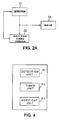
- Figure 3 illustrates a sequence diagram of an implementation of a method for detecting the attachment of a second device to the first device implemented according to an embodiment of the invention.
- the control unit 12 is in a sleep state in which the high frequency clock is deactivated, thus advantageously allowing the reduction of the energy consumption of this first device.
- the low frequency clock of the first device can remain continuously available, because the energy it uses is negligible compared to the energy consumed by the high frequency clock.
- the interface unit 13 waits for a period of time T, on the basis of the low frequency clock.
- the time T is between 1.9 and 2.6 seconds.
- the interface unit 13 triggers a detection of any change in the attachment state of the second device on the interface.
- This periodic attachment detection can, depending on the configuration of the first device 10, be ADP probing or alternatively ADP sensing.
- the interface unit 13 triggers a new detection at time t 2 after a wait period, then for the same reasons, at time t 3 after a wait period.
- a change in state is detected at the interface unit 13.
- the interface unit 13 then triggers the sending of an interrupt to the control unit 12.
- control unit 12 receives the interrupt, and activates the high frequency clock, causing it to awaken from its sleep state.
- the control unit 12 can then handle in the conventional manner the change in the attachment state of the second device.
- Figure 4 illustrates an interface unit 13 in a first device 10 additionally comprising a control unit and means for communicating with a second device via an interface 15 on the basis of a high frequency clock. It comprises:
- the high frequency clock of the interface unit 13 is activated upon detection by the detection unit of a change in the attachment state of the second device to the first device.
- a first device can comprise such an interface unit.
Landscapes
- Engineering & Computer Science (AREA)
- Theoretical Computer Science (AREA)
- Physics & Mathematics (AREA)
- General Engineering & Computer Science (AREA)
- General Physics & Mathematics (AREA)
- Power Sources (AREA)
- Information Transfer Systems (AREA)
Applications Claiming Priority (2)
| Application Number | Priority Date | Filing Date | Title |
|---|---|---|---|
| FR0954857A FR2947930B1 (fr) | 2009-07-10 | 2009-07-10 | Detection d'attachement usb |
| PCT/EP2010/059931 WO2011004020A2 (en) | 2009-07-10 | 2010-07-09 | Detection of usb attachment |
Publications (2)
| Publication Number | Publication Date |
|---|---|
| EP2452268A2 EP2452268A2 (en) | 2012-05-16 |
| EP2452268B1 true EP2452268B1 (en) | 2013-09-04 |
Family
ID=42115117
Family Applications (1)
| Application Number | Title | Priority Date | Filing Date |
|---|---|---|---|
| EP10732355.2A Active EP2452268B1 (en) | 2009-07-10 | 2010-07-09 | Detection of usb attachment |
Country Status (5)
| Country | Link |
|---|---|
| US (1) | US8762594B2 (enExample) |
| EP (1) | EP2452268B1 (enExample) |
| JP (1) | JP2012533106A (enExample) |
| FR (1) | FR2947930B1 (enExample) |
| WO (1) | WO2011004020A2 (enExample) |
Families Citing this family (13)
| Publication number | Priority date | Publication date | Assignee | Title |
|---|---|---|---|---|
| US8601186B2 (en) * | 2009-06-26 | 2013-12-03 | St-Ericsson Sa | Management of a USB host device |
| US9081911B2 (en) | 2011-05-31 | 2015-07-14 | Architecture Technology Corporation | Mediating communication of a universal serial bus device |
| US8862803B2 (en) * | 2011-05-31 | 2014-10-14 | Architecture Technology Corporation | Mediating communciation of a univeral serial bus device |
| US10108243B1 (en) * | 2012-08-31 | 2018-10-23 | Silego Technology, Inc. | Smart USB plug detection |
| US20140101345A1 (en) * | 2012-10-08 | 2014-04-10 | Analog Devices, Inc. | Universal serial bus (usb) plug-in event detection system and associated method |
| US11076113B2 (en) | 2013-09-26 | 2021-07-27 | Rosemount Inc. | Industrial process diagnostics using infrared thermal sensing |
| US10823592B2 (en) | 2013-09-26 | 2020-11-03 | Rosemount Inc. | Process device with process variable measurement using image capture device |
| US10638093B2 (en) | 2013-09-26 | 2020-04-28 | Rosemount Inc. | Wireless industrial process field device with imaging |
| US9488527B2 (en) | 2014-03-25 | 2016-11-08 | Rosemount Inc. | Process temperature measurement using infrared detector |
| US9857228B2 (en) | 2014-03-25 | 2018-01-02 | Rosemount Inc. | Process conduit anomaly detection using thermal imaging |
| US10914635B2 (en) * | 2014-09-29 | 2021-02-09 | Rosemount Inc. | Wireless industrial process monitor |
| KR102004680B1 (ko) | 2016-08-11 | 2019-07-26 | 킴벌리-클라크 월드와이드, 인크. | Usb 미끼 방법 및 설계 |
| US10948962B2 (en) * | 2017-03-01 | 2021-03-16 | Astronics Advanced Electronic Systems Corp. | Insertion counter for USB outlets |
Family Cites Families (10)
| Publication number | Priority date | Publication date | Assignee | Title |
|---|---|---|---|---|
| JP3193039B2 (ja) * | 1990-11-20 | 2001-07-30 | キヤノン株式会社 | 電子装置及び情報処理方法 |
| JP2862471B2 (ja) * | 1992-11-23 | 1999-03-03 | モトローラ・インコーポレイテッド | 電気回路 |
| JP2000183894A (ja) * | 1998-12-11 | 2000-06-30 | Toshiba Corp | 伝送制御装置 |
| JP2001180083A (ja) * | 1999-12-24 | 2001-07-03 | Fuji Xerox Co Ltd | 印刷装置 |
| WO2002009989A1 (de) * | 2000-07-28 | 2002-02-07 | Continental Teves Ag & Co. Ohg | System, positionsgeber und empfangseinrichtung zur sicheren übertragung der position eines betätigungselements sowie dessen verwendung |
| GB2386794A (en) * | 2002-03-22 | 2003-09-24 | Zarlink Semiconductor Ltd | Power saving in a peripheral device |
| JP3643822B2 (ja) * | 2002-09-20 | 2005-04-27 | 沖電気工業株式会社 | インタフェース回路 |
| JP4508721B2 (ja) * | 2004-05-12 | 2010-07-21 | キヤノン株式会社 | 携帯機器及びその制御方法 |
| JP4701898B2 (ja) * | 2005-07-25 | 2011-06-15 | セイコーエプソン株式会社 | 外部信号検出回路およびリアルタイムクロック |
| EP2130108B1 (en) * | 2007-03-29 | 2018-03-07 | Nokia Technologies Oy | Connection to a usb device |
-
2009
- 2009-07-10 FR FR0954857A patent/FR2947930B1/fr not_active Expired - Fee Related
-
2010
- 2010-07-09 JP JP2012519017A patent/JP2012533106A/ja active Pending
- 2010-07-09 US US13/382,418 patent/US8762594B2/en active Active
- 2010-07-09 EP EP10732355.2A patent/EP2452268B1/en active Active
- 2010-07-09 WO PCT/EP2010/059931 patent/WO2011004020A2/en not_active Ceased
Also Published As
| Publication number | Publication date |
|---|---|
| FR2947930B1 (fr) | 2012-02-10 |
| US8762594B2 (en) | 2014-06-24 |
| FR2947930A1 (fr) | 2011-01-14 |
| JP2012533106A (ja) | 2012-12-20 |
| EP2452268A2 (en) | 2012-05-16 |
| WO2011004020A3 (en) | 2011-04-28 |
| WO2011004020A2 (en) | 2011-01-13 |
| US20120117280A1 (en) | 2012-05-10 |
Similar Documents
| Publication | Publication Date | Title |
|---|---|---|
| EP2452268B1 (en) | Detection of usb attachment | |
| US12086013B2 (en) | USB interface circuit and method for low power operation | |
| EP2825931B1 (en) | Master-slave interface | |
| US7987376B2 (en) | Power supply controller configured to supply power to external device and modules of computer system according to the selected power supply mode | |
| US20140218078A1 (en) | Enhanced recovery mechanisms | |
| CN109857243B (zh) | 系统级芯片、通用串行总线主设备、系统及唤醒方法 | |
| CN104345869B (zh) | 安全数字输入输出装置、系统及其控制方法 | |
| EP3374841B1 (en) | Usb interface circuit and method for low power operation | |
| TW200603001A (en) | Peripheral device feature allowing processors to enter a low power state | |
| WO2012142119A2 (en) | Mobile device auto detection apparatus and method | |
| CN107077188A (zh) | 互连唤醒响应电路和方法 | |
| CN109672950B (zh) | 一种基于Type-C耳机的省电电路和省电方法 | |
| CN105487638B (zh) | 电子电路系统及其降低功耗的方法 | |
| US9146606B2 (en) | Computer and waking method thereof | |
| CN107205222B (zh) | 一种低功耗的定位方法、装置及系统 | |
| WO2018053714A1 (zh) | 一种单片机系统和用于单片机系统的复位方法 | |
| US7870408B2 (en) | Universal serial bus wakeup circuit | |
| CN103488270B (zh) | 省电方法及其电子装置 | |
| CN101695449B (zh) | 一种疲劳驾驶预警装置和开机模块 | |
| CN113094104A (zh) | 一种唤醒低功耗电路的检测电路的设计方法 | |
| CN103632518A (zh) | Usb无线网络连接设备、车载系统及其唤醒方法 | |
| TW201308092A (zh) | 用於通用外接電子裝置的電源管理方法 | |
| CN116705088A (zh) | 上掉电控制电路、上电控制方法、带sram的外设和电子设备 | |
| CN120803551A (zh) | 一种usb低功耗唤醒系统、方法、芯片、芯片模组及终端 | |
| CN119960841A (zh) | 电子设备及控制方法 |
Legal Events
| Date | Code | Title | Description |
|---|---|---|---|
| PUAI | Public reference made under article 153(3) epc to a published international application that has entered the european phase |
Free format text: ORIGINAL CODE: 0009012 |
|
| 17P | Request for examination filed |
Effective date: 20120103 |
|
| AK | Designated contracting states |
Kind code of ref document: A2 Designated state(s): AL AT BE BG CH CY CZ DE DK EE ES FI FR GB GR HR HU IE IS IT LI LT LU LV MC MK MT NL NO PL PT RO SE SI SK SM TR |
|
| RIN1 | Information on inventor provided before grant (corrected) |
Inventor name: FLORENCHIE, NICOLAS Inventor name: BALLOT, NATHALIE Inventor name: DELPLANQUE, BRUNO |
|
| DAX | Request for extension of the european patent (deleted) | ||
| GRAP | Despatch of communication of intention to grant a patent |
Free format text: ORIGINAL CODE: EPIDOSNIGR1 |
|
| GRAS | Grant fee paid |
Free format text: ORIGINAL CODE: EPIDOSNIGR3 |
|
| GRAP | Despatch of communication of intention to grant a patent |
Free format text: ORIGINAL CODE: EPIDOSNIGR1 |
|
| INTG | Intention to grant announced |
Effective date: 20130625 |
|
| GRAA | (expected) grant |
Free format text: ORIGINAL CODE: 0009210 |
|
| AK | Designated contracting states |
Kind code of ref document: B1 Designated state(s): AL AT BE BG CH CY CZ DE DK EE ES FI FR GB GR HR HU IE IS IT LI LT LU LV MC MK MT NL NO PL PT RO SE SI SK SM TR |
|
| REG | Reference to a national code |
Ref country code: GB Ref legal event code: FG4D |
|
| REG | Reference to a national code |
Ref country code: CH Ref legal event code: EP |
|
| REG | Reference to a national code |
Ref country code: AT Ref legal event code: REF Ref document number: 630837 Country of ref document: AT Kind code of ref document: T Effective date: 20130915 |
|
| REG | Reference to a national code |
Ref country code: IE Ref legal event code: FG4D |
|
| REG | Reference to a national code |
Ref country code: DE Ref legal event code: R096 Ref document number: 602010010037 Country of ref document: DE Effective date: 20131031 |
|
| REG | Reference to a national code |
Ref country code: AT Ref legal event code: MK05 Ref document number: 630837 Country of ref document: AT Kind code of ref document: T Effective date: 20130904 |
|
| REG | Reference to a national code |
Ref country code: NL Ref legal event code: VDEP Effective date: 20130904 |
|
| PG25 | Lapsed in a contracting state [announced via postgrant information from national office to epo] |
Ref country code: HR Free format text: LAPSE BECAUSE OF FAILURE TO SUBMIT A TRANSLATION OF THE DESCRIPTION OR TO PAY THE FEE WITHIN THE PRESCRIBED TIME-LIMIT Effective date: 20130904 Ref country code: CY Free format text: LAPSE BECAUSE OF FAILURE TO SUBMIT A TRANSLATION OF THE DESCRIPTION OR TO PAY THE FEE WITHIN THE PRESCRIBED TIME-LIMIT Effective date: 20130821 Ref country code: LT Free format text: LAPSE BECAUSE OF FAILURE TO SUBMIT A TRANSLATION OF THE DESCRIPTION OR TO PAY THE FEE WITHIN THE PRESCRIBED TIME-LIMIT Effective date: 20130904 Ref country code: SE Free format text: LAPSE BECAUSE OF FAILURE TO SUBMIT A TRANSLATION OF THE DESCRIPTION OR TO PAY THE FEE WITHIN THE PRESCRIBED TIME-LIMIT Effective date: 20130904 Ref country code: AT Free format text: LAPSE BECAUSE OF FAILURE TO SUBMIT A TRANSLATION OF THE DESCRIPTION OR TO PAY THE FEE WITHIN THE PRESCRIBED TIME-LIMIT Effective date: 20130904 Ref country code: NO Free format text: LAPSE BECAUSE OF FAILURE TO SUBMIT A TRANSLATION OF THE DESCRIPTION OR TO PAY THE FEE WITHIN THE PRESCRIBED TIME-LIMIT Effective date: 20131204 |
|
| REG | Reference to a national code |
Ref country code: NL Ref legal event code: VDEP Effective date: 20130904 |
|
| REG | Reference to a national code |
Ref country code: LT Ref legal event code: MG4D |
|
| PG25 | Lapsed in a contracting state [announced via postgrant information from national office to epo] |
Ref country code: PL Free format text: LAPSE BECAUSE OF FAILURE TO SUBMIT A TRANSLATION OF THE DESCRIPTION OR TO PAY THE FEE WITHIN THE PRESCRIBED TIME-LIMIT Effective date: 20130904 Ref country code: LV Free format text: LAPSE BECAUSE OF FAILURE TO SUBMIT A TRANSLATION OF THE DESCRIPTION OR TO PAY THE FEE WITHIN THE PRESCRIBED TIME-LIMIT Effective date: 20130904 Ref country code: SI Free format text: LAPSE BECAUSE OF FAILURE TO SUBMIT A TRANSLATION OF THE DESCRIPTION OR TO PAY THE FEE WITHIN THE PRESCRIBED TIME-LIMIT Effective date: 20130904 Ref country code: GR Free format text: LAPSE BECAUSE OF FAILURE TO SUBMIT A TRANSLATION OF THE DESCRIPTION OR TO PAY THE FEE WITHIN THE PRESCRIBED TIME-LIMIT Effective date: 20131205 Ref country code: FI Free format text: LAPSE BECAUSE OF FAILURE TO SUBMIT A TRANSLATION OF THE DESCRIPTION OR TO PAY THE FEE WITHIN THE PRESCRIBED TIME-LIMIT Effective date: 20130904 |
|
| PG25 | Lapsed in a contracting state [announced via postgrant information from national office to epo] |
Ref country code: CY Free format text: LAPSE BECAUSE OF FAILURE TO SUBMIT A TRANSLATION OF THE DESCRIPTION OR TO PAY THE FEE WITHIN THE PRESCRIBED TIME-LIMIT Effective date: 20130904 Ref country code: BE Free format text: LAPSE BECAUSE OF FAILURE TO SUBMIT A TRANSLATION OF THE DESCRIPTION OR TO PAY THE FEE WITHIN THE PRESCRIBED TIME-LIMIT Effective date: 20130904 |
|
| PG25 | Lapsed in a contracting state [announced via postgrant information from national office to epo] |
Ref country code: IS Free format text: LAPSE BECAUSE OF FAILURE TO SUBMIT A TRANSLATION OF THE DESCRIPTION OR TO PAY THE FEE WITHIN THE PRESCRIBED TIME-LIMIT Effective date: 20140104 Ref country code: CZ Free format text: LAPSE BECAUSE OF FAILURE TO SUBMIT A TRANSLATION OF THE DESCRIPTION OR TO PAY THE FEE WITHIN THE PRESCRIBED TIME-LIMIT Effective date: 20130904 Ref country code: SK Free format text: LAPSE BECAUSE OF FAILURE TO SUBMIT A TRANSLATION OF THE DESCRIPTION OR TO PAY THE FEE WITHIN THE PRESCRIBED TIME-LIMIT Effective date: 20130904 Ref country code: EE Free format text: LAPSE BECAUSE OF FAILURE TO SUBMIT A TRANSLATION OF THE DESCRIPTION OR TO PAY THE FEE WITHIN THE PRESCRIBED TIME-LIMIT Effective date: 20130904 Ref country code: RO Free format text: LAPSE BECAUSE OF FAILURE TO SUBMIT A TRANSLATION OF THE DESCRIPTION OR TO PAY THE FEE WITHIN THE PRESCRIBED TIME-LIMIT Effective date: 20130904 Ref country code: NL Free format text: LAPSE BECAUSE OF FAILURE TO SUBMIT A TRANSLATION OF THE DESCRIPTION OR TO PAY THE FEE WITHIN THE PRESCRIBED TIME-LIMIT Effective date: 20130904 |
|
| PG25 | Lapsed in a contracting state [announced via postgrant information from national office to epo] |
Ref country code: ES Free format text: LAPSE BECAUSE OF FAILURE TO SUBMIT A TRANSLATION OF THE DESCRIPTION OR TO PAY THE FEE WITHIN THE PRESCRIBED TIME-LIMIT Effective date: 20130904 |
|
| REG | Reference to a national code |
Ref country code: DE Ref legal event code: R097 Ref document number: 602010010037 Country of ref document: DE |
|
| PG25 | Lapsed in a contracting state [announced via postgrant information from national office to epo] |
Ref country code: PT Free format text: LAPSE BECAUSE OF FAILURE TO SUBMIT A TRANSLATION OF THE DESCRIPTION OR TO PAY THE FEE WITHIN THE PRESCRIBED TIME-LIMIT Effective date: 20140106 |
|
| PLBE | No opposition filed within time limit |
Free format text: ORIGINAL CODE: 0009261 |
|
| STAA | Information on the status of an ep patent application or granted ep patent |
Free format text: STATUS: NO OPPOSITION FILED WITHIN TIME LIMIT |
|
| 26N | No opposition filed |
Effective date: 20140605 |
|
| PG25 | Lapsed in a contracting state [announced via postgrant information from national office to epo] |
Ref country code: IT Free format text: LAPSE BECAUSE OF FAILURE TO SUBMIT A TRANSLATION OF THE DESCRIPTION OR TO PAY THE FEE WITHIN THE PRESCRIBED TIME-LIMIT Effective date: 20130904 |
|
| REG | Reference to a national code |
Ref country code: DE Ref legal event code: R097 Ref document number: 602010010037 Country of ref document: DE Effective date: 20140605 |
|
| PG25 | Lapsed in a contracting state [announced via postgrant information from national office to epo] |
Ref country code: DK Free format text: LAPSE BECAUSE OF FAILURE TO SUBMIT A TRANSLATION OF THE DESCRIPTION OR TO PAY THE FEE WITHIN THE PRESCRIBED TIME-LIMIT Effective date: 20130904 |
|
| PG25 | Lapsed in a contracting state [announced via postgrant information from national office to epo] |
Ref country code: LU Free format text: LAPSE BECAUSE OF FAILURE TO SUBMIT A TRANSLATION OF THE DESCRIPTION OR TO PAY THE FEE WITHIN THE PRESCRIBED TIME-LIMIT Effective date: 20140709 |
|
| REG | Reference to a national code |
Ref country code: CH Ref legal event code: PL |
|
| GBPC | Gb: european patent ceased through non-payment of renewal fee |
Effective date: 20140709 |
|
| REG | Reference to a national code |
Ref country code: IE Ref legal event code: MM4A |
|
| PG25 | Lapsed in a contracting state [announced via postgrant information from national office to epo] |
Ref country code: LI Free format text: LAPSE BECAUSE OF NON-PAYMENT OF DUE FEES Effective date: 20140731 Ref country code: CH Free format text: LAPSE BECAUSE OF NON-PAYMENT OF DUE FEES Effective date: 20140731 |
|
| PG25 | Lapsed in a contracting state [announced via postgrant information from national office to epo] |
Ref country code: GB Free format text: LAPSE BECAUSE OF NON-PAYMENT OF DUE FEES Effective date: 20140709 |
|
| REG | Reference to a national code |
Ref country code: FR Ref legal event code: PLFP Year of fee payment: 6 |
|
| PG25 | Lapsed in a contracting state [announced via postgrant information from national office to epo] |
Ref country code: IE Free format text: LAPSE BECAUSE OF NON-PAYMENT OF DUE FEES Effective date: 20140709 |
|
| PG25 | Lapsed in a contracting state [announced via postgrant information from national office to epo] |
Ref country code: SM Free format text: LAPSE BECAUSE OF FAILURE TO SUBMIT A TRANSLATION OF THE DESCRIPTION OR TO PAY THE FEE WITHIN THE PRESCRIBED TIME-LIMIT Effective date: 20130904 Ref country code: MC Free format text: LAPSE BECAUSE OF FAILURE TO SUBMIT A TRANSLATION OF THE DESCRIPTION OR TO PAY THE FEE WITHIN THE PRESCRIBED TIME-LIMIT Effective date: 20130904 |
|
| REG | Reference to a national code |
Ref country code: FR Ref legal event code: PLFP Year of fee payment: 7 |
|
| PG25 | Lapsed in a contracting state [announced via postgrant information from national office to epo] |
Ref country code: MT Free format text: LAPSE BECAUSE OF FAILURE TO SUBMIT A TRANSLATION OF THE DESCRIPTION OR TO PAY THE FEE WITHIN THE PRESCRIBED TIME-LIMIT Effective date: 20130904 Ref country code: BG Free format text: LAPSE BECAUSE OF FAILURE TO SUBMIT A TRANSLATION OF THE DESCRIPTION OR TO PAY THE FEE WITHIN THE PRESCRIBED TIME-LIMIT Effective date: 20130904 |
|
| PG25 | Lapsed in a contracting state [announced via postgrant information from national office to epo] |
Ref country code: TR Free format text: LAPSE BECAUSE OF FAILURE TO SUBMIT A TRANSLATION OF THE DESCRIPTION OR TO PAY THE FEE WITHIN THE PRESCRIBED TIME-LIMIT Effective date: 20130904 Ref country code: HU Free format text: LAPSE BECAUSE OF FAILURE TO SUBMIT A TRANSLATION OF THE DESCRIPTION OR TO PAY THE FEE WITHIN THE PRESCRIBED TIME-LIMIT; INVALID AB INITIO Effective date: 20100709 |
|
| REG | Reference to a national code |
Ref country code: FR Ref legal event code: PLFP Year of fee payment: 8 |
|
| REG | Reference to a national code |
Ref country code: FR Ref legal event code: PLFP Year of fee payment: 9 |
|
| PG25 | Lapsed in a contracting state [announced via postgrant information from national office to epo] |
Ref country code: MK Free format text: LAPSE BECAUSE OF FAILURE TO SUBMIT A TRANSLATION OF THE DESCRIPTION OR TO PAY THE FEE WITHIN THE PRESCRIBED TIME-LIMIT Effective date: 20130904 |
|
| PGFP | Annual fee paid to national office [announced via postgrant information from national office to epo] |
Ref country code: FR Payment date: 20180621 Year of fee payment: 9 |
|
| PG25 | Lapsed in a contracting state [announced via postgrant information from national office to epo] |
Ref country code: AL Free format text: LAPSE BECAUSE OF FAILURE TO SUBMIT A TRANSLATION OF THE DESCRIPTION OR TO PAY THE FEE WITHIN THE PRESCRIBED TIME-LIMIT Effective date: 20130904 |
|
| REG | Reference to a national code |
Ref country code: DE Ref legal event code: R082 Ref document number: 602010010037 Country of ref document: DE Representative=s name: WUNDERLICH & HEIM PATENTANWAELTE PARTNERSCHAFT, DE |
|
| PG25 | Lapsed in a contracting state [announced via postgrant information from national office to epo] |
Ref country code: FR Free format text: LAPSE BECAUSE OF NON-PAYMENT OF DUE FEES Effective date: 20190731 |
|
| PGFP | Annual fee paid to national office [announced via postgrant information from national office to epo] |
Ref country code: DE Payment date: 20240619 Year of fee payment: 15 |