EP2451257A2 - Circuit board assembly, connector, and soldering method therefor - Google Patents
Circuit board assembly, connector, and soldering method therefor Download PDFInfo
- Publication number
- EP2451257A2 EP2451257A2 EP11187909A EP11187909A EP2451257A2 EP 2451257 A2 EP2451257 A2 EP 2451257A2 EP 11187909 A EP11187909 A EP 11187909A EP 11187909 A EP11187909 A EP 11187909A EP 2451257 A2 EP2451257 A2 EP 2451257A2
- Authority
- EP
- European Patent Office
- Prior art keywords
- circuit board
- connector
- housing
- soldering
- contacts
- Prior art date
- Legal status (The legal status is an assumption and is not a legal conclusion. Google has not performed a legal analysis and makes no representation as to the accuracy of the status listed.)
- Granted
Links
Images


Classifications
-
- H—ELECTRICITY
- H05—ELECTRIC TECHNIQUES NOT OTHERWISE PROVIDED FOR
- H05K—PRINTED CIRCUITS; CASINGS OR CONSTRUCTIONAL DETAILS OF ELECTRIC APPARATUS; MANUFACTURE OF ASSEMBLAGES OF ELECTRICAL COMPONENTS
- H05K3/00—Apparatus or processes for manufacturing printed circuits
- H05K3/30—Assembling printed circuits with electric components, e.g. with resistor
- H05K3/32—Assembling printed circuits with electric components, e.g. with resistor electrically connecting electric components or wires to printed circuits
- H05K3/34—Assembling printed circuits with electric components, e.g. with resistor electrically connecting electric components or wires to printed circuits by soldering
-
- H—ELECTRICITY
- H01—ELECTRIC ELEMENTS
- H01R—ELECTRICALLY-CONDUCTIVE CONNECTIONS; STRUCTURAL ASSOCIATIONS OF A PLURALITY OF MUTUALLY-INSULATED ELECTRICAL CONNECTING ELEMENTS; COUPLING DEVICES; CURRENT COLLECTORS
- H01R12/00—Structural associations of a plurality of mutually-insulated electrical connecting elements, specially adapted for printed circuits, e.g. printed circuit boards [PCB], flat or ribbon cables, or like generally planar structures, e.g. terminal strips, terminal blocks; Coupling devices specially adapted for printed circuits, flat or ribbon cables, or like generally planar structures; Terminals specially adapted for contact with, or insertion into, printed circuits, flat or ribbon cables, or like generally planar structures
- H01R12/50—Fixed connections
- H01R12/51—Fixed connections for rigid printed circuits or like structures
- H01R12/55—Fixed connections for rigid printed circuits or like structures characterised by the terminals
- H01R12/58—Fixed connections for rigid printed circuits or like structures characterised by the terminals terminals for insertion into holes
-
- H—ELECTRICITY
- H01—ELECTRIC ELEMENTS
- H01R—ELECTRICALLY-CONDUCTIVE CONNECTIONS; STRUCTURAL ASSOCIATIONS OF A PLURALITY OF MUTUALLY-INSULATED ELECTRICAL CONNECTING ELEMENTS; COUPLING DEVICES; CURRENT COLLECTORS
- H01R4/00—Electrically-conductive connections between two or more conductive members in direct contact, i.e. touching one another; Means for effecting or maintaining such contact; Electrically-conductive connections having two or more spaced connecting locations for conductors and using contact members penetrating insulation
- H01R4/02—Soldered or welded connections
- H01R4/027—Soldered or welded connections comprising means for positioning or holding the parts to be soldered or welded
-
- H—ELECTRICITY
- H01—ELECTRIC ELEMENTS
- H01R—ELECTRICALLY-CONDUCTIVE CONNECTIONS; STRUCTURAL ASSOCIATIONS OF A PLURALITY OF MUTUALLY-INSULATED ELECTRICAL CONNECTING ELEMENTS; COUPLING DEVICES; CURRENT COLLECTORS
- H01R12/00—Structural associations of a plurality of mutually-insulated electrical connecting elements, specially adapted for printed circuits, e.g. printed circuit boards [PCB], flat or ribbon cables, or like generally planar structures, e.g. terminal strips, terminal blocks; Coupling devices specially adapted for printed circuits, flat or ribbon cables, or like generally planar structures; Terminals specially adapted for contact with, or insertion into, printed circuits, flat or ribbon cables, or like generally planar structures
- H01R12/70—Coupling devices
- H01R12/71—Coupling devices for rigid printing circuits or like structures
- H01R12/72—Coupling devices for rigid printing circuits or like structures coupling with the edge of the rigid printed circuits or like structures
- H01R12/722—Coupling devices for rigid printing circuits or like structures coupling with the edge of the rigid printed circuits or like structures coupling devices mounted on the edge of the printed circuits
- H01R12/724—Coupling devices for rigid printing circuits or like structures coupling with the edge of the rigid printed circuits or like structures coupling devices mounted on the edge of the printed circuits containing contact members forming a right angle
Definitions
- the present invention relates to a circuit board assembly provided with a connector overhanging from a circuit board to the outer periphery side, such a connector, and a soldering method therefor.
- Such a board-side connector has a housing, and a plurality of terminals held on the housing. One end of each of the terminals is inserted into a through hole formed in the circuit board, and the terminal and a conductive pattern provided around the through hole are soldered to each other, whereby the board-side connector is electrically connected to the circuit board.
- control device is such that, because of wiring layout, the wiring-side connector is inserted into and pulled out of the board-side connector along the direction parallel with the surface of the circuit board.
- the board-side connector is provided in the outer peripheral portion of the circuit board, and the wiring-side connector is inserted into and pulled out of the board-side connector from the outer periphery side of the circuit board.
- the configuration described in Japanese Patent Laid-Open No. 2008-47432 has a problem of how the board-side connector (housing) is fixed in the process in which one end of the terminal is soldered to the circuit board.
- the board-side connector may be highly likely to fall off the circuit board due to its center of gravity.
- all of the terminals may not be properly soldered to the circuit board in some cases, which exerts an adverse influence on the quality.
- the housing is fixed to the circuit board by fastening means such as bolts.
- fastening means such as bolts.
- the housing before the soldering process, the housing must be fixed to the circuit board by the fastening means, which takes much time and labor and hinders the improvement in production efficiency.
- a space for fastening the housing with bolts or the like is necessary, and the effective utilization of the area on the circuit board is hindered.
- the present invention has been accomplished in view of the above-described problems, and accordingly an object thereof is to provide a circuit board assembly capable of supporting a board-side connector in the soldering process and capable of reliably soldering the board-side connector to a circuit board to achieve efficient production, and to provide a connector and a soldering method therefor.
- the present invention includes a circuit board; and a connector to which a mating connector provided at one end of an external wiring harness is connected in order to connect a circuit pattern of the circuit board to the wiring harness, wherein the connector includes a plurality of contacts one end of each of which is electrically connected to the circuit pattern of the circuit board, and the other end of each of which is electrically connected to a mating contact of the mating connector; and a housing for holding the contacts.
- the housing is provided so as to overhang toward the outer periphery side of the circuit board, and in a portion overhanging toward the outer periphery side from the circuit board, the housing comprises a protruding part projecting toward the direction orthogonally intersecting the overhanging direction and along the surface of the circuit board.
- Such a protruding part is used to hold the housing while the one end of the contact is inserted into a through hole formed in the circuit board and is soldered to the circuit pattern of the circuit board. Thereby, the positional relationship between the housing and the circuit board can be maintained stably in the soldering process.
- the protruding part is preferably provided in the vicinity of the gravity center position of the connector in the overhanging direction.
- the soldering may be performed by using either a flow-type soldering device or a reflow-type soldering device.
- the reflow-type soldering device to support the circuit board and the connector on support rails, the lower surface of the protruding part is preferably provided so as to be located in almost the same plane as the soldering surface of the circuit board.
- the protruding part may be provided at any position. However, to support the housing stably, the protruding part is preferably provided at least on both sides of the housing.
- the present invention provides a connector provided so as to overhang from the outer peripheral portion of a circuit board, wherein the connector includes contacts electrically connected to circuit patterns of the circuit board; and a housing for holding the contacts, the housing comprises a holding protrusion, which is used to hold the housing while one end of each of the contacts is soldered to the circuit pattern of the circuit board, in a portion overhanging toward the outer periphery side from the circuit board.
- the present invention provides a soldering method for a connector as described above and a circuit board, including the steps of temporarily assembling a housing which holds contacts to be electrically connected to circuit patterns of the circuit board to the outer peripheral portion of the circuit board in a state in which the housing overhangs to the outer periphery side from the circuit board, and supporting a holding protrusion formed on the housing and the circuit board on a support member of a soldering device; and soldering one end of the contact to a wiring pattern of the circuit board supported on the support member.
- the positional relationship between the housing and the circuit board can be maintained stably by the protruding part or the holding protrusion.
- the connector can be soldered to the circuit board reliably.
- the protruding part or the holding protrusion of the housing has only to be placed on the support rails or the like. Therefore, much time and labor are not required, and efficient production can be achieved.
- an electronic control device 10 includes a circuit board assembly comprising an electrical connector 20 and a circuit board 30.
- the circuit board 30 is mounted with various electronic components, and functions as a control circuit for executing predetermined operations as an electronic control device.
- the electrical connector 20 is used to supply a power to the circuit board 30 from the outside and to input and output electrical signals. Specifically, to the electrical connector 20, a mating connector provided at one end of a wiring harness is connected from the outside.
- the electrical connector 20 includes a resin-made housing 21 and a plurality of contacts 22 each made of a conductive material.
- the housing 21 is provided in the outer peripheral end portion of the circuit board 30.
- a plate-shaped contact holding plate part 23 having holding holes for holding the plurality of contacts 22 is formed so as to be located in a plane orthogonally intersecting the surface of the circuit board 30.
- Each of the contacts 22 is pressed in the holding hole so as to penetrate the contact holding plate part 23 from one side to the other side.
- the contact 22 is bent through 90 degrees with respect to the contact holding plate part 23 on the circuit board 30 side, and one end 22a thereof is inserted into a through hole 31 formed in the circuit board 30.
- the one end 22a of the contact 22 is electrically connected, by soldering, to a conductive pattern formed on the inner peripheral face of the through hole 31 and around the circumference thereof.
- Each of the contact 22 is formed so that the other end 22b thereof extends from the contact holding plate part 23 toward the outer periphery side of the circuit board 30 in the direction along the surface of the circuit board 30.
- the housing 21 comprises a tubular hood part 24 extending from the contact holding plate part 23 to the side on which the other ends 22b of the contacts 22 are located.
- the other ends 22b of the contacts 22 are surrounded by this hood part 24.
- two hood parts 24 having different sizes are provided.
- a mating connector male connector, not shown
- a mating contact female contact, not shown held to the mating connector of a wiring cord engages with the other end 22b of the contact 22, whereby electrical connection is made.
- the contact holding plate part 23 comprises, integrally formed stopper parts 25, which abut a mounting surface 30a of the circuit board 30, on the circuit board 30 side.
- the stopper parts 25 are provided on both ends in the width direction (the direction along the surface of the circuit board 30). By the stopper parts 25, the dimension of insertion of the one end 22a of the contact 22 into the through hole 31 can be regulated.
- support parts (protruding parts, holding protrusions) 28 projecting toward the outside in the width direction are formed on both ends in the width direction of the housing 21.
- Each of the support parts 28 is formed so that, in the state in which the mounting surface 30a of the circuit board 30 abuts the tip end surfaces of the stopper parts 25, a tip end surface (lower surface) 28a of the support part 28 is located in the same plane as a soldering surface 30b of the circuit board 30.
- the support parts 28 be provided at positions in conformity to the gravity center position G of the electrical connector 20 in the direction along the extending direction of the other ends 22b of the contacts 22.
- the support part 28 may be provided in plural numbers at intervals on both ends in the width direction of the housing 21 in the direction along the extending direction of the other ends 22b of the contacts 22.
- the electrical connector 20 is temporarily assembled to the circuit board 30.
- the temporary assembling is performed as described below.
- the ends 22a of the contacts 22 in the electrical connector 20 are inserted into the through holes 31 of the circuit board 30, and the stopper parts 25 are abutted against the mounting surface 30a of the circuit board 30.
- the ends 22a of the contacts 22 are soldered to the conductive patterns of the circuit board 30 by using a soldering device.
- soldering device a reflow-type device is used.
- the soldering device comprises support rails (support members) 50 for moving the board to be soldered while supporting it above a solder tank. Both the ends of the circuit board 30 and the support parts 28 on both sides are located on these support rails 50.
- the circuit board 30 to which the electrical connector 20 has been temporarily assembled is placed on the support rails 50, and is exposed to warm air while being moved along the support rails 50. Thereby, solder paste having been applied in advance to the circuit board 30 is melted, and resultantly the ends 22a of the contacts 22 having been inserted into the through holes 31 are soldered to the wiring patterns of the circuit board 30.
- the electrical connector 20 is supported by the support rails 50. Thereby, the positional relationship between the electrical connector 20 and the circuit board 30 can be maintained, and in the soldering process, the electrical connector 20 can be prevented from falling off the circuit board 30. Therefore, the ends 22a of the contacts 22 can be soldered reliably to the wiring patterns of the circuit board 30 so that high quality is maintained.
- a fastening means such as bolts or the like need not be used, and soldering can be performed reliably, so that the time and labor can be reduced, and the production efficiency can be improved. Also, a space for fastening the bolts or the like is not needed, so that the area on the circuit board 30 can be utilized effectively.
- the support parts 28 are provided at positions in conformity to the gravity center position G of the electrical connector 20 in the direction along the extending direction of the other ends 22b of the contacts 22, so that the contacts 22 themselves can be carried stably.
- a reflow-type soldering device is used.
- a flow-type soldering device can also be used.
- both the ends of the circuit board 30 and the support parts 28 on both sides are located on jigs (support members). The jigs are moved along the upper part of the solder tank. Then, sprayed solder in the solder tank comes into contact with the soldering surface 30b of the circuit board 30, and the ends 22a of the contacts 22 inserted into the through holes 31 are soldered to the wiring patterns of the circuit board 30.
- the tip end surface 28a of the support part 28 need not necessarily be formed in almost the same plane as the soldering surface 30b of the circuit board 30.
- the tip end surface 28a has only to be formed at a height and position corresponding to a holding part formed on the jig side.
- the support part 28 is provided on both sides of the housing 21, the support part 28 can be provided at positions other than the above-described positions.
- the support part 28 can be provided at positions between the contacts 22 arranged in plural numbers, that is, in intermediate portions or the like in the width direction of the housing 21.
- the housing 21 comprises the stopper parts 25, and these stopper parts 25 abut the mounting surface 30a of the circuit board 30.
- the stopper parts 25 are not essential elements.
- the portions of the electrical connector 20 including the housing 21 other than the ends 22a of the contacts 22 may not be in contact with the circuit board 30 while the ends 22a of the contacts 22 are inserted into the through holes 31 of the circuit board 30. In this case as well, in the soldering process, since the support parts 28 are supported on the soldering device side, soldering can be performed while the electrical connector 20 is held stably.
Abstract
Description
- The present invention relates to a circuit board assembly provided with a connector overhanging from a circuit board to the outer periphery side, such a connector, and a soldering method therefor.
- It is well known that in the case where wiring is connected to a circuit board, which is used for various control devices, from the outside, a board-side connector provided on the circuit board and a wiring-side connector provided on the wiring side are engaged with each other.
- Such a board-side connector has a housing, and a plurality of terminals held on the housing. One end of each of the terminals is inserted into a through hole formed in the circuit board, and the terminal and a conductive pattern provided around the through hole are soldered to each other, whereby the board-side connector is electrically connected to the circuit board.
- Some arrangement of control device is such that, because of wiring layout, the wiring-side connector is inserted into and pulled out of the board-side connector along the direction parallel with the surface of the circuit board. In this case, from the viewpoint of workability and the like at the time when the wiring-side connector is inserted and pulled out, the board-side connector is provided in the outer peripheral portion of the circuit board, and the wiring-side connector is inserted into and pulled out of the board-side connector from the outer periphery side of the circuit board.
- For some board-side connectors arranged as described above, to effectively utilize the area on the circuit board, only a part of the housing is supported by the outer peripheral portion of the circuit board, and the remaining part of the housing overhangs to the outer periphery side of the circuit board (for example, refer to Japanese Patent Laid-Open No.
2008-47432 - However, the configuration described in Japanese Patent Laid-Open No.
2008-47432 - Accordingly, in Japanese Patent Laid-Open No.
2007-329049 - The present invention has been accomplished in view of the above-described problems, and accordingly an object thereof is to provide a circuit board assembly capable of supporting a board-side connector in the soldering process and capable of reliably soldering the board-side connector to a circuit board to achieve efficient production, and to provide a connector and a soldering method therefor.
- To achieve the above object, the present invention includes a circuit board; and a connector to which a mating connector provided at one end of an external wiring harness is connected in order to connect a circuit pattern of the circuit board to the wiring harness, wherein the connector includes a plurality of contacts one end of each of which is electrically connected to the circuit pattern of the circuit board, and the other end of each of which is electrically connected to a mating contact of the mating connector; and a housing for holding the contacts. The housing is provided so as to overhang toward the outer periphery side of the circuit board, and in a portion overhanging toward the outer periphery side from the circuit board, the housing comprises a protruding part projecting toward the direction orthogonally intersecting the overhanging direction and along the surface of the circuit board.
- Such a protruding part is used to hold the housing while the one end of the contact is inserted into a through hole formed in the circuit board and is soldered to the circuit pattern of the circuit board. Thereby, the positional relationship between the housing and the circuit board can be maintained stably in the soldering process.
- Therefore, the protruding part is preferably provided in the vicinity of the gravity center position of the connector in the overhanging direction.
- The soldering may be performed by using either a flow-type soldering device or a reflow-type soldering device. In the case where the reflow-type soldering device is used, to support the circuit board and the connector on support rails, the lower surface of the protruding part is preferably provided so as to be located in almost the same plane as the soldering surface of the circuit board.
- The protruding part may be provided at any position. However, to support the housing stably, the protruding part is preferably provided at least on both sides of the housing.
- Also, the present invention provides a connector provided so as to overhang from the outer peripheral portion of a circuit board, wherein the connector includes contacts electrically connected to circuit patterns of the circuit board; and a housing for holding the contacts, the housing comprises a holding protrusion, which is used to hold the housing while one end of each of the contacts is soldered to the circuit pattern of the circuit board, in a portion overhanging toward the outer periphery side from the circuit board.
- Further, the present invention provides a soldering method for a connector as described above and a circuit board, including the steps of temporarily assembling a housing which holds contacts to be electrically connected to circuit patterns of the circuit board to the outer peripheral portion of the circuit board in a state in which the housing overhangs to the outer periphery side from the circuit board, and supporting a holding protrusion formed on the housing and the circuit board on a support member of a soldering device; and soldering one end of the contact to a wiring pattern of the circuit board supported on the support member.
- According to the present invention, while the one end of the contact is soldered to the circuit pattern of the circuit board, the positional relationship between the housing and the circuit board can be maintained stably by the protruding part or the holding protrusion. Thereby, the connector can be soldered to the circuit board reliably. Also, the protruding part or the holding protrusion of the housing has only to be placed on the support rails or the like. Therefore, much time and labor are not required, and efficient production can be achieved.
-
-
FIG. 1 is a perspective view of a circuit board assembly in accordance with an embodiment of the present invention; -
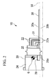
FIG. 2 is a side sectional view of the circuit board assembly shown inFIG. 1 ; -
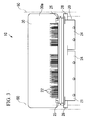
FIG. 3 is a plan view of the circuit board assembly shown inFIG. 1 ; and -
FIG. 4 is a perspective view of an electrical connector viewed from the side of being installed to a board. - The present invention will now be described in detail based on an embodiment shown in the accompanying drawings.
- As shown in
FIGS. 1 to 3 , anelectronic control device 10 includes a circuit board assembly comprising anelectrical connector 20 and acircuit board 30. - The
circuit board 30 is mounted with various electronic components, and functions as a control circuit for executing predetermined operations as an electronic control device. - The
electrical connector 20 is used to supply a power to thecircuit board 30 from the outside and to input and output electrical signals. Specifically, to theelectrical connector 20, a mating connector provided at one end of a wiring harness is connected from the outside. - The
electrical connector 20 includes a resin-madehousing 21 and a plurality ofcontacts 22 each made of a conductive material. - The
housing 21 is provided in the outer peripheral end portion of thecircuit board 30. In thehousing 21, a plate-shaped contactholding plate part 23 having holding holes for holding the plurality ofcontacts 22 is formed so as to be located in a plane orthogonally intersecting the surface of thecircuit board 30. - Each of the
contacts 22 is pressed in the holding hole so as to penetrate the contactholding plate part 23 from one side to the other side. Thecontact 22 is bent through 90 degrees with respect to the contactholding plate part 23 on thecircuit board 30 side, and oneend 22a thereof is inserted into a throughhole 31 formed in thecircuit board 30. The oneend 22a of thecontact 22 is electrically connected, by soldering, to a conductive pattern formed on the inner peripheral face of the throughhole 31 and around the circumference thereof. - Each of the
contact 22 is formed so that theother end 22b thereof extends from the contactholding plate part 23 toward the outer periphery side of thecircuit board 30 in the direction along the surface of thecircuit board 30. - The
housing 21 comprises atubular hood part 24 extending from the contactholding plate part 23 to the side on which theother ends 22b of thecontacts 22 are located. Theother ends 22b of thecontacts 22 are surrounded by thishood part 24. In this embodiment, twohood parts 24 having different sizes are provided. - Into the
hood part 24, a mating connector (male connector, not shown), which is provided at the tip end of a wiring harness, not shown, connected to an electronic control device is inserted, and, in thehood part 24, a mating contact (female contact, not shown) held to the mating connector of a wiring cord engages with theother end 22b of thecontact 22, whereby electrical connection is made. - As shown in
FIG. 4 , the contactholding plate part 23 comprises, integrally formedstopper parts 25, which abut amounting surface 30a of thecircuit board 30, on thecircuit board 30 side. Thestopper parts 25 are provided on both ends in the width direction (the direction along the surface of the circuit board 30). By thestopper parts 25, the dimension of insertion of the oneend 22a of thecontact 22 into thethrough hole 31 can be regulated. - Also, on the
housing 21, support parts (protruding parts, holding protrusions) 28 projecting toward the outside in the width direction are formed on both ends in the width direction of thehousing 21. - Each of the
support parts 28 is formed so that, in the state in which themounting surface 30a of thecircuit board 30 abuts the tip end surfaces of thestopper parts 25, a tip end surface (lower surface) 28a of thesupport part 28 is located in the same plane as asoldering surface 30b of thecircuit board 30. - As shown in
FIG. 2 , it is preferable that thesupport parts 28 be provided at positions in conformity to the gravity center position G of theelectrical connector 20 in the direction along the extending direction of theother ends 22b of thecontacts 22. - Also, the
support part 28 may be provided in plural numbers at intervals on both ends in the width direction of thehousing 21 in the direction along the extending direction of theother ends 22b of thecontacts 22. - In order to mount the above-described
electrical connector 20 to the outer peripheral portion of thecircuit board 30, first, theelectrical connector 20 is temporarily assembled to thecircuit board 30. The temporary assembling is performed as described below. Theends 22a of thecontacts 22 in theelectrical connector 20 are inserted into the throughholes 31 of thecircuit board 30, and thestopper parts 25 are abutted against themounting surface 30a of thecircuit board 30. - Next, in this state, the
ends 22a of thecontacts 22 are soldered to the conductive patterns of thecircuit board 30 by using a soldering device. - At this time, as the soldering device, a reflow-type device is used.
- The soldering device comprises support rails (support members) 50 for moving the board to be soldered while supporting it above a solder tank. Both the ends of the
circuit board 30 and thesupport parts 28 on both sides are located on these support rails 50. - The
circuit board 30 to which theelectrical connector 20 has been temporarily assembled is placed on the support rails 50, and is exposed to warm air while being moved along the support rails 50. Thereby, solder paste having been applied in advance to thecircuit board 30 is melted, and resultantly theends 22a of thecontacts 22 having been inserted into the throughholes 31 are soldered to the wiring patterns of thecircuit board 30. - When the
circuit board 30 is carried while being supported by the support rails 50 as described above, since thesupport parts 28 on both ends of theelectrical connector 20 are located on the support rails 50, theelectrical connector 20 is supported by the support rails 50. Thereby, the positional relationship between theelectrical connector 20 and thecircuit board 30 can be maintained, and in the soldering process, theelectrical connector 20 can be prevented from falling off thecircuit board 30. Therefore, theends 22a of thecontacts 22 can be soldered reliably to the wiring patterns of thecircuit board 30 so that high quality is maintained. - Also, a fastening means such as bolts or the like need not be used, and soldering can be performed reliably, so that the time and labor can be reduced, and the production efficiency can be improved. Also, a space for fastening the bolts or the like is not needed, so that the area on the
circuit board 30 can be utilized effectively. - Further, the
support parts 28 are provided at positions in conformity to the gravity center position G of theelectrical connector 20 in the direction along the extending direction of the other ends 22b of thecontacts 22, so that thecontacts 22 themselves can be carried stably. - In the above-described embodiment, a reflow-type soldering device is used. However, in place of the reflow type, a flow-type soldering device can also be used. In this case, both the ends of the
circuit board 30 and thesupport parts 28 on both sides are located on jigs (support members). The jigs are moved along the upper part of the solder tank. Then, sprayed solder in the solder tank comes into contact with thesoldering surface 30b of thecircuit board 30, and theends 22a of thecontacts 22 inserted into the throughholes 31 are soldered to the wiring patterns of thecircuit board 30. - Also, in the case of the flow type, the
tip end surface 28a of thesupport part 28 need not necessarily be formed in almost the same plane as thesoldering surface 30b of thecircuit board 30. Thetip end surface 28a has only to be formed at a height and position corresponding to a holding part formed on the jig side. - Although the
support part 28 is provided on both sides of thehousing 21, thesupport part 28 can be provided at positions other than the above-described positions. For example, thesupport part 28 can be provided at positions between thecontacts 22 arranged in plural numbers, that is, in intermediate portions or the like in the width direction of thehousing 21. - Further, in the above-described embodiment, the
housing 21 comprises thestopper parts 25, and thesestopper parts 25 abut the mountingsurface 30a of thecircuit board 30. However, thestopper parts 25 are not essential elements. The portions of theelectrical connector 20 including thehousing 21 other than theends 22a of thecontacts 22 may not be in contact with thecircuit board 30 while theends 22a of thecontacts 22 are inserted into the throughholes 31 of thecircuit board 30. In this case as well, in the soldering process, since thesupport parts 28 are supported on the soldering device side, soldering can be performed while theelectrical connector 20 is held stably. - In such a case, a space for abutting the
stopper parts 25 against the mountingsurface 30a of thecircuit board 30 is not needed, so that the area on thecircuit board 30 can be utilized further effectively. - Besides, the configurations described in the above-described embodiment can be selected, or can be changed to other configurations as appropriate without departing from the spirit and scope of the present invention.
Claims (8)
- A connector (20) provided so as to overhang from the outer peripheral portion of a circuit board (30), the connector comprising:contacts (22) electrically connected to circuit patterns of the circuit board (30); anda housing (21) for holding the contacts, whereinthe housing comprises, in a portion overhanging toward the outer periphery side from the circuit board,a holding protrusion (28), which is used to hold the housing while one end (22a) of each of the contacts is soldered to the circuit pattern of the circuit board.
- A circuit board assembly comprising:a circuit board (30); anda connector (20) according to claim 1 to which a mating connector provided at one end of an external wiring harness is connected in order to connect a circuit pattern of the circuit board (30) to the wiring harness,wherein one end (22a) of each of the contacts (22) is electrically connected to the circuit pattern of the circuit board, and the other end (22b) of each of the contacts (22) is electrically connected to a mating contact of the mating connector; andwherein in a portion overhanging toward the outer periphery side from the circuit board, the housing compises a protruding part (28) projecting toward the direction orthogonally intersecting the overhanging direction and along the surface of the circuit board.
- The circuit board assembly according to claim 2, wherein the protruding part (28) is used to hold the housing (21) while the one end (22a) of the contact is inserted into a through hole (31) formed in the circuit board (30) and is soldered to the circuit pattern of the circuit board.
- The circuit board assembly according to claim 2 or 3, wherein the protruding part (28) is provided in the vicinity of the gravity center position (G) of the connector in the overhanging direction.
- The circuit board assembly according to any one of claims 2 to 4, wherein the lower surface of the protruding part (28) is provided so as to be located in almost the same plane as the soldering surface (30b) of the circuit board (30).
- The circuit board assembly according to any one of claims 2 to 5, wherein the protruding part (28) is provided on both sides of the housing (21).
- A soldering method for a connector (20) and a circuit board (30) in which the connector described in claim 1 is used, comprising the steps of:temporarily assembling a housing (21) which holds contacts (22) to be electrically connected to circuit patterns of the circuit board (30) to the outer peripheral portion of the circuit board in a state in which the housing overhangs to the outer periphery side from the circuit board, and supporting a holding protrusion (28) formed on the housing and the circuit board on a support member (50) of a soldering device; andsoldering one end (22a) of the contact to a wiring pattern of the circuit board (30) supported on the support member.
- The soldering method according to claim 7, wherein the soldering is performed by using a reflow-type soldering device.
Applications Claiming Priority (1)
| Application Number | Priority Date | Filing Date | Title |
|---|---|---|---|
| JP2010248539A JP5550528B2 (en) | 2010-11-05 | 2010-11-05 | Circuit board assembly, connector, soldering method |
Publications (3)
| Publication Number | Publication Date |
|---|---|
| EP2451257A2 true EP2451257A2 (en) | 2012-05-09 |
| EP2451257A3 EP2451257A3 (en) | 2014-03-26 |
| EP2451257B1 EP2451257B1 (en) | 2016-07-20 |
Family
ID=44925387
Family Applications (1)
| Application Number | Title | Priority Date | Filing Date |
|---|---|---|---|
| EP11187909.4A Not-in-force EP2451257B1 (en) | 2010-11-05 | 2011-11-04 | Circuit board assembly, connector, and soldering method therefor |
Country Status (4)
| Country | Link |
|---|---|
| EP (1) | EP2451257B1 (en) |
| JP (1) | JP5550528B2 (en) |
| CN (1) | CN102544851B (en) |
| ES (1) | ES2589156T3 (en) |
Families Citing this family (1)
| Publication number | Priority date | Publication date | Assignee | Title |
|---|---|---|---|---|
| JP6398354B2 (en) * | 2014-06-13 | 2018-10-03 | ミツミ電機株式会社 | connector |
Citations (2)
| Publication number | Priority date | Publication date | Assignee | Title |
|---|---|---|---|---|
| JP2007329049A (en) | 2006-06-08 | 2007-12-20 | Denso Corp | Mounting structure for connector and mounting method therefor |
| JP2008047432A (en) | 2006-08-17 | 2008-02-28 | Tyco Electronics Amp Kk | Case of electronic control device and electric connector |
Family Cites Families (13)
| Publication number | Priority date | Publication date | Assignee | Title |
|---|---|---|---|---|
| JPH07114141B2 (en) * | 1988-09-12 | 1995-12-06 | 富士通株式会社 | Terminator card and connector soldering method |
| US5184283A (en) * | 1991-12-23 | 1993-02-02 | Ford Motor Company | Power device assembly and method |
| JP3412837B2 (en) * | 1992-06-15 | 2003-06-03 | バーグ・テクノロジー・インコーポレーテッド | Method of mounting electric connector on circuit board, electric connector for mounting on circuit board, and support member used for mounting the same |
| JPH06164117A (en) * | 1992-11-19 | 1994-06-10 | Sony Corp | Manufacture of wiring board with connector attached |
| JPH06169152A (en) * | 1992-11-30 | 1994-06-14 | Hitachi Telecom Technol Ltd | Printed wiring board structure |
| JP3006571U (en) * | 1994-07-12 | 1995-01-24 | ヒロセ電機株式会社 | Substrate connection mechanism for surface mount type electrical connector |
| JPH1051128A (en) * | 1996-08-05 | 1998-02-20 | Oki Electric Ind Co Ltd | Structure and method for mounting of surface-mounting connector as well as pc crad structure |
| US5860815A (en) * | 1997-02-21 | 1999-01-19 | Minnesota Mining And Manufacturing Company | Edge mount connector having location recesses for solder tail registration |
| JP3329230B2 (en) * | 1997-04-24 | 2002-09-30 | 松下電器産業株式会社 | Connector mounting method |
| JPH1154907A (en) * | 1997-08-04 | 1999-02-26 | Hitachi Telecom Technol Ltd | Jig for soldering printed circuit board and manufacture of printed circuit board using it |
| US6146155A (en) * | 1997-09-16 | 2000-11-14 | 3M Innovative Properties Company | Recyclable locater device for board mounted connectors |
| DE20113884U1 (en) * | 2001-08-22 | 2003-01-02 | Itt Mfg Enterprises Inc | Electrical connector for a printed circuit board |
| US7255601B2 (en) * | 2004-12-21 | 2007-08-14 | Fci Americas Technology, Inc. | Cap for an electrical connector |
-
2010
- 2010-11-05 JP JP2010248539A patent/JP5550528B2/en active Active
-
2011
- 2011-11-02 CN CN201110353062.7A patent/CN102544851B/en not_active Expired - Fee Related
- 2011-11-04 EP EP11187909.4A patent/EP2451257B1/en not_active Not-in-force
- 2011-11-04 ES ES11187909.4T patent/ES2589156T3/en active Active
Patent Citations (2)
| Publication number | Priority date | Publication date | Assignee | Title |
|---|---|---|---|---|
| JP2007329049A (en) | 2006-06-08 | 2007-12-20 | Denso Corp | Mounting structure for connector and mounting method therefor |
| JP2008047432A (en) | 2006-08-17 | 2008-02-28 | Tyco Electronics Amp Kk | Case of electronic control device and electric connector |
Also Published As
| Publication number | Publication date |
|---|---|
| ES2589156T3 (en) | 2016-11-10 |
| CN102544851A (en) | 2012-07-04 |
| JP2012099441A (en) | 2012-05-24 |
| CN102544851B (en) | 2015-10-21 |
| EP2451257B1 (en) | 2016-07-20 |
| JP5550528B2 (en) | 2014-07-16 |
| EP2451257A3 (en) | 2014-03-26 |
Similar Documents
| Publication | Publication Date | Title |
|---|---|---|
| EP2472677B1 (en) | Circuit board assembly, board device, and method for assembling a circuit board assembly | |
| US8840408B2 (en) | Crank-shaped board terminal with a protruding support portion | |
| JP2006187050A (en) | Junction block | |
| US20160192515A1 (en) | Circuit board assembly and assembling method thereof | |
| US5984698A (en) | Connector assembly having signal and ground terminals | |
| JP2015065395A (en) | Jumper module mounting circuit board and circuit board assembly | |
| JP2008091610A (en) | Printed-circuit board | |
| CN109863647B (en) | Electrical junction box | |
| US20130265731A1 (en) | Circuit board system | |
| US9553378B2 (en) | Electrical connection unit between two electronic boards | |
| US10932378B2 (en) | Connector having pins extending to more than one printed circuit board | |
| JP2017054627A (en) | Cable crimping terminal mounting body | |
| US20070111555A1 (en) | Conductor connecting module for printed circuit boards | |
| US7361060B2 (en) | Connector with bifurcated conductor | |
| EP2451257A2 (en) | Circuit board assembly, connector, and soldering method therefor | |
| JP2014229506A (en) | Terminal and electronic control unit | |
| CN211090145U (en) | Circuit board and electronic equipment | |
| JP5459195B2 (en) | Circuit assembly and electrical junction box | |
| KR20070012184A (en) | Socket for attaching electronic component and its contacting carrier | |
| EP2381751A1 (en) | Auxiliary board joining structure | |
| CN110944462A (en) | PCB (printed circuit board) welding method with metal elastic sheet switch and product | |
| CN211457577U (en) | Structural element and assembly aid for welding and fixing the same | |
| KR100577259B1 (en) | Ground terminal for ground connection between PCB and FPCB and thereof method | |
| JP2007018925A (en) | Connector device, circuit plate provided with connector device, and electronic device | |
| US8159827B2 (en) | Circuit board and method of mounting electronic component on printed board |
Legal Events
| Date | Code | Title | Description |
|---|---|---|---|
| PUAI | Public reference made under article 153(3) epc to a published international application that has entered the european phase |
Free format text: ORIGINAL CODE: 0009012 |
|
| AK | Designated contracting states |
Kind code of ref document: A2 Designated state(s): AL AT BE BG CH CY CZ DE DK EE ES FI FR GB GR HR HU IE IS IT LI LT LU LV MC MK MT NL NO PL PT RO RS SE SI SK SM TR |
|
| AX | Request for extension of the european patent |
Extension state: BA ME |
|
| PUAL | Search report despatched |
Free format text: ORIGINAL CODE: 0009013 |
|
| AK | Designated contracting states |
Kind code of ref document: A3 Designated state(s): AL AT BE BG CH CY CZ DE DK EE ES FI FR GB GR HR HU IE IS IT LI LT LU LV MC MK MT NL NO PL PT RO RS SE SI SK SM TR |
|
| AX | Request for extension of the european patent |
Extension state: BA ME |
|
| RIC1 | Information provided on ipc code assigned before grant |
Ipc: H01R 43/02 20060101ALI20140218BHEP Ipc: H05K 3/34 20060101AFI20140218BHEP Ipc: H01R 12/51 20110101ALI20140218BHEP |
|
| 17P | Request for examination filed |
Effective date: 20140919 |
|
| RBV | Designated contracting states (corrected) |
Designated state(s): AL AT BE BG CH CY CZ DE DK EE ES FI FR GB GR HR HU IE IS IT LI LT LU LV MC MK MT NL NO PL PT RO RS SE SI SK SM TR |
|
| RIC1 | Information provided on ipc code assigned before grant |
Ipc: H01R 12/72 20110101ALI20151021BHEP Ipc: H01R 4/02 20060101ALI20151021BHEP Ipc: H05K 3/34 20060101AFI20151021BHEP Ipc: H01R 12/58 20110101ALI20151021BHEP |
|
| GRAP | Despatch of communication of intention to grant a patent |
Free format text: ORIGINAL CODE: EPIDOSNIGR1 |
|
| INTG | Intention to grant announced |
Effective date: 20151208 |
|
| GRAS | Grant fee paid |
Free format text: ORIGINAL CODE: EPIDOSNIGR3 |
|
| GRAP | Despatch of communication of intention to grant a patent |
Free format text: ORIGINAL CODE: EPIDOSNIGR1 |
|
| GRAS | Grant fee paid |
Free format text: ORIGINAL CODE: EPIDOSNIGR3 |
|
| INTG | Intention to grant announced |
Effective date: 20160524 |
|
| GRAA | (expected) grant |
Free format text: ORIGINAL CODE: 0009210 |
|
| AK | Designated contracting states |
Kind code of ref document: B1 Designated state(s): AL AT BE BG CH CY CZ DE DK EE ES FI FR GB GR HR HU IE IS IT LI LT LU LV MC MK MT NL NO PL PT RO RS SE SI SK SM TR |
|
| REG | Reference to a national code |
Ref country code: GB Ref legal event code: FG4D |
|
| REG | Reference to a national code |
Ref country code: CH Ref legal event code: EP |
|
| REG | Reference to a national code |
Ref country code: IE Ref legal event code: FG4D |
|
| REG | Reference to a national code |
Ref country code: AT Ref legal event code: REF Ref document number: 814997 Country of ref document: AT Kind code of ref document: T Effective date: 20160815 |
|
| REG | Reference to a national code |
Ref country code: DE Ref legal event code: R096 Ref document number: 602011028289 Country of ref document: DE |
|
| REG | Reference to a national code |
Ref country code: ES Ref legal event code: FG2A Ref document number: 2589156 Country of ref document: ES Kind code of ref document: T3 Effective date: 20161110 Ref country code: LT Ref legal event code: MG4D |
|
| REG | Reference to a national code |
Ref country code: NL Ref legal event code: MP Effective date: 20160720 Ref country code: FR Ref legal event code: PLFP Year of fee payment: 6 |
|
| REG | Reference to a national code |
Ref country code: AT Ref legal event code: MK05 Ref document number: 814997 Country of ref document: AT Kind code of ref document: T Effective date: 20160720 |
|
| PG25 | Lapsed in a contracting state [announced via postgrant information from national office to epo] |
Ref country code: NL Free format text: LAPSE BECAUSE OF FAILURE TO SUBMIT A TRANSLATION OF THE DESCRIPTION OR TO PAY THE FEE WITHIN THE PRESCRIBED TIME-LIMIT Effective date: 20160720 Ref country code: IS Free format text: LAPSE BECAUSE OF FAILURE TO SUBMIT A TRANSLATION OF THE DESCRIPTION OR TO PAY THE FEE WITHIN THE PRESCRIBED TIME-LIMIT Effective date: 20161120 Ref country code: LT Free format text: LAPSE BECAUSE OF FAILURE TO SUBMIT A TRANSLATION OF THE DESCRIPTION OR TO PAY THE FEE WITHIN THE PRESCRIBED TIME-LIMIT Effective date: 20160720 Ref country code: NO Free format text: LAPSE BECAUSE OF FAILURE TO SUBMIT A TRANSLATION OF THE DESCRIPTION OR TO PAY THE FEE WITHIN THE PRESCRIBED TIME-LIMIT Effective date: 20161020 Ref country code: IT Free format text: LAPSE BECAUSE OF FAILURE TO SUBMIT A TRANSLATION OF THE DESCRIPTION OR TO PAY THE FEE WITHIN THE PRESCRIBED TIME-LIMIT Effective date: 20160720 Ref country code: RS Free format text: LAPSE BECAUSE OF FAILURE TO SUBMIT A TRANSLATION OF THE DESCRIPTION OR TO PAY THE FEE WITHIN THE PRESCRIBED TIME-LIMIT Effective date: 20160720 Ref country code: HR Free format text: LAPSE BECAUSE OF FAILURE TO SUBMIT A TRANSLATION OF THE DESCRIPTION OR TO PAY THE FEE WITHIN THE PRESCRIBED TIME-LIMIT Effective date: 20160720 Ref country code: FI Free format text: LAPSE BECAUSE OF FAILURE TO SUBMIT A TRANSLATION OF THE DESCRIPTION OR TO PAY THE FEE WITHIN THE PRESCRIBED TIME-LIMIT Effective date: 20160720 |
|
| PG25 | Lapsed in a contracting state [announced via postgrant information from national office to epo] |
Ref country code: GR Free format text: LAPSE BECAUSE OF FAILURE TO SUBMIT A TRANSLATION OF THE DESCRIPTION OR TO PAY THE FEE WITHIN THE PRESCRIBED TIME-LIMIT Effective date: 20161021 Ref country code: SE Free format text: LAPSE BECAUSE OF FAILURE TO SUBMIT A TRANSLATION OF THE DESCRIPTION OR TO PAY THE FEE WITHIN THE PRESCRIBED TIME-LIMIT Effective date: 20160720 Ref country code: PL Free format text: LAPSE BECAUSE OF FAILURE TO SUBMIT A TRANSLATION OF THE DESCRIPTION OR TO PAY THE FEE WITHIN THE PRESCRIBED TIME-LIMIT Effective date: 20160720 Ref country code: BE Free format text: LAPSE BECAUSE OF NON-PAYMENT OF DUE FEES Effective date: 20160720 Ref country code: AT Free format text: LAPSE BECAUSE OF FAILURE TO SUBMIT A TRANSLATION OF THE DESCRIPTION OR TO PAY THE FEE WITHIN THE PRESCRIBED TIME-LIMIT Effective date: 20160720 Ref country code: LV Free format text: LAPSE BECAUSE OF FAILURE TO SUBMIT A TRANSLATION OF THE DESCRIPTION OR TO PAY THE FEE WITHIN THE PRESCRIBED TIME-LIMIT Effective date: 20160720 Ref country code: PT Free format text: LAPSE BECAUSE OF FAILURE TO SUBMIT A TRANSLATION OF THE DESCRIPTION OR TO PAY THE FEE WITHIN THE PRESCRIBED TIME-LIMIT Effective date: 20161121 |
|
| REG | Reference to a national code |
Ref country code: DE Ref legal event code: R097 Ref document number: 602011028289 Country of ref document: DE |
|
| PG25 | Lapsed in a contracting state [announced via postgrant information from national office to epo] |
Ref country code: EE Free format text: LAPSE BECAUSE OF FAILURE TO SUBMIT A TRANSLATION OF THE DESCRIPTION OR TO PAY THE FEE WITHIN THE PRESCRIBED TIME-LIMIT Effective date: 20160720 Ref country code: RO Free format text: LAPSE BECAUSE OF FAILURE TO SUBMIT A TRANSLATION OF THE DESCRIPTION OR TO PAY THE FEE WITHIN THE PRESCRIBED TIME-LIMIT Effective date: 20160720 |
|
| PLBE | No opposition filed within time limit |
Free format text: ORIGINAL CODE: 0009261 |
|
| STAA | Information on the status of an ep patent application or granted ep patent |
Free format text: STATUS: NO OPPOSITION FILED WITHIN TIME LIMIT |
|
| PG25 | Lapsed in a contracting state [announced via postgrant information from national office to epo] |
Ref country code: SM Free format text: LAPSE BECAUSE OF FAILURE TO SUBMIT A TRANSLATION OF THE DESCRIPTION OR TO PAY THE FEE WITHIN THE PRESCRIBED TIME-LIMIT Effective date: 20160720 Ref country code: DK Free format text: LAPSE BECAUSE OF FAILURE TO SUBMIT A TRANSLATION OF THE DESCRIPTION OR TO PAY THE FEE WITHIN THE PRESCRIBED TIME-LIMIT Effective date: 20160720 Ref country code: BG Free format text: LAPSE BECAUSE OF FAILURE TO SUBMIT A TRANSLATION OF THE DESCRIPTION OR TO PAY THE FEE WITHIN THE PRESCRIBED TIME-LIMIT Effective date: 20161020 Ref country code: SK Free format text: LAPSE BECAUSE OF FAILURE TO SUBMIT A TRANSLATION OF THE DESCRIPTION OR TO PAY THE FEE WITHIN THE PRESCRIBED TIME-LIMIT Effective date: 20160720 Ref country code: CZ Free format text: LAPSE BECAUSE OF FAILURE TO SUBMIT A TRANSLATION OF THE DESCRIPTION OR TO PAY THE FEE WITHIN THE PRESCRIBED TIME-LIMIT Effective date: 20160720 |
|
| 26N | No opposition filed |
Effective date: 20170421 |
|
| REG | Reference to a national code |
Ref country code: CH Ref legal event code: PL |
|
| REG | Reference to a national code |
Ref country code: DE Ref legal event code: R082 Ref document number: 602011028289 Country of ref document: DE Representative=s name: SCHMITT-NILSON SCHRAUD WAIBEL WOHLFROM PATENTA, DE |
|
| GBPC | Gb: european patent ceased through non-payment of renewal fee |
Effective date: 20161104 |
|
| PG25 | Lapsed in a contracting state [announced via postgrant information from national office to epo] |
Ref country code: LI Free format text: LAPSE BECAUSE OF NON-PAYMENT OF DUE FEES Effective date: 20161130 Ref country code: CH Free format text: LAPSE BECAUSE OF NON-PAYMENT OF DUE FEES Effective date: 20161130 |
|
| REG | Reference to a national code |
Ref country code: IE Ref legal event code: MM4A |
|
| PG25 | Lapsed in a contracting state [announced via postgrant information from national office to epo] |
Ref country code: SI Free format text: LAPSE BECAUSE OF FAILURE TO SUBMIT A TRANSLATION OF THE DESCRIPTION OR TO PAY THE FEE WITHIN THE PRESCRIBED TIME-LIMIT Effective date: 20160720 |
|
| PG25 | Lapsed in a contracting state [announced via postgrant information from national office to epo] |
Ref country code: LU Free format text: LAPSE BECAUSE OF NON-PAYMENT OF DUE FEES Effective date: 20161130 |
|
| REG | Reference to a national code |
Ref country code: FR Ref legal event code: PLFP Year of fee payment: 7 |
|
| PG25 | Lapsed in a contracting state [announced via postgrant information from national office to epo] |
Ref country code: IE Free format text: LAPSE BECAUSE OF NON-PAYMENT OF DUE FEES Effective date: 20161104 Ref country code: GB Free format text: LAPSE BECAUSE OF NON-PAYMENT OF DUE FEES Effective date: 20161104 |
|
| PG25 | Lapsed in a contracting state [announced via postgrant information from national office to epo] |
Ref country code: HU Free format text: LAPSE BECAUSE OF FAILURE TO SUBMIT A TRANSLATION OF THE DESCRIPTION OR TO PAY THE FEE WITHIN THE PRESCRIBED TIME-LIMIT; INVALID AB INITIO Effective date: 20111104 Ref country code: CY Free format text: LAPSE BECAUSE OF FAILURE TO SUBMIT A TRANSLATION OF THE DESCRIPTION OR TO PAY THE FEE WITHIN THE PRESCRIBED TIME-LIMIT Effective date: 20160720 |
|
| PG25 | Lapsed in a contracting state [announced via postgrant information from national office to epo] |
Ref country code: TR Free format text: LAPSE BECAUSE OF FAILURE TO SUBMIT A TRANSLATION OF THE DESCRIPTION OR TO PAY THE FEE WITHIN THE PRESCRIBED TIME-LIMIT Effective date: 20160720 Ref country code: MC Free format text: LAPSE BECAUSE OF FAILURE TO SUBMIT A TRANSLATION OF THE DESCRIPTION OR TO PAY THE FEE WITHIN THE PRESCRIBED TIME-LIMIT Effective date: 20160720 Ref country code: MK Free format text: LAPSE BECAUSE OF FAILURE TO SUBMIT A TRANSLATION OF THE DESCRIPTION OR TO PAY THE FEE WITHIN THE PRESCRIBED TIME-LIMIT Effective date: 20160720 |
|
| REG | Reference to a national code |
Ref country code: FR Ref legal event code: PLFP Year of fee payment: 8 |
|
| PG25 | Lapsed in a contracting state [announced via postgrant information from national office to epo] |
Ref country code: MT Free format text: LAPSE BECAUSE OF NON-PAYMENT OF DUE FEES Effective date: 20161104 |
|
| PG25 | Lapsed in a contracting state [announced via postgrant information from national office to epo] |
Ref country code: AL Free format text: LAPSE BECAUSE OF FAILURE TO SUBMIT A TRANSLATION OF THE DESCRIPTION OR TO PAY THE FEE WITHIN THE PRESCRIBED TIME-LIMIT Effective date: 20160720 |
|
| PGFP | Annual fee paid to national office [announced via postgrant information from national office to epo] |
Ref country code: FR Payment date: 20190913 Year of fee payment: 9 |
|
| PGFP | Annual fee paid to national office [announced via postgrant information from national office to epo] |
Ref country code: ES Payment date: 20191202 Year of fee payment: 9 |
|
| PGFP | Annual fee paid to national office [announced via postgrant information from national office to epo] |
Ref country code: DE Payment date: 20201020 Year of fee payment: 10 |
|
| PG25 | Lapsed in a contracting state [announced via postgrant information from national office to epo] |
Ref country code: FR Free format text: LAPSE BECAUSE OF NON-PAYMENT OF DUE FEES Effective date: 20201130 |
|
| REG | Reference to a national code |
Ref country code: ES Ref legal event code: FD2A Effective date: 20220131 |
|
| PG25 | Lapsed in a contracting state [announced via postgrant information from national office to epo] |
Ref country code: ES Free format text: LAPSE BECAUSE OF NON-PAYMENT OF DUE FEES Effective date: 20201105 |
|
| REG | Reference to a national code |
Ref country code: DE Ref legal event code: R119 Ref document number: 602011028289 Country of ref document: DE |
|
| PG25 | Lapsed in a contracting state [announced via postgrant information from national office to epo] |
Ref country code: DE Free format text: LAPSE BECAUSE OF NON-PAYMENT OF DUE FEES Effective date: 20220601 |