EP2450952A2 - Leistungshalbleitermodul mit einem Substrat mit einer Mehrzahl gleichartig ausgebildeter Leiterbahngruppen - Google Patents
Leistungshalbleitermodul mit einem Substrat mit einer Mehrzahl gleichartig ausgebildeter Leiterbahngruppen Download PDFInfo
- Publication number
- EP2450952A2 EP2450952A2 EP20110183244 EP11183244A EP2450952A2 EP 2450952 A2 EP2450952 A2 EP 2450952A2 EP 20110183244 EP20110183244 EP 20110183244 EP 11183244 A EP11183244 A EP 11183244A EP 2450952 A2 EP2450952 A2 EP 2450952A2
- Authority
- EP
- European Patent Office
- Prior art keywords
- power semiconductor
- semiconductor module
- substrate
- module according
- load connection
- Prior art date
- Legal status (The legal status is an assumption and is not a legal conclusion. Google has not performed a legal analysis and makes no representation as to the accuracy of the status listed.)
- Granted
Links
Images


Classifications
-
- H—ELECTRICITY
- H10—SEMICONDUCTOR DEVICES; ELECTRIC SOLID-STATE DEVICES NOT OTHERWISE PROVIDED FOR
- H10W—GENERIC PACKAGES, INTERCONNECTIONS, CONNECTORS OR OTHER CONSTRUCTIONAL DETAILS OF DEVICES COVERED BY CLASS H10
- H10W90/00—Package configurations
-
- H—ELECTRICITY
- H10—SEMICONDUCTOR DEVICES; ELECTRIC SOLID-STATE DEVICES NOT OTHERWISE PROVIDED FOR
- H10W—GENERIC PACKAGES, INTERCONNECTIONS, CONNECTORS OR OTHER CONSTRUCTIONAL DETAILS OF DEVICES COVERED BY CLASS H10
- H10W40/00—Arrangements for thermal protection or thermal control
- H10W40/20—Arrangements for cooling
- H10W40/25—Arrangements for cooling characterised by their materials
- H10W40/255—Arrangements for cooling characterised by their materials having a laminate or multilayered structure, e.g. direct bond copper [DBC] ceramic substrates
-
- H—ELECTRICITY
- H10—SEMICONDUCTOR DEVICES; ELECTRIC SOLID-STATE DEVICES NOT OTHERWISE PROVIDED FOR
- H10W—GENERIC PACKAGES, INTERCONNECTIONS, CONNECTORS OR OTHER CONSTRUCTIONAL DETAILS OF DEVICES COVERED BY CLASS H10
- H10W44/00—Electrical arrangements for controlling or matching impedance
- H10W44/501—Inductive arrangements
-
- H—ELECTRICITY
- H10—SEMICONDUCTOR DEVICES; ELECTRIC SOLID-STATE DEVICES NOT OTHERWISE PROVIDED FOR
- H10W—GENERIC PACKAGES, INTERCONNECTIONS, CONNECTORS OR OTHER CONSTRUCTIONAL DETAILS OF DEVICES COVERED BY CLASS H10
- H10W70/00—Package substrates; Interposers; Redistribution layers [RDL]
- H10W70/60—Insulating or insulated package substrates; Interposers; Redistribution layers
- H10W70/62—Insulating or insulated package substrates; Interposers; Redistribution layers characterised by their interconnections
- H10W70/65—Shapes or dispositions of interconnections
-
- H—ELECTRICITY
- H10—SEMICONDUCTOR DEVICES; ELECTRIC SOLID-STATE DEVICES NOT OTHERWISE PROVIDED FOR
- H10W—GENERIC PACKAGES, INTERCONNECTIONS, CONNECTORS OR OTHER CONSTRUCTIONAL DETAILS OF DEVICES COVERED BY CLASS H10
- H10W72/00—Interconnections or connectors in packages
- H10W72/50—Bond wires
- H10W72/531—Shapes of wire connectors
- H10W72/5363—Shapes of wire connectors the connected ends being wedge-shaped
-
- H—ELECTRICITY
- H10—SEMICONDUCTOR DEVICES; ELECTRIC SOLID-STATE DEVICES NOT OTHERWISE PROVIDED FOR
- H10W—GENERIC PACKAGES, INTERCONNECTIONS, CONNECTORS OR OTHER CONSTRUCTIONAL DETAILS OF DEVICES COVERED BY CLASS H10
- H10W72/00—Interconnections or connectors in packages
- H10W72/50—Bond wires
- H10W72/541—Dispositions of bond wires
- H10W72/547—Dispositions of multiple bond wires
- H10W72/5473—Dispositions of multiple bond wires multiple bond wires connected to a common bond pad
-
- H—ELECTRICITY
- H10—SEMICONDUCTOR DEVICES; ELECTRIC SOLID-STATE DEVICES NOT OTHERWISE PROVIDED FOR
- H10W—GENERIC PACKAGES, INTERCONNECTIONS, CONNECTORS OR OTHER CONSTRUCTIONAL DETAILS OF DEVICES COVERED BY CLASS H10
- H10W90/00—Package configurations
- H10W90/701—Package configurations characterised by the relative positions of pads or connectors relative to package parts
- H10W90/751—Package configurations characterised by the relative positions of pads or connectors relative to package parts of bond wires
- H10W90/753—Package configurations characterised by the relative positions of pads or connectors relative to package parts of bond wires between laterally-adjacent chips
-
- H—ELECTRICITY
- H10—SEMICONDUCTOR DEVICES; ELECTRIC SOLID-STATE DEVICES NOT OTHERWISE PROVIDED FOR
- H10W—GENERIC PACKAGES, INTERCONNECTIONS, CONNECTORS OR OTHER CONSTRUCTIONAL DETAILS OF DEVICES COVERED BY CLASS H10
- H10W90/00—Package configurations
- H10W90/701—Package configurations characterised by the relative positions of pads or connectors relative to package parts
- H10W90/751—Package configurations characterised by the relative positions of pads or connectors relative to package parts of bond wires
- H10W90/754—Package configurations characterised by the relative positions of pads or connectors relative to package parts of bond wires between a chip and a stacked insulating package substrate, interposer or RDL
Definitions
- the invention describes a power semiconductor module having at least one substrate, arranged on conductor tracks of this substrate Power semiconductor components and circuit-compatible connection devices.
- Such power semiconductor modules have, according to the generally known prior art, a multiplicity of different circuit topologies.
- the best known are half-bridge circuits with two power switches or rectifier circuits with power diodes and / or power thyristors.
- Such power semiconductor module has a base plate and disposed thereon a plurality of Subtraten, wherein on each substrate printed conductors for the circuit arrangement of power semiconductor components are provided.
- this power semiconductor module has load connection elements that contact the substrate and have external connection devices. These load connection elements are designed such that they run in a substantial portion closely adjacent to each other in order to minimize unwanted parasitic inductances.
- the power semiconductor module without base plate and to connect the load connection elements by a pressure device electrically conductive to the substrate.
- the band-like load connection elements on individual contact feet which protrude through recesses of the housing to the substrate.
- the load connection element are arranged in a substantial portion parallel and closely adjacent to each other.
- the object of the invention is to present a power semiconductor module which, in a compact design, enables efficient heat emission to a cooling device and has an efficient internal current conduction with low parasitic inductances.
- the power semiconductor module according to the invention has at least one substrate for direct arrangement on a heat sink or for arrangement on a preferably metallic base plate.
- the substrate forms the circuit carrier of the power electronic circuit of the power semiconductor module.
- the substrate is covered by a plastic housing, which also encloses the other internal components of the power semiconductor module and electrically isolated from contact.
- the substrate itself is preferably designed in such a way that its side facing away from the interior of the power semiconductor module is electrically isolated from the internal circuit and only the heat dissipation to a cooling device is used.
- copper-clad substrates are particularly preferred on both sides, wherein the interior of the power semiconductor module facing copper cladding is structured in itself and thus forms the tracks of the circuit.
- the outer Kupferkaschtechnik primarily serves the efficient heat dissipation and thus forms an outer side, usually the base of the power semiconductor module.
- the power semiconductor module according to the invention has on the at least one substrate a plurality of interconnect groups arranged concentrically around a center of this substrate.
- a trace group a Arrangement of at least two tracks to guide different potential understood.
- At least two of these interconnects different potential of a common interconnect group at least one power semiconductor device is provided in each case.
- the half-bridge circuit two tracks with the DC potentials of different sign and a further track with AC potential are provided.
- a first semiconductor switch preferably formed from an anti-parallel circuit of bipolar power transistors and power diodes, is in this case arranged on the conductor positive DC voltage potential, a second semiconductor switch on the conductor with alternating potential.
- the circuit-compatible connections for the formation of the half-bridge circuit are formed by means of module-internal connection devices, configured as an example by wire bonds.
- the substrate is designed like a disk with a circular base surface, and the conductor track groups form circular sectors of this substrate. It is particularly preferred if exactly three, a small multiple of two or exactly five circular sectors are provided. This embodiment achieves a particularly compact design of the power semiconductor module.
- the conductor tracks of a circular sector that is to say a track group on which the power semiconductor components are arranged, are designed as radially successive sector segments.
- the power semiconductor components of the respective sector segments are cooled particularly effectively.
- the power semiconductor module has load connection elements assigned to the potentials of the substrate, each of which has a main body and at least one contact element. At least two, preferably those of the positive and negative DC potential, this body of the Load connection elements are arranged concentrically to one another and to the center of the substrate. Moreover, it is preferred if the respective base body is cylindrically symmetrical, preferably designed as a hollow cylinder. As a result of this inner current flow in the closely adjacent base body, the parasitic inductances produced by the current flow, for example during the commutation phase of a half-bridge, are particularly low. This also enables efficient current conduction of high current carrying capacity.
- each load connection element is preferably formed integrally with the base body and electrically connects the load connection element with an associated conductor track or with at least one power semiconductor component arranged on a conductor track.
- each load connection element has an external connection device, which consists of a part of the load connection element itself and of a contact device, for example in the form of a screw connection.
- the substrate has a central recess.
- the load connection elements specifically their contact elements
- a pressure-introducing device of the pressure device reaching through the central recess, it is possible to initiate the pressure force on the load connection elements and thus their non-positive contact symmetrically with respect to the center.
- This is particularly preferred for the uniform cooling of the substrate and the power semiconductor components arranged thereon via a providable cooling device.
- a cohesive connection for example by means of soldering or pressure sintering, can also be advantageous.
- Fig. 1 schematically shows a half-bridge circuit.
- Fig. 2 shows a first embodiment of a power semiconductor module according to the invention in plan view.
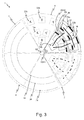
- Fig. 3 shows a second embodiment of a power semiconductor module according to the invention in plan view.
- Fig. 4 shows the second embodiment in cross section.
- Fig. 1 schematically shows a half-bridge circuit having a first and a second power switch (12, 22), which is in each case as a bipolar transistor (12a, 22a) with an antiparallel-connected diode (12b, 22b) is formed.
- a bipolar transistor (12a, 22a) with an antiparallel-connected diode (12b, 22b) is formed.
- the first power switch (12) is connected in this circuit topology between the positive DC potential and the AC potential, the output of the circuit.
- the second power switch (22) is connected between the alternating potential and the negative DC potential.
- Fig. 2 shows a first embodiment of a power semiconductor module (1) according to the invention with a circuit topology of a half-bridge circuit, cf. Fig. 1 , in top view.
- the power semiconductor module (1) here has a substrate (2) with five conductor track groups (4) indicated by dotted lines, although not all details are shown in each track group.
- the substrate (2) is in this case formed as a disk-shaped industrial ceramic, on which the conductor tracks (10, 20, 30) of the conductor track groups (4) are formed as Kupferkaschtechniken.
- Each track group (4) forms a circular sector, each of the five circular sectors being basically similar, i. is formed in the same geometric configuration.
- the five circular sectors are arranged rotated against each other and thus form a complete circle.
- Each interconnect group (4) consists in turn of three interconnects (10, 20, 30) of different potential, wherein in a first sector segment (41) of the interconnect group (4), which adjoins directly to the center of the substrate (2), that interconnect ( 10) is arranged with a positive DC potential.
- a radially subsequent sector segment (42) the conductor track (20) is arranged with alternating potential, while the side of the two radially successive sector segments (41, 42) in a further sector segment (43) that conductor track (30) is arranged with a negative DC potential.
- a first power switch (12) On the conductor track (10) with a positive DC potential, a first power switch (12), see. Fig. 1 , in an embodiment of two bipolar power transistors (12a) connected in parallel, and a power diode (12b) connected in antiparallel thereto.
- a second power switch (22) On the conductor track (20) with AC potential is a second power switch (22), see. Fig. 1 , arranged in the same configuration as the first one.
- a plurality of wire bond connections (84), which are only indicated, are present as the module-internal connection device.
- the substrate (2) is thus cylindrically symmetrical about a straight line formed by its center.
- This embodiment is particularly suitable for providing load connection elements (50, 60, 70), which are all arranged concentrically around the center of the substrate (2).
- these load connection elements (50, 60, 70) each have a base body (52, 62, 72), which is designed as a hollow cylinder.
- the positions of the respective hollow cylinders are represented by the dot-dash lines (14, 24, 34).
- Each of these load connection elements (50, 60, 70) furthermore has at least one contact element (54, 64, 74) which is electrically conductively connected to an associated contact surface (16, 26, 36) of the associated conductor track (10, 20, 30) ,
- Fig. 3 shows a second embodiment of a power semiconductor module according to the invention (1) in plan view and analog representation Fig. 2 , while Fig. 4 shows this second embodiment in cross section.
- This power semiconductor module (1) in turn has a disk-shaped substrate (2) with a circular base. Even square or rectangular bases are quite conceivable.
- the substrate (2) has in this embodiment, six conductor track groups (4), which are formed as circular sectors, as indicated by the dotted lines.
- Each of these conductor track groups (4) consists of two radially successive sector segments (41, 42) with approximately the same surface area, whereby the power loss of the power semiconductor components (12 a / b, 22 a / b) in the form of waste heat is distributed in each case on the same surface and in a on the underside of the substrate (2) can be dispensed cooling device.
- This is also the Kupferkaschtechnik (8) on the inside of the power semiconductor module (1) facing away from the substrate (2), which incidentally consists of a disc-shaped industrial ceramic (6), such as alumina.
- a copper lamination which is structured in itself, is likewise provided, which forms the conductor tracks (10, 20, 30).
- Each of the six conductor track groups (4) is identical in its basic geometric configuration, but these are each formed rotated by 60 ° to each other and arranged on the disc-shaped substrate (2).
- the respective interconnect group (4) consists here only of two interconnects (10, 20), one with positive DC potential and one with AC potential, with a respective circuit breaker (12, 22), cf. Fig. 1 formed with two bipolar transistors (12a, 22a) and a power diode (12b, 22b) is arranged.
- the circuit-compatible connection of this Power semiconductor components (12 a / b, 22 a / b) takes place by way of example again by means of wire bond connections (84), whereby of course other internal connecting devices are providable and possibly advantageous.
- the load connection elements (50, 60, 70) are basically identical to those according to FIG Fig. 2 formed and have a designed as a hollow cylinder base body (52, 62, 72) facing the substrate (2) each having at least one contact element (54, 64, 74).
- the load connection elements (50, 60) assigned to the positive direct current potential and the alternating current potential each have a plurality of contact devices (52, 62) which are electrically conductively connected to contact surfaces (16, 26) of the associated conductor tracks (10, 20).
- the load connection element (70) assigned to the negative direct-current potential likewise has a plurality of contact devices (72) which, however, are each electrically connected to a contact surface (38) of the power semiconductor components (22 a / b) arranged on the conductor path (20) with alternating voltage potential ,
- these power semiconductor components (22 a / b) have a particularly suitably configured surface, for example in the form of a particularly thick contact metal layer.
- the main bodies (52, 72) of the load connection elements (50, 70) assigned to the DC potentials are arranged concentrically around the center of the substrate (2) and closely adjacent to one another.
- the contact devices (52, 72) of both load connection elements (50, 70) are bent here, this offset being provided near the substrate (2) in order to encompass the area around the current between the load connection elements (50, FIG. 70) and thus to keep the parasitic inductances small.
- the contact elements (62) of the AC voltage potential associated load connection element (60) are formed here without such cranking.
- each formed as a hollow cylinder body (52, 62, 72) is basically arbitrary within wide limits and is in most advantageous cases significantly less than the radius of the substrate (2).
- the respective load connection elements (50, 60, 70) furthermore have external connection devices (56, 66, 76), which are formed here by way of example as sections that are connected in one piece to the base body (52, 62, 72) and parallel to the substrate (2). These sections each have a recess for the passage of a screw (58, 68, 78) for connection to a screw receptacle, which may be arranged by way of example in a housing, not shown, on.
- Other connection variants are of course alternatively providable.
- the electrically conductive connection of the contact devices (52, 62, 72) of the load connection elements (50, 60, 70) with the contact surfaces (16, 26) of the conductor tracks (10, 20) or with contact surfaces (38) of power semiconductor components (22 a / b) may be formed by means of cohesive methods. In the illustrated embodiment, this connection is formed by means of a non-positive process.
- the power semiconductor module to a printing device (80), which on the Load connection elements (50, 60, 70) in the direction of the substrate (2) initiates pressure.
Landscapes
- Rectifiers (AREA)
- Power Conversion In General (AREA)
- Cooling Or The Like Of Semiconductors Or Solid State Devices (AREA)
Abstract
Description
- Die Erfindung beschreibt ein Leistungshalbleitermodul mit mindestens einem Substrat, auf Leiterbahnen dieses Substrats angeordneten
Leistungshalbleiterbauelementen und schaltungsgerechten Verbindungseinrichtungen. Derartige Leistungshalbleitermodule weisen gemäß dem allgemein bekannten Stand der Technik eine Vielzahl verschiedener Schaltungstopologien auf. Die bekanntesten sind Halbbrückenschaltungen mit zwei Leistungsschaltern oder Gleichrichterschaltungen mit Leistungsdioden und / oder Leistungsthyristoren. - Aus der nicht vorveröffentlichten
DE 10 2009 037 257 A1 ist beispielhaft ein
derartiges Leistungshalbleitermodul bekannt. Dieses weist ein Grundplatte und auf dieser angeordnet eine Mehrzahl von Subtraten auf, wobei auf jedem Substrat Leiterbahnen zur schaltungsgerechten Anordnung von Leistungshalbleiterbauelementen vorgesehen sind. Zudem weist dieses Leistungshalbleitermodul Lastanschlusselemente auf, die das Substrat kontaktieren und externe Verbindungseinrichtungen aufweisen. Diese Lastanschlusselemente sind derart ausgebildet, dass sie in einem wesentlichen Abschnitt eng benachbart zueinander verlaufen, um unerwünschte parasitäre Induktivitäten möglichst gering zu halten. - Beispielhaft aus der
DE 10 2006 006 425 A1 ist es weiterhin bekannt, das Leistungshalbleitermodul ohne Grundplatte auszubilden und die Lastanschlusselemente durch eine Druckeinrichtung elektrisch leitend mit dem Substrat zu verbinden. Hierzu weisen die bandartig ausgebildeten Lastanschlusselemente einzelne Kontaktfüße auf, die durch Ausnehmungen des Gehäuses zum Substrat hindurchragen. Auch bei dieser Ausgestaltung sind die Lastanschlusselement in einem wesentlichen Abschnitt parallel und eng benachbart zueinander angeordnet. - Der Erfindung liegt die Aufgabe zugrunde ein Leistungshalbleitermodul vorzustellen, das bei einem kompakten Aufbau eine effiziente Wärmeabgabe zu einer Kühleinrichtung ermöglicht und eine effiziente, mit geringen parasitäten Induktivitäten behaftete interne Stromführung aufweist.
- Die Aufgabe wird erfindungsgemäß gelöst durch ein Leistungshalbleitermodul mit den Merkmalen des Anspruchs 1. Bevorzugte Ausführungsformen sind in den abhängigen Ansprüchen beschrieben.
- Das erfindungsgemäße Leistungshalbleitermodul weist mindestens ein Substrat zur direkten Anordnung auf einem Kühlkörper oder zur Anordnung auf einer vorzugsweise metallischen Grundplatte auf. Das Substrat bildet den Schaltungsträger der leistungselektronischen Schaltung des Leistungshalbleitermoduls aus. Vorzugsweise ist das Substrat von einem Kunststoffgehäuse überdeckt, das auch die weiteren internen Komponenten des Leistungshalbleitermoduls umschließt und elektrisch gegen Berührung isoliert.
- Das Substrat selbst ist in bevorzugter Weise derart ausgebildet, dass seine dem Inneren des Leistungshalbleitermoduls abgewandte Seite elektrisch von der internen Schaltung isoliert ist und nur der Wärmeabfuhr zu einer Kühleinrichtung dient. Für diese Ausgestaltung sind besonders beidseitig kupferkaschierte Substrate bevorzugt, wobei die dem Inneren des Leistungshalbleitermoduls zugewandte Kupferkaschierung in sich strukturiert ist und so die Leiterbahnen der Schaltung ausbildet. Die äußere Kupferkaschierung dient vornehmlich der effizienten Wärmeabgabe und bildet somit eine Außenseite, meist die Grundfläche, des Leistungshalbleitermoduls aus.
- Das erfindungsgemäße Leistungshalbleitermodul weist auf dem mindestens einen Substrat eine Mehrzahl von konzentrisch um einen Mittelpunkt dieses Substrats angeordneten Leiterbahngruppen auf. Hierbei wird unter einer Leiterbahngruppe eine Anordnung von mindestens zwei Leiterbahnen zur Führung unterschiedlichen Potentials verstanden.
- Auf mindestens zwei dieser Leiterbahnen unterschiedlichen Potentials einer gemeinsamen Leiterbahngruppe ist jeweils mindestens ein Leistungshalbleiterbauelement vorgesehen. Beispielhaft im Fall der Halbbrückenschaltung sind zwei Leiterbahnen mit den Gleichspannungspotentialen unterschiedlichen Vorzeichens und eine weitere Leiterbahn mit Wechselspannungspotential vorgesehen. Ein erster Halbleiterschalter, vorzugsweise ausgebildet aus einer Antiparallelschaltung von bipolaren Leistungstransistoren und Leistungsdioden, ist hierbei auf der Leiterbahn positiven Gleichspannungspotentials angeordnet, ein zweiter Halbleiterschalter auf der Leiterbahn mit Wechselpotential. Die schaltungsgerechten Verbindungen zur Ausbildung der Halbbrückenschaltung sind mittels modulinterner Verbindungseinrichtungen, beispielhaft ausgestaltet als Drahtbondverbindungen, ausgebildet.
- Alternativ sind selbstverständlich auch andere Leistungshalbleiterbauelemente wie Thyristoren oder Feldeffektransistoren vorsehbar, wodurch auch fast beliebige andere Schaltungstopologien verwirklicht werden können.
- Es ist weiterhin bevorzugt, wenn das Substrat scheibenfömig mit einer kreisförmigen Grundfläche ausgebildet ist, und die Leiterbahngruppen Kreissektoren dieses Substrats bilden. Hierbei ist es besonders bevorzugt, wenn genau drei, ein kleines Vielfaches von zwei oder genau fünf Kreissektoren vorgesehen sind. Durch diese Ausgestaltung wird ein besonders kompakter Aufbau des Leistungshalbleitermoduls erreicht.
- Weiterhin ist es vorteilhaft, wenn alle Leiterbahngruppen gleichartig, in gleicher geometrischer Ausgestaltung ausgebildet und gegeneinander verdreht angeordnet sind. Hierzu sind beispielhaft die Leiterbahnen eines Kreissektors, also einer Leitbahngruppe, auf denen die Leistungshalbleiterbauelemente angeordnet sind als radial aufeinander folgende Sektorsegmente ausgebildet. Hierbei werden die Leistungshalbleiterbauelemente der jeweiligen Sektorsegmente besonders wirksam gekühlt.
- Weiterhin weist das Leistungshalbleitermodul den Potentialen des Substrats zugeordnete Lastanschlusselemente auf, die jeweils einen Grundkörper und mindestens ein Kontaktelement aufweisen. Mindestens zwei, vorzugsweise diejenigen des positiven und des negativen Gleichspannungspotentials, dieser Grundkörper der Lastanschlusselemente sind konzentrisch zueinander und zu dem Mittelpunkt des Substrats angeordnet. Darüber hinaus ist es bevorzugt, wenn der jeweilige Grundkörper zylindersymmetrisch, vorzugsweise als Hohlzylinder, ausgebildet ist. Durch diese innere Stromführung in den nahe benachbarten Grundkörper, sind die durch den Stromfluss, beispielhaft während der Kommutierungsphase einer Halbbrücke, erzeugten parasitären Induktivitäten besonders gering. Dies ermöglicht zudem eine effiziente Stromführung hoher Stromtragfähigkeit.
- Das mindestens eine Kontaktelement ist vorzugsweise einstückig mit dem Grundkörper ausgebildet und verbindet das Lastanschlusselement elektrisch leitend mit einer zugeordneten Leiterbahn oder mit mindestens einem auf einer Leiterbahn angeordneten Leistungshalbleiterbauelement. Vorzugsweise weist jedes Lastanschlusselement eine externe Verbindungseinrichtung auf, die aus einem Teil des Lastanschlusselements selbst sowie aus einer Kontakteinrichtung, beispielhaft in Form einer Schraubverbindung, besteht.
- Es ist weiterhin vorteilhaft, wenn das Substrat eine zentrale Ausnehmung aufweist. Dies ist vor allem dann vorteilhaft, wenn die Lastanschlusselemente, konkret deren Kontaktelemente, kraftschlüssig mit der mindestens einen Kontaktfläche des Substrat oder der Leistungshalbleiterbauelemente verbunden sind. Hierbei ist es mittels einer durch die zentrale Ausnehmung hindurch reichenden druckeinleitenden Einrichtung der Druckeinrichtung möglich die Druckkraft auf die Lastanschlusselemente und damit deren kraftschlüssigen Kontakt symmetrisch zum Mittelpunkt einzuleiten. Dies ist besonders für die gleichmäßige Kühlung des Substrats und der hierauf angeordneten Leistungshalbleiterbauelemente über eine vorsehbare Kühleinrichtung bevorzugt.
- Alternativ zur kraftschlüssigen Verbindung der Lastanschlusselemente mit den Leiterbahnen des Substrats oder mit auf derartigen Leiterbahnen angeordnete Leistungshalbleiterbauelementen kann ebenso eine stoffschlüssige Verbindung, beispielhaft mittels Lötens oder Drucksinterns, vorteilhaft sein.
- Die erfinderische Lösung wird an Hand der Ausführungsbeispiele der
Fig. 1 bis 4 weiter erläutert. -
Fig. 1 zeigt schematisch eine Halbbrückenschaltung. -
Fig. 2 zeigt eine erste Ausgestaltung eines erfindungsgemäßen Leistungshalbleitermoduls in Draufsicht. -
Fig. 3 zeigt eine zweite Ausgestaltung eines erfindungsgemäßen Leistungshalbleitermoduls in Draufsicht. -
Fig. 4 zeigt die zweite Ausgestaltung im Querschnitt. -
Fig. 1 zeigt schematisch eine Halbbrückenschaltung mit einem ersten und einem zweiten Leistungsschalter (12, 22), wobei dieser jeweils als ein bipolarer Transistor (12a, 22a) mit einer antiparallel geschalteten Diode (12b, 22b) ausgebildet ist. Selbstverständlich kann anstelle des einen Transistors auch eine Mehrzahl von parallel geschalteten Transistoren vorgesehen sein. Gleiches gilt für die Diode. Der erste Leistungsschalter (12) ist in dieser Schaltungstopologie zwischen mit dem positiven Gleichspannungspotential und dem Wechselpotential, dem Ausgang der Schaltung, geschaltet. Der zweite Leistungsschalter (22) ist zwischen Wechselpotential und negativem Gleichspannungspotential geschaltet. -
Fig. 2 zeigt eine erste Ausgestaltung eines erfindungsgemäßen Leistungshalbleitermoduls (1) mit einer Schaltungstopologie einer Halbbrückenschaltung, vgl.Fig. 1 , in Draufsicht. Das Leistungshalbleitermodul (1) weist hier ein Substrat (2) mit fünf durch punktierte Linien angedeuteten Leiterbahngruppen (4) auf, wobei allerdings nicht in jeder Leiterbahngruppe alle Details dargestellt sind. - Das Substrat (2) ist hierbei ausgebildet als eine scheibenförmige Industriekeramik, auf der die Leiterbahnen (10, 20, 30) der Leiterbahngruppen (4) als Kupferkaschierungen ausgebildet sind. Jede Leiterbahngruppe (4) bildet einen Kreissektor, wobei jeder der fünf Kreissektoren grundsätzlich gleichartig, d.h. in gleicher geometrischer Ausgestaltung ausgebildet ist. Die fünf Kreissektoren sind gegeneinander verdreht angeordnet und bilden damit einen Gesamtkreis aus.
- Jede Leiterbahngruppe (4) besteht ihrerseits aus drei Leiterbahnen (10, 20, 30) unterschiedlichen Potentials, wobei in einem ersten Sektorsegment (41) der Leiterbahngruppe (4), das sich unmittelbar an den Mittelpunkt des Substrats (2) anschließt, diejenige Leiterbahn (10) mit positivem Gleichspannungspotential angeordnet ist. In einem radial nachfolgenden Sektorsegment (42) ist die Leiterbahn (20) mit Wechselpotential angeordnet, während seitlich zu den beiden radial aufeinander folgenden Sektorsegmenten (41, 42) in einem weiteren Sektorsegment (43) diejenige Leiterbahn (30) mit negativem Gleichspannungspotential angeordnet ist.
- Auf der Leiterbahn (10) mit positivem Gleichspannungspotential sind ein erster Leistungsschalter (12), vgl.
Fig. 1 , in Ausgestaltung von zwei parallel geschalteten bipolaren Leistungstransistoren (12a), und eine antiparallel hierzu geschaltete Leistungsdiode (12b) angeordnet. Auf der Leiterbahn (20) mit Wechselspannungspotential ist ein zweiter Leistungsschalter (22), vgl.Fig. 1 , in gleicher Ausgestaltung wie der erste angeordnet. Zur schaltungsgerechten Verbindung der Leistungshalbleiterbauelemente (12 a/b, 22 a/b) untereinander bzw. mit einer Leiterbahn (20) ist als modulinterne Verbindungseinrichtung eine Mehrzahl von Drahtbondverbindungen (84), die nur angedeutet dargestellt sind, vorhanden. - Um eine symmetrische Stromverteilung zu erzielen, ist es hier durchaus vorteilhaft den jeweils zweiten Leistungsschalter (22) einer Leiterbahngruppe (4) nicht nur innerhalb dieser, sondern auch mit einer Leiterbahn mit negativem Gleichspannungspotential der benachbarten Leiterbahngruppe zu verbinden.
- Das Substrat (2) ist somit zylindersymmetrisch um eine Gerade durch dessen Mittelpunkt ausgebildet. Diese Ausgestaltung ist besonders geeignet um Lastanschlusselemente (50, 60, 70) vorzusehen, die alle konzentrisch um den Mittelpunkt des Substrats (2) herum angeordnet sind. Diese Lastanschlusselemente (50, 60, 70) weisen hierzu jeweils einen Grundkörper (52, 62, 72) auf, der als Hohlzylinder ausgebildet ist. Die Positionen der jeweiligen Hohlzylinder sind durch die strichpunktierten Linien (14, 24, 34) dargestellt. Jedes dieser Lastanschlusselemente (50, 60, 70) weist weiterhin mindestens ein Kontaktelement (54, 64, 74) auf, das mit einer zugeordneten Kontaktfläche (16, 26, 36) der zugeordneten Leiterbahn (10, 20,30) elektrisch leitend verbunden ist.
-
Fig. 3 zeigt eine zweite Ausgestaltung eines erfindungsgemäßen Leistungshalbleitermoduls (1) in Draufsicht und analoger Darstellungsweise zuFig. 2 , währendFig. 4 diese zweite Ausgestaltung im Querschnitt zeigt. Dieses Leistungshalbleitermodul (1) weist wiederum ein scheibenförmiges Substrat (2) mit kreisrunder Grundfläche auf. Auch quadratische oder rechteckförmige Grundflächen sind durchaus vorstellbar. - Das Substrat (2) weist in dieser Ausgestaltung sechs Leiterbahngruppen (4) auf, die als Kreissektoren ausgebildet sind, wie durch die punktierten Linien angedeutet. Jede dieser Leiterbahngruppen (4) besteht aus zwei radial aufeinander folgenden Sektorsegmenten (41, 42) mit annähernd gleichem Flächeninhalt, wodurch die Verlustleistung der Leistungshalbleiterbauelemente (12 a/b, 22 a/b) in Form von Abwärme jeweils auch auf die gleiche Fläche verteilt wird und in eine an der Unterseite des Substrats (2) anordenbare Kühleinrichtung abgegeben werden kann. Hierzu dient auch die Kupferkaschierung (8) auf der dem Inneren des Leistungshalbleitermoduls (1) abgewandten Seite des Substrats (2), das im Übrigen aus einer scheibenförmigen Industriekeramik (6), wie beispielhaft Aluminiumoxid, besteht. Auf der dem Inneren des Leistungshalbleitermoduls (1) zugewandten Seite des Substrats (2) ist ebenfalls eine, allerdings in sich strukturierte, Kupferkaschierung vorgesehen, die die Leiterbahnen (10, 20, 30) ausbildendet.
- Jede der sechs Leiterbahngruppen (4) ist in ihrer grundsätzlichen geometrischen Ausgestaltung identisch, allerdings sind diese jeweils um 60° verdreht zueinander ausgebildet und auf dem scheibenförmigen Substrat (2) angeordnet.
- Die jeweilige Leiterbahngruppe (4) besteht hier nur aus zwei Leiterbahnen (10, 20), einer mit positivem Gleichspannungspotential und einer mit
Wechselspannungspotential, wobei auf beiden jeweils ein Leistungsschalter (12, 22), vgl.Fig. 1 , ausgebildet mit zwei Bipolartransistoren (12a, 22a) und einer Leistungsdiode (12b, 22b), angeordnet ist. Die schaltungsgerechte Verbindung dieser
Leistungshalbleiterbauelemente (12 a/b, 22 a/b) erfolgt beispielhaft wiederum mittels Drahtbondverbindungen (84), wobei selbstverständlich auch andere interne Verbindungseinrichtungen vorsehbar und möglicherweise vorteilhaft sind. - Die Lastanschlusselemente (50, 60, 70) sind grundsätzlich identisch denjenigen gemäß
Fig. 2 ausgebildet und weisen einen als Hohlzylinder ausgebildeten Grundkörper (52, 62, 72) auf, der dem Substrat (2) zugewandt jeweils mindestens ein Kontaktelement (54, 64, 74) aufweist. Die dem positiven Gleichstrompotential und dem Wechselstrompotential zugeordneten Lastanschlusselemente (50, 60) weisen jeweils eine Mehrzahl von Kontakteinrichtungen (52, 62) auf, die mit Kontaktflächen (16, 26) der zugeordneten Leiterbahnen (10, 20) elektrisch leitend verbunden sind. - Das dem negativen Gleichstrompotential zugeordnete Lastanschlusselement (70) weist ebenfalls eine Mehrzahl von Kontakteinrichtungen (72) auf, die allerdings jeweils mit einer Kontaktfläche (38) der auf der Leiterbahn (20) mit Wechselspannungspotential angeordneten Leistungshalbleiterbauelementen (22 a/b) elektrisch leitend verbunden sind. Hierzu können diese Leistungshalbleiterbauelemente (22 a/b) eine besonders geeignet ausgestaltete Oberfläche, beispielhaft in Form einer besonders dicken Kontaktmetallschicht, aufweisen.
- Die Grundkörper (52, 72) der den Gleichspannungspotentialen zugeordneten Lastanschlusselemente (50, 70) sind konzentrisch um den Mittelpunkt des Substrats (2) und eng benachbart zueinander angeordnet. Um diese eng benachbarte Anordnung ausbilden zu können, sind hier die Kontakteinrichtungen (52, 72) beider genannten Lastanschlusselemente (50, 70) gekröpft, wobei diese Kröpfung nahe dem Substrat (2) vorgesehen ist um insgesamt die stromumflossene Fläche zwischen den Lastanschlusselementen (50, 70) und damit die parasitären Induktivitäten klein zu halten.
- Die Kontaktelemente (62) des dem Wechselspannungspotential zugeordneten Lastanschlusselements (60) sind hier ohne derartige Kröpfung ausgebildet.
- Die Höhe der jeweiligen als Hohlzylinder ausgebildeten Grundkörper (52, 62, 72) ist grundsätzlich in weiten Grenzen beliebig und ist in den meisten vorteilhaften Fällen deutlich geringer als der Radius des Substrats (2).
- Die jeweiligen Lastanschlusselemente (50, 60, 70) weisen weiterhin externe Verbindungseinrichtungen (56, 66, 76) auf, die hier beispielhaft als einstückig mit dem Grundkörper (52, 62, 72) verbundene parallel zum Substrat (2) vorgesehene Abschnitte ausgebildet sind. Diese Abschnitte weisen jeweils eine Ausnehmung zur Durchführung einer Schraube (58, 68, 78) zur Verbindung mit einer Schraubaufnahme, die beispielhaft in einem nicht dargestellten Gehäuse angeordnet sein kann, auf. Andere Verbindungsvarianten sind selbstverständlich alternativ vorsehbar.
- Die elektrisch leitende Verbindung der Kontakteinrichtungen (52, 62, 72) der Lastanschlusselemente (50, 60, 70) mit den Kontaktflächen (16, 26) der Leiterbahnen
(10, 20) oder mit Kontaktflächen (38) von Leistungshalbleiterbauelementen (22 a/b) kann mittels stoffschlüssiger Verfahren ausgebildet sein. In der dargestellten Ausgestaltung ist diese Verbindung mittels eines kraftschlüssigen Verfahrens ausgebildet. Hierzu weist das Leistungshalbleitermodul eine Druckeinrichtung (80) auf, die auf die
Lastanschlusselemente (50, 60, 70) in Richtung des Substrats (2) Druck einleitet. - Hierzu weist das Substrat (2) eine zentrale Ausnehmung (82) auf, wodurch eine druckkrafterzeugende Einrichtung der Druckeinrichtung (80) hindurch zu einer Grundplatte oder einer Kühleinrichtung reicht.
Claims (10)
- Leistungshalbleitermodul (1) mit mindestens einem Substrat (2) mit einer Mehrzahl von in konzentrisch um einen Mittelpunkt des Substrats angeordneten Leiterbahngruppen (4), wobei je Leiterbahngruppe (4) mindestens zwei Leiterbahnen (10, 20, 30) unterschiedlichen Potentials vorgesehen sind und auf mindestens zwei Leiterbahnen (10, 20) unterschiedlichen Potentials jeweils mindestens ein Leistungshalbleiterbauelement (12 a/b, 22 a/b) vorgesehen ist, mit mindestens zwei Lastanschlusselementen (50, 60, 70) jeweils mit einem Grundkörper (52, 62, 72) und mindestens einem Kontaktelement (54, 64, 74), wobei die Grundkörper (52, 62, 72) konzentrisch zueinander und zu dem Mittelpunkt des Substrats (2) sowie eng benachbart zueinander angeordnet sind, und wobei das jeweils mindestens ein Kontaktelement (52, 62, 72) in elektrisch leitendem Kontakt zu Kontaktflächen (16, 26, 36) einer zugeordneten Leiterbahnen (10, 20, 30) oder zu Kontaktflächen (38) mindestens eines auf einer Leiterbahn (20) angeordneten Leistungshalbleiterbauelement (22a, 22b) steht.
- Leistungshalbleitermodul nach Anspruch 1, wobei
je Leiterbahngruppe (4) genau drei Leiterbahnen (10, 20, 30), je eine mit positivem und negativem und eine mit Wechselpotential vorgesehen sind und hierbei die auf derjenigen Leiterbahn(10) mit positivem Gleichspannungspotential und auf derjenigen Leiterbahn (20) mit Wechselpotential die Leistungshalbleiterbauelemente (12 a/b, 22 a/b) vorgesehen sind. - Leistungshalbleitermodul nach Anspruch 1, wobei
das mindestens eine Leistungshalbleiterbauelement ausgebildet ist als Thyristor, eine Diode, Feldeffekttransistor, oder als Kombination aus Bipolartransistor (12a, 22a) und antiparallel geschalteter Diode (12b, 22b). - Leistungshalbleitermodul nach Anspruch 1, wobei
der Grundkörper (52, 62, 72) mindestens eines Lastanschlusselements (50, 60, 70) als Hohlzylinder mit einstückig hiermit verbundenen Kontaktelementen (52, 62, 72) ausgebildet ist. - Leistungshalbleitermodul nach Anspruch 1, wobei
die Grundkörper (52, 72) der einem positiven und einem negativen Potential zugeordneten Lastanschlusselemente (50, 70) eng benachbart und elektrisch isoliert zueinander angeordnet sind. - Leistungshalbleitermodul nach Anspruch 1, wobei
die Lastanschlusselemente (50, 60, 70) zusätzlich externe Verbindungseinrichtungen (56, 66, 76) aufweisen. - Leistungshalbleitermodul nach Anspruch 1, wobei
das Substrat (2) scheibenförmig ausgebildet ist und die Leiterbahngruppen (4) als Kreissektoren ausgestaltet sind. - Leistungshalbleitermodul nach Anspruch 1, wobei
alle Leiterbahngruppen (4) gleichartig, in gleicher geometrischer Ausgestaltung ausgebildet und gegeneinander verdreht angeordnet sind. - Leistungshalbleitermodul nach Anspruch 1, wobei
das Substrat (2) eine zentrale Ausnehmung (82) aufweist, - Leistungshalbleitermodul nach Anspruch 1, wobei
die Lastanschlusselemente kraftschlüssig mit dem Substrat oder den Leistungshalbleiterbauelementen verbunden sind und mittels einer durch die zentrale Ausnehmung (80) hindurch reichenden druckkrafterzeugenden Einrichtung der Druckeinrichtung (80) Druck auf die Lastanschlusselemente (50, 60, 70) zu deren kraftschlüssigem Kontakt zu den Kontaktflächen (16, 26, 36, 38) eingeleitet wird.
Applications Claiming Priority (1)
| Application Number | Priority Date | Filing Date | Title |
|---|---|---|---|
| DE201010043362 DE102010043362A1 (de) | 2010-11-04 | 2010-11-04 | Leistungshalbleitermodul mit einem Substrat mit einer Mehrzahl gleichartig ausgebildeter Leiterbahngruppen |
Publications (3)
| Publication Number | Publication Date |
|---|---|
| EP2450952A2 true EP2450952A2 (de) | 2012-05-09 |
| EP2450952A3 EP2450952A3 (de) | 2014-02-19 |
| EP2450952B1 EP2450952B1 (de) | 2016-08-10 |
Family
ID=44720718
Family Applications (1)
| Application Number | Title | Priority Date | Filing Date |
|---|---|---|---|
| EP11183244.0A Not-in-force EP2450952B1 (de) | 2010-11-04 | 2011-09-29 | Leistungshalbleitermodul mit einem Substrat mit einer Mehrzahl gleichartig ausgebildeter Leiterbahngruppen |
Country Status (3)
| Country | Link |
|---|---|
| EP (1) | EP2450952B1 (de) |
| CN (1) | CN102456635B (de) |
| DE (1) | DE102010043362A1 (de) |
Families Citing this family (2)
| Publication number | Priority date | Publication date | Assignee | Title |
|---|---|---|---|---|
| DE102013216035B3 (de) * | 2013-08-13 | 2015-01-22 | Infineon Technologies Ag | Leistungshalbleitermodul und Verfahren zur Herstellung eines Leistungshalbleitermoduls |
| US10347608B2 (en) * | 2016-05-27 | 2019-07-09 | General Electric Company | Power module |
Citations (2)
| Publication number | Priority date | Publication date | Assignee | Title |
|---|---|---|---|---|
| DE102006006425A1 (de) | 2006-02-13 | 2007-08-23 | Semikron Elektronik Gmbh & Co. Kg | Leistungshalbleitermodul in Druckkontaktausführung |
| DE102009037257A1 (de) | 2009-08-12 | 2011-02-17 | Semikron Elektronik Gmbh & Co. Kg | Leistungshalbleitermodul mit Schaltungsträger und Lastanschlusselement sowie Herstellungsverfahren hierzu |
Family Cites Families (9)
| Publication number | Priority date | Publication date | Assignee | Title |
|---|---|---|---|---|
| JPS62150871A (ja) * | 1985-12-25 | 1987-07-04 | Hitachi Ltd | 半導体装置 |
| US5563447A (en) * | 1993-09-07 | 1996-10-08 | Delco Electronics Corp. | High power semiconductor switch module |
| US5512790A (en) * | 1994-07-21 | 1996-04-30 | Delco Electronics Corporation | Triaxial double switch module |
| DE10309147A1 (de) * | 2003-02-28 | 2004-09-16 | Rheinisch-Westfälisch- Technische Hochschule Aachen | Elektrische Antriebseinrichtung mit integriertem Umrichter |
| JP3743433B2 (ja) * | 2003-03-25 | 2006-02-08 | 日産自動車株式会社 | 電力変換装置 |
| DE102004027185B4 (de) * | 2004-06-03 | 2008-08-28 | Infineon Technologies Ag | Niederinduktives Halbleiterbauelement mit Halbbrückenkonfiguration |
| DE102005032965A1 (de) * | 2005-07-14 | 2007-03-22 | Siemens Ag | Stromrichtermotor |
| WO2009093982A1 (en) * | 2008-01-25 | 2009-07-30 | Iskralab D.O.O. | Power switching module |
| US8942636B2 (en) * | 2008-01-28 | 2015-01-27 | Qualcomm Incorporated | Adaptive transmission of resource utilization messages based on throughput |
-
2010
- 2010-11-04 DE DE201010043362 patent/DE102010043362A1/de not_active Withdrawn
-
2011
- 2011-09-29 EP EP11183244.0A patent/EP2450952B1/de not_active Not-in-force
- 2011-11-04 CN CN201110345308.6A patent/CN102456635B/zh not_active Expired - Fee Related
Patent Citations (2)
| Publication number | Priority date | Publication date | Assignee | Title |
|---|---|---|---|---|
| DE102006006425A1 (de) | 2006-02-13 | 2007-08-23 | Semikron Elektronik Gmbh & Co. Kg | Leistungshalbleitermodul in Druckkontaktausführung |
| DE102009037257A1 (de) | 2009-08-12 | 2011-02-17 | Semikron Elektronik Gmbh & Co. Kg | Leistungshalbleitermodul mit Schaltungsträger und Lastanschlusselement sowie Herstellungsverfahren hierzu |
Also Published As
| Publication number | Publication date |
|---|---|
| CN102456635A (zh) | 2012-05-16 |
| CN102456635B (zh) | 2015-12-09 |
| EP2450952B1 (de) | 2016-08-10 |
| DE102010043362A1 (de) | 2012-05-10 |
| EP2450952A3 (de) | 2014-02-19 |
Similar Documents
| Publication | Publication Date | Title |
|---|---|---|
| EP1389820B1 (de) | Induktivitätsarme Schaltungsanordnung für Leistungshalbleitermodule | |
| DE102012218579B4 (de) | Niederinduktives Kondensatormodul und Leistungssystem mit einem solchen | |
| DE112012006842B4 (de) | Halbleitervorrichtung | |
| DE102015114188B4 (de) | Leistungselektronisches Submodul mit einem zweiteiligen Gehäuse | |
| EP2814308B1 (de) | 3-Level-Stromrichtereinrichtung | |
| DE102011080861A1 (de) | Leistungselektronisches System mit einer Schalt- und einer Ansteuereinrichtung | |
| EP1501125A2 (de) | Leistungshalbleitermodul mit skalierbarer Aufbautechnik | |
| EP2450952B1 (de) | Leistungshalbleitermodul mit einem Substrat mit einer Mehrzahl gleichartig ausgebildeter Leiterbahngruppen | |
| EP1829107B1 (de) | Anordnung eines Halbleitermoduls und einer elektrischen Verschienung | |
| DE102014116058B3 (de) | Leistungshalbleitereinrichtung | |
| EP2091081B1 (de) | Schaltungsanordnung mit Bondverbindung | |
| EP0710983A2 (de) | Brücken-Modul | |
| WO2020200946A1 (de) | Elektronische schaltungseinheit | |
| EP1764832A1 (de) | Bondverbindung für Leistungshalbleiterbauelemente | |
| EP3281289B1 (de) | Leistungsstromrichter mit parallel geschalteten halbleiterschaltern | |
| DE102019115498B4 (de) | Leistungselektronisches Submodul mit Gleich- und Wechselpotentialanschlussflächen und Anordnung hiermit | |
| EP3799536A1 (de) | Träger für elektrische bauelemente und elektronikmodul | |
| EP1755163A1 (de) | Leistungshalbleitermodul mit Leitungssegment | |
| DE4105155A1 (de) | Stromrichterschaltungsanordnung und ihre verwendung | |
| DE102014103481A1 (de) | Leistungshalbleitereinrichtung | |
| DE102013103866B3 (de) | Leistungshalbleitereinrichtung | |
| EP1892761A2 (de) | Niederinduktives Leistungshalbleitermodul für stromeingeprägte Leistungsschaltungen | |
| DE102015103667A1 (de) | Leistungshalbleitermodul mit verbesserter Bondverbindungstruktur | |
| DE102022131921B3 (de) | Anordnung mit einer Mehrzahl Leistungshalbleitermodulen | |
| DE102019009143B4 (de) | Leistungselektronisches Submodul mit Gleich- und Wechselpotentialanschlussflächen |
Legal Events
| Date | Code | Title | Description |
|---|---|---|---|
| PUAI | Public reference made under article 153(3) epc to a published international application that has entered the european phase |
Free format text: ORIGINAL CODE: 0009012 |
|
| AK | Designated contracting states |
Kind code of ref document: A2 Designated state(s): AL AT BE BG CH CY CZ DE DK EE ES FI FR GB GR HR HU IE IS IT LI LT LU LV MC MK MT NL NO PL PT RO RS SE SI SK SM TR |
|
| AX | Request for extension of the european patent |
Extension state: BA ME |
|
| PUAL | Search report despatched |
Free format text: ORIGINAL CODE: 0009013 |
|
| AK | Designated contracting states |
Kind code of ref document: A3 Designated state(s): AL AT BE BG CH CY CZ DE DK EE ES FI FR GB GR HR HU IE IS IT LI LT LU LV MC MK MT NL NO PL PT RO RS SE SI SK SM TR |
|
| AX | Request for extension of the european patent |
Extension state: BA ME |
|
| RIC1 | Information provided on ipc code assigned before grant |
Ipc: H02M 7/00 20060101ALI20140114BHEP Ipc: H01L 25/07 20060101AFI20140114BHEP Ipc: H01L 25/18 20060101ALI20140114BHEP Ipc: H01L 23/48 20060101ALI20140114BHEP |
|
| 17P | Request for examination filed |
Effective date: 20140819 |
|
| GRAP | Despatch of communication of intention to grant a patent |
Free format text: ORIGINAL CODE: EPIDOSNIGR1 |
|
| INTG | Intention to grant announced |
Effective date: 20160603 |
|
| GRAS | Grant fee paid |
Free format text: ORIGINAL CODE: EPIDOSNIGR3 |
|
| GRAA | (expected) grant |
Free format text: ORIGINAL CODE: 0009210 |
|
| AK | Designated contracting states |
Kind code of ref document: B1 Designated state(s): AL AT BE BG CH CY CZ DE DK EE ES FI FR GB GR HR HU IE IS IT LI LT LU LV MC MK MT NL NO PL PT RO RS SE SI SK SM TR |
|
| REG | Reference to a national code |
Ref country code: GB Ref legal event code: FG4D Free format text: NOT ENGLISH |
|
| REG | Reference to a national code |
Ref country code: CH Ref legal event code: EP Ref country code: AT Ref legal event code: REF Ref document number: 819717 Country of ref document: AT Kind code of ref document: T Effective date: 20160815 |
|
| REG | Reference to a national code |
Ref country code: IE Ref legal event code: FG4D Free format text: LANGUAGE OF EP DOCUMENT: GERMAN |
|
| REG | Reference to a national code |
Ref country code: DE Ref legal event code: R096 Ref document number: 502011010351 Country of ref document: DE |
|
| REG | Reference to a national code |
Ref country code: FR Ref legal event code: PLFP Year of fee payment: 6 |
|
| REG | Reference to a national code |
Ref country code: LT Ref legal event code: MG4D |
|
| REG | Reference to a national code |
Ref country code: NL Ref legal event code: MP Effective date: 20160810 |
|
| PG25 | Lapsed in a contracting state [announced via postgrant information from national office to epo] |
Ref country code: NO Free format text: LAPSE BECAUSE OF FAILURE TO SUBMIT A TRANSLATION OF THE DESCRIPTION OR TO PAY THE FEE WITHIN THE PRESCRIBED TIME-LIMIT Effective date: 20161110 Ref country code: HR Free format text: LAPSE BECAUSE OF FAILURE TO SUBMIT A TRANSLATION OF THE DESCRIPTION OR TO PAY THE FEE WITHIN THE PRESCRIBED TIME-LIMIT Effective date: 20160810 Ref country code: NL Free format text: LAPSE BECAUSE OF FAILURE TO SUBMIT A TRANSLATION OF THE DESCRIPTION OR TO PAY THE FEE WITHIN THE PRESCRIBED TIME-LIMIT Effective date: 20160810 Ref country code: RS Free format text: LAPSE BECAUSE OF FAILURE TO SUBMIT A TRANSLATION OF THE DESCRIPTION OR TO PAY THE FEE WITHIN THE PRESCRIBED TIME-LIMIT Effective date: 20160810 Ref country code: IS Free format text: LAPSE BECAUSE OF FAILURE TO SUBMIT A TRANSLATION OF THE DESCRIPTION OR TO PAY THE FEE WITHIN THE PRESCRIBED TIME-LIMIT Effective date: 20161210 Ref country code: IT Free format text: LAPSE BECAUSE OF FAILURE TO SUBMIT A TRANSLATION OF THE DESCRIPTION OR TO PAY THE FEE WITHIN THE PRESCRIBED TIME-LIMIT Effective date: 20160810 Ref country code: FI Free format text: LAPSE BECAUSE OF FAILURE TO SUBMIT A TRANSLATION OF THE DESCRIPTION OR TO PAY THE FEE WITHIN THE PRESCRIBED TIME-LIMIT Effective date: 20160810 Ref country code: LT Free format text: LAPSE BECAUSE OF FAILURE TO SUBMIT A TRANSLATION OF THE DESCRIPTION OR TO PAY THE FEE WITHIN THE PRESCRIBED TIME-LIMIT Effective date: 20160810 |
|
| PG25 | Lapsed in a contracting state [announced via postgrant information from national office to epo] |
Ref country code: SE Free format text: LAPSE BECAUSE OF FAILURE TO SUBMIT A TRANSLATION OF THE DESCRIPTION OR TO PAY THE FEE WITHIN THE PRESCRIBED TIME-LIMIT Effective date: 20160810 Ref country code: PL Free format text: LAPSE BECAUSE OF FAILURE TO SUBMIT A TRANSLATION OF THE DESCRIPTION OR TO PAY THE FEE WITHIN THE PRESCRIBED TIME-LIMIT Effective date: 20160810 Ref country code: BE Free format text: LAPSE BECAUSE OF NON-PAYMENT OF DUE FEES Effective date: 20160930 Ref country code: LV Free format text: LAPSE BECAUSE OF FAILURE TO SUBMIT A TRANSLATION OF THE DESCRIPTION OR TO PAY THE FEE WITHIN THE PRESCRIBED TIME-LIMIT Effective date: 20160810 Ref country code: GR Free format text: LAPSE BECAUSE OF FAILURE TO SUBMIT A TRANSLATION OF THE DESCRIPTION OR TO PAY THE FEE WITHIN THE PRESCRIBED TIME-LIMIT Effective date: 20161111 Ref country code: PT Free format text: LAPSE BECAUSE OF FAILURE TO SUBMIT A TRANSLATION OF THE DESCRIPTION OR TO PAY THE FEE WITHIN THE PRESCRIBED TIME-LIMIT Effective date: 20161212 Ref country code: ES Free format text: LAPSE BECAUSE OF FAILURE TO SUBMIT A TRANSLATION OF THE DESCRIPTION OR TO PAY THE FEE WITHIN THE PRESCRIBED TIME-LIMIT Effective date: 20160810 |
|
| PG25 | Lapsed in a contracting state [announced via postgrant information from national office to epo] |
Ref country code: RO Free format text: LAPSE BECAUSE OF FAILURE TO SUBMIT A TRANSLATION OF THE DESCRIPTION OR TO PAY THE FEE WITHIN THE PRESCRIBED TIME-LIMIT Effective date: 20160810 Ref country code: EE Free format text: LAPSE BECAUSE OF FAILURE TO SUBMIT A TRANSLATION OF THE DESCRIPTION OR TO PAY THE FEE WITHIN THE PRESCRIBED TIME-LIMIT Effective date: 20160810 |
|
| REG | Reference to a national code |
Ref country code: CH Ref legal event code: PL |
|
| REG | Reference to a national code |
Ref country code: DE Ref legal event code: R097 Ref document number: 502011010351 Country of ref document: DE |
|
| PG25 | Lapsed in a contracting state [announced via postgrant information from national office to epo] |
Ref country code: SM Free format text: LAPSE BECAUSE OF FAILURE TO SUBMIT A TRANSLATION OF THE DESCRIPTION OR TO PAY THE FEE WITHIN THE PRESCRIBED TIME-LIMIT Effective date: 20160810 Ref country code: CZ Free format text: LAPSE BECAUSE OF FAILURE TO SUBMIT A TRANSLATION OF THE DESCRIPTION OR TO PAY THE FEE WITHIN THE PRESCRIBED TIME-LIMIT Effective date: 20160810 Ref country code: SK Free format text: LAPSE BECAUSE OF FAILURE TO SUBMIT A TRANSLATION OF THE DESCRIPTION OR TO PAY THE FEE WITHIN THE PRESCRIBED TIME-LIMIT Effective date: 20160810 Ref country code: DK Free format text: LAPSE BECAUSE OF FAILURE TO SUBMIT A TRANSLATION OF THE DESCRIPTION OR TO PAY THE FEE WITHIN THE PRESCRIBED TIME-LIMIT Effective date: 20160810 Ref country code: BG Free format text: LAPSE BECAUSE OF FAILURE TO SUBMIT A TRANSLATION OF THE DESCRIPTION OR TO PAY THE FEE WITHIN THE PRESCRIBED TIME-LIMIT Effective date: 20161110 |
|
| PLBE | No opposition filed within time limit |
Free format text: ORIGINAL CODE: 0009261 |
|
| STAA | Information on the status of an ep patent application or granted ep patent |
Free format text: STATUS: NO OPPOSITION FILED WITHIN TIME LIMIT |
|
| REG | Reference to a national code |
Ref country code: IE Ref legal event code: MM4A |
|
| PG25 | Lapsed in a contracting state [announced via postgrant information from national office to epo] |
Ref country code: MC Free format text: LAPSE BECAUSE OF FAILURE TO SUBMIT A TRANSLATION OF THE DESCRIPTION OR TO PAY THE FEE WITHIN THE PRESCRIBED TIME-LIMIT Effective date: 20160810 |
|
| 26N | No opposition filed |
Effective date: 20170511 |
|
| PG25 | Lapsed in a contracting state [announced via postgrant information from national office to epo] |
Ref country code: LI Free format text: LAPSE BECAUSE OF NON-PAYMENT OF DUE FEES Effective date: 20160930 Ref country code: CH Free format text: LAPSE BECAUSE OF NON-PAYMENT OF DUE FEES Effective date: 20160930 Ref country code: IE Free format text: LAPSE BECAUSE OF NON-PAYMENT OF DUE FEES Effective date: 20160929 |
|
| PG25 | Lapsed in a contracting state [announced via postgrant information from national office to epo] |
Ref country code: LU Free format text: LAPSE BECAUSE OF NON-PAYMENT OF DUE FEES Effective date: 20160929 Ref country code: SI Free format text: LAPSE BECAUSE OF FAILURE TO SUBMIT A TRANSLATION OF THE DESCRIPTION OR TO PAY THE FEE WITHIN THE PRESCRIBED TIME-LIMIT Effective date: 20160810 |
|
| REG | Reference to a national code |
Ref country code: FR Ref legal event code: PLFP Year of fee payment: 7 |
|
| REG | Reference to a national code |
Ref country code: AT Ref legal event code: MM01 Ref document number: 819717 Country of ref document: AT Kind code of ref document: T Effective date: 20160929 |
|
| REG | Reference to a national code |
Ref country code: BE Ref legal event code: MM Effective date: 20160930 |
|
| PG25 | Lapsed in a contracting state [announced via postgrant information from national office to epo] |
Ref country code: AT Free format text: LAPSE BECAUSE OF NON-PAYMENT OF DUE FEES Effective date: 20160929 |
|
| PG25 | Lapsed in a contracting state [announced via postgrant information from national office to epo] |
Ref country code: HU Free format text: LAPSE BECAUSE OF FAILURE TO SUBMIT A TRANSLATION OF THE DESCRIPTION OR TO PAY THE FEE WITHIN THE PRESCRIBED TIME-LIMIT; INVALID AB INITIO Effective date: 20110929 Ref country code: CY Free format text: LAPSE BECAUSE OF FAILURE TO SUBMIT A TRANSLATION OF THE DESCRIPTION OR TO PAY THE FEE WITHIN THE PRESCRIBED TIME-LIMIT Effective date: 20160810 |
|
| PG25 | Lapsed in a contracting state [announced via postgrant information from national office to epo] |
Ref country code: TR Free format text: LAPSE BECAUSE OF FAILURE TO SUBMIT A TRANSLATION OF THE DESCRIPTION OR TO PAY THE FEE WITHIN THE PRESCRIBED TIME-LIMIT Effective date: 20160810 Ref country code: MK Free format text: LAPSE BECAUSE OF FAILURE TO SUBMIT A TRANSLATION OF THE DESCRIPTION OR TO PAY THE FEE WITHIN THE PRESCRIBED TIME-LIMIT Effective date: 20160810 Ref country code: MT Free format text: LAPSE BECAUSE OF FAILURE TO SUBMIT A TRANSLATION OF THE DESCRIPTION OR TO PAY THE FEE WITHIN THE PRESCRIBED TIME-LIMIT Effective date: 20160810 |
|
| REG | Reference to a national code |
Ref country code: FR Ref legal event code: PLFP Year of fee payment: 8 |
|
| PG25 | Lapsed in a contracting state [announced via postgrant information from national office to epo] |
Ref country code: AL Free format text: LAPSE BECAUSE OF FAILURE TO SUBMIT A TRANSLATION OF THE DESCRIPTION OR TO PAY THE FEE WITHIN THE PRESCRIBED TIME-LIMIT Effective date: 20160810 |
|
| PGFP | Annual fee paid to national office [announced via postgrant information from national office to epo] |
Ref country code: FR Payment date: 20210927 Year of fee payment: 11 |
|
| PGFP | Annual fee paid to national office [announced via postgrant information from national office to epo] |
Ref country code: GB Payment date: 20210923 Year of fee payment: 11 Ref country code: DE Payment date: 20210930 Year of fee payment: 11 |
|
| REG | Reference to a national code |
Ref country code: DE Ref legal event code: R119 Ref document number: 502011010351 Country of ref document: DE |
|
| GBPC | Gb: european patent ceased through non-payment of renewal fee |
Effective date: 20220929 |
|
| PG25 | Lapsed in a contracting state [announced via postgrant information from national office to epo] |
Ref country code: FR Free format text: LAPSE BECAUSE OF NON-PAYMENT OF DUE FEES Effective date: 20220930 Ref country code: DE Free format text: LAPSE BECAUSE OF NON-PAYMENT OF DUE FEES Effective date: 20230401 |
|
| PG25 | Lapsed in a contracting state [announced via postgrant information from national office to epo] |
Ref country code: GB Free format text: LAPSE BECAUSE OF NON-PAYMENT OF DUE FEES Effective date: 20220929 |