EP2450613A2 - Lighting device - Google Patents
Lighting device Download PDFInfo
- Publication number
- EP2450613A2 EP2450613A2 EP11186424A EP11186424A EP2450613A2 EP 2450613 A2 EP2450613 A2 EP 2450613A2 EP 11186424 A EP11186424 A EP 11186424A EP 11186424 A EP11186424 A EP 11186424A EP 2450613 A2 EP2450613 A2 EP 2450613A2
- Authority
- EP
- European Patent Office
- Prior art keywords
- light emitting
- emitting module
- heat sink
- lighting device
- disposed
- Prior art date
- Legal status (The legal status is an assumption and is not a legal conclusion. Google has not performed a legal analysis and makes no representation as to the accuracy of the status listed.)
- Granted
Links
Images


Classifications
-
- F—MECHANICAL ENGINEERING; LIGHTING; HEATING; WEAPONS; BLASTING
- F21—LIGHTING
- F21V—FUNCTIONAL FEATURES OR DETAILS OF LIGHTING DEVICES OR SYSTEMS THEREOF; STRUCTURAL COMBINATIONS OF LIGHTING DEVICES WITH OTHER ARTICLES, NOT OTHERWISE PROVIDED FOR
- F21V29/00—Protecting lighting devices from thermal damage; Cooling or heating arrangements specially adapted for lighting devices or systems
- F21V29/50—Cooling arrangements
- F21V29/70—Cooling arrangements characterised by passive heat-dissipating elements, e.g. heat-sinks
- F21V29/74—Cooling arrangements characterised by passive heat-dissipating elements, e.g. heat-sinks with fins or blades
-
- F—MECHANICAL ENGINEERING; LIGHTING; HEATING; WEAPONS; BLASTING
- F21—LIGHTING
- F21V—FUNCTIONAL FEATURES OR DETAILS OF LIGHTING DEVICES OR SYSTEMS THEREOF; STRUCTURAL COMBINATIONS OF LIGHTING DEVICES WITH OTHER ARTICLES, NOT OTHERWISE PROVIDED FOR
- F21V15/00—Protecting lighting devices from damage
- F21V15/01—Housings, e.g. material or assembling of housing parts
-
- F—MECHANICAL ENGINEERING; LIGHTING; HEATING; WEAPONS; BLASTING
- F21—LIGHTING
- F21K—NON-ELECTRIC LIGHT SOURCES USING LUMINESCENCE; LIGHT SOURCES USING ELECTROCHEMILUMINESCENCE; LIGHT SOURCES USING CHARGES OF COMBUSTIBLE MATERIAL; LIGHT SOURCES USING SEMICONDUCTOR DEVICES AS LIGHT-GENERATING ELEMENTS; LIGHT SOURCES NOT OTHERWISE PROVIDED FOR
- F21K9/00—Light sources using semiconductor devices as light-generating elements, e.g. using light-emitting diodes [LED] or lasers
- F21K9/20—Light sources comprising attachment means
- F21K9/23—Retrofit light sources for lighting devices with a single fitting for each light source, e.g. for substitution of incandescent lamps with bayonet or threaded fittings
- F21K9/232—Retrofit light sources for lighting devices with a single fitting for each light source, e.g. for substitution of incandescent lamps with bayonet or threaded fittings specially adapted for generating an essentially omnidirectional light distribution, e.g. with a glass bulb
-
- F—MECHANICAL ENGINEERING; LIGHTING; HEATING; WEAPONS; BLASTING
- F21—LIGHTING
- F21K—NON-ELECTRIC LIGHT SOURCES USING LUMINESCENCE; LIGHT SOURCES USING ELECTROCHEMILUMINESCENCE; LIGHT SOURCES USING CHARGES OF COMBUSTIBLE MATERIAL; LIGHT SOURCES USING SEMICONDUCTOR DEVICES AS LIGHT-GENERATING ELEMENTS; LIGHT SOURCES NOT OTHERWISE PROVIDED FOR
- F21K9/00—Light sources using semiconductor devices as light-generating elements, e.g. using light-emitting diodes [LED] or lasers
- F21K9/20—Light sources comprising attachment means
- F21K9/23—Retrofit light sources for lighting devices with a single fitting for each light source, e.g. for substitution of incandescent lamps with bayonet or threaded fittings
- F21K9/238—Arrangement or mounting of circuit elements integrated in the light source
-
- F—MECHANICAL ENGINEERING; LIGHTING; HEATING; WEAPONS; BLASTING
- F21—LIGHTING
- F21V—FUNCTIONAL FEATURES OR DETAILS OF LIGHTING DEVICES OR SYSTEMS THEREOF; STRUCTURAL COMBINATIONS OF LIGHTING DEVICES WITH OTHER ARTICLES, NOT OTHERWISE PROVIDED FOR
- F21V19/00—Fastening of light sources or lamp holders
- F21V19/001—Fastening of light sources or lamp holders the light sources being semiconductors devices, e.g. LEDs
- F21V19/003—Fastening of light source holders, e.g. of circuit boards or substrates holding light sources
- F21V19/0055—Fastening of light source holders, e.g. of circuit boards or substrates holding light sources by screwing
-
- F—MECHANICAL ENGINEERING; LIGHTING; HEATING; WEAPONS; BLASTING
- F21—LIGHTING
- F21V—FUNCTIONAL FEATURES OR DETAILS OF LIGHTING DEVICES OR SYSTEMS THEREOF; STRUCTURAL COMBINATIONS OF LIGHTING DEVICES WITH OTHER ARTICLES, NOT OTHERWISE PROVIDED FOR
- F21V23/00—Arrangement of electric circuit elements in or on lighting devices
- F21V23/003—Arrangement of electric circuit elements in or on lighting devices the elements being electronics drivers or controllers for operating the light source, e.g. for a LED array
- F21V23/004—Arrangement of electric circuit elements in or on lighting devices the elements being electronics drivers or controllers for operating the light source, e.g. for a LED array arranged on a substrate, e.g. a printed circuit board
- F21V23/006—Arrangement of electric circuit elements in or on lighting devices the elements being electronics drivers or controllers for operating the light source, e.g. for a LED array arranged on a substrate, e.g. a printed circuit board the substrate being distinct from the light source holder
-
- F—MECHANICAL ENGINEERING; LIGHTING; HEATING; WEAPONS; BLASTING
- F21—LIGHTING
- F21V—FUNCTIONAL FEATURES OR DETAILS OF LIGHTING DEVICES OR SYSTEMS THEREOF; STRUCTURAL COMBINATIONS OF LIGHTING DEVICES WITH OTHER ARTICLES, NOT OTHERWISE PROVIDED FOR
- F21V29/00—Protecting lighting devices from thermal damage; Cooling or heating arrangements specially adapted for lighting devices or systems
- F21V29/50—Cooling arrangements
- F21V29/70—Cooling arrangements characterised by passive heat-dissipating elements, e.g. heat-sinks
- F21V29/74—Cooling arrangements characterised by passive heat-dissipating elements, e.g. heat-sinks with fins or blades
- F21V29/77—Cooling arrangements characterised by passive heat-dissipating elements, e.g. heat-sinks with fins or blades with essentially identical diverging planar fins or blades, e.g. with fan-like or star-like cross-section
-
- F—MECHANICAL ENGINEERING; LIGHTING; HEATING; WEAPONS; BLASTING
- F21—LIGHTING
- F21V—FUNCTIONAL FEATURES OR DETAILS OF LIGHTING DEVICES OR SYSTEMS THEREOF; STRUCTURAL COMBINATIONS OF LIGHTING DEVICES WITH OTHER ARTICLES, NOT OTHERWISE PROVIDED FOR
- F21V3/00—Globes; Bowls; Cover glasses
-
- F—MECHANICAL ENGINEERING; LIGHTING; HEATING; WEAPONS; BLASTING
- F21—LIGHTING
- F21V—FUNCTIONAL FEATURES OR DETAILS OF LIGHTING DEVICES OR SYSTEMS THEREOF; STRUCTURAL COMBINATIONS OF LIGHTING DEVICES WITH OTHER ARTICLES, NOT OTHERWISE PROVIDED FOR
- F21V5/00—Refractors for light sources
- F21V5/04—Refractors for light sources of lens shape
- F21V5/048—Refractors for light sources of lens shape the lens being a simple lens adapted to cooperate with a point-like source for emitting mainly in one direction and having an axis coincident with the main light transmission direction, e.g. convergent or divergent lenses, plano-concave or plano-convex lenses
-
- F—MECHANICAL ENGINEERING; LIGHTING; HEATING; WEAPONS; BLASTING
- F21—LIGHTING
- F21K—NON-ELECTRIC LIGHT SOURCES USING LUMINESCENCE; LIGHT SOURCES USING ELECTROCHEMILUMINESCENCE; LIGHT SOURCES USING CHARGES OF COMBUSTIBLE MATERIAL; LIGHT SOURCES USING SEMICONDUCTOR DEVICES AS LIGHT-GENERATING ELEMENTS; LIGHT SOURCES NOT OTHERWISE PROVIDED FOR
- F21K9/00—Light sources using semiconductor devices as light-generating elements, e.g. using light-emitting diodes [LED] or lasers
- F21K9/20—Light sources comprising attachment means
- F21K9/23—Retrofit light sources for lighting devices with a single fitting for each light source, e.g. for substitution of incandescent lamps with bayonet or threaded fittings
-
- F—MECHANICAL ENGINEERING; LIGHTING; HEATING; WEAPONS; BLASTING
- F21—LIGHTING
- F21V—FUNCTIONAL FEATURES OR DETAILS OF LIGHTING DEVICES OR SYSTEMS THEREOF; STRUCTURAL COMBINATIONS OF LIGHTING DEVICES WITH OTHER ARTICLES, NOT OTHERWISE PROVIDED FOR
- F21V29/00—Protecting lighting devices from thermal damage; Cooling or heating arrangements specially adapted for lighting devices or systems
- F21V29/50—Cooling arrangements
- F21V29/70—Cooling arrangements characterised by passive heat-dissipating elements, e.g. heat-sinks
- F21V29/74—Cooling arrangements characterised by passive heat-dissipating elements, e.g. heat-sinks with fins or blades
- F21V29/77—Cooling arrangements characterised by passive heat-dissipating elements, e.g. heat-sinks with fins or blades with essentially identical diverging planar fins or blades, e.g. with fan-like or star-like cross-section
- F21V29/773—Cooling arrangements characterised by passive heat-dissipating elements, e.g. heat-sinks with fins or blades with essentially identical diverging planar fins or blades, e.g. with fan-like or star-like cross-section the planes containing the fins or blades having the direction of the light emitting axis
-
- F—MECHANICAL ENGINEERING; LIGHTING; HEATING; WEAPONS; BLASTING
- F21—LIGHTING
- F21V—FUNCTIONAL FEATURES OR DETAILS OF LIGHTING DEVICES OR SYSTEMS THEREOF; STRUCTURAL COMBINATIONS OF LIGHTING DEVICES WITH OTHER ARTICLES, NOT OTHERWISE PROVIDED FOR
- F21V29/00—Protecting lighting devices from thermal damage; Cooling or heating arrangements specially adapted for lighting devices or systems
- F21V29/85—Protecting lighting devices from thermal damage; Cooling or heating arrangements specially adapted for lighting devices or systems characterised by the material
- F21V29/89—Metals
-
- F—MECHANICAL ENGINEERING; LIGHTING; HEATING; WEAPONS; BLASTING
- F21—LIGHTING
- F21Y—INDEXING SCHEME ASSOCIATED WITH SUBCLASSES F21K, F21L, F21S and F21V, RELATING TO THE FORM OR THE KIND OF THE LIGHT SOURCES OR OF THE COLOUR OF THE LIGHT EMITTED
- F21Y2105/00—Planar light sources
- F21Y2105/10—Planar light sources comprising a two-dimensional array of point-like light-generating elements
- F21Y2105/12—Planar light sources comprising a two-dimensional array of point-like light-generating elements characterised by the geometrical disposition of the light-generating elements, e.g. arranging light-generating elements in differing patterns or densities
-
- F—MECHANICAL ENGINEERING; LIGHTING; HEATING; WEAPONS; BLASTING
- F21—LIGHTING
- F21Y—INDEXING SCHEME ASSOCIATED WITH SUBCLASSES F21K, F21L, F21S and F21V, RELATING TO THE FORM OR THE KIND OF THE LIGHT SOURCES OR OF THE COLOUR OF THE LIGHT EMITTED
- F21Y2113/00—Combination of light sources
-
- F—MECHANICAL ENGINEERING; LIGHTING; HEATING; WEAPONS; BLASTING
- F21—LIGHTING
- F21Y—INDEXING SCHEME ASSOCIATED WITH SUBCLASSES F21K, F21L, F21S and F21V, RELATING TO THE FORM OR THE KIND OF THE LIGHT SOURCES OR OF THE COLOUR OF THE LIGHT EMITTED
- F21Y2113/00—Combination of light sources
- F21Y2113/10—Combination of light sources of different colours
- F21Y2113/13—Combination of light sources of different colours comprising an assembly of point-like light sources
-
- F—MECHANICAL ENGINEERING; LIGHTING; HEATING; WEAPONS; BLASTING
- F21—LIGHTING
- F21Y—INDEXING SCHEME ASSOCIATED WITH SUBCLASSES F21K, F21L, F21S and F21V, RELATING TO THE FORM OR THE KIND OF THE LIGHT SOURCES OR OF THE COLOUR OF THE LIGHT EMITTED
- F21Y2115/00—Light-generating elements of semiconductor light sources
- F21Y2115/10—Light-emitting diodes [LED]
Abstract
Description
- Embodiments may relate to a lighting device.
- A light emitting diode (LED) is an energy device for converting electric energy into light energy. Compared with an electric bulb, the LED has higher conversion efficiency, lower power consumption and a longer life span. As there advantages are widely known, more and more attentions are now paid to a lighting apparatus using the LED.
- The lighting apparatus using the LED are generally classified into a direct lighting apparatus and an indirect lighting apparatus. The direct lighting apparatus emits light emitted from the LED without changing the path of the light. The indirect lighting apparatus emits light emitted from the LED by changing the path of the light through reflecting means and so on. Compared with the direct lighting apparatus, the indirect lighting apparatus mitigates to some degree the intensified light emitted from the LED and protects the eyes of users.
- One embodiment is a lighting device. The lighting device includes: a heat sink which includes one surface and a receiving recess; a light emitting module which is disposed on the one surface of the heat sink and includes a substrate and a plurality of light sources disposed on the substrate, wherein the substrate includes a hole and a plurality of via-holes; a power controller which includes an electrode pin electrically connected to the light emitting module through the via hole; and an insulating inner case which receives the power controller therein and is disposed in the receiving recess of the heat sink, wherein the light sources include an lighting emitting device.
- The light source comprises a lens covering the light emitting device and including a resin and a fluorescent material, and wherein the fluorescent material includes at least two of a yellow fluorescent material, a green fluorescent material and/or a red fluorescent material.
- A distance from the center of the light source to the center of the hole is greater than a distance from the center of the light source to the edge of the substrate.
- The hole of the substrate is disposed at the center of the substrate, and wherein the plurality of the light sources are disposed symmetrically with each other with respect to the hole of the substrate.
- The light emitting module comprises a first light emitting module and a second light emitting module, wherein the substrate of the first light emitting module and the substrate of the second light emitting module are disposed adjacent to each other, and wherein a distance from the center of the light source of the first light emitting module to the center of a hole of the first light emitting module is the same as a distance from the center of the light source of the first light emitting module adjacent to the second light emitting module to the center of the light source of the second light emitting module adjacent to the first light emitting module.
- The hole of the substrate is disposed at the center of the substrate, and wherein the via-holes of the substrate are disposed symmetrically with each other with respect to the hole of the substrate.
- The light emitting module comprises a first light emitting module and a second light emitting module, and comprising a connector which electrically connects the first light emitting module with the second light emitting module.
- The light emitting module comprises a first light emitting module and a second light emitting module, wherein the one surface of the heat sink comprises a first seating recess in which the first light emitting module is disposed and a second seating recess in which the second light emitting module is disposed, and wherein the first seating recess and the second seating recess are partially connected with each other.
- The light emitting module comprises a first light emitting module and a second light emitting module, wherein the first and the second light emitting modules emit white light, and wherein the white light of the first light emitting module has a color temperature different from that of the white light of the second light emitting module.
- At least three light emitting modules are provided and wherein the at least three light emitting modules are disposed on the one surface of the heat sink in the shape of "T".
- The heat sink comprises an upper portion and a lower portion, and wherein the upper portion comprises both a first area having the one surface and a second area having a surface inclined with respect to the one surface.
- The lighting device further comprises a holder which is coupled to the inner case in order to seal the power controller and includes an insulating portion for insulating the electrode pin from the heat sink.
- The inner case comprises a fastening hole, and wherein the heat sink comprises a hole which corresponds to the fastening hole and passes through the one surface, and comprising a fastening means which fixes the heat sink to the inner case by passing through the hole of the heat sink and being coupled to the fastening hole of the inner case.
- The lighting device further comprises a socket which is coupled to the inner case and electrically connected to the power controller, wherein the socket includes a screw groove and wherein the inner case includes a screw thread corresponding to the screw groove.
- The inner case comprises an insertion portion which is disposed within the receiving recess and comprises a connector which is connected to the socket and includes a screw thread.
- The diameter of the connector is less than the diameter of the insertion portion.
- The diameter of the socket is less than the diameter of the insertion portion.
- The heat sink comprises a lateral surface, further comprising an outer case surrounding the lateral surface of the heat sink, and wherein the outer case is disposed separately from the lateral surface of the heat sink at a predetermined interval and surrounds at least a portion of the lateral surface of the heat sink.
- The heat sink comprises a lateral surface and wherein the lateral surface of the heat sink comprises at least one of a pin projecting outwardly and/or a groove formed inwardly.
- Another embodiment is a lighting device. The lighting device includes: a light emitting module which includes a substrate having a via-hole and includes a light emitting device disposed on the substrate; a cover which is disposed on the light emitting module, protects the light emitting module and has a material diffusing light generated from the light emitting module; a power controller which includes an electrode pin electrically connected with the light emitting module through the via hole; a heat sink which includes one surface on which the light emitting module is disposed, a receiving recess in which the power controller is disposed and a hole through which the electrode pin passes; and an inner case which receives the power controller and is disposed in the receiving recess of the heat sink, and which prevents electrical contact between the heat sink and the power controller.
- Arrangements and embodiments may be described in detail with reference to the following drawings in which like reference numerals refer to like elements and wherein:
-
Fig. 1 is a perspective view showing an embodiment of a lighting device; -
Fig. 2 is an exploded perspective view of the lighting device shown inFig. 1 ; -
Fig. 3 is a cross sectional view of the lighting device shown inFig. 1 ; -
Fig. 4 is a perspective view of a light emitting module shown inFig. 1 ; -
Fig. 5 is a view for describing the light emitting module shown inFig. 1 ; -
Figs. 6 and 7 are views for describing an arrangement of a plurality of the light emitting modules shown inFig. 1 ; -
Fig. 8 is a view for describing another embodiment of the light emitting module shown inFig. 4 ; -
Fig. 9 is a view for describing the coupling of an inner case and a socket which are shown inFig. 2 ; -
Figs. 10a to 10h are views for describing an assembly process of the lighting device shown inFig. 2 ; -
Fig. 11 is a perspective view of a lighting device according to further another embodiment; -
Fig. 12 is an exploded perspective view of the lighting device shown inFig. 11 ; -
Fig. 13 is a cross sectional view of the lighting device shown inFig. 11 ; and -
Fig. 14 is a view for describing the coupling of a heat sink and a light emitting module of the lighting device shown inFig. 12 . - A thickness or a size of each layer may be magnified, omitted or schematically shown for the purpose of convenience and clearness of description. The size of each component may not necessarily mean its actual size.
- It should be understood that when an element is referred to as being "on" or "under" another element, it may be directly on/under the element, and/or one or more intervening elements may also be present. When an element is referred to as being "on" or 'under', 'under the element' as well as 'on the element' may be included based on the element.
- An embodiment may be described in detail with reference to the accompanying drawings.
-
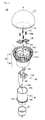
Fig. 1 is a perspective view showing an embodiment of a lighting device.Fig. 2 is an exploded perspective view of the lighting device shown inFig. 1 ,Fig. 3 is a cross sectional view of the lighting device shown inFig. 1 .Fig. 4 is a perspective view of a light emitting module shown inFig. 1 . - Referring to
Figs. 1 to 4 , alighting device 100 may include acover 110, alight emitting module 130, aheat sink 140, apower controller 150 and aninner case 160. - The
cover 110 surrounds and protects thelight emitting module 130 from external impacts. Thecover 110 also distributes light generated by thelight emitting module 130 to the front or rear (top or bottom) of thelighting device 100. - The
heat sink 140 radiates heat to the outside generated from thelight emitting module 130 due to the drive of thelighting device 100. Theheat sink 140 improves heat radiation efficiency through as much surface contact with thelight emitting module 130 as possible. Here, theheat sink 140 may be coupled to thelight emitting module 130 by using an adhesive. Additionally, it is recommended that they should be coupled to each other by using a fastening means 120b, for example, a screw. - The
inner case 160 receives thepower controller 150 therein, and then is received by theheat sink 140. - Hereafter, the
lighting device 100 according to the embodiment will be described in detailed focusing on its constituents. - The
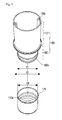
cover 110 has a bulb shape having an opening 'G1'. The inner surface of thecover 110 may be coated with an opalesque pigment. The pigment may include a diffusing material such that light passing through thecover 110 can be diffused throughout the inner surface of thecover 110. - The
cover 110 may be formed of glass. However, the glass is vulnerable to weight or external impact. Therefore, plastic, polypropylene (PP) and polyethylene (PE) and the like can be used as the material of thecover 110. Here, polycarbonate (PC), etc., having excellent light resistance, excellent thermal resistance and excellent impact strength property can be also used as the material of thecover 110. - The
light emitting module 130 may include asubstrate 131 and alight source unit 133 disposed on thesubstrate 130. - The
substrate 131 has a quadrangular shape and there is no limit to the shape of thesubstrate 130. However, as shown in the embodiment, when thesubstrate 131 has a quadrangular shape, thesubstrate 130 has ahole 131a in its central portion and a via-hole 131b in its corner portion. When a plurality of thesubstrates 131 are disposed on a specific surface like one surface of theheat sink 140, the viahole 131b can function as a path for wiring or a connector for electrically connecting the adjacent substrates. - The
substrate 131 may be formed by printing a circuit pattern on an insulator and may include, for example, a common printed circuit board (PCB), a metal core PCB, a flexible PCB and a ceramic PCB and the like. Here, thesubstrate 131 may be a chips on board (COB) allowing an unpackaged LED chip to be directly bonded thereon. The COB type substrate includes a ceramic material to obtain insulation and thermal resistance against heat generated by driving thelighting device 100. - The
substrate 131 may be also formed of a material capable of efficiently reflecting light, or the surface of thesubstrate 131 may have color capable of efficiently reflecting light, for example, white and silver and the like. - A plurality of the
light source unit 133 may be disposed on thesubstrate 131. Thelight source unit 133 may include a light emitting device 133-1 and a lens 133-3. - A plurality of the light emitting device 133-1 may be disposed on one side of the
substrate 131. The light emitting device 133-1 may be a light emitting diode chip emitting blue, red or green light or may be a light emitting diode chip emitting UV. - Also, the light emitting diode of the light emitting device 133-1 may have a lateral type or a vertical type. The light emitting diode may emit blue, red or green light.
- The lens 133-3 is disposed on the
substrate 131 in such a manner as to cover the light emitting device 133-1. The lens 133-3 is able to adjust the orientation angle or direction of light emitted from the light emitting device 133-1. - The lens 133-3 has a hemispherical shape. The inside of the lens 133-3 may be entirely filled with a light transmitting resin like a silicon resin or epoxy resin without an empty space. The light transmitting resin may entirely or partially include distributed fluorescent material.
- Here, when the light emitting device 133-1 is a blue light emitting diode, the fluorescent material included in the light transmitting resin of the lens 133-3 may include at least any one selected from a group consisting of a garnet based material (YAG, TAG), a silicate based material, a nitride based material and an oxynitride based material.
- Though natural light (white light) can be created by allowing the light transmitting resin to include only yellow fluorescent material, the light transmitting resin may further include a green fluorescent material or a red fluorescent material in order to improve a color rendering index and to reduce a color temperature.
- When the light transmitting resin of the lens 133-3 is mixed with many kinds of fluorescent materials, an addition ratio of the color of the fluorescent material may be formed such that the green fluorescent material is more used than the red fluorescent material, and the yellow fluorescent material is more used than the green fluorescent material.
- The garnet based material, the silicate based material and the oxynitride based material may be used as the yellow fluorescent material. The silicate based material and the oxynitride based material may be used as the green fluorescent material. The nitride based material may be used as the red fluorescent material.
- The lens 133-3 may be formed not only by mixing the fluorescent material with the light transmitting resin, but also by stacking layers including the red, green and yellow fluorescent materials.
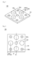
-
Fig. 5 is a view for describing thelight emitting module 130 shown inFig. 1 ; - Referring to
Figs. 1 and5 , thesubstrate 131 may include thehole 131a and the via-hole 131b. Thehole 131a may be placed at the center of thesubstrate 131 and the via-hole 131b may be placed in each corner of thesubstrate 131. Thehole 131a may function as either a standard for the arrangement of thelight source units 133 or a hole through which the fastening means 120b, for example, a screw, is passed when thesubstrate 131 is coupled to theheat sink 140. When a plurality of the substrates are disposed on theheat sink 140, the via-hole 131b the viahole 131b can function as a path for wiring or a connector for electrically connecting the adjacent substrates. - A plurality of the
light source units 133 may be disposed up, down, right and left with respect to thehole 131 a formed at the center of thesubstrate 131. The plurality of thelight source units 133 may be disposed symmetrically with each other with respect to thehole 131a. Here, though thelight source units 133 may be disposed on thesubstrate 131 in various forms, it is recommended that thelight source units 133 should be disposed symmetrically with respect to thehole 131a for the purpose of improvement of the uniformity characteristics of light emitted from thelight source units 133. - A distance "d1" from the center of the
light source unit 133 to the center of thehole 131a formed at the center of thesubstrate 131 is greater than a distance "d2" from the center of thelight source unit 133 to the edge of thesubstrate 131. This intends to improve the uniformity characteristics of the light emitted from thelight emitting module 130. If "d1" is less than "d2", the uniformity characteristics of the light is substantially deteriorated because the light emitted from thelight emitting module 130 is focused entirely on the central portion of thelight emitting module 130. -
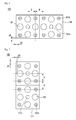
Figs. 6 and 7 are views for describing an arrangement of a plurality of the light emitting modules shown inFig. 1 . - Referring to
Figs. 6 and 7 , substrates of two light emitting modules are disposed adjacent to each other. A distance "D" from the center of the light source unit of a first light emitting module to the center of a hole of a first light emitting module (that is, a light emitting module placed to the left ofFig. 6 and a light emitting module placed on the upper side ofFig. 7 ) out of the two light emitting modules is the same as a distance "D" from the center of the light source unit of the first light emitting module to the center of the light source unit of a second light emitting module (that is, a light emitting module placed to the right ofFig. 6 and a light emitting module placed on the lower side ofFig. 7 ). Accordingly, light generated from two adjacentlight emitting modules 130 is able to maintain the uniformity characteristics as it is of light generated from onelight emitting module 130. - Regarding the plurality of the
light source units 133, distances "d3" from the end of thesubstrate 131 to the ends of the plurality of thelight source units 133 may be the same as each other. -
Fig. 8 is a view for describing another embodiment of the light emitting module shown inFig. 4 . - Referring to
Fig. 8 , like thelight emitting module 130 shown inFig. 5 , a light emitting module 130' includes thesubstrate 131 and thelight source unit 133. The descriptions of thesubstrate 131 and thelight source unit 133 which are shown inFig. 8 can be replaced with the foregoing descriptions. - The
light source unit 133 and the via-hole 131b of the light emitting module 130' shown inFig. 8 are disposed differently from thelight source unit 133 and the via-hole 131b of thelight emitting module 130 shown inFig. 5 . - The via-
holes 131b of the light emitting module 130' shown inFig. 8 are disposed up, down, right and left with respect to thehole 131a formed at the center of thesubstrate 131. Thelight source unit 133 is disposed in each corner of thesubstrate 131. - The
heat sink 140 includes a receivingrecess 140a into which thepower controller 150 and theinner case 160 are inserted. - The
heat sink 140 may include one surface "p" on which thelight emitting module 130 is disposed. The one surface "p" may be, as shown in the drawings, flat or may be curved to have a predetermined curvature. The one surface "p" may be also, as shown in the drawings, circular or may be polygonal or elliptical. - The one surface "p" may include a seating recess 141-1 in which at least one light emitting
module 130 is seated. The one surface "p" may also include afirst recess 141a, asecond recess 141b and athird recess 141c. - A first fastening means 120a like a
first screw 120a is inserted into thefirst hole 141a, and then thefirst screw 120a is inserted into afastening hole 160a formed in the inner surface of theinner case 160, so that theheat sink 140 is coupled to theinner case 160. - A second fastening means 120b like a
second screw 120b which has passed through thehole 131a formed at the center of thelight emitting module 130 is inserted into thesecond hole 141b, so that theheat sink 140 is coupled to thelight emitting module 130. Accordingly, heat generated from thelight emitting module 130 is effectively transferred to theheat sink 140. As a result, heat radiating characteristic can be improved. - An
electrode pin 150a of thepower controller 150 passes through thethird hole 141c. Theelectrode pin 150a which has passed through thethird hole 141c may be inserted into toe via-hole 131b of thelight emitting module 130. - The
heat sink 140 may include an upper portion 141 and alower portion 143. The upper portion 141 may have a cylindrical shape. The cylindrical upper portion 141 may have the one surface "p" on which thelight emitting module 130 is disposed. Thelower portion 143 may have a cylindrical shape. The cylindricallower portion 143 extends from the cylindrical upper portion 141. The diameter of the cylindricallower portion 143 decreases downward along a central axis "A" which penetrates the center of the one surface "p". - Either the area or the height of the one surface "p" of the cylindrical upper portion 141 may be changed according to the total volume of the
light emitting module 130 or the entire length of thepower controller 150. - Fins 141-2 may be disposed on the lateral surface of the
heat sink 140. Specifically, a plurality of the fins 141-2 may be disposed on the lateral surface of the cylindrical upper portion 141 in the longitudinal direction of the cylindrical upper portion 141. The plurality of the fins 141-2 may be radially disposed along the surface of the cylindrical upper portion 141. The plurality of the fins 141-2 increase the surface area of the cylindrical upper portion 141 to improve the heat radiation efficiency. Here, although the plurality of the fins 141-2 are formed only on the cylindrical upper portion 141 in the drawings, the plurality of the fins 141-2 may be also formed on the surface of the cylindricallower portion 143. For example, the plurality of the fins 141-2 may be formed extending from the surface of the cylindrical upper portion 141 to the surface of the cylindricallower portion 143. - The
heat sink 140 is formed of a metallic material or a resin material which has excellent heat radiation efficiency. There is no limit to the material of theheat sink 140. For example, the material of theheat sink 140 can include at least one of Al, Ni, Cu, Ag and Sn. - Though not shown in the drawings, a heat radiating plate (not shown) may be disposed between the light emitting
module 130 and theheat sink 140. The heat radiating plate (not shown) may be formed of a material having a high thermal conductivity such as a thermal conduction silicon pad or a thermal conduction tape and the like, and is able to effectively transfer heat generated by thelight emitting module 130 to theheat sink 140. - The
power controller 150 includes asupport plate 151 and a plurality ofparts 153 mounted on thesupport plate 151. The plurality of theparts 153 includes, for example, a DC converter converting AC power supplied by an external power supply into DC power, a driving chip controlling the driving of thelight emitting module 130, and an electrostatic discharge (ESD) protective device for protecting thelight emitting module 130, and the like. However, there is no limit to the parts. - The
power controller 150 may include theelectrode pin 150a which projects outwardly from thesupport plate 151 or is connected to thesupport plate 151. - The
electrode pin 150a may pass through thethird hole 141c formed in the cylindrical upper portion 141 of theheat sink 140, and may be inserted into the via-hole 131b of thelight emitting module 130. Theelectrode pin 150a supplies electric power to thelight emitting module 130 from thepower controller 150. - The
inner case 160 may include aninsertion portion 161 which is inserted into the receivingrecess 140a of theheat sink 140, and aconnector 163 which is electrically connected to an external power supply. - The
inner case 160 may be formed of a material having excellent insulation and durability, for example, a resin material. - The
insertion portion 161 has a cylindrical shape with an empty interior. Theinsertion portion 161 is inserted into the receivingrecess 140a of theheat sink 140 and prevents an electrical short-circuit between thepower controller 150 and theheat sink 140. Therefore, a withstand voltage of thelighting device 100 can be improved. - The
insertion portion 161 may include thefastening hole 160a. Thefastening hole 160a may be formed in the inner surface of theinsertion portion 161. Thefirst screw 120a which has passed through thefirst recess 141a of theheat sink 140 is inserted and fixed to thefastening hole 160a. - The
insertion portion 161 may include aguide 161 a. Theguide 161 a may be formed to project from the outer circumferential surface of theinsertion portion 161. When theinsertion portion 161 is inserted into the receivingrecess 140a of theheat sink 140, theguide 161a supports the side ends of the receivingrecess 140a of theheat sink 140. - The
connector 163 may be formed extending from theinsertion portion 161. Theconnector 163 may be coupled to asocket 170. - The
socket 170 is coupled to theconnector 163 of theinner case 160 and is electrically connected to an external power supply. - The
power controller 150 may be disposed in the receivingrecess 140a of theheat sink 140. - The
support plate 151 of thepower controller 150 may be disposed perpendicularly with respect to one side of thesubstrate 131 such that air flows smoothly in theinner case 160. Accordingly, as compared with a case where thesupport plate 151 is disposed horizontally with respect to one side of thesubstrate 131, air flows up and down in theinner case 160 due to convection current, thereby improving the heat radiation efficiency of thelighting device 100. - Meanwhile, the
support plate 151 may be disposed in theinner case 160 perpendicularly to the longitudinal direction of theinner case 160. There is no limit to how thesupport plate 151 is disposed. - The
power controller 150 may be electrically connected to thesocket 170 through afirst wiring 150b and may be electrically connected to thelight emitting module 130 through theelectrode pin 150a. Specifically, thefirst wiring 150b is connected to thesocket 170, and then can be supplied an electric power from an external power supply. Also, theelectrode pin 150a passes through thethird recess 141c of theheat sink 140 and is able to electrically connect thepower controller 150 with thelight emitting module 130. -
Fig. 9 is a view for describing the coupling of an inner case and the socket which are shown inFig. 2 . - Referring to
Fig. 9 , theinner case 160 can be coupled to thesocket 170 by the rotation of thesocket 170. For example, when the outer surface of theconnector 163 of theinner case 160 includes ascrew thread 163a and the inner surface of thesocket 170 includes ascrew groove 170a corresponding to thescrew thread 163a, theinner case 160 can be coupled to thesocket 170 by the coupling of the screw thread and the screw groove. Here, the outer surface of theconnector 163 of theinner case 160 may include the screw groove and the inner surface of thesocket 170 may include the screw thread corresponding to the screw groove. - The diameter "d1" of the
connector 163 of theinner case 160 is less than the diameter "d2" of theinsertion portion 161 of theinner case 160. Also, the diameter "d3" of thesocket 170 is less than the diameter "d2" of theinsertion portion 161 of theinner case 160. This intends to allow thelighting device 100 to have a shape capable of substituting for a conventional lighting device. - While the
inner case 160 includes theinsertion portion 161 and theconnector 163 having a diameter less than that of theinsertion portion 161, theinsertion portion 161 and theconnector 163 are allowed to have the same diameter as one body. In this case, a screw thread or a screw groove is formed on the outer surface of theconnector 163, and then theconnector 163 is coupled to thesocket 170. Such a structure improves assemblability of the lighting device and makes it easier to repair structures like thepower controller 150 disposed in theinner case 160. -
Figs. 10a to 10h are views for describing an assembly process of the lighting device shown inFig. 2 . - Referring to
Fig. 10a , thepower controller 150 is inserted into theinsertion portion 161 of theinner case 160. Here, though not shown, a guider groove (not shown) may be formed in the inner surface of theinner surface 160 such that thesupport plate 151 1 of thepower controller 150 is coupled to the inner surface of theinner case 160 in a sliding manner. The guider groove (not shown) may be formed in the longitudinal direction of theinner case 160. - Next, referring to
Fig. 10b , aholder 155 is located at the end of theinsertion portion 161 of theinner case 160 and seals theinner case 160 such that theelectrode pin 150a of thepower controller 150 disposed in theinsertion portion 161 of theinner case 160 is securely fixed and electrically coupled to thelight emitting module 130. Here, theholder 155 includes aprotrusion portion 155a having a through-hole allowing theelectrode pin 150a to pass through the through-hole. Theholder 155 also includes anauxiliary hole 155b allowing thefirst screw 120a fastening the heat sink140 to theinner case 160 to pass through theauxiliary hole 155b. Since theholder 155 functions as a means for securely fixing and supporting theelectrode pin 150a, theholder 155 may not be used in some cases. - Next, referring to
Fig. 10b , an assembly of theinner case 160 and thepower controller 150 is coupled to theheat sink 140. In this case, theinsertion portion 161 of theinner case 160 is inserted into the receivingrecess 140a of theheat sink 140 shown inFig. 3 . Theinner case 160 and theheat sink 140 are fixed by thefirst screw 120a. Here, theelectrode pin 150a of thepower controller 150 passes through thethird hole 141c of theheat sink 140 and projects. - Referring to
Fig. 10d , thesocket 170 is coupled to theconnector 163 of theinner case 160. Through a wiring connection, thesocket 170 is electrically connected to thepower controller 150 disposed in theinner case 160. - Referring to
Fig. 10e , athermal grease 134 is applied on the bottom surface of thesubstrate 131 of the provided light emittingmodule 130. Thelight emitting module 130 includes a plurality of thelight source units 133. Thelight source units 133 are disposed symmetrically with each other with respect to thehole 131a formed at the center of thesubstrate 131. Specifically, thelight source units 133 are disposed on thesubstrate 131 symmetrically up, down, right and left with respect to thehole 131a formed at the center of thesubstrate 131. Though thelight source units 133 may be disposed on thesubstrate 131 in various forms, it is recommended that thelight source units 133 should be disposed symmetrically with respect to thehole 131a for the purpose of improvement of the uniformity characteristics of light emitted from thelight source units 133. - Referring to
Fig. 10f , thelight emitting module 130 and an assembly including theinner case 160, thepower controller 150 and theheat sink 140 are coupled to each other by using thesecond screw 120b. Here, thesecond screw 120b fixes the light emitting module to the assembly by passing through thehole 131 formed at the central portion of thelight emitting module 130 and thesecond hole 141b of theheat sink 140. - Referring to
Fig. 10g , aconnector 135 is connected to each via-hole 131b of two light emittingmodules 130 such that the twolight emitting modules 130 are electrically connected to each other. Here, theelectrode pin 150a of thepower controller 150 is soldered in such a manner as to be electrically connected to thesubstrate 131 of thelight emitting module 130. - Referring to
Fig. 10h , thecover 110 is silicon-bonded and coupled to the heat sink in such a manner as to cover thelight emitting module 130. - Since the
lighting device 100 has a structure capable of substituting for a conventional incandescent bulb, it is possible to use equipments for the conventional incandescent bulb without the use of a mechanical connection structure for a new lighting device or without the improvement of assembly. -
Fig. 11 is a perspective view of a lighting device according to further another embodiment.Fig. 12 is an exploded perspective view of the lighting device shown inFig. 11 .Fig. 13 is a cross sectional view of the lighting device shown inFig. 11 . - Referring to
Figs. 11 to 13 , alighting device 200 according to another embodiment may include acover 210, alight emitting module 230, aheat sink 240, apower controller 250, aninner case 260 and anouter case 270. - The
cover 210 surrounds and protects thelight emitting module 230 from external impacts. Thecover 210 also distributes light generated by thelight emitting module 230 to the front or rear (top or bottom) of thelighting device 200. - The
heat sink 240 radiates heat to the outside generated from thelight emitting module 230 due to the drive of thelighting device 200. Theheat sink 240 improves heat radiation efficiency through as much surface contact with thelight emitting module 230 as possible. Theouter case 270 receives theheat sink 240, thepower controller 250 and theinner case 260 and the like. Theouter case 270 and thecover 210 determine the external appearance of thelighting device 200. Here, theouter case 270 may not be used. - Hereafter, the
lighting device 200 according to the embodiment will be described in detail focusing on its constituents. - The
cover 210 has a bulb shape having an opening "G1". The inner surface of thecover 210 may be coated with an opalesque pigment. The pigment may include a diffusing material such that light which is passing through thecover 210 can be diffused throughout the inner surface of thecover 210. - The
cover 210 may be formed of glass. However, the glass is vulnerable to weight or external impact. Therefore, plastic, polypropylene (PP) and polyethylene (PE) and the like can be used as the material of thecover 210. Here, polycarbonate (PC), etc., having excellent light resistance, excellent thermal resistance and excellent impact strength property can be also used as the material of thecover 210. - The
light emitting module 230 may include asubstrate 231 and a plurality oflight source units 233 mounted on thesubstrate 231. - The
substrate 231 and thelight source unit 233 may be the same as thesubstrate 131 and thelight source unit 133 shown inFig. 4 . The detailed description thereof is replaced with the foregoing description. - A plurality of the
light emitting modules 230 may be disposed on one flat surface of anupper portion 241 of theheat sink 240. Specifically, threelight emitting modules 230 may be disposed in two rows. That is, twolight emitting modules 230 may be disposed in a first row and onelight emitting module 230 may be disposed in a second row. The threelight emitting modules 230 may be disposed entirely in the form of a triangle. - The plurality of the
light emitting modules 230 may be disposed apart from each other at an interval on one surface of theheat sink 240, and preferably may be disposed adjacent to each other. Although thelight emitting modules 230 are disposed adjacent to each other, thelight source units 233 of thelight emitting modules 230 may be uniformly disposed apart from each other at a regular interval. Further, thelight source units 233 disposed in two adjacentlight emitting modules 230 may be uniformly disposed apart from each other at a regular interval. As a result, substantially, light emitted from the entirelight emitting modules 230 is able to have uniformity characteristics as it is of light generated from onelight emitting module 230. - Color temperatures of light emitted from the plurality of the
light emitting modules 230 may be different from each other. This can be implemented by varying the kind of fluorescent material included in thelight source unit 233 of thelight emitting module 230. When the color temperatures of light emitted from the plurality of thelight emitting modules 230 are different from each other, it is possible to create emotional lighting. - The number and the disposition of the
light emitting module 230 are not limited to the example shown in the drawings and may be changed according to the size of theheat sink 240, the light amount of thelight emitting module 230 and the number of thelight source units 233 included in thelight emitting module 230. For example, while the embodiment shows the plurality of thelight emitting modules 230 are disposed in theheat sink 240 in two rows, thelight emitting modules 230 may be disposed in theheat sink 240 in two or more rows as the size of theheat sink 240 increases. Besides, the number of thelight emitting modules 230 may also increase. - The
light emitting module 230 shown inFigs. 11 to 13 can be used as thelight emitting module 130 shown inFigs. 1 to 3 . - The
heat sink 240 includes a receivingrecess 240a into which thepower controller 250 and theinner case 260 are inserted. - The
heat sink 240 may include one surface "p" on which the plurality of thelight emitting modules 230 are disposed. The one surface "p" may be, as shown in the drawings, flat or may be curved to have a predetermined curvature. The one surface "p" may be also, as shown in the drawings, circular or may be polygonal or elliptical. - The one surface "p" may include a
seating recess 241b in which thelight emitting module 230 is seated. The one surface "p" may also include ahole 241a through which afirst wiring 250a passes. Thefirst wiring 250a electrically connects the plurality of thelight emitting modules 230 with thepower controller 250. Thehole 241a may be disposed at the center of the one surface "p". - The
heat sink 240 may include anupper portion 241 and alower portion 243. Theupper portion 241 may have a cylindrical shape. The cylindricalupper portion 241 may have the one surface "p" on which thelight emitting module 230 is disposed. The diameter of the cylindricalupper portion 241 increases the farther it is from the one surface "p". Therefore, the cylindricalupper portion 241 has the one surface "p" and a surface inclined toward the cylindricallower portion 243 at an acute angle with respect to the one surface "p". The inclined surface of the cylindricalupper portion 241 facilitates a rear light distribution of thelighting device 200 according to the embodiment. - The
lower portion 243 may have a cylindrical shape and extends from the cylindricalupper portion 241. The diameter of the cylindricallower portion 243 decreases the closer it gets to the bottom thereof. - The area of the one surface "p" of the cylindrical
upper portion 241 or the height of the cylindricalupper portion 241 may be changed according to the total volume of thelight emitting module 230 or the entire length of thepower controller 250. - A plurality of
grooves 243a may be formed on the surface of the cylindricallower portion 243 in the longitudinal direction of the cylindricallower portion 243. The plurality of thegrooves 243a may be radially disposed along the surface of the cylindricallower portion 243. The grooves of the cylindricallower portion 243 increase the surface area of theheat sink 240 to improve the heat radiation efficiency. - Although the plurality of the
grooves 243a are formed only on the cylindricallower portion 243 in the drawings, the plurality of the grooves may be also disposed on the surface of the cylindricalupper portion 241. For example, the plurality of thegrooves 243a may be formed extending from the surface of the cylindricallower portion 243 to the surface of the cylindricalupper portion 241. - The
heat sink 240 is formed of a metallic material or a resin material which has excellent heat radiation efficiency. There is no limit to the material of theheat sink 240. For example, the material of theheat sink 140 can include at least one of A1, Ni, Cu, Ag and Sn. - Though not shown in the drawings, a heat radiating plate (not shown) may be disposed between the light emitting
module 230 and theheat sink 240. The heat radiating plate (not shown) may be formed of a material having a high thermal conductivity such as a thermal conduction silicon pad or a thermal conduction tape and the like, and is able to effectively transfer heat generated by thelight emitting module 230 to theheat sink 240. - The
power controller 250 includes asupport plate 251 and a plurality ofparts 253 mounted on thesupport plate 251. The plurality of theparts 253 includes, for example, a DC converter converting AC power supplied by an external power supply into DC power, a driving chip controlling the driving of thelight emitting module 230, and an electrostatic discharge (ESD) protective device for protecting thelight emitting module 230, and the like. However, there is no limit to the parts. - The
inner case 260 may include aninsertion portion 261 which is inserted into the receivingrecess 240a of theheat sink 240, and aconnection terminal 263 which is electrically connected to an external power supply. - The
inner case 260 may be formed of a material having excellent insulation and durability, for example, a resin material. - The
insertion portion 261 has a cylindrical shape with an empty interior. Theinsertion portion 261 is inserted into the receivingrecess 240a of theheat sink 240 and prevents an electrical short-circuit between thepower controller 250 and theheat sink 240. Therefore, a withstand voltage of thelighting device 200 can be improved. - The
connection terminal 263 may be connected, for example, to an external power supply in the form of a socket. That is, theconnection terminal 263 includes afirst electrode 263a at the apex thereof, asecond electrode 263b on the lateral surface thereof, and an insulatingmember 263c between thefirst electrode 263a and thesecond electrode 263b. Electric power is supplied to thefirst electrode 263a and thesecond electrode 263b from an external power supply. Here, since the shape of theconnection terminal 263 is variously changed according to the design of thelighting device 200, there is no limit to the shape of theconnection terminal 263. - The
power controller 250 may be disposed in the receivingrecess 240a of theheat sink 240. - The
support plate 251 of thepower controller 250 may be disposed perpendicularly with respect to one side of thesubstrate 231 such that air flows smoothly in theinner case 160. Accordingly, as compared with a case where thesupport plate 251 is disposed horizontally with respect to one side of thesubstrate 231, air flows up and down in theinner case 260 due to convection current, thereby improving the heat radiation efficiency of thelighting device 200. - Meanwhile, the
support plate 251 may be disposed in theinner case 260 perpendicularly to the longitudinal direction of theinner case 260. There is no limit to how thesupport plate 251 is disposed. - The
power controller 250 may be electrically connected to thelight emitting module 230 through thefirst wiring 250a and may be electrically connected to theconnection terminal 263 of theinner case 260 through asecond wiring 260a. Specifically, thesecond wiring 260a is connected to thefirst electrode 263a and thesecond electrode 263b of theconnection terminal 263, and then can be supplied an electric power from an external power supply. Also, thefirst wiring 250a passes through thehole 241a of theheat sink 140 and is able to electrically connect thepower controller 250 with thelight emitting module 230. - The
outer case 270 surrounds theheat sink 240. Specifically, theouter case 270 surrounds a portion of the lateral surface of theheat sink 240. - The
outer case 270 may be disposed separately from the lateral surface of theheat sink 240 at a predetermined interval. This intends to prevent heat from theheat sink 240 from being directly transferred to theouter case 270. - The
outer case 270 allows a user to easily handle thelighting device 200 and prevents an electric shock and a burn accident due to theheat sink 240. - The
outer case 270 may include aring structure 271 coupled to theinner case 260, a cone-shapedbody 273 having a central opening, and aconnection portion 275 that physically connects thering structure 271 with thebody 273. - The
body 273 has a cone shape. Thebody 273 has a shape corresponding to that of the cylindricallower portion 243 of theheat radiating body 240. Thebody 273 may be disposed separately from the cylindricallower portion 243 of theheat radiating body 240 at a predetermined interval. - The
connection portion 275 may be comprised of a plurality of ribs. An opening "G2" is formed among the plurality of the ribs. The heat from theheat sink 240 may be radiated to the outside through the opening "G2". - The
outer case 270 may be formed of a material having excellent insulation and durability, for example, a resin material. - Since the
lighting device 200 has a structure capable of substituting for a conventional incandescent bulb, it is possible to use equipments for the conventional incandescent bulb without the use of a mechanical connection structure for a new lighting device or without the improvement of assembly. -
Fig. 14 is a view for describing the coupling of a heat sink and a light emitting module of the lighting device shown inFig. 12 . - Referring to
Fig. 14 , theheat sink 240 includes aseating portion 241b which is formed on the one surface "p" of the cylindricalupper portion 241 and has a predetermined depth. The depth of theseating portion 241b may be the same as the thickness of thesubstrate 231. The outer circumference of theseating portion 241b may include at least one recess (not shown). - The
seating portion 241b may have any shape corresponding to the shape of thesubstrate 231. An outer recess (not shown) formed in the outer circumference of theseating portion 241b may be disposed inward or outward with respect to the outer circumference of theseating portion 241b. - Specifically, when the outer recess (not shown) of the
seating portion 241b of theheat sink 240 is formed outwardly with respect to the outer circumference of theseating portion 241b, the outer circumferential surface of thesubstrate 231 may include a protrusion portion (not shown) which is inserted and fixed into the outer recess (not shown) of theseating portion 241b of theheat sink 240. - When the outer recess (not shown) of the
seating portion 241b of theheat sink 240 is formed inwardly with respect to the outer circumference of theseating portion 241b, the outer circumferential surface of thesubstrate 231 may include a recess corresponding to theseating portion 241b of theheat sink 240. - The coupling structure mentioned above prevents the
substrate 231 from rotating or separating. Therefore, alignment characteristic between theheat sink 240 and thelight emitting module 230 can be improved. - Any reference in this specification to "one embodiment," "an embodiment," "example embodiment," etc., means that a particular feature, structure, or characteristic described in connection with the embodiment is included in at least one embodiment of the invention. The appearances of such phrases in various places in the specification are not necessarily all referring to the same embodiment. Further, when a particular feature, structure, or characteristic is described in connection with any embodiment, it is submitted that it is within the purview of one skilled in the art to affect such feature, structure, or characteristic in connection with other ones of the embodiments.
- Although embodiments have been described with reference to a number of illustrative embodiments thereof, it should be understood that numerous other modifications and embodiments can be devised by those skilled in the art that will fall within the spirit and scope of the principles of this disclosure. More particularly, various variations and modifications are possible in the component parts and/or arrangements of the subject combination arrangement within the scope of the disclosure, the drawings and the appended claims. In addition to variations and modifications in the component parts and/or arrangements, alternative uses will also be apparent to those skilled in the art.
Claims (15)
- A lighting device comprising:a heat sink which includes one surface and a receiving recess;a light emitting module which is disposed on the one surface of the heat sink and includes a substrate and a plurality of light sources disposed on the substrate, wherein the substrate includes a hole and a plurality of via-holes;a power controller which includes an electrode pin electrically connected to the light emitting module through the via-hole; andan insulating inner case which receives the power controller therein and is disposed in the receiving recess of the heat sink,wherein the light sources include an lighting emitting device.
- The lighting device of claim 1, wherein a lens covering the light emitting device and including a resin and a fluorescent material, and wherein the fluorescent material includes at least two of a yellow fluorescent material, a green fluorescent material and/or a red fluorescent material.
- The lighting device of claim 1 or 2, wherein a distance from the center of the light source to the center of the hole is greater than a distance from the center of the light source to the edge of the substrate.
- The lighting device of any one claim of claims 1 to 3, wherein the hole of the substrate is disposed at the center of the substrate, and wherein the plurality of the light sources are disposed symmetrically with each other with respect to the hole of the substrate.
- The lighting device of any one claim of claims 1 to 4, wherein the light emitting module comprises a first light emitting module and a second light emitting module, wherein the substrate of the first light emitting module and the substrate of the second light emitting module are disposed adjacent to each other, and wherein a distance from the center of the light source of the first light emitting module to the center of a hole of the first light emitting module is the same as a distance from the center of the light source of the first light emitting module adjacent to the second light emitting module to the center of the light source of the second light emitting module adjacent to the first light emitting module.
- The lighting device of any one claim of claims 1 to 5, further comprising a cover which is disposed on the light source, protects the light source and has a material diffusing light generated from the light source.
- The lighting device of any one claim of claims 1 to 6, wherein the light emitting module comprises a first light emitting module and a second light emitting module, and comprising a connector which electrically connects the first light emitting module with the second light emitting module.
- The lighting device of any one claim of claims 1 to 7, wherein the light emitting module comprises a first light emitting module and a second light emitting module, wherein the one surface of the heat sink comprises a first seating recess in which the first light emitting module is disposed and a second seating recess in which the second light emitting module is disposed, and wherein the first seating recess and the second seating recess are partially connected with each other.
- The lighting device of any one claim of claims 1 to 8, wherein the light emitting module comprises a first light emitting module and a second light emitting module, wherein the first and the second light emitting modules emit white light, and wherein the white light of the first light emitting module has a color temperature different from that of the white light of the second light emitting module.
- The lighting device of any one claim of claims 1 to 3, wherein at least three light emitting modules are provided and wherein the at least three light emitting modules are disposed on the one surface of the heat sink in the shape of "T".
- The lighting device of any one claim of claims 1 to 10, wherein the heat sink comprises an upper portion and a lower portion, and wherein the upper portion comprises both a first area having the one surface and a second area having a surface inclined with respect to the one surface.
- The lighting device of any one claim of claims 1 to 11, further comprising a holder which is coupled to the inner case in order to seal the power controller and includes an insulating portion for insulating the electrode pin from the heat sink.
- The lighting device of any one claim of claims 1 to 12, wherein the inner case comprises a fastening hole, and wherein the heat sink comprises a hole which corresponds to the fastening hole and passes through the one surface, and comprising a fastening means which fixes the heat sink to the inner case by passing through the hole of the heat sink and being coupled to the fastening hole of the inner case.
- The lighting device of any one claim of claims 1 to 13, comprising a socket which is coupled to the inner case and electrically connected to the power controller, wherein the socket includes a screw groove and wherein the inner case includes a screw thread corresponding to the screw groove.
- The lighting device of any one claim of claims 1 to 14, wherein the heat sink comprises a lateral surface, further comprising an outer case surrounding the lateral surface of the heat sink, and wherein the outer case is disposed separately from the lateral surface of the heat sink at a predetermined interval and surrounds at least a portion of the lateral surface of the heat sink.
Priority Applications (1)
| Application Number | Priority Date | Filing Date | Title |
|---|---|---|---|
| EP14195568.2A EP2848857B1 (en) | 2010-11-08 | 2011-10-25 | Lighting device |
Applications Claiming Priority (3)
| Application Number | Priority Date | Filing Date | Title |
|---|---|---|---|
| KR1020100110464A KR101080699B1 (en) | 2010-11-08 | 2010-11-08 | Light module and lighting device including the same |
| KR1020100113542A KR101063925B1 (en) | 2010-11-15 | 2010-11-15 | Lighting device |
| KR1020100122745A KR101742674B1 (en) | 2010-12-03 | 2010-12-03 | Lighting device |
Related Child Applications (2)
| Application Number | Title | Priority Date | Filing Date |
|---|---|---|---|
| EP14195568.2A Division EP2848857B1 (en) | 2010-11-08 | 2011-10-25 | Lighting device |
| EP14195568.2A Division-Into EP2848857B1 (en) | 2010-11-08 | 2011-10-25 | Lighting device |
Publications (3)
| Publication Number | Publication Date |
|---|---|
| EP2450613A2 true EP2450613A2 (en) | 2012-05-09 |
| EP2450613A3 EP2450613A3 (en) | 2012-11-28 |
| EP2450613B1 EP2450613B1 (en) | 2015-01-28 |
Family
ID=45033729
Family Applications (2)
| Application Number | Title | Priority Date | Filing Date |
|---|---|---|---|
| EP11186424.5A Active EP2450613B1 (en) | 2010-11-08 | 2011-10-25 | Lighting device |
| EP14195568.2A Active EP2848857B1 (en) | 2010-11-08 | 2011-10-25 | Lighting device |
Family Applications After (1)
| Application Number | Title | Priority Date | Filing Date |
|---|---|---|---|
| EP14195568.2A Active EP2848857B1 (en) | 2010-11-08 | 2011-10-25 | Lighting device |
Country Status (3)
| Country | Link |
|---|---|
| US (2) | US8757841B2 (en) |
| EP (2) | EP2450613B1 (en) |
| CN (2) | CN102466160B (en) |
Cited By (1)
| Publication number | Priority date | Publication date | Assignee | Title |
|---|---|---|---|---|
| DE102011084795A1 (en) * | 2011-10-19 | 2013-04-25 | Osram Gmbh | Semiconductor lighting device with galvanically non-isolated driver |
Families Citing this family (34)
| Publication number | Priority date | Publication date | Assignee | Title |
|---|---|---|---|---|
| CN103547853B (en) * | 2011-05-20 | 2016-05-04 | 松下知识产权经营株式会社 | Lamp |
| US20140119034A1 (en) * | 2011-06-14 | 2014-05-01 | Ming-Yun Chen | Inductive illumination apparatus |
| KR101326518B1 (en) | 2011-09-02 | 2013-11-07 | 엘지이노텍 주식회사 | Lighting device |
| US9212801B2 (en) * | 2011-11-23 | 2015-12-15 | Huizhou Light Engine Ltd. | Electrical connections for a light-emitting diode lamp |
| KR20130080259A (en) * | 2012-01-04 | 2013-07-12 | 삼성전자주식회사 | Light emitting device |
| KR102017538B1 (en) | 2012-01-31 | 2019-10-21 | 엘지이노텍 주식회사 | Lighting device |
| US9234647B2 (en) | 2012-05-03 | 2016-01-12 | Abl Ip Holding Llc | Light engine |
| US8680755B2 (en) * | 2012-05-07 | 2014-03-25 | Lg Innotek Co., Ltd. | Lighting device having reflectors for indirect light emission |
| RU2648267C2 (en) * | 2012-06-04 | 2018-03-23 | Филипс Лайтинг Холдинг Б.В. | Lamp containing flexible printed circuit board |
| CN104508354B (en) * | 2012-07-23 | 2017-03-08 | Lg伊诺特有限公司 | Luminaire |
| KR101360678B1 (en) | 2012-07-23 | 2014-02-10 | 엘지이노텍 주식회사 | Lighting apparatus |
| JP2014029778A (en) * | 2012-07-31 | 2014-02-13 | Funai Electric Co Ltd | Illuminating device and illuminating device manufacturing method |
| CN104520640B (en) * | 2012-08-07 | 2018-03-23 | 飞利浦照明控股有限公司 | Lighting apparatus including heat spreader structures |
| US9140441B2 (en) | 2012-08-15 | 2015-09-22 | Cree, Inc. | LED downlight |
| US9644830B2 (en) * | 2013-02-04 | 2017-05-09 | Sunlite Science & Technology, Inc. | Application-specific LED module and associated LED point source luminaires |
| US9004728B2 (en) | 2013-03-15 | 2015-04-14 | Abl Ip Holding Llc | Light assembly |
| DE102013214236A1 (en) * | 2013-07-19 | 2015-01-22 | Osram Gmbh | Lighting device with semiconductor light source and driver board |
| TW201506296A (en) * | 2013-08-12 | 2015-02-16 | Delta Electronics Inc | Light emitting diode bulb |
| KR102076243B1 (en) * | 2013-09-04 | 2020-02-12 | 엘지이노텍 주식회사 | A light emitting device package |
| JP6497015B2 (en) * | 2013-09-27 | 2019-04-10 | 三菱電機株式会社 | Lighting lamp and lighting device |
| KR102154061B1 (en) * | 2014-02-05 | 2020-09-09 | 엘지이노텍 주식회사 | Light emitting device package and lighting apparatus including the same |
| US9518704B2 (en) * | 2014-02-25 | 2016-12-13 | Cree, Inc. | LED lamp with an interior electrical connection |
| KR20150109656A (en) * | 2014-03-20 | 2015-10-02 | 엘지이노텍 주식회사 | Lighting apparatus |
| GB201407301D0 (en) * | 2014-04-25 | 2014-06-11 | Aurora Ltd | Improved led lamps and luminaires |
| US9435521B2 (en) * | 2014-05-21 | 2016-09-06 | Technical Consumer Products, Inc. | Antenna element for a directional lighting fixture |
| US9618163B2 (en) | 2014-06-17 | 2017-04-11 | Cree, Inc. | LED lamp with electronics board to submount connection |
| US9243786B1 (en) | 2014-08-20 | 2016-01-26 | Abl Ip Holding Llc | Light assembly |
| US9949348B2 (en) * | 2014-11-10 | 2018-04-17 | LIFI Labs, Inc. | Lighting connectivity module |
| CN104359034A (en) * | 2014-11-23 | 2015-02-18 | 陈善能 | Multifunctional air-purification LED (Light-Emitting Diode) lamp |
| CN106287496A (en) * | 2015-05-19 | 2017-01-04 | 赵依军 | LED light source component, LED photovoltaic integration module and LED spotlight |
| US10209005B2 (en) | 2015-10-05 | 2019-02-19 | Sunlite Science & Technology, Inc. | UV LED systems and methods |
| US10278312B1 (en) * | 2017-10-02 | 2019-04-30 | Rockwell Collins, Inc. | Thermal management for extend OLED and micro LED avionics life |
| CN208204571U (en) * | 2018-04-11 | 2018-12-07 | 宁波亚茂光电股份有限公司 | A kind of once light-distribution structure of directional light sources |
| CN210891107U (en) * | 2019-11-18 | 2020-06-30 | 肯舒摩照明(美国)有限责任公司 | LED lamp |
Family Cites Families (42)
| Publication number | Priority date | Publication date | Assignee | Title |
|---|---|---|---|---|
| JP2901289B2 (en) | 1989-11-16 | 1999-06-07 | 株式会社フジクラ | How to connect the power cable |
| SE515536C2 (en) | 1995-08-16 | 2001-08-27 | Ericsson Telefon Ab L M | Dispensing compensation |
| JP3159084B2 (en) | 1995-09-28 | 2001-04-23 | 株式会社村田製作所 | Surface mount antenna and communication device using the same |
| KR100446413B1 (en) | 1997-08-14 | 2004-11-03 | 주식회사 코오롱 | Method for manufacturing polyester film coated with primer capable of improving coating state and final physical properties of polyester film |
| EP1600691A1 (en) * | 2004-05-05 | 2005-11-30 | Lumodan ApS | Lamps and lamp assemblies |
| CN2763686Y (en) * | 2005-01-11 | 2006-03-08 | 深圳市中电照明有限公司 | LED lamp cup |
| JP4486535B2 (en) * | 2005-03-18 | 2010-06-23 | 小泉産業株式会社 | Illumination device and multi-point light source unit |
| US7758223B2 (en) * | 2005-04-08 | 2010-07-20 | Toshiba Lighting & Technology Corporation | Lamp having outer shell to radiate heat of light source |
| CN101660739B (en) | 2005-04-08 | 2012-01-18 | 东芝照明技术株式会社 | Lamp |
| KR20070081490A (en) | 2006-02-13 | 2007-08-17 | (주)대진애드닷컴 | Led module and method for manufacturingthereof |
| CN2893400Y (en) * | 2006-04-12 | 2007-04-25 | 深圳市红绿蓝光电科技有限公司 | LED bulb |
| US20100097783A1 (en) | 2006-12-25 | 2010-04-22 | Showa Denko K.K. | Light emitting device, display device and solid-state light emitting element substrate |
| US20110128742A9 (en) * | 2007-01-07 | 2011-06-02 | Pui Hang Yuen | High efficiency low cost safety light emitting diode illumination device |
| JP5078604B2 (en) * | 2007-12-28 | 2012-11-21 | シャープ株式会社 | INSTALLATION BODY AND LIGHTING DEVICE EQUIPPED WITH THE SAME |
| JP4980152B2 (en) | 2007-06-19 | 2012-07-18 | シャープ株式会社 | Lighting device |
| EP2163808B1 (en) * | 2007-05-23 | 2014-04-23 | Sharp Kabushiki Kaisha | Lighting device |
| CN201093214Y (en) * | 2007-06-01 | 2008-07-30 | 广州南科集成电子有限公司 | Direct inserting type LED |
| CN201078679Y (en) * | 2007-07-02 | 2008-06-25 | 深圳市泓亚光电子有限公司 | LED straight inserting type multi-core high power light source |
| KR20090004283A (en) | 2007-07-07 | 2009-01-12 | (주)비스로 | Electric bulb using high power light-emitting diode |
| JP4962253B2 (en) | 2007-10-09 | 2012-06-27 | 日亜化学工業株式会社 | LED bulb |
| US9086213B2 (en) * | 2007-10-17 | 2015-07-21 | Xicato, Inc. | Illumination device with light emitting diodes |
| JP5218747B2 (en) | 2008-06-11 | 2013-06-26 | 東芝ライテック株式会社 | Lighting device |
| WO2009154100A1 (en) * | 2008-06-20 | 2009-12-23 | シャープ株式会社 | Connector and illuminating device provided with the connector |
| KR20100009895A (en) | 2008-07-21 | 2010-01-29 | 김정호 | Food waste disposal device |
| KR100965558B1 (en) | 2008-07-22 | 2010-06-23 | (주)아이엠 | LED Bulb |
| CN101363610A (en) * | 2008-09-08 | 2009-02-11 | 广州南科集成电子有限公司 | LED bulb |
| JP2010090012A (en) | 2008-10-10 | 2010-04-22 | Bridgestone Corp | Production method of silicon carbide single crystal |
| CN101725887B (en) * | 2008-10-29 | 2011-04-06 | 艾笛森光电股份有限公司 | Light source device capable of switching different color temperature surfaces |
| JP5415746B2 (en) | 2008-11-19 | 2014-02-12 | 富士フイルム株式会社 | Endoscope system |
| KR101032415B1 (en) | 2008-12-05 | 2011-05-03 | 주식회사 아모럭스 | Radial type radiator and LED lighting apparatus of bulb type using the same |
| KR20100066033A (en) | 2008-12-09 | 2010-06-17 | 주식회사 대진디엠피 | L.e.d. lamp housing for ceiling |
| CN201318564Y (en) * | 2008-12-16 | 2009-09-30 | 北京万方广源数码光源技术有限公司 | Light-emitting diode (LED) lamp structure with a waterproof connector |
| US8408724B2 (en) * | 2008-12-26 | 2013-04-02 | Toshiba Lighting & Technology Corporation | Light source module and lighting apparatus |
| KR101032127B1 (en) | 2008-12-26 | 2011-05-02 | 극동일렉콤주식회사 | Led working lamp with heat sink of polygonal structure |
| CN101769451B (en) * | 2008-12-29 | 2012-03-14 | 富准精密工业(深圳)有限公司 | Light emitting diode lamp |
| EP2530378B1 (en) * | 2009-02-04 | 2015-09-23 | Panasonic Intellectual Property Management Co., Ltd. | Bulb-shaped lamp and lighting device |
| JP5333758B2 (en) * | 2009-02-27 | 2013-11-06 | 東芝ライテック株式会社 | Lighting device and lighting fixture |
| WO2010119580A1 (en) * | 2009-04-16 | 2010-10-21 | 株式会社光波 | Light source module |
| KR101069253B1 (en) | 2009-04-27 | 2011-10-04 | 주식회사 워터플랜 | radiant heat structure of led lamp |
| KR101055293B1 (en) | 2009-05-07 | 2011-08-09 | 주식회사네옵토 | LED lamp |
| KR100946548B1 (en) | 2009-06-04 | 2010-03-11 | 김민선 | Combination structure of led downlight |
| JP5348410B2 (en) * | 2009-06-30 | 2013-11-20 | 東芝ライテック株式会社 | Lamp with lamp and lighting equipment |
-
2011
- 2011-10-25 EP EP11186424.5A patent/EP2450613B1/en active Active
- 2011-10-25 EP EP14195568.2A patent/EP2848857B1/en active Active
- 2011-11-02 US US13/287,631 patent/US8757841B2/en active Active
- 2011-11-07 CN CN201110347904.8A patent/CN102466160B/en active Active
- 2011-11-07 CN CN201610643579.2A patent/CN106287270B/en active Active
-
2014
- 2014-05-22 US US14/285,417 patent/US9039242B2/en active Active
Non-Patent Citations (1)
| Title |
|---|
| None |
Cited By (3)
| Publication number | Priority date | Publication date | Assignee | Title |
|---|---|---|---|---|
| DE102011084795A1 (en) * | 2011-10-19 | 2013-04-25 | Osram Gmbh | Semiconductor lighting device with galvanically non-isolated driver |
| DE102011084795B4 (en) * | 2011-10-19 | 2013-11-07 | Osram Gmbh | Semiconductor lighting device with a galvanically non-isolated driver |
| US9287244B2 (en) | 2011-10-19 | 2016-03-15 | Osram Gmbh | Semiconductor light device having a galvanic non-insulated driver |
Also Published As
| Publication number | Publication date |
|---|---|
| CN106287270A (en) | 2017-01-04 |
| CN102466160A (en) | 2012-05-23 |
| EP2848857B1 (en) | 2017-03-08 |
| EP2450613B1 (en) | 2015-01-28 |
| US20120069545A1 (en) | 2012-03-22 |
| EP2450613A3 (en) | 2012-11-28 |
| EP2848857A2 (en) | 2015-03-18 |
| CN102466160B (en) | 2016-09-07 |
| EP2848857A3 (en) | 2015-04-08 |
| US8757841B2 (en) | 2014-06-24 |
| CN106287270B (en) | 2019-07-26 |
| US9039242B2 (en) | 2015-05-26 |
| US20140268640A1 (en) | 2014-09-18 |
Similar Documents
| Publication | Publication Date | Title |
|---|---|---|
| EP2450613B1 (en) | Lighting device | |
| EP2458273B1 (en) | Lighting device | |
| US8227964B2 (en) | Lighting device | |
| US9347658B2 (en) | Lighting device | |
| JP6300607B2 (en) | Lighting device | |
| US9303822B2 (en) | Lighting device | |
| KR101080700B1 (en) | Lighting device | |
| EP2753873B1 (en) | Lighting device | |
| KR101103525B1 (en) | Lighting device | |
| KR101103524B1 (en) | Lighting device | |
| KR101742674B1 (en) | Lighting device | |
| KR101080699B1 (en) | Light module and lighting device including the same | |
| KR20130084395A (en) | Lighting device | |
| KR101103523B1 (en) | Lighting device | |
| KR20120057590A (en) | Lighting device |
Legal Events
| Date | Code | Title | Description |
|---|---|---|---|
| PUAI | Public reference made under article 153(3) epc to a published international application that has entered the european phase |
Free format text: ORIGINAL CODE: 0009012 |
|
| AK | Designated contracting states |
Kind code of ref document: A2 Designated state(s): AL AT BE BG CH CY CZ DE DK EE ES FI FR GB GR HR HU IE IS IT LI LT LU LV MC MK MT NL NO PL PT RO RS SE SI SK SM TR |
|
| AX | Request for extension of the european patent |
Extension state: BA ME |
|
| PUAL | Search report despatched |
Free format text: ORIGINAL CODE: 0009013 |
|
| AK | Designated contracting states |
Kind code of ref document: A3 Designated state(s): AL AT BE BG CH CY CZ DE DK EE ES FI FR GB GR HR HU IE IS IT LI LT LU LV MC MK MT NL NO PL PT RO RS SE SI SK SM TR |
|
| AX | Request for extension of the european patent |
Extension state: BA ME |
|
| RIC1 | Information provided on ipc code assigned before grant |
Ipc: F21Y 101/02 20060101ALN20121023BHEP Ipc: F21V 29/00 20060101ALN20121023BHEP Ipc: F21K 99/00 20100101AFI20121023BHEP Ipc: F21V 23/00 20060101ALN20121023BHEP |
|
| 17P | Request for examination filed |
Effective date: 20130527 |
|
| RBV | Designated contracting states (corrected) |
Designated state(s): AL AT BE BG CH CY CZ DE DK EE ES FI FR GB GR HR HU IE IS IT LI LT LU LV MC MK MT NL NO PL PT RO RS SE SI SK SM TR |
|
| 17Q | First examination report despatched |
Effective date: 20130903 |
|
| GRAP | Despatch of communication of intention to grant a patent |
Free format text: ORIGINAL CODE: EPIDOSNIGR1 |
|
| RIC1 | Information provided on ipc code assigned before grant |
Ipc: F21K 99/00 20100101AFI20140925BHEP Ipc: F21V 29/00 20060101ALN20140925BHEP Ipc: F21Y 101/02 20060101ALN20140925BHEP Ipc: F21V 23/00 20060101ALN20140925BHEP |
|
| INTG | Intention to grant announced |
Effective date: 20141016 |
|
| RIC1 | Information provided on ipc code assigned before grant |
Ipc: F21K 99/00 20100101AFI20141008BHEP Ipc: F21V 23/00 20060101ALN20141008BHEP Ipc: F21Y 101/02 20060101ALN20141008BHEP Ipc: F21V 29/00 20060101ALN20141008BHEP |
|
| GRAS | Grant fee paid |
Free format text: ORIGINAL CODE: EPIDOSNIGR3 |
|
| GRAA | (expected) grant |
Free format text: ORIGINAL CODE: 0009210 |
|
| AK | Designated contracting states |
Kind code of ref document: B1 Designated state(s): AL AT BE BG CH CY CZ DE DK EE ES FI FR GB GR HR HU IE IS IT LI LT LU LV MC MK MT NL NO PL PT RO RS SE SI SK SM TR |
|
| REG | Reference to a national code |
Ref country code: GB Ref legal event code: FG4D |
|
| REG | Reference to a national code |
Ref country code: CH Ref legal event code: EP |
|
| REG | Reference to a national code |
Ref country code: IE Ref legal event code: FG4D |
|
| REG | Reference to a national code |
Ref country code: DE Ref legal event code: R096 Ref document number: 602011013487 Country of ref document: DE Effective date: 20150312 |
|
| REG | Reference to a national code |
Ref country code: AT Ref legal event code: REF Ref document number: 708386 Country of ref document: AT Kind code of ref document: T Effective date: 20150315 |
|
| REG | Reference to a national code |
Ref country code: NL Ref legal event code: T3 |
|
| REG | Reference to a national code |
Ref country code: AT Ref legal event code: MK05 Ref document number: 708386 Country of ref document: AT Kind code of ref document: T Effective date: 20150128 |
|
| REG | Reference to a national code |
Ref country code: LT Ref legal event code: MG4D |
|
| PG25 | Lapsed in a contracting state [announced via postgrant information from national office to epo] |
Ref country code: ES Free format text: LAPSE BECAUSE OF FAILURE TO SUBMIT A TRANSLATION OF THE DESCRIPTION OR TO PAY THE FEE WITHIN THE PRESCRIBED TIME-LIMIT Effective date: 20150128 Ref country code: SE Free format text: LAPSE BECAUSE OF FAILURE TO SUBMIT A TRANSLATION OF THE DESCRIPTION OR TO PAY THE FEE WITHIN THE PRESCRIBED TIME-LIMIT Effective date: 20150128 Ref country code: LT Free format text: LAPSE BECAUSE OF FAILURE TO SUBMIT A TRANSLATION OF THE DESCRIPTION OR TO PAY THE FEE WITHIN THE PRESCRIBED TIME-LIMIT Effective date: 20150128 Ref country code: FI Free format text: LAPSE BECAUSE OF FAILURE TO SUBMIT A TRANSLATION OF THE DESCRIPTION OR TO PAY THE FEE WITHIN THE PRESCRIBED TIME-LIMIT Effective date: 20150128 Ref country code: HR Free format text: LAPSE BECAUSE OF FAILURE TO SUBMIT A TRANSLATION OF THE DESCRIPTION OR TO PAY THE FEE WITHIN THE PRESCRIBED TIME-LIMIT Effective date: 20150128 Ref country code: NO Free format text: LAPSE BECAUSE OF FAILURE TO SUBMIT A TRANSLATION OF THE DESCRIPTION OR TO PAY THE FEE WITHIN THE PRESCRIBED TIME-LIMIT Effective date: 20150428 Ref country code: BG Free format text: LAPSE BECAUSE OF FAILURE TO SUBMIT A TRANSLATION OF THE DESCRIPTION OR TO PAY THE FEE WITHIN THE PRESCRIBED TIME-LIMIT Effective date: 20150428 |
|
| PG25 | Lapsed in a contracting state [announced via postgrant information from national office to epo] |
Ref country code: RS Free format text: LAPSE BECAUSE OF FAILURE TO SUBMIT A TRANSLATION OF THE DESCRIPTION OR TO PAY THE FEE WITHIN THE PRESCRIBED TIME-LIMIT Effective date: 20150128 Ref country code: IS Free format text: LAPSE BECAUSE OF FAILURE TO SUBMIT A TRANSLATION OF THE DESCRIPTION OR TO PAY THE FEE WITHIN THE PRESCRIBED TIME-LIMIT Effective date: 20150528 Ref country code: LV Free format text: LAPSE BECAUSE OF FAILURE TO SUBMIT A TRANSLATION OF THE DESCRIPTION OR TO PAY THE FEE WITHIN THE PRESCRIBED TIME-LIMIT Effective date: 20150128 Ref country code: GR Free format text: LAPSE BECAUSE OF FAILURE TO SUBMIT A TRANSLATION OF THE DESCRIPTION OR TO PAY THE FEE WITHIN THE PRESCRIBED TIME-LIMIT Effective date: 20150429 Ref country code: PL Free format text: LAPSE BECAUSE OF FAILURE TO SUBMIT A TRANSLATION OF THE DESCRIPTION OR TO PAY THE FEE WITHIN THE PRESCRIBED TIME-LIMIT Effective date: 20150128 Ref country code: AT Free format text: LAPSE BECAUSE OF FAILURE TO SUBMIT A TRANSLATION OF THE DESCRIPTION OR TO PAY THE FEE WITHIN THE PRESCRIBED TIME-LIMIT Effective date: 20150128 |
|
| REG | Reference to a national code |
Ref country code: DE Ref legal event code: R097 Ref document number: 602011013487 Country of ref document: DE |
|
| PG25 | Lapsed in a contracting state [announced via postgrant information from national office to epo] |
Ref country code: EE Free format text: LAPSE BECAUSE OF FAILURE TO SUBMIT A TRANSLATION OF THE DESCRIPTION OR TO PAY THE FEE WITHIN THE PRESCRIBED TIME-LIMIT Effective date: 20150128 Ref country code: SK Free format text: LAPSE BECAUSE OF FAILURE TO SUBMIT A TRANSLATION OF THE DESCRIPTION OR TO PAY THE FEE WITHIN THE PRESCRIBED TIME-LIMIT Effective date: 20150128 Ref country code: DK Free format text: LAPSE BECAUSE OF FAILURE TO SUBMIT A TRANSLATION OF THE DESCRIPTION OR TO PAY THE FEE WITHIN THE PRESCRIBED TIME-LIMIT Effective date: 20150128 Ref country code: RO Free format text: LAPSE BECAUSE OF FAILURE TO SUBMIT A TRANSLATION OF THE DESCRIPTION OR TO PAY THE FEE WITHIN THE PRESCRIBED TIME-LIMIT Effective date: 20150128 Ref country code: CZ Free format text: LAPSE BECAUSE OF FAILURE TO SUBMIT A TRANSLATION OF THE DESCRIPTION OR TO PAY THE FEE WITHIN THE PRESCRIBED TIME-LIMIT Effective date: 20150128 |
|
| PLBE | No opposition filed within time limit |
Free format text: ORIGINAL CODE: 0009261 |
|
| STAA | Information on the status of an ep patent application or granted ep patent |
Free format text: STATUS: NO OPPOSITION FILED WITHIN TIME LIMIT |
|
| PG25 | Lapsed in a contracting state [announced via postgrant information from national office to epo] |
Ref country code: IT Free format text: LAPSE BECAUSE OF FAILURE TO SUBMIT A TRANSLATION OF THE DESCRIPTION OR TO PAY THE FEE WITHIN THE PRESCRIBED TIME-LIMIT Effective date: 20150128 |
|
| 26N | No opposition filed |
Effective date: 20151029 |
|
| PG25 | Lapsed in a contracting state [announced via postgrant information from national office to epo] |
Ref country code: SI Free format text: LAPSE BECAUSE OF FAILURE TO SUBMIT A TRANSLATION OF THE DESCRIPTION OR TO PAY THE FEE WITHIN THE PRESCRIBED TIME-LIMIT Effective date: 20150128 |
|
| PG25 | Lapsed in a contracting state [announced via postgrant information from national office to epo] |
Ref country code: LU Free format text: LAPSE BECAUSE OF FAILURE TO SUBMIT A TRANSLATION OF THE DESCRIPTION OR TO PAY THE FEE WITHIN THE PRESCRIBED TIME-LIMIT Effective date: 20151025 Ref country code: BE Free format text: LAPSE BECAUSE OF FAILURE TO SUBMIT A TRANSLATION OF THE DESCRIPTION OR TO PAY THE FEE WITHIN THE PRESCRIBED TIME-LIMIT Effective date: 20150128 |
|
| REG | Reference to a national code |
Ref country code: CH Ref legal event code: PL |
|
| PG25 | Lapsed in a contracting state [announced via postgrant information from national office to epo] |
Ref country code: MC Free format text: LAPSE BECAUSE OF FAILURE TO SUBMIT A TRANSLATION OF THE DESCRIPTION OR TO PAY THE FEE WITHIN THE PRESCRIBED TIME-LIMIT Effective date: 20150128 |
|
| REG | Reference to a national code |
Ref country code: IE Ref legal event code: MM4A |
|
| PG25 | Lapsed in a contracting state [announced via postgrant information from national office to epo] |
Ref country code: CH Free format text: LAPSE BECAUSE OF NON-PAYMENT OF DUE FEES Effective date: 20151031 Ref country code: LI Free format text: LAPSE BECAUSE OF NON-PAYMENT OF DUE FEES Effective date: 20151031 |
|
| REG | Reference to a national code |
Ref country code: FR Ref legal event code: PLFP Year of fee payment: 6 |
|
| PG25 | Lapsed in a contracting state [announced via postgrant information from national office to epo] |
Ref country code: IE Free format text: LAPSE BECAUSE OF NON-PAYMENT OF DUE FEES Effective date: 20151025 |
|
| PG25 | Lapsed in a contracting state [announced via postgrant information from national office to epo] |
Ref country code: SM Free format text: LAPSE BECAUSE OF FAILURE TO SUBMIT A TRANSLATION OF THE DESCRIPTION OR TO PAY THE FEE WITHIN THE PRESCRIBED TIME-LIMIT Effective date: 20150128 Ref country code: HU Free format text: LAPSE BECAUSE OF FAILURE TO SUBMIT A TRANSLATION OF THE DESCRIPTION OR TO PAY THE FEE WITHIN THE PRESCRIBED TIME-LIMIT; INVALID AB INITIO Effective date: 20111025 |
|
| PG25 | Lapsed in a contracting state [announced via postgrant information from national office to epo] |
Ref country code: CY Free format text: LAPSE BECAUSE OF FAILURE TO SUBMIT A TRANSLATION OF THE DESCRIPTION OR TO PAY THE FEE WITHIN THE PRESCRIBED TIME-LIMIT Effective date: 20150128 |
|
| PG25 | Lapsed in a contracting state [announced via postgrant information from national office to epo] |
Ref country code: TR Free format text: LAPSE BECAUSE OF FAILURE TO SUBMIT A TRANSLATION OF THE DESCRIPTION OR TO PAY THE FEE WITHIN THE PRESCRIBED TIME-LIMIT Effective date: 20150128 Ref country code: MT Free format text: LAPSE BECAUSE OF FAILURE TO SUBMIT A TRANSLATION OF THE DESCRIPTION OR TO PAY THE FEE WITHIN THE PRESCRIBED TIME-LIMIT Effective date: 20150128 |
|
| REG | Reference to a national code |
Ref country code: FR Ref legal event code: PLFP Year of fee payment: 7 |
|
| PG25 | Lapsed in a contracting state [announced via postgrant information from national office to epo] |
Ref country code: MK Free format text: LAPSE BECAUSE OF FAILURE TO SUBMIT A TRANSLATION OF THE DESCRIPTION OR TO PAY THE FEE WITHIN THE PRESCRIBED TIME-LIMIT Effective date: 20150128 Ref country code: PT Free format text: LAPSE BECAUSE OF FAILURE TO SUBMIT A TRANSLATION OF THE DESCRIPTION OR TO PAY THE FEE WITHIN THE PRESCRIBED TIME-LIMIT Effective date: 20150128 |
|
| REG | Reference to a national code |
Ref country code: FR Ref legal event code: PLFP Year of fee payment: 8 |
|
| PG25 | Lapsed in a contracting state [announced via postgrant information from national office to epo] |
Ref country code: AL Free format text: LAPSE BECAUSE OF FAILURE TO SUBMIT A TRANSLATION OF THE DESCRIPTION OR TO PAY THE FEE WITHIN THE PRESCRIBED TIME-LIMIT Effective date: 20150128 |
|
| PGFP | Annual fee paid to national office [announced via postgrant information from national office to epo] |
Ref country code: FR Payment date: 20180927 Year of fee payment: 8 |
|
| RIC2 | Information provided on ipc code assigned after grant |
Ipc: F21Y 101/02 20000101ALN20141008BHEP Ipc: F21V 29/00 20150101ALN20141008BHEP Ipc: F21K 99/00 20160101AFI20141008BHEP Ipc: F21V 23/00 20150101ALN20141008BHEP |
|
| PG25 | Lapsed in a contracting state [announced via postgrant information from national office to epo] |
Ref country code: FR Free format text: LAPSE BECAUSE OF NON-PAYMENT OF DUE FEES Effective date: 20191031 |
|
| REG | Reference to a national code |
Ref country code: GB Ref legal event code: 732E Free format text: REGISTERED BETWEEN 20210722 AND 20210728 Ref country code: NL Ref legal event code: PD Owner name: SUZHOU LEKIN SEMICONDUCTOR CO., LTD.; CN Free format text: DETAILS ASSIGNMENT: CHANGE OF OWNER(S), ASSIGNMENT; FORMER OWNER NAME: LG INNOTEK CO., LTD. Effective date: 20210719 |
|
| REG | Reference to a national code |
Ref country code: DE Ref legal event code: R081 Ref document number: 602011013487 Country of ref document: DE Owner name: SUZHOU LEKIN SEMICONDUCTOR CO. LTD., TAICANG, CN Free format text: FORMER OWNER: LG INNOTEK CO., LTD., SEOUL, KR |
|
| PGFP | Annual fee paid to national office [announced via postgrant information from national office to epo] |
Ref country code: NL Payment date: 20220916 Year of fee payment: 12 Ref country code: GB Payment date: 20220908 Year of fee payment: 12 |
|
| PGFP | Annual fee paid to national office [announced via postgrant information from national office to epo] |
Ref country code: DE Payment date: 20220621 Year of fee payment: 12 |